

Page 1
SERVICE MANUAL
Main Section
I Specifications
I Adjustment Procedures
I Troubleshooting
I Schematic Diagrams
I CBA’s
I Exploded Views
I Parts List
Plasma Display Module Section
I Disassembly Procedures
I Troubleshooting
I Exploded Views
I Parts List
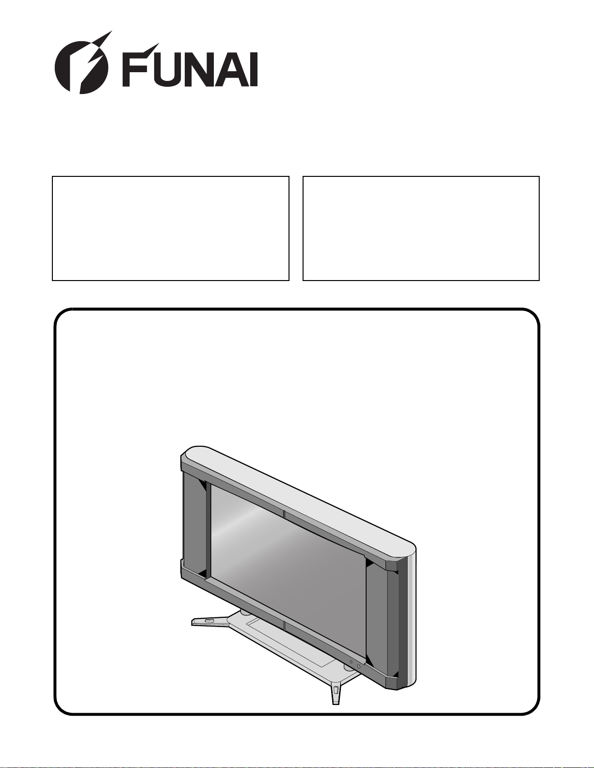
PLASMA DISPLAY
F42PDME
Page 2

IMPORTANT SAFETY NOTICE
Proper service and repair is important to the safe, reliable operation of all
Funai Equipment. The service procedures recommended by Funai and described in this service manual are effective methods of performing service
operations. Some of these service special tools should be used when and
as recommended.
It is important to note that this service manual contains various CAUTIONS
and NOTICES which should be carefully read in order to minimize the risk of
personal injury to service personnel. The possibility exists that improper
service methods may damage the equipment. It also is impo rtant to understand that these CAUTIONS and NOTICES ARE NOT EXHAUSTIVE. Funai
could not possibly know, evaluate and advice the service trade of all conceivable ways in which service might be done or of the possible hazardous
consequences of each way. Consequently, Funai has not undertaken any
such broad evaluation. Accordingly, a servicer who uses a service procedure or tool which is not recommended by Funai must first use all precautions thoroughly so that neither his safety nor the safe operation of the
equipment will be jeopardized by the service method selected.
Page 3

MAIN SECTION
PLASMA DISPLAY
F42PDME
Main Section
I Specifications
I Adjustment Procedures
I Troubleshooting
I Schematic Diagrams
I CBA’s
I Exploded Views
I Parts List
TABLE OF CONTENTS
Specifications............................................................................................... 1-1-1
Important Safety Precautions....................................................................... 1-2-1
Standard Notes for Servicing....................................................................... 1-3-1
Basic Setup and Operating Guide............................................................... 1-4-1
Cabinet Disassembly Instructions................................................................ 1-5-1
Electrical Adjustment Instructions................................................................ 1-6-1
Troubleshooting........................................................................................... 1-7-1
Block Diagrams............................................................................................ 1-8-1
Schematic Diagrams / CBA’s and Test Points............................................. 1-9-1
Waveforms................................................................................................. 1-10-1
Wiring Diagram....................................... ................................. .................. 1-11-1
IC Pin Functions......................................................................................... 1-12-1
Lead Identifications.................................................................................... 1-13-1
Cabinet Exploded Views............................................................................ 1-14-1
Packing Exploded Views............................................................................ 1-14-3
Mechanical Parts List................................................................................. 1-15-1
Electrical Parts List .................................................................................... 1-16-1
Page 4
SPECIFICATIONS
Description Condition
Display Features
Screen Size 920.1 (W) x 518.4 (H) mm, 42 in. Wide VGA panel
Pixel Resolution 852 (H) x 480 (V)
Output Colors 16.7 million
Screen Aspect Ratio 16:9
Contrast Ratio 1000:1
Brightness
Comb Filter Type 3-Dimensional Y/C Separation
Available Input Format 720p/1080i/480p/480i (720p/1080i/480p: Component 2 only)
Sound Output 5W + 5W, 10% THD
Speaker 3 in Round Type x 4
Audio IN 0.5Vrms
470 cd/m
2
(PEAK)
Audio Features
Connectors
Component AV Input (1) SD component video/Y, Cb, Cr, (RCA x 3) - rear
Component AV Input (2) HD component video/Y, Pb, Pr, (RCA x 3) - rear
Composite AV Input (1)
S-Video (1)
Composite AV Input (2)
S-Video (2)
Analog Audio output audio L/R (RCA x 2) - rear
Power In 120V ±10%, 60Hz/AC
Power Consumption 350 W (standby-condition 1.3W)
Operation Temperature 41F - 104F (5°C - 40°C)
Humidity Under 80%
Dimension 1314 (W) x 692 (H) x 149.5 (D) mm
audio L/R (RCA x 2) - rear
Y: 1.0Vp-p (75 Ohm), Cb/Cr: 0.7Vp-p (75 Ohm)
audio L/R (RCA x 2) - rear
Y: 1.0Vp-p (75 Ohm), Pb/Pr: 0.7Vp-p (75 Ohm)
Composite video (RCA x 1) - rear, 1.0Vp-p (75 Ohm)
S-Video (4 pin DIN) - rear
audio L/R (RCA x 2) - rear
Y: 1.0Vp-p (75 Ohm), C: 0.286Vp-p (75 Ohm)
Composite video (RCA x 1) - rear, 1.0Vp-p (75 Ohm)
S-Video (4 pin DIN) - rear
audio L/R (RCA x 2) - rear
Y: 1.0Vp-p (75 Ohm), C: 0.286Vp-p (75 Ohm)
General
1314 (W) x 789 (H) x 393 (D) mm (Incl. Stand)
Weight 112.46 lbs (51 kg)
Note:
Nominal specificati ons represen t the design specificatio ns. All units sh ould be able to approximat e these. Som e
will exceed and so me may drop slightly below thes e specifications. Limit specific ations represent the absolut e
worst condition that still might be considered acceptable. In no case should a unit fail to meet limit specifications.
1-1-1 L0605SP
Page 5
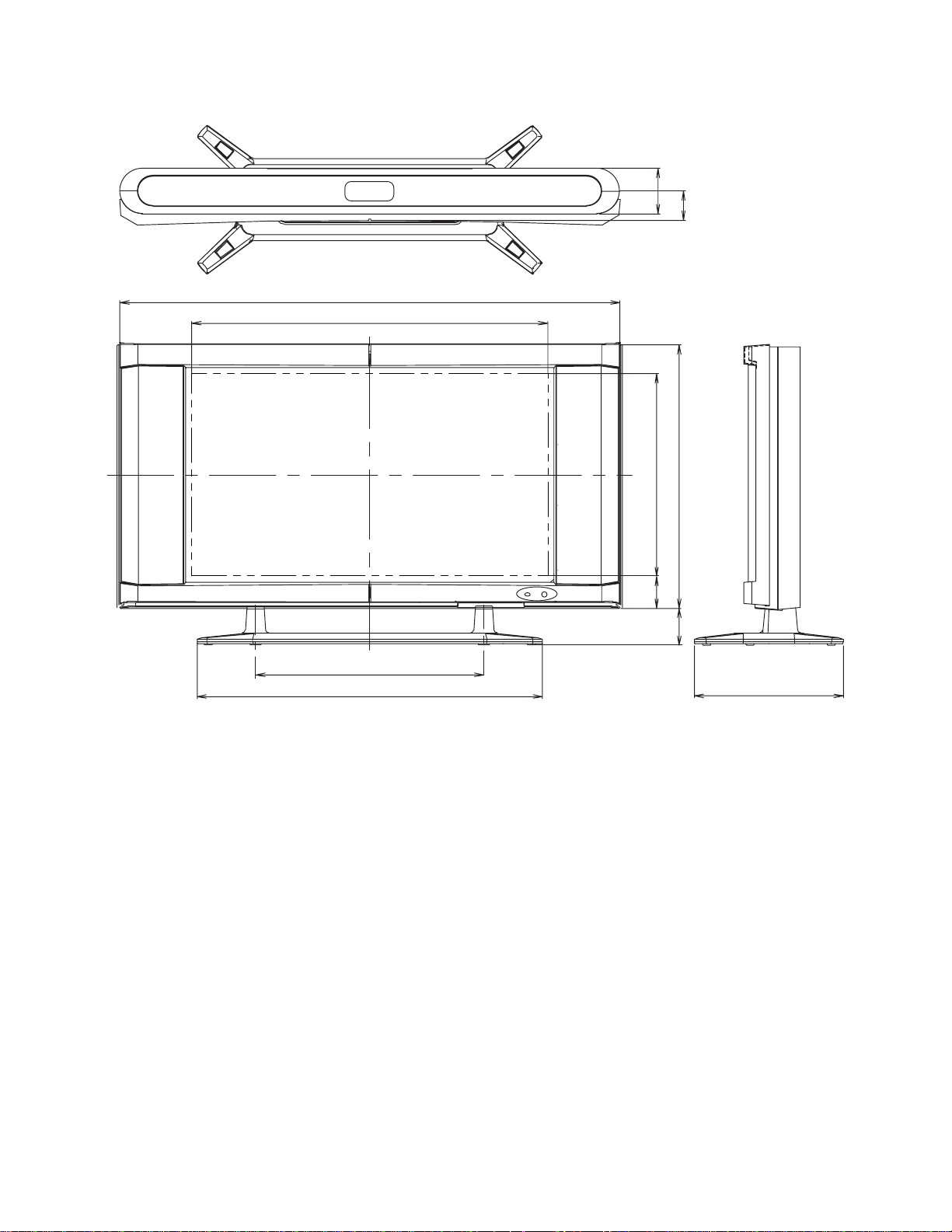
DIMENSIONS
1314
920.1
120
518.483.6
77
692
600
907.47
97
393
1-1-2 L0605SP
Page 6

IMPORTANT SAFETY PRECAUTIONS
Prior to shipment from the fact ory, our products are stri ctly insp ected for recogni zed pr oduct sa fety and elec trical
codes of the countries in which they are to be sold. Howev er, in order to ma intain such c ompliance, it is equally
important to implement the following precautions when a set is being serviced.
Safety Precautions fo r M onitor C ircuit
1. Before returning an instrum ent t o the c ustom -
er, always make a safety check of the entire instru-
ment, including, but not limited to, the following
items:
a. Be sure that no built-in protec tive devic es are de -
fective and have b een defeated during servicing.
(1) Protective shields are provided on this chassis
to protect both the technician an d the customer.
Correctly replace all missing protective shields, including any removed for servicing convenience. (2)
When reinstalling the chassis and/or other assembly in the cabinet, be su re to put back in p lace all
protective devices, including but not limited to,
nonmetallic control knobs, insulating fishpapers,
adjustment and compartment cove rs/shields, and
isolation resistor/capacitor networks. Do not oper-
ate this instrument or permit it to be operated
without all protective devices correctly installed and functioning. Servicers who defeat
safety features or fail to perform safety checks
may be liable for any resulting damage.
b. Be sure that there are no cabinet openings through
which an adult or child might be able to insert their
fingers and contact a hazardous voltage. Such
openings include, but are not limited to, (1) excessively wide cabinet ventilation slots, and (2) an improperly fitted and/or incorrectly secured cabinet
back cover.
c. Leakage Current Cold Check - With the instru-
ment AC plug removed from any AC s ource, con nect an electrical jumper across the two AC plug
prongs. Place the in strument AC swi tch in the on
position. Connect one lead of an oh mmeter to the
AC plug prongs tied together and touch the other
ohmmeter lead in tu rn to each exposed metallic
cabinet part. If the measured resistance is less
than 1.0 megohm or greater than 5.2 megohm, an
abnormality exists that must be corrected before
the instrument is returned to the customer. Repeat
this test with the instrument AC switch in the off position.
d. Leakage Current Hot Check - With the instru-
ment completely reassembled, plug the AC line
cord directly into a 120V AC outlet. (Do not use an
isolation transformer d uring thi s test.) Use a leakage current tester or a metering system that complies with American National Standards Institute
(ANSI) C101.1 Leakage Current for Appliances.
With the instrument AC switc h first in the on posi tion and then in the o ff position, measure from a
known earth ground (metal water pipe, conduit,
etc.) to all exposed metal parts of the instrument
(antennas, handle br ackets, metal cabi net, screw
heads, metallic overlay s, control shafts, etc.), es pecially any exposed metal parts that offer an electrical return path to the chassis. Any current
measured must not exceed 0.75 milli-ampere. Reverse the instrument power cord plug in the outlet
and repeat the test.
ANY MEASUREMENTS NOT WITHIN THE LIMITS
SPECIFIED HEREIN INDICATE A POTENTIAL
SHOCK HAZARD THAT MUST BE ELIMINATED
BEFORE RETURNING THE INSTRUMENT TO
THE CUSTOMER OR BEFORE CONNECTING
THE ANTENNA OR AC CES SORI ES.
2. Read and comply with all caution and safety-related notes on or insid e the cabi net, or on the chassis,
3. Design Alteration Warning - Do not alter or add
to the mechanical or electrical design of th is mon itor. Design alterations and additions, including,
but not limited to circuit mod ifications and the addition of items such as auxiliary audio and/or video
output connections, might a lter the sa fety charac teristics of this receiver and create a hazard to the
user. Any design alterations or additions will void
the manufacturer's warrant y and may make you,
the servicer, responsible for personal injury or
property damage resulting therefrom.
4. Hot Chassis Warning -
a. Some monitor chassi s are electrically connected
directly to one conductor of the AC power cord and
maybe safety-servi ced without an isolati on transformer only if the AC power plug is inserted so that
the chassis is con nec ted to the ground side of the
AC power source . To confirm that the A C power
plug is inserted correctly, with an AC voltmeter,
measure between the chas sis and a known ear th
ground. If a voltage read ing in excess of 1.0V is
obtained, remove and reinsert t he AC power plug
in the opposite polarity and again measure the
voltage potential between the chassis and a
known earth ground.
1-2-1 L0604IMP
Page 7

b. Some monitor chassis normally have 85V
AC(RMS) between chassi s and earth ground regardless of the AC p lug pol arity. This chass is can
be safety-serviced only with an isolation transformer inserted in the p ower lin e betwee n the r ecei ver
and the AC power so urce, for both p erso nnel a nd
test equipment protection.
c. Some monitor chassis have a secondary ground
system in addition to the main chassis ground.
This secondary ground system is not isolated from
the AC power line. The two ground systems are
electrically separated by insulation material that
must not be defeated or altered.
5. Observe orig inal lead dre ss. Take extra ca re to assure correct lead dress in the following areas:a.
near sharp edges,b. near thermally hot parts-be
sure that leads and components do not touch thermally hot parts,c. th e AC supply,d. high voltage,
and,e. antenna wiring. Always inspect in all ar eas
for pinched, out of plac e, or frayed wiring. Ch eck
AC power cord for damage.
6. Components, parts, and/or wiring that appear to
have overheated or are otherwise damaged
should be replaced with components, parts, or wiring that meet origina l specifications. Additionally,
determine the cause of ov erheating and/or damage and, if necessary, take corrective action to remove any potential safety hazard.
7 Product Safety Notice - Some electrical and me-
chanical parts have sp ecial safety -relate d char acteristics which are often not evident from visual
inspection, nor can the protection they give necessarily be obtain ed by replac ing them wi th components rated for higher voltage, wattage, etc.. Parts
that have special safet y characte ristic s are ide ntified by a ( # ) on schematics and in parts lists. Use
of a substitute replacement that does not have the
same safety charac teristics as the recommend ed
replacement part might crea te shock, fire, and/or
other hazards. The product's safety is under review continuously and new instructions are issued
whenever appropriate . Prior to shipme nt from the
factory, our produc ts are strict ly ins pected to con firm they comply with the recognized product safety and electrical code s of the countries in which
they are to be sold. However , in order to maintai n
such compliance, it is equally important to implement the following precautions when a set is being
serviced.
General Caution of Plasma Display
1. Since the Panel module and front filter are made of
glass, sufficient care shall be taken when handling
the broken module and filter in order to avoid injury.
2. If necessary to replace Panel module, this work
must be started after the panel module and the
AC/DC Power supply becomes sufficiently cool.
3. Special care must be taken with the display area to
avoid damaging its surface.
4. The Panel Module sha ll not be touched wit h bare
hands to protect its surface from stains.
5. It is recommended to use clean soft gloves during
the replacing work of the Panel module in order to
protect, not only the display area of the panel module but also the serviceman.
6. The Chip Tube of the panel module (located upper
left of the back of the panel modu le) and flexible
cables connecting Pane l glasses to the drive circuitry Printed Wiring Boards (P.W.B.) are very
weak, so sufficient c are must be taken t o prevent
breaking or cutting any of these. I f the Chip Tube
breaks the panel mo dul e wi ll ne ve r w ork, re pla ce ment for a new plasma panel module will be needed.
7. Signal, power supply P.W.B.’s and PDP driving circuits P.W.B.’s are assembled o n the rear side of
the PDP module, take special care with this fragile
circuitry; particularly, Flexible Printed Circuits
bonded to surrounding edges of the glass panel.
They are not strong enough to withstand harsh
outer mechanical forces. Avoid tou ching th e flexible printed circuits by not only your hands, but also
tools, chassis, or any oth er obj ec t. E xtre me bend ing of the connectors must be avoided too. In case
the flexible printed c ircuits are damage d, the corresponding addres sed portions of the screen will
not be lit and exchange of a glass panel will be required.
1-2-2 L0604IMP
Page 8

PDP Module Handling
Precautions during Servicing
When there is need to rep lace a brok en PDP m odule
which is the displaying device from the Plasma display
unit, consider the following:
1. When carrying the PDP module, two persons
should stand at both shorter-edge sides of the
glass-panel and transport it with their palms. Avoid
touching the Flexible Prin ted Circuits or the chip
tube on the corner of the glass-panel. Handle only
by the surface of the glass panel.
2. When carrying PDP module, watch surrounding
objects, such as tables, and also do not carry it
alone since it may be dangerous and it will be damaged due to excessive stress to the module (glasspanel).
3. Please do not stand the m odule with the edge of
the glass-panel on the table since this might result
in damage to the glass-pa nel and /or flex ible printed circuits due to exces sive stress to the modul e
(glass-panel).
A. Parts identified by th e ( # ) symbol are critical for
safety.
Replace only with part number specified.
B. In addition to safety, other parts and assemblies
are specified for conformance with regulations applying to spurious radiati on. These must also be
replaced only with specified replacements.
Examples: RF converters, RF cables, noise blocking capacitors, and noise blocking filters, etc.
C. Use specified internal wiring. Note especially:
1) Wires covered with PVC tubing
2) Double insulated wires
3) High voltage leads
D. Use specified insulating materials for hazardous
live parts. Note especiall y:
1) Insulation Tape
2) PVC tubing
3) Spacers
4) Insulators for transistors.
E. When replacing AC primary side components
(transformers, power cord, etc.), wrap ends of
wires securely about the terminals before solder ing.
F. Observe that the wires do not contact heat produc-
ing parts (heatsinks, oxide metal film resistors, fusible resistors, etc.)
G. Check that replaced wires do not contact sharp
edged or pointed parts.
H. Also check areas surrounding repaired locations.
I. Use care that foreign objects (screws, solder drop-
lets, etc.) do not remain inside the set.
J. When connecting or disconnecting the internal
connectors, first, discon nect the AC plug from the
AC supply outlet.
1-2-3 L0604IMP
Page 9
Safety Check after Servicing
Examine the area surrounding the repaired location
for damage or deterioration. Observe that screws,
parts and wires have been returned to original positions. Afterwards, perform th e fol lo wing tes ts and c on firm the specified values in orde r to verify comp liance
with safety standards.
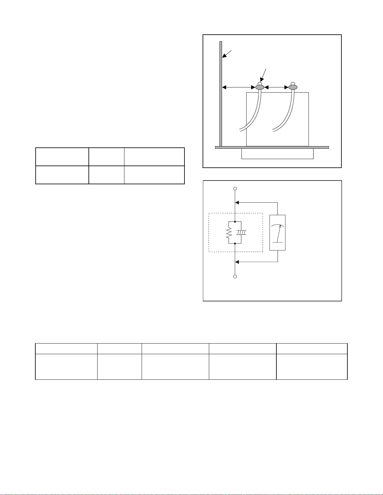
1. Clearance Distance
When replacing primary circuit components, confirm
specified clearance d istance (d) a nd (d') betwee n soldered terminals, and between terminals and surrounding metallic parts. (See Fig. 1)
T able 1 : Ratings for selected area
AC Line Voltage Region
110 to 130 V
Note: This table is unofficial and for reference only. Be
sure to confirm the precise values.
USA or
CANADA
Clearance
Distance (d) (d')
≥ 3.2 mm
(0.126 inches)
2. Leakage Current Test
Confirm the specified (or lower) leakage current between B (any two parts or contacts, between any part
or contact and either pole of the power cord plug
prongs) and ext ernally exposed access ible parts (RF
terminals, antenna terminals, video and audio input
and output terminals, microphone jacks, earphone
jacks, etc.) is lower than or equal to the spec ified value in the table below.
Measuring Method: (Power ON)
Insert load Z between B (any two parts or contacts,
between any part or contact and either pole of the
power cord plug prongs) and exposed accessible
parts. Use an AC voltmeter to measure across both
terminals of load Z. See Fig. 2 and following table.
Z
1.5kΩ
Chassis or Secondary Conductor
Primary Circuit Terminals
dd'
Exposed Accessible Metal Part
AC Voltmeter
0.15µF
One of Power Cord
B
Plug Prongs
(High Impedance)
Fig. 1
Fig. 2
Table 2: Leakage current ratings for selected areas
AC Line Voltage Region Load Z Leakage Current (i) Earth Ground (B) to:
0.15µF CAP. & 1.5kΩ
110 to 130 V USA
Note: This table is unofficial and for reference only. Be sure to confirm the precise values.
RES. connected in
parallel
1-2-4 L0604IMP
i≤0.75mA peaks
Exposed accessible
parts
Page 10
STANDARD NOTES FOR SERVICING
Circuit Board Indications
a. The output pin of the 3 pin Regulator ICs is indicat-
ed as shown.
Top Vie w
Out
b. For other ICs, pin 1 a nd ever y fifth pin are in dic at -
ed as shown.
Pin 1
c. The 1st pin of every male connector is indicated as
shown.
Pin 1
Input
In
Bottom View
5
10
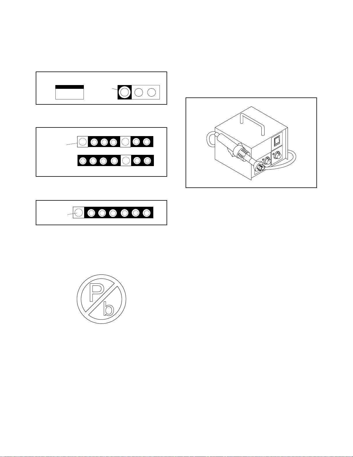
Pb (Lead) Free Solder
Pb free mark will be found on PCBs which use Pb
free solder. (Refer to figure.) For PCBs with Pb
free mark, be sure to use Pb free solder. For PCBs
without Pb free mark, use standard solder.
Pb free mark
How to Remove / Install Flat Pack-IC
1. Removal
With Hot-Air Flat Pack-IC Desoldering Machine:
(1) Prepare the hot-air flat pack-IC desoldering ma-
chine, then apply hot air to the Flat Pack-IC (about
5 to 6 seconds). (Fig. S-1-1)
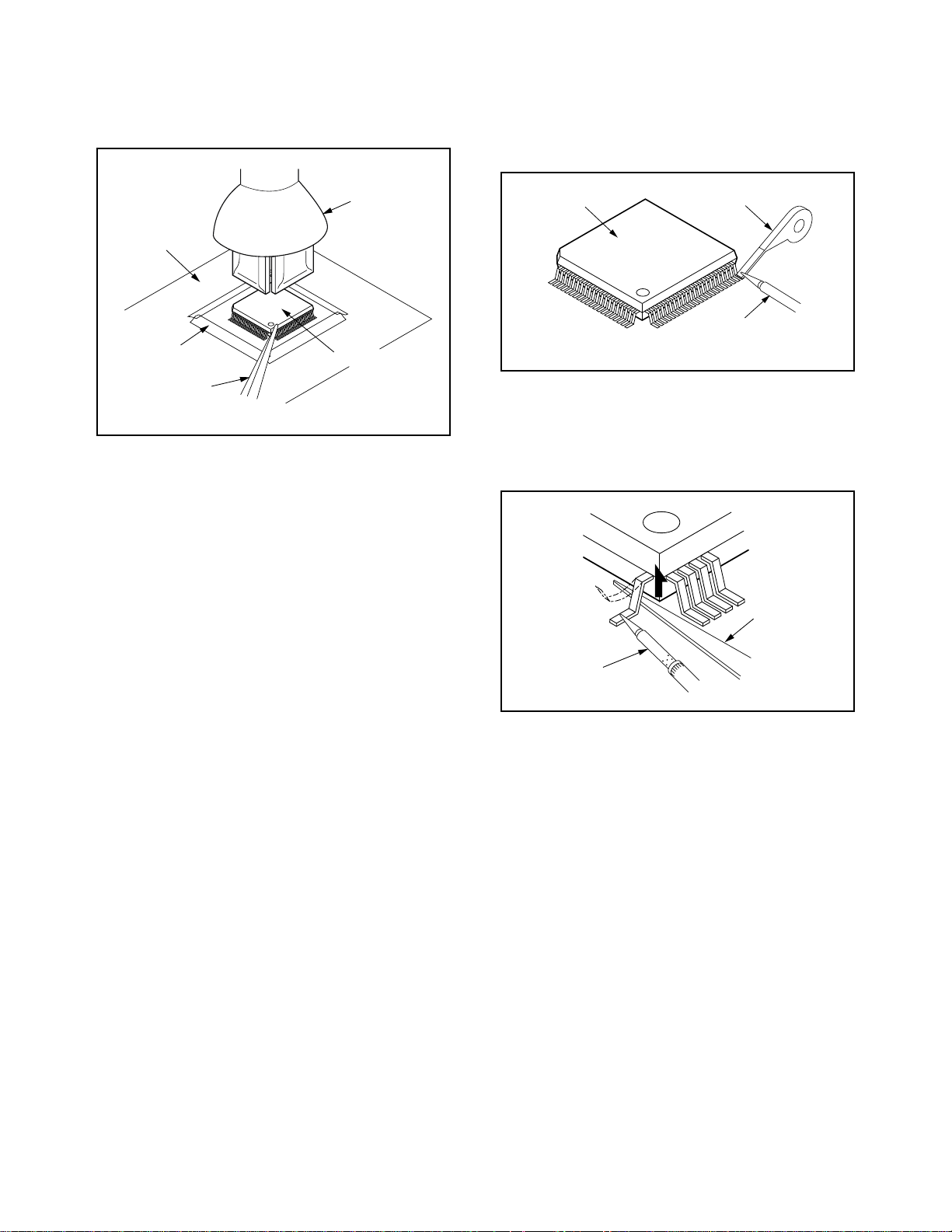
Fig. S-1-1
(2) Rem ove the flat pack-IC with tweezers while ap-
plying the hot air.
(3) B ottom of the flat pack-I C is fixed wi th glue to the
CBA; when removing entire flat pack-IC, first apply
soldering iron to center of the flat pack-IC and heat
up. Then remove (glue will be melted). (Fig. S-1-6)
(4) Release the flat pack-IC from the CBA using twee-
zers. (Fig. S-1-6)
Caution:
1. The Flat Pack-IC shape may differ by models. Use
an appropriate hot-air flat pack-IC desoldering ma-
chine, whose shape matches that of the Flat Pack-
IC.
2. Do not supply hot air to the chip parts around the
flat pack-IC for over 6 seconds because damage
to the chip parts may occur. Put masking tape
around the flat pack-IC to protec t other par ts from
damage. (F ig. S-1-2)
1-3-1 L14STA2
Page 11
3. The flat pack-IC on the CBA is affixed with glue, so
be careful not to bre ak or d ama ge the f oil of each
pin or the solder l ands under the IC when remov ing it.
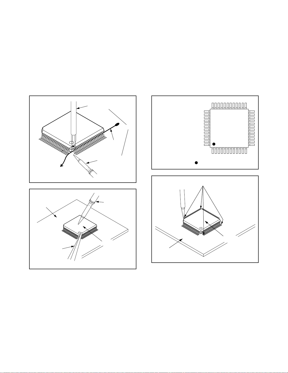
With Soldering Iron:
(1) Us ing desoldering braid, remove the solder from
all pins of the flat pack-IC. When you use solder
flux which is applie d to al l pins o f th e flat pac k-IC,
you can remove it easily. (Fig. S-1-3)
CBA
Masking
Tape
Tweezers
Hot-air
Flat Pack-IC
Desoldering
Machine
Flat Pack-IC
Fig. S-1-2
Flat Pack-IC
Desoldering Braid
Soldering Iron
Fig. S-1-3
(2) Li ft each lead of the flat pack-IC upward one by
one, using a sharp pin or wi re to which solder will
not adhere (iron wire). When heating the pins, use
a fine tip soldering iron or a hot air desoldering machine.(Fig. S-1-4)
Sharp
Pin
Fine Tip
Soldering Iron
(3) B ottom of the flat pack-I C is fixed wi th glue to the
CBA; when removing entire flat pack-IC, first apply
soldering iron to center of the flat pack-IC and heat
up. Then remove (glue will be melted). (Fig. S-1-6)
(4) Release the flat pack-IC from the CBA using twee-
zers. (Fig. S-1-6)
With Iron Wire:
(1) Us ing desoldering braid, remove the solder from
all pins of the flat pack-IC. When you use solder
flux which is applie d to al l pins o f th e flat pac k-IC,
you can remove it easily. (Fig. S-1-3)
(2) Affix the wire to a workbench or solid mounting
point, as shown in Fig. S-1-5.
(3) While heating the pins using a fine tip soldering
iron or hot air blower, pull up the wire as the solder
melts so as to lift the IC leads fr om the CBA contact pads as shown in Fig. S-1-5.
Fig. S-1-4
1-3-2 L14STA2
Page 12
(4) Bottom of the flat pack -IC is fixe d with glue to the
CBA; when removing entire flat pack-IC, first apply
soldering iron to center of the flat pack-IC and heat
up. Then remove (glue will be melted). (Fig. S-1-6)
(5) Release the flat pack-IC from the CBA using twee-
zers. (Fig. S-1-6)
Note:
When using a soldering iron, care must be taken to
ensure that the flat pack-IC is not being held by
glue. When the flat pack-IC i s removed from the
CBA, handle it gently because it may be damaged
if force is applied.
2. Installation
(1) Us ing desoldering braid, remove the solder from
the foil of each pin of the fla t pack-IC o n the CBA
so you can install a replacement flat pack-IC more
easily.
(2) T he "I" mark on the flat pac k-IC indicates pin 1.
(See Fig. S-1-7.) Be sure this mark matches the 1
on the PCB when positioning for installation. Then
pre- solder the four corners of the flat pack-IC.
(See Fig. S-1-8.)
(3) Solder all pins of the flat pack-IC. Be sure that
none of the pins have solder bridges.
To Solid
Mounting Point
CBA
Tweezers
Hot Air Blower
Iron Wire
Soldering Iron
Fig. S-1-5
Fine Tip
Soldering Iron
Flat Pack-IC
or
Example :
Pin 1 of the Flat Pack-IC
is indicated by a " " mark.
Presolder
CBA
Fig. S-1-7
Flat Pack-IC
Fig. S-1-6
Fig. S-1-8
1-3-3 L14STA2
Page 13
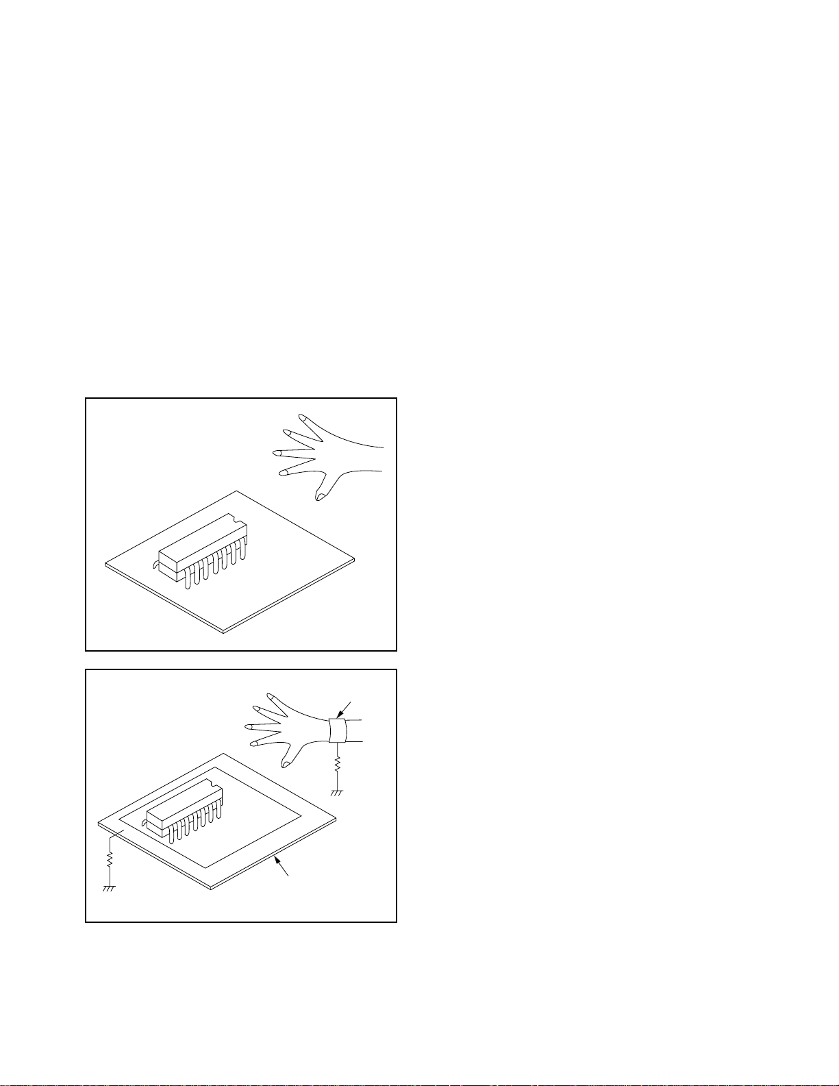
Instructions for Handling
Semiconductors
Electrostatic breakdown of the semiconductors may
occur due to a poten tial differen ce caused b y electrostatic charge during unpacking or repair work.
1. Ground for Human Body
Be sure to wear a grounding band (1M Ω) that is prop erly grounded to remove any static electricity that may
be charged on the body.
2. Ground for Workbench
Be sure to place a conductive sheet or copper plate
with proper grounding (1MΩ) on the workbench or
other surface, where the semiconductors are to be
placed. Becaus e the static elec tricity cha rge on cloth ing will not esc ape throug h the body grounding ban d,
be careful to avoid contacting semiconductors with
your clothing.
<Incorrect>
<Correct>
1MΩ
CBA
Grounding Band
1MΩ
CBA
Conductive Sheet or
Copper Plate
1-3-4 L14STA2
Page 14
1
2
3
4
5
6
7
r
r
-
M
3
3
S-VIDEO
VIDEO
L
R
S-VIDEOVIDEO
LR
L
R
VIDEO1
S-VIDEO1
VIDEO2
S-VIDEO2
AUDIO
AUDIO OUT
AC IN
AUDIO
Pr
L
Y
Pb
R
Cr
L
Y
Cb
R
COMPONENT1
COMPONENT2
Input Terminals
6 7 8 9
INPUT SELECTVOLUME
POWER
AC IN
S-VIDEO
VIDEO
L
R
L
R
AUDIO
AUDIO OUT
AUDIO
Pr
L
Y
Pb
R
Cr
L
Y
Cb
R
COMPONENT1
COMPONENT2
VIDEO1
S-VIDEO1
VIDEO2
S-VIDEO2
S-VIDEOVIDEO
LR
2
1
4
Infrared Sensor
5
INPUT SELECTVOLUME
POWER
INPUT SELECTVOLUME
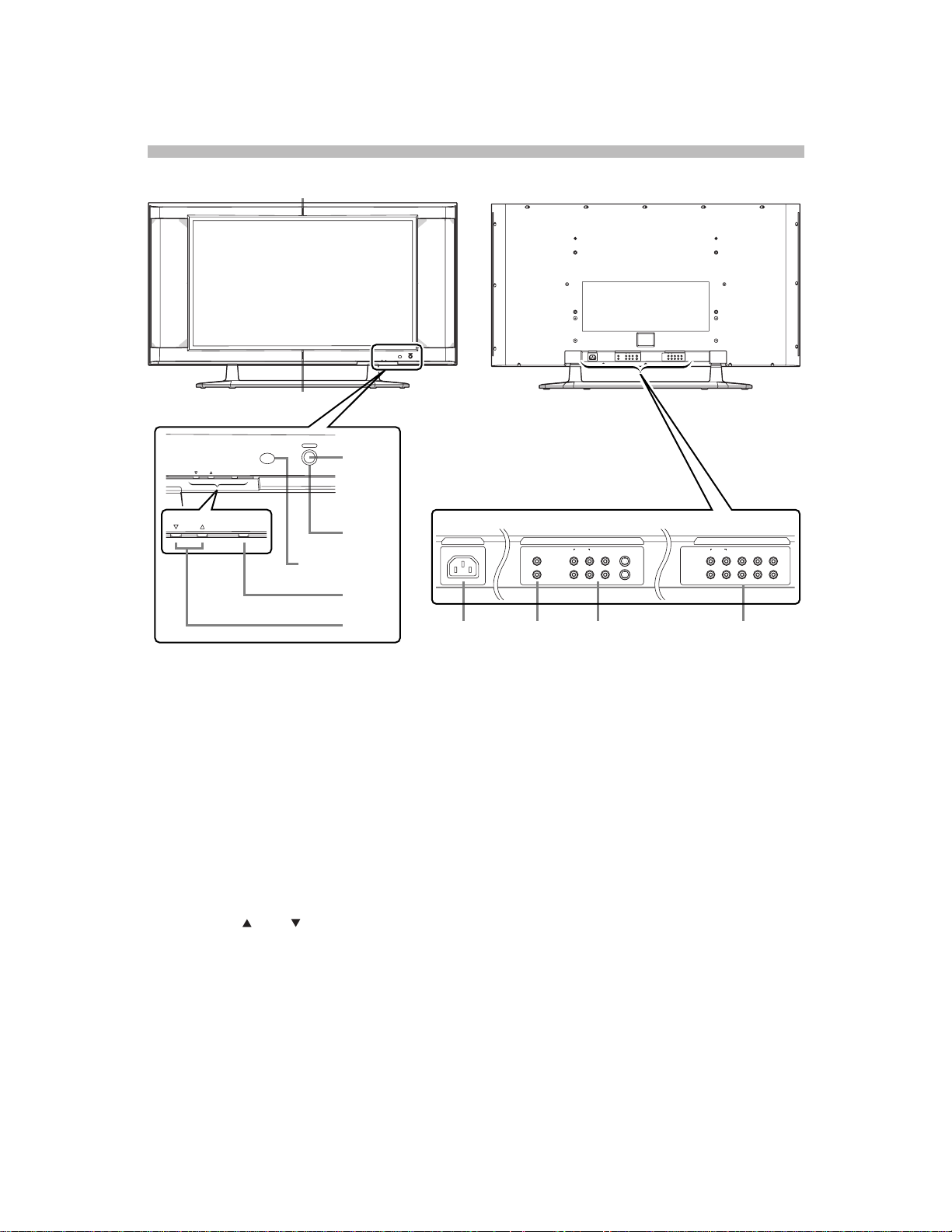
BASIC SETUP AND OPERATING GUIDE
AIN UNIT
Front Rear
POWER button: Turns the power ON or in
STANDBY.
POWER indicator: Lights up (Blue) when
the power is in the standby mode. Lights up
(Green) when the power is ON.
STANDBY indicator: Lights up when the
power is in the standby mode. Disappears
when the power is ON.
8
AUDIO/VIDEO/S-VIDEO: Input terminals fo
an audio and video signal. You can select
either VIDEO or S-VIDEO.
9
COMPONENT: Input terminals for a compo
nent signal. You can make a Y-Cb-Cr interlaced connection to component 1 or Y-Pb-P
progressive or interlaced connection to com
ponent 2.
INPUT SELECT button: Selects input terminals.
VOLUME (up) / (down) button:
Increases or decreases the volume.
AC IN terminal: Connect the supplied
power cable for a standard AC outlet.
AUDIO OUT: Output terminals for audio.
1-4-1 L0605IB
Page 15
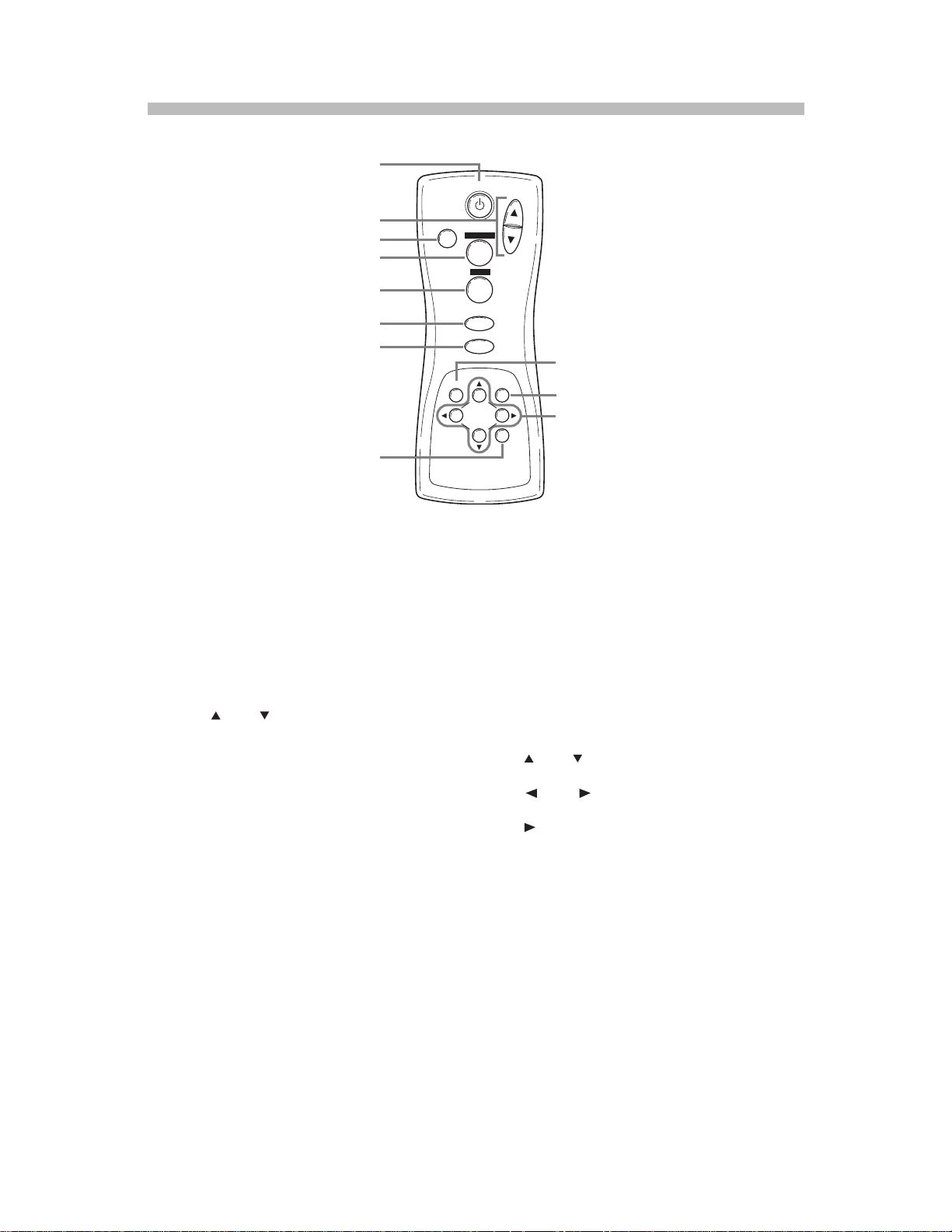
R
1
2
3
4
5
6
7
8
POWER
INPUT SELECT
DISPLAY
MENU
PREVIOUS
SLEEP
VOL
MUTE
SCREEN MODE
STILL
1
2
3
4
5
6
7
8
9
10
11
EMOTE CONTROL
POWER button: Turns the main power ON
or in STANDBY.
VOL (up) / (down) button: Increases or
decreases the volume.
MUTE button: Turns the audio off or on.
SCREEN MODE button: Selects aspect
ratios available for the screen.
STILL button: Pauses the image shown on
the screen.
INPUT SELECT button: Selects input termi-
nals.
DISPLAY button: Displays the name of the
selected input terminal on the screen.
SLEEP button: Sets the sleep timer.
9 MENU button: Accesses the setup menu,
allowing you to access various settings.
10
PREVIOUS button: Moves up one level in
the setup menu.
11
(up) / (down) button: Selects the vari-
ous modes in the setup menu.
(left) / (right) button: Selects and
adjusts levels for the various settings.
(enter) button: Also used as the enter
button.
1-4-2 L0605IB
Page 16
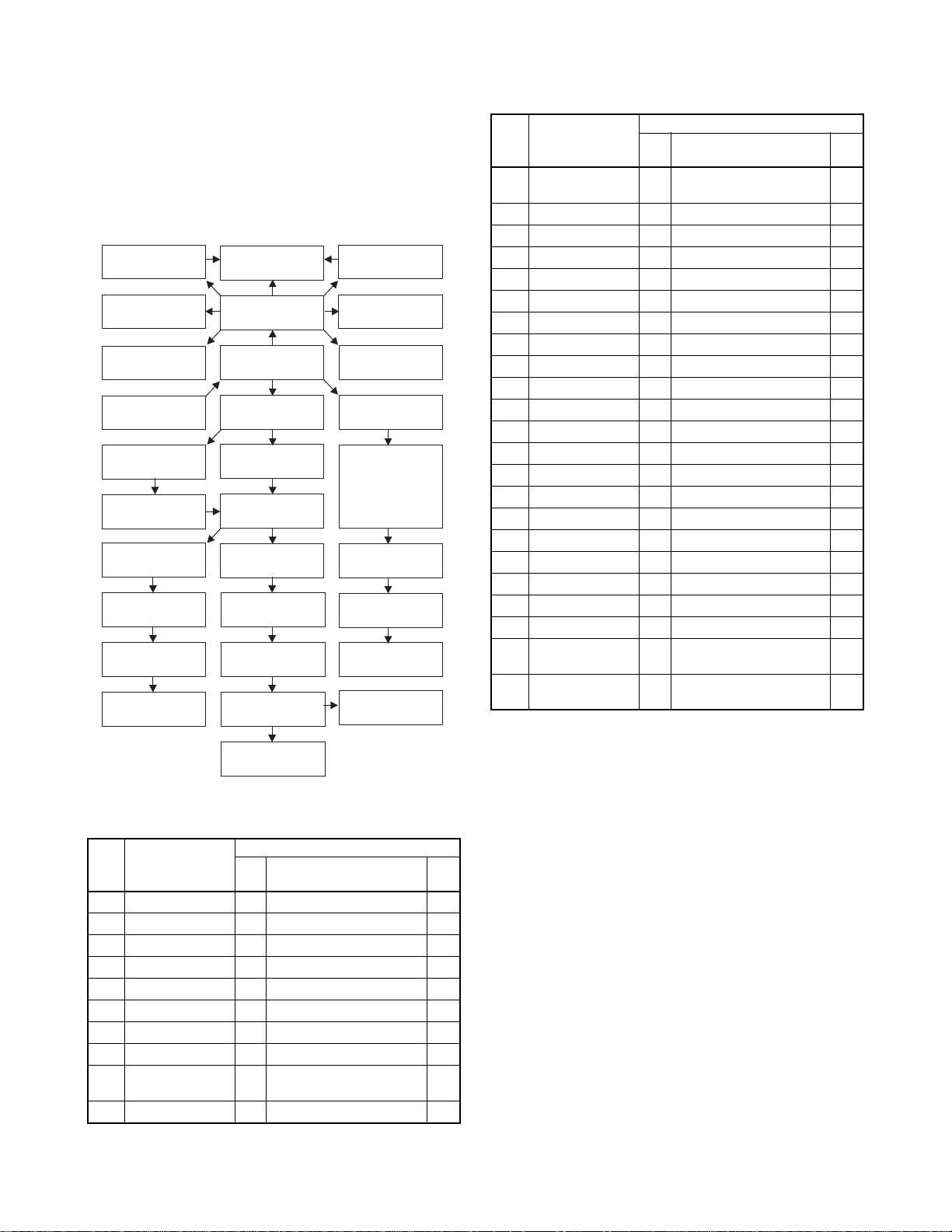
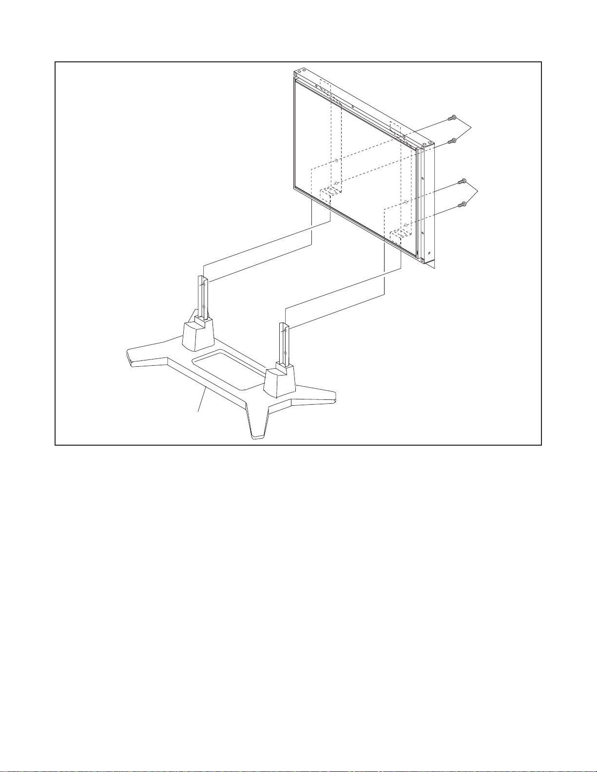
CABINET DISASSEMBLY INSTRUCTIONS
e
r
1. Disassembly Flowchart
This flowchart indicate s the disassem bly steps for the
cabinet parts, and the CBA in order to g ain access to
item(s) to be servic ed. Wh en rea ssemb ling, fol low th e
steps in reverse order. Bend, route and dress the
cables as they were.
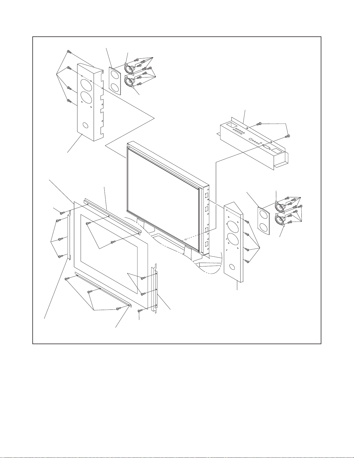
[22] Filter
Holder(L)(s)
[11] LED A CBA
and LED B CBA
[13] Decoration
Panel
[1] Back Cabinet
[6] Analog CBA
[7] Filter CBA
[25] Stand Unit
[26] Stand
Cover
[27] Stand(s)
[28] Stand Base
[24] Optical
Filter
[9] Front Cabinet
Assembly
[2] Rear Cabinet
[3] PCB Shield
Plate
[5] Digital CBA
[8] PCB Holder
[21] Jack Cover
[29] Chassis
Bracket(s)
[30] Panel
Spacer(s)
[31] SP Holder
Plate(s)
[32] Plasma
Display Module
2. Disassembly Method
Step/
Loc.
No.
1 Back Cabinet 1 17(S-1), 5(S-2) 1
2 Rear Cabinet 2 22(S-3) 2
3 PCB Shield Plate 3 12(S-4), CLN8 3
4 Speaker Cover(s) 3 14(S-5) 4
5 Digital CBA 4 4(S-6), 3(S-7) 5
6 Analog CBA 4 4(S-8), 4(S-9) 6
7 Filter CBA 4 2(S-10), Two connectors 7
8 PCB Holder 4 4(S-11) 8
9
10 Brand Plate 5 2(S-13) 10
Part
Front Cabinet
Assembly
Fig. NoRemove/*unlock/release/
unplug/unclamp/desolder
5 14(S-12) 9
[23] Filter
Holder(S)(s)
[12] Switch CBA
[10] Brand Plat
[4] Speaker
Cover(s)
[14] Speaker-1
[15] Speaker-2
[16] Speaker-3
[17] Speaker-4
[18] Speaker
Spacer(s)
[19] Speaker
Holder(L)
[20] Speaker
Holder(R)
[33] Panel Holde
Assembly
Removal
Note
Step/
Loc.
No.
11
12 Switch CBA 5 3(S-14) 11
13 Decoration Panel 6 20(S-15), 2(S-16) 12
14 Speaker-1 7 2(S-17) 13
15 Speaker-2 7 2(S-18) 14
16 Speaker-3 7 2(S-19) 15
17 Speaker-4 7 2(S-20) 16
18 Speaker Spacer(s) 7 ---------- 19 Speaker Holder(L) 7 4(S-21) 17
20 Speaker Holder(R) 7 4(S-22) 18
21 Jack Cover 7 2(S-23) 19
22 Filter Holder(L)(s) 7 6(S-24) 20
23 Filter Holder(S)(s) 7 6(S-25) 21
24 Optical Filter 7 ---------- 25 Stand Unit 8 4(S-26) 22
26 Stand Cover 9 8(S-27), 10(S-28) 23
27 Stand(s) 9 4(S-29), 6(S-30) 24
28 Stand Base 9 ---------- 29 Chassis Bracket(s) 10 8(S-31), 8(S-32) 25
30 Panel Spacer(s) 10 8(S-33) 26
31 SP Holder Plate(s) 10 4(S-34) 27
32
33
Part
LED A CBA and
LED B CBA
Plasma Display
Module
Panel Holder
Assembly
Fig. NoRemove/*unlock/release/
unplug/unclamp/desolder
5 ---------- -
10 12(S-35) 28
10 ---------- -
Removal
Note
↓↓ ↓ ↓ ↓
(1) (2) (3) (4) (5)
Note:
(1) O rder of steps i n procedu re. When reass embling,
follow the steps i n reverse or der. These n umbers
are also used as the Identification (location) No. of
parts in figures.
(2) Parts to be removed or installed.
(3) Fig. No. showing procedure of part location
(4) Identification of part to be removed, unhooked, un-
locked, released, unplugged, unclamped, o r des-
oldered.
S=Screw, P=Spring, L=Locking Tab, CN=Con-
nector, *=Unhook, Unlock, Release, Unplug, or
Desolder
2(S-2) = two Screws (S-2)
(5) Refer to the following "Reference Notes in the
Table.
1-5-1 L0605DC
Page 17

Reference Notes in the Table
Caution:
Refer to "General Caution of Plasma Display" and
"PDP Module Handling" of "IMPORTANT SAFETY
PRECAUTIONS" section not to injure and/or break the
Plasma Display Module.
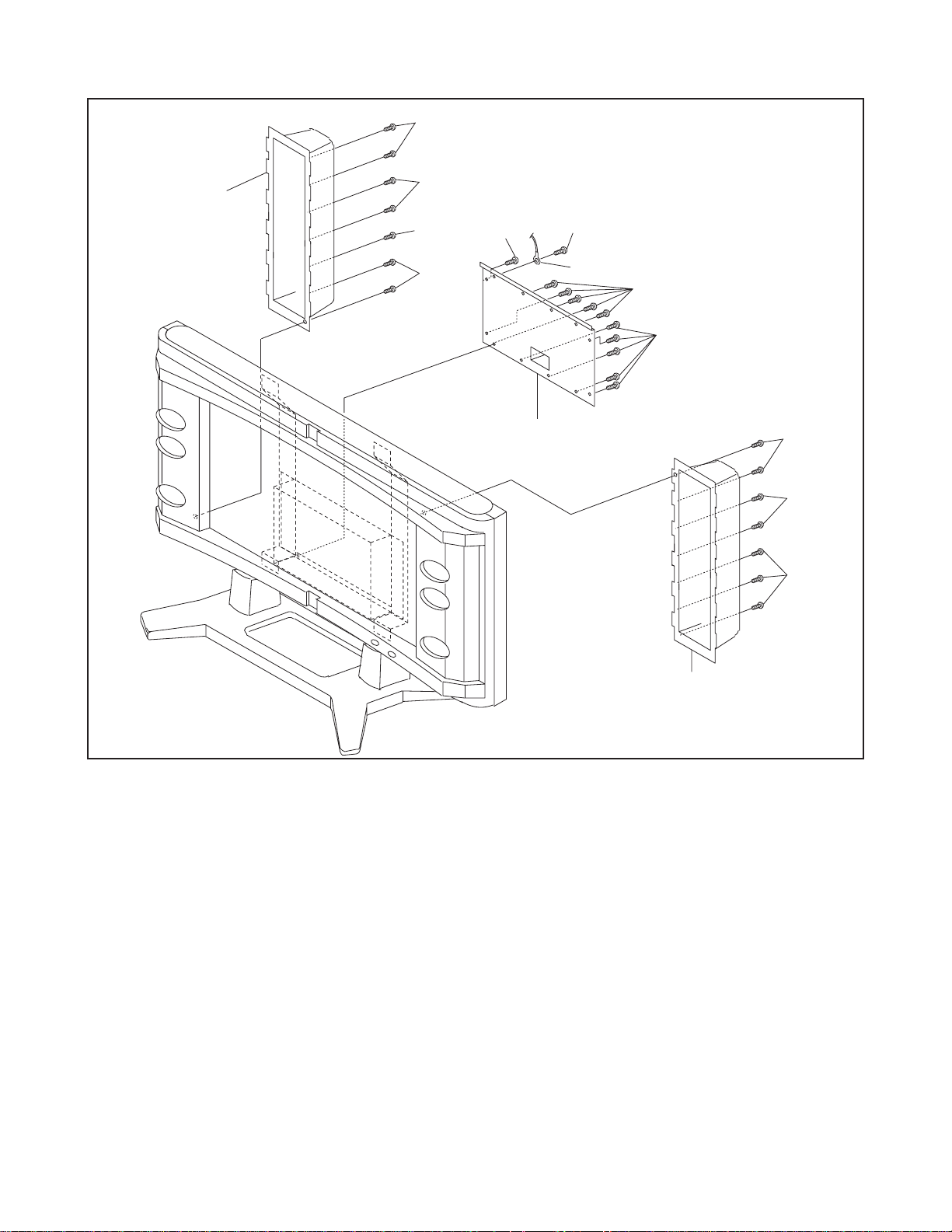
1. Removal of the Back Cabinet. Remove screws
17(S-1) and 5(S-2).
2. Removal of the Rear Cabinet. Remove screws
22(S-3).
3. Removal of the P CB Shiel d Plate . Remo ve screw s
12(S-4) and wire assembly CLN8.
4. Removal of the Speaker Cover(s). Remove screws
14(S-5).
5. Removal of the Digital CBA. Disconnect connectors *CN1701, *CN1702, *CN1 703, *CN1704, and
*CN1709, and remove screws 4(S-6) and 3(S-7).
6. Removal of the An alog CBA. Disconnect connectors *CN201, *CN203, *CN204, *C N501, *CN502,
*CN701, *CN801, and *CN802, and remove
screws 4(S-8) and 4(S-9).
7. Removal of the Filter CBA. Disconnect connecto r
*CN801, and remove two connectors, then remove
screws 2(S-10).
8. Removal of the PCB Ho lder. Remove screws 4(S-
11).
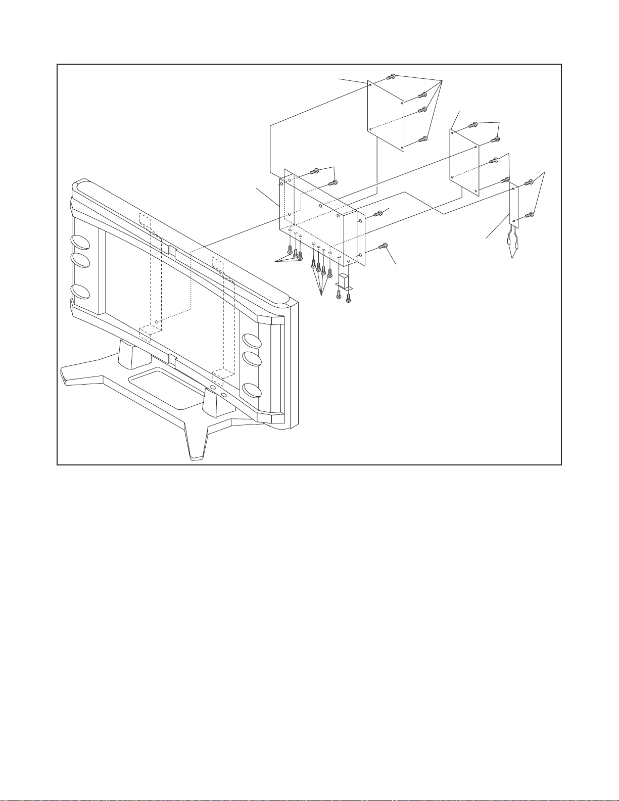
9. Removal of the Front Cabinet Assembly. Remove
screws 14(S-12).
10.Removal of th e Brand Plate. Remov e screws 2(S-
13).
11. Re moval of the Switch CBA. Re move screws 3(S-
14) and disconnect connector *CN751.
12.Removal of th e Decorati on Pane l. Remov e screws
20(S-15) and 2(S-16).
13.Removal of the Speaker-1. Remove screws 8(S-
17).
14.Removal of the Speaker-2. Remove screws 8(S-
18).
15.Removal of the Speaker-3. Remove screws 8(S-
19).
16.Removal of the Speaker-4. Remove screws 8(S-
20).
17.Removal of the Speaker Holder(L). Remove
screws 4(S-21).
18.Removal of the Speaker Holder(R). Remove
screws 4(S-22).
19.Remov al of the Jack Cove r. Remove scre ws 2(S-
23).
20.Removal of the Filter Holder(L)(s). Remove screws
6(S-24).
21.Removal of the Filter Holder(S)(s). Remove screws
6(S-25).
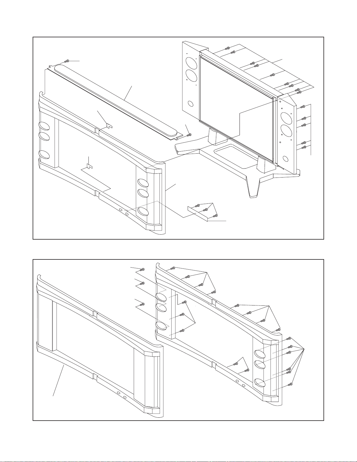
22.Removal of the Stand Unit. Remove screws 4(S-
26).
23.Removal o f the Stand Cover. Remove screws 8(S-
27) and 10(S-28).
24.Removal of the Stand(s). Remove screw s 4(S-29)
and 6(S-30).
25.Removal of the Chassis Bracket. Remove screws
8(S-31) and 8(S-32).
26.Removal of the Panel Spacer(s). Remove screws
8(S-33).
27.Removal of the SP Holder Plate(s). Remove
screws 8(S-34).
28.Removal of the Plasma Display Module. Remove
screws 12(S-35).
1-5-2 L0605DC
Page 18
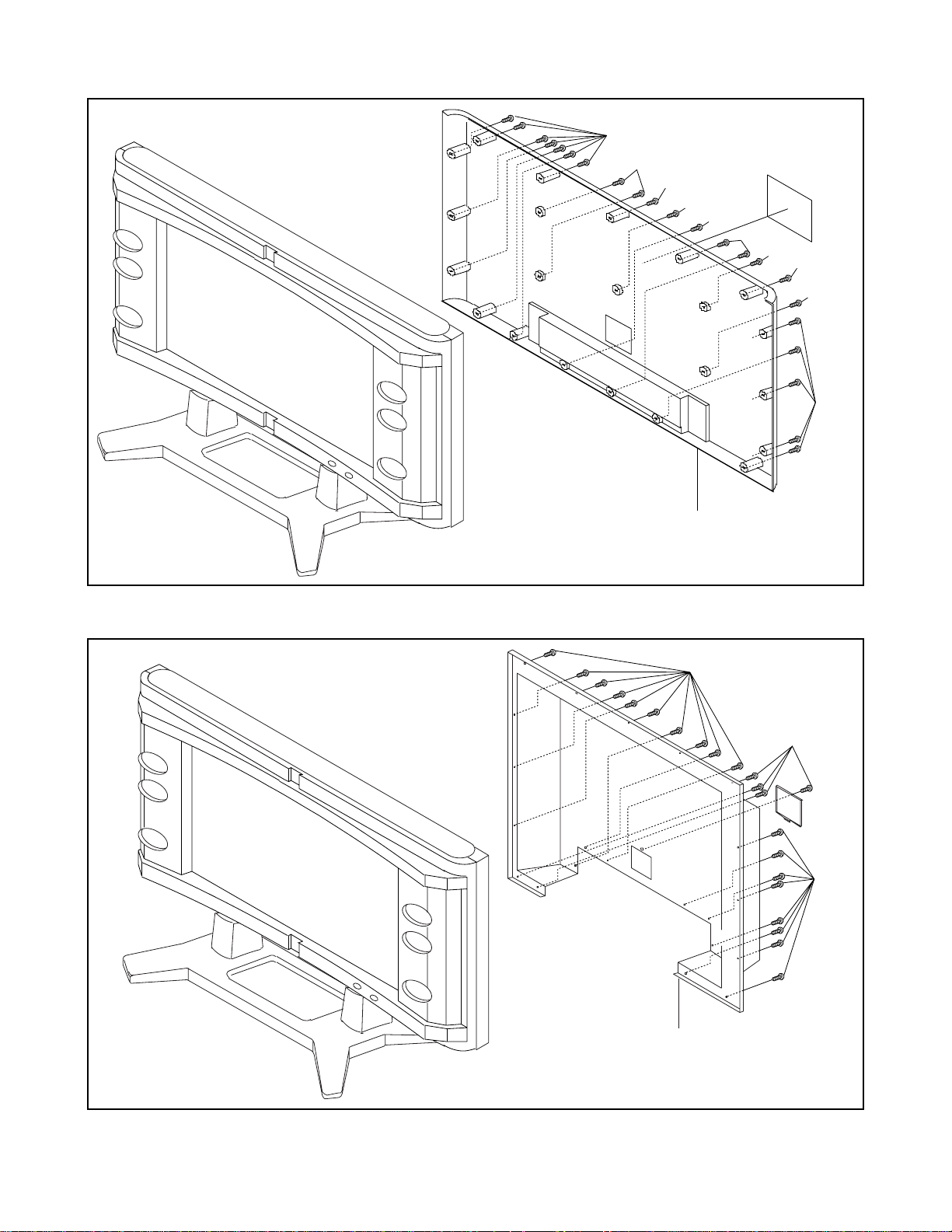
(S-1)
(S-2)
(S-1)
(S-2)
(S-1)
(S-1)
(S-2)
(S-1)
(S-2)
(S-1)
[1] Back Cabinet
Fig. 1
(S-3)
(S-3)
[2] Rear Cabinet
(S-3)
Fig. 2
1-5-3 L0605DC
Page 19
(S-5)
[4] Speaker
Cover
(S-5)
(S-5)
(S-5)
(S-4)
(S-4)
CLN8
[3] PCB Shield Plate
(S-4)
(S-4)
(S-5)
(S-5)
(S-5)
[4] Speaker Cover
Fig. 3
1-5-4 L0605DC
Page 20
[8] PCB Holder
)
[5] Digital CBA
(S-11)
(S-6)
[6] Analog CBA
(S-8)
(S-8)
(S-10
(S-11)
[7] Filter CBA
(S-7)
(S-9)
(S-11)
Connectors
(to AC Inlet)
Fig. 4
1-5-5 L0605DC
Page 21
(S-13)
)
[11] LED
A CBA
[11] LED B CBA
(S-12)
[10] Brand Plate
(S-13)
(S-12)
[9] Front Cabinet
Assembly
(S-14)
[12] Switch CBA
[13] Decoration Panel
(S-15)
(S-15)
(S-15)
Fig. 5
(S-15)
(S-15)
(S-15)
(S-15
(S-16)
Fig. 6
1-5-6 L0605DC
Page 22
[18] Speaker Spacer
[14] Speaker-1
(S-17)
(S-21)
[19] Speaker Holder(L)
[24] Optical Filter
[22] Filter Holder(L)
(S-24)
(S-25)
(S-24)
(S-18)
[15] Speaker-2
[21] Jack Cover
[18] Speaker
Spacer
(S-22)
(S-23)
[16] Speaker-3
(S-19)
(S-20)
[17] Speaker-4
(S-24)
[23] Filter Holder(R)
(S-25)
[20] Speaker Holder(R)
[23] Filter Holder(R)
(S-25)
[22] Filter Holder(L)
Fig. 7
1-5-7 L0605DC
Page 23
(S-26)
(S-26)
[25] Stand Unit
Fig. 8
1-5-8 L0605DC
Page 24
[26] Stand Cover
[28] Stand Base
[27] Stand
(S-27)
(S-29)
(S-30)
(S-29)
(S-30)
(S-27)
(S-29)
[27] Stand
(S-29)
(S-30)
(S-30)
(S-27)
(S-28)
(S-28)
(S-27)
(S-28)
(S-27)
Fig. 9
1-5-9 L0605DC
Page 25
[31] SP Holder Plate
r
[32] Plasma Display
Module
[30] Panel Spacer
(S-33)
[29] Chassis Bracket
(S-31)
(S-32)
[30] Panel Space
(S-31)
(S-35)
(S-34)
(S-35)
(S-34)
(S-35)
(S-35)
[33] Panel Holder
Assembly
(S-35)
(S-35)
(S-35)
(S-35)
(S-34)
(S-34)
(S-33)
[30] Panel Spacer
[31] SP Holder Plate
(S-33)
(S-32)
(S-31)
(S-33)
(S-32)
(S-32)
(S-31)
[29] Chassis Bracket
Fig. 10
1-5-10 L0605DC
Page 26
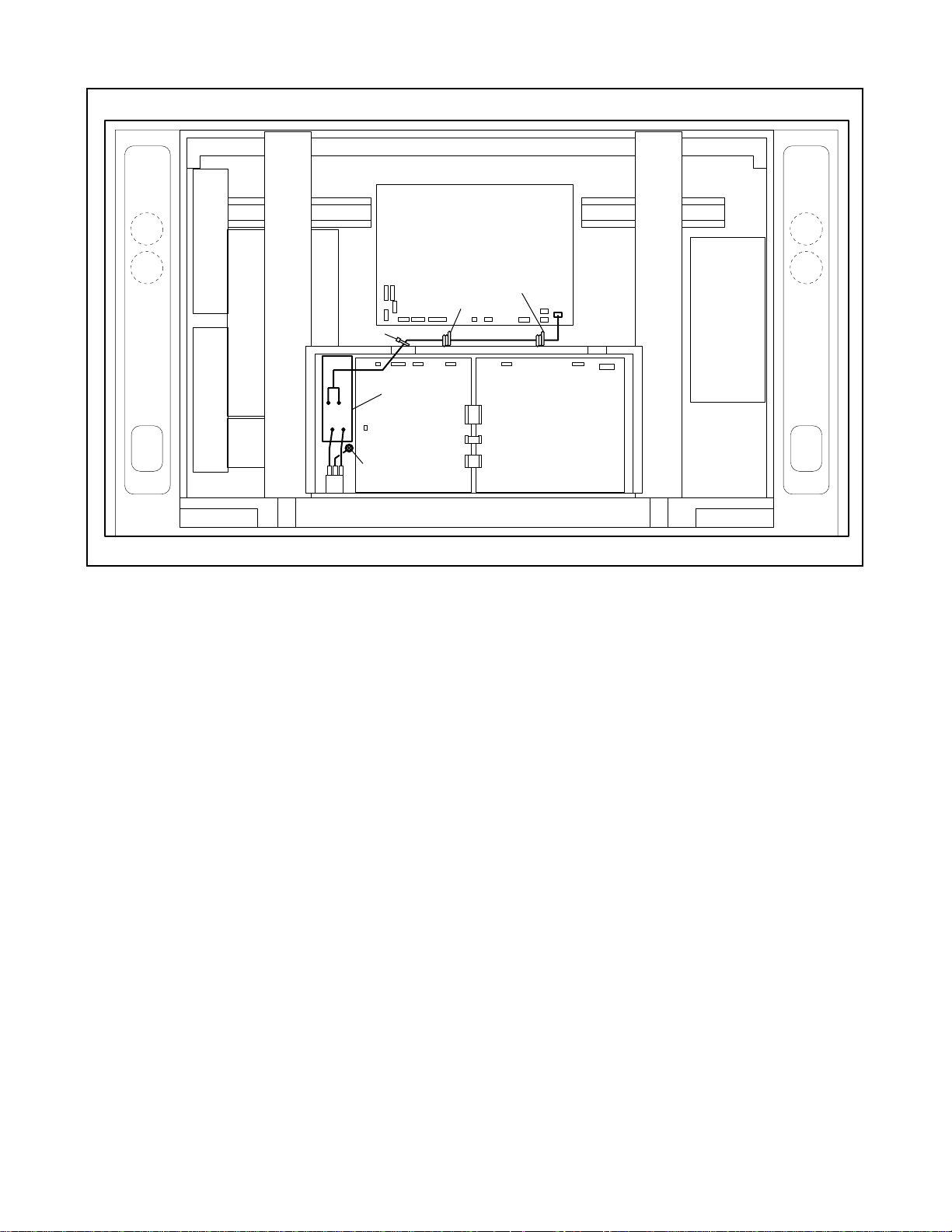
Plasma Display Cable Wiring Diagram
Cables on the Digital CBA
Switch CBA Ferrite core (FC2)
Clamper
Ferrite
core (FC1)
Analog CBA
Clamper
CN203
CN201
CN701
LED CBA
Clamper
Ferrite
core (FC6)
CN1703
CN1702
CN1701
LED CBA
to P31
CN1704
Ferrite
core (FC3)
CN1706
CN1709
Digital CBA
Fig. 11
Cables on the Analog CBA
Speaker
Clamper
Clamper
CN501
CN802
CN801
CN502
Ferrite
core (FC1)
Clamper
CN203
CN201
CN701
LED CBA
Clamper
CN204
CN1703
CN1702
CN1701
Speaker
Clamper
Clamper
Switch CBA Ferrite core (FC2)
Digital CBAAnalog CBA LED CBA
Fig. 12
1-5-11 L0605DC
Page 27
Cables on the Filter CBA
Clamper
Earth
Filter CBA
Clamper
Clamper
CN801
Fig. 13
1-5-12 L0605DC
Page 28

ELECTRICAL ADJUSTMENT INSTRUCTIONS
Fig. 2
3
General Note:
"CBA" is abbreviation for "Circuit Board Assembly."
NOTE:
Electrical adjustm ent s ar e r equ ired after replacing
circuit components a nd certain mechanic al parts.
It is important to perform these adjustm ents only
after all repairs and replacements have been completed.
Also, do not attempt these adjustments unless the
proper equipment is available.
Test Equipment Required
1. NTSC Pattern Gen erat or ( Col or Bar W/W hit e Wi ndow, Red Color, Gray Scale)
2. Plastic Tip Driver
3. Remote control unit: Part No. N0105UD, N0108UD,
N0127UD or N0132 UD
4. Color Analyzer
How to make service remote control
unit:
1. Prepare normal remote control unit. (Part No.
N0105UD, N0108UD, N0127UD or N0132UD) Remove 3 Screws from the back lid. (Fig. 1-1)
2. Add J1 (Jumper Wire) to the r emote cont rol CBA.
(Fig. 1-2)
SCREW
REMOTE CONTROL UNIT
J 1
Fig. 1-1
How to set up the service mode:
Service mode:
1. To turn the power on, pre ss "POWER" button on the
normal remote control unit or the unit.
2. Use the service remote control unit.
3. Press "SLEEP" button on the service remote control unit. Fig. 2 appears on the screen.
MAIN UCOM Ver.
SUB UCOM Ver.
MEMORY SIZE
CHKSUM
4. Confirm the following
a. Version of main micro
computer --- PZ1_US_LF_Ver1.29 (or 1.31)
b. Version of sub micro computer --- K746_015
c. Memory size --- 32
d. FLASH DATA Check- S um (pr es s "0" butto n on
the service remote control unit) --- D2F7h (or
E170h)
Initial setting:
1. To turn the power on, pre ss "POWER" button on the
normal remote control unit or the unit.
2. Enter the service mode.
3. To reset to factory setting, press "DIS PLAY" button on the service remote control unit.
- "INITIALIZE" (red) appears on the screen as
shown in Fig. 3.
: PZ1_US_LF_Ver1.29 (or 1.31)
: K746_015
: 32
: Push 0 key
REMOTE CONTROL CBA
Fig. 1-2
MAIN UCOM Ver.
SUB UCOM Ver.
MEMORY SIZE
CHKSUM
: ********
: ********
: 32
: ****
INITIALIZE
Fig.
- Aft er few second s (compl eti on initi aliz ation) , col-
or of "INITIALIZE" will change green.
1-6-1 L0605EA
Page 29

1. Auto Calibration (Black & White)
Fig. 4
1. Operate the unit more than 20 minutes.
2. Input black raster signal from only Component AV Input (2) video/Y jack (green). Do not input any signal
to Component AV Input (2) vide o/Pb or Pr jack.
3. Enter the service mode.
4. To enter the Auto Calibration (Black) adjustment
mode, press "2" button on the servi ce rem ote con trol unit. If no sign al, "No signal" appears on the
screen.
5. To start auto adjustment, press "CH o" button on
the service remote control unit.
6. Input white raster signal (100% or 110%) from only
Component AV Input (2) vide o/Y jack (green). Do not
input any signal to Co mponent AV Input (2 ) video/Pb
or Pr jack.
7. To enter the Auto Calibration (White) adjustment
mode, press "3" button on the servi ce rem ote con trol unit. If no sign al, "No signal" appears on the
screen.
8. To start auto adjustment, press "CH o" button on
the service remote control unit.
9. Upon completion, wait for at le ast 5 seco nds.
10. Unpl ug AC cord and plug it in AC outlet again to reset
then enter the ser vi ce m ode a gai n.
11. Conf irm that both the "Black Calibration : Complete"
and "White Calibration : Complete" are dis played
on the screen as shown in F ig. 4. If "Yet" is displayed instead of "Complete", repeat above steps.
MAIN UCOM Ver.
SUB UCOM Ver.
MEMORY SIZE
CHKSUM
Black Calibration : Complete
White Calibration : Complete
: ********
: ********
: 32
: Push 0 key
2. White Balance Adjustment
Purpose: To mi x r ed , gr ee n an d bl ue bea ms co rre ctly
for pure white.
Symptom of Misadjustment: White becomes blui sh
or reddish.
Test
Point
Screen
Notes:
- Use service remote control unit.
- This adjustment should be per formed in both Com ponent 2 mode and Video 1 mode. Adjustment in
Component 2 mode should be performed after completion of ADC calibration adjustment.
1. Operate the unit more than 20 minutes.
2. Inp ut the gray scale pattern signal ( 5 scales) from
Component AV Input (2 ) vid eo/Y j ack.
3. Set the color analyzer to the CHROMA mode and
after zero point calibration, for high light adjustment, bring the optical receptor to the 2nd scale as
shown below.
Adj.
Point
CH o / p
buttons
Mode Input
Video 1 &
Component 2
M. EQ. Spec.
Pattern Generator,
Color analyzer
Figure
Color Analyzer
Gray scale
pattern signal
(5 scales)
See below
Fig. 5
2nd gray scale
Fig. 6
4. Enter the Service mode.
1-6-2 L0605EA
Page 30

5. Enter the component adjustment mode, press
W
Fig. 8
r
"VOL p" button once on the service remote control
unit.
6. Press "4" button on the serv ice rem ote cont rol uni t
for Red adjustment. Press "6" button on the service
remote control unit for Blue adjustment.
7. In each color mode, press "CH o / p" b utton to adjust the values of color.
8. Adjust Red an d Bl u e colo r s o tha t t he t em p er at ur e
becomes 9200°K-5MPCD (x: 288 / y: 288) ±3%.
9. For low light adjustment, bring the optical receptor
to the 4th scale as shown below.
4th gray scale
3. Sub-Brightness Adjustment
Purpose: To get proper brigh tnes s .
Symptom of Misadjustment: If Sub-Brightness is
incorrect, proper brightness cannot be obtained by
adjusting the Brightness Control.
Adj. Point Mode Input
CH o / p buttons
M. EQ. Spec.
Pattern Generator See below
Video 1 &
Component 2
Figure
IQW
Fig. 7
10. Press "1" button on the servic e remote control unit
for Red adjustment. Press "3" button on the service
remote control unit for Blue adjustment.
11. In each color mode, press "CH o / p" b utton to adjust the values of color.
12. Adjust Re d and Bl u e co lo r s o t ha t th e t em p er at ur e
becomes 9200°K-5MPCD (x: 288 / y: 288) ±3%.
13. Check adjustment value in high light adjustment
again. If adjustment value is not within specification, repeat steps 2-8.
14. To enter the adjustment mode in the Composite
mode (Video 1 mode), pr ess "VO L p" button once
on the service remote control unit.
15. Input the gray scale pattern signa l (5 scales) from
Composite AV Input (1) video jack (Video 1).
16. Adjust in the same way ab ove.
hite
Notes:
- IQW Setup level --- 7.5 IRE
- Use service remote control unit.
- This adjustment should be per formed in both Com ponent 2 mode and Video 1 mode. Adjustment in
Component 2 mode should be performed after completion of ADC calibration adjustment.
1. Enter the Service mode. Then input IQW signal
from Component AV Input (2) video.
2. Press "VOL p" button on the service remote control
unit.
3. Press "7" on the service remote control unit.
4. Press "CH o / p" buttons so that the bar is just vis-
ible. (Refer to Fig. 8.)
5. Input IQW signal from Composite AV Input (1) vid-
eo jack (Video 1).
6. To adjust in Composite mode (Video 1 m ode), re-
peat steps 2 - 4.
7. Turn the power off and on again, using the ma in
power button on the TV unit.
Black
This ba
just
visible
1-6-3 L0605EA
Page 31

FLOW CHART NO.1
The power cannot be turned on.
TROUBLESHOOTING
Is the fuse normal?
Yes
Are Pins (1,2,5,8,9,11) on CN501 are shorted?
No
Is the +4.5V voltage outputted between Pin (11)
and GND?
Yes
After reconnecting CLN6 to CN501, does the
voltage between each pin and GND become
following value during turning the power on?
CN501 Pins (1,2) P-ON+6.5V
CN501 Pins (8,9) P-ON+21V
No
No
Yes
No
Remove CLN6 connecting to CN501 and check
Pins (1,2,5,8,9,11) on CLN6 are shorted.
Not shorted Shorted
Yes
After replacing fuse,
does it break when
turning the power on ?
No
Check each line of power supply on the Analog
CBA and service it if defective.
Replace the Plasma Display Module.
Replace the Plasma
Display Module.
Yes
Is the +3.3V voltage outputted to the emitter of
Q503?
Yes
Is the "H" signal inputted into Pin (2) on CN502?
Yes
Replace the Plasma Display Module.
No
No
Check Q503, D503 and the periphery circuit,
and service it if defective.
Replace IC205.
1-7-1 L0605TR
Page 32

FLOW CHART NO. 2
Video signal is not outputted normally.
F
Input video signal.
Is the video signal outputted to each pins on the
CN701 of the Analog CBA?
(If the video signal is not outputted when signal
is inputted to component 1, 2 jack on the rear,
replace the Digital CBA.)
When inputting video signal to Video 1 S-VIDEO
jack...
CN701 Pin (10) VIDEO1-Y
CN701 Pin (12) VIDEO1-C
When inputting video signal to Video 1 composite
jack...
CN701 Pin (8) VIDEO1
When inputting video signal to Video 2 S-VIDEO
jack...
CN701 Pin (4) VIDEO2-Y
CN701 Pin (6) VIDEO2-C
When inputting video signal to Video 2 composite
jack...
CN701 Pin (2) VIDEO2
Are serial data signal outputted to TP2037 and
TP2038 on the Digital CBA?
Yes
No
No
No
No
No
Check lines between Pins (10, 12) on CN701
and JK701, and service it if defective.
Check lines between Pin (8) on CN701 and
JK702, and service it if defective.
Check lines between Pins (4, 6) on CN701 and
JK701, and service it if defective.
Check lines between Pin (2) on CN701 and
JK702, and service it if defective.
Replace the Digital CBA.
Yes
Replace the Plasma Display Module.
LOW CHART NO. 3
Audio is not outputted from speakers normally.
Input audio signal.
Is audio signal inputted to each pins on IC202
and IC203?
[****] is the check point on the componet side.
When inputting to Video 1 jack...
IC203 Pin (13) [J165] AUDIO1(L)
IC202 Pin (13) [J135] AUDIO1(R)
When inputting to Video 2 jack...
IC203 Pin (14) [J166] AUDIO2(L)
IC202 Pin (14) [J129] AUDIO2(R)
When inputting to component 1 jack...
IC203 Pin (15) [CN201 Pin (1)] AUDIO3(L)
IC202 Pin (15) [CN201 Pin (2)] AUDIO3(R)
When inputting to component 2 jack...
IC203 Pin (12) [CN201 Pin (4)] AUDIO4(L)
IC202 Pin (12) [CN201 Pin (5)] AUDIO4(R)
No
No
No
No
Check lines between Pin (13) on IC203 and
JK702, between Pin (13) on IC202 and JK702,
and service it if defective.
Check lines between Pin (14) on IC203 and
JK702, between Pin (14) on IC202 and JK702
and service it if defective.
Replace the Digital CBA.
Replace the Digital CBA.
(continued to "A" on next page)
1-7-2 L0605TR
Page 33

.
.
A
Yes
Is input switching signal inputted to each pins on
IC202 and IC203?
[****] is the check point on the componet side.
Pin (9)
[Q205-C]
Video 1
Video 2
Component 1
Component 2
Is audio signal outputted to each pins on IC202
and IC203?
[****] is the check point on the componet side.
IC203 Pin (3) [J148] L-CH
IC202 Pin (3) [J142] R-CH
Is audio signal inputted to each pins on IC801?
IC801 Pin (5) L-CH
IC801 Pin (2) R-CH
Is audio signal outputted to each pins on IC801?
IC801 Pin (7) L-CH
IC801 Pin (12) R-CH
L
L
L
L
Pin (10)
[Q204-C]
Yes
Yes
Yes
Yes
Pin (11)
[Q203-C]
L
L
H
H
L
H
L
H
No
No
No
No
Check lines between each pins on IC203 and
each pins on IC205, between each pins on IC202
and each pins on IC205 and service it if defective
Pin (9) on IC202,IC203 Pin (30) on IC205
Pin (10) on IC202,IC203 Pin (29) on IC205
Pin (11) on IC202,IC203 Pin (28) on IC205
Check +6.5 V line and service it if defective.
No
Is +6.5V signal inputted to Pin (16) on IC202
and Pin (16) on IC203?
Yes
Replace IC202 or IC203.
Check lines between each pins on IC203 and
each pins on IC801, between each pins on IC202
and each pins on IC801 and service it if defective
Pin (3) on IC203 Pin (5) on IC801
Pin (3) on IC202 Pin (2) on IC801
Check +21 V line and service it if defective.
No
Is +21V signal inputted to Pin (10) on IC801?
Yes
Is the "L" pulse supplied to the base of Q801?
Yes
Replace IC801. Replace IC205.
No
Is each audio signal inputted to Pin (1) on
CN801 and Pin (1) on CN802?
CN802 Pin (1) L-CH
CN801 Pin (1) R-CH
Yes
Replace Speaker (SP801 or SP802).
No
Check lines between Pin (1) on CN801 and each
pins on IC801, between Pin (1) on CN802 and
each pins on IC801 and service it if defective.
Pin (7) on IC801 Pin (1) on CN802
Pin (12) on IC801 Pin (1) on CN801
1-7-3 L0605TR
Page 34

.
.
FLOW CHART NO. 4
Audio is not outputted from audio output terminal normally.
Input audio signal.
Is audio signal inputted to each pins on IC202
and IC203?
[****] is the check point on the componet side.
When inputting to Video 1 jack...
IC203 Pin (13) [J165] AUDIO1(L)
IC202 Pin (13) [J135] AUDIO1(R)
When inputting to Video 2 jack...
IC203 Pin (14) [J166] AUDIO2(L)
IC202 Pin (14) [J129] AUDIO2(R)
When inputting to component 1 jack...
IC203 Pin (15) [CN201 Pin (1)] AUDIO3(L)
IC202 Pin (15) [CN201 Pin (2)] AUDIO3(R)
When inputting to component 2 jack...
IC203 Pin (12) [CN201 Pin (4)] AUDIO4(L)
IC202 Pin (12) [CN201 Pin (5)] AUDIO4(R)
Is input switching signal inputted to each pins on
IC202 and IC203?
[****] is the check point on the componet side.
Video 1
Video 2
Component 1
Component 2
Is audio signal outputted to each pins on IC202
and IC203?
[****] is the check point on the componet side.
IC203 Pin (3) [J148] L-CH
IC202 Pin (3) [J142] R-CH
Is audio signal outputted to the collector of Q707
(L-CH) and the collector of Q708 (R-CH)?
Is the "L" pulse supplied to the base of Q711 and
the base of Q712?
Check lines between Q707 and JK703, between
Q708 and JK703 and service it if defective.
Pin (9)
[Q205-C]
L
L
L
L
Yes
Pin (10)
[Q204-C]
Yes
Yes
Yes
Yes
No
No
No
No
Pin (11)
[Q203-C]
L
L
H
H
L
H
L
H
No
No
No
No
Check lines between Pin (13) on IC203 and
JK702, between Pin (13) on IC202 and JK702,
and service it if defective.
Check lines between Pin (14) on IC203 and
JK702, between Pin (14) on IC202 and JK702
and service it if defective.
Replace the Digital CBA.
Replace the Digital CBA.
Check lines between each pins on IC203 and
each pins on IC205, between each pins on IC202
and each pins on IC205 and service it if defective
Pin (9) on IC202,IC203 Pin (30) on IC205
Pin (10) on IC202,IC203 Pin (29) on IC205
Pin (11) on IC202,IC203 Pin (28) on IC205
Check +6.5 V line and service it if defective.
No
Is +6.5V signal inputted to Pin (16) on IC202
and Pin (16) on IC203?
Yes
Replace IC202 or IC203.
Check Q707, Q708 and the periphery circuit, and
service it if defective.
Is the "L" pulse supplied to the base of Q710?
Yes
Check Q709 and the periphery
circuit, and service it if
defective.
No
Replace IC205
1-7-4 L0605TR
Page 35

BLOCK DIAGRAMS
111
1
System Control Block Diagram
REMOTE
POWER-SW
P-ON-H
BLOCK DIAGRAM
Q206
Q207
P-ON-H
56
4
39
+3.3V
BUFFER
Q271
IC205
TO
+3.3V
(PDP MICROCONTROLLER)
POWER SUPPLY
Q272
RXD
15
TXD
14
RESET-18138P-OFF-RQ54P-OFF-H
55
A-MUTE
32
Q295
A-OUT-MUTE
313029
VOLUME
A-OUT-MUTE
TO AUDIO
AUDIO-SW0
AUDIO-SW1
AUDIO-SW2
28
AUDIO-SW0
AUDIO-SW1
AUDIO-SW2
BLOCK DIAGRAM
IC201
(MEMORY)
SCL
48
6
SCL
SDA
47
5
SDA
D1908,
D1909
POWER
D1910,
D1911
STANDBY
+3.3V
+3.3V
CN1904
STANDBY-LED
11MCU+3.3V
22
CN1910
D1903, D1904
STANDBY
CN1905CN1911
11MCU+3.3V
D1905, D1906
CN204
POWER-KEY
POWER-LED
STANDBY-LED
66
44REMOTE
22
33
CN1901
REMOTE
SENSOR
RV1901
SW1908
Q1902
+3.3V
POWER
KEY
CN1902
22KEY-IN1
CN1706
V16
KEY-IN1
SWITCH
33KEY-IN2
44KEY-IN3
Y16
W16
KEY-IN2
KEY-IN3
SWITCH CBA
+3.3V
Q1901
STANDBY-LED
22
STANDBY
CN203
CN1703
RESET
SW1401
KEY-IN-POW
12
12KEY-IN-POW
T17
KEY-IN-POW
8 RXD
16TXD
V12
TXD
7 TXD
17RXD
Y12
RXD
10 REMOTE
14REMOTE
V11
REMOTE
4 RESET-181
14 P-OFF-RQ
20RESET-181
10P-OFF-RQ
Y11
W14
RESET
P-OFF-RQ
15 P-OFF-H
16 VOLUME
9P-OFF-H
8VOLUME
Y15
P-OFF-H
VOLUME-MUTE
13
11
VOLUME-MUTE
VOLUME
CONTROL
Q1401
V15
VOLUME
TO DIGITAL
SIGNAL PROCESS 1
SCL
W13
SCL
BLOCK DIAGRAM
SDA
V13
SDA
TO VIDEO
SCL
BLOCK DIAGRAM
SDA
RESET
Y14
RESET
SCL
TO DIGITAL
SIGNAL PROCESS 2
SDA
I2C-READY
Y13
I2C-READY
BLOCK DIAGRAM
PANEL-ON
IC1404
(MEMORY)
SCL
6
TO POWER SUPPLY
BLOCK DIAGRAM
SDA
PANEL-ON
5
DIGITAL CBA UNIT ANALOG CBA
W19
PANEL-ON
LED-A CBA
LED-B CBA
IC1401
(DIAPLAY CONTROLLER)
1-8-1
L0605BLS
Page 36

Video Block Diagram
VIDEO SIGNAL
95
VUV[0]
97
98
VUV[1]
VUV[2]
VUV[0~7]
100
101
VUV[3]
VUV[4]
103
104
VUV[5]
VUV[6]
OUTPUT
FORMATTER
106
VUV[7]
TO DIGITAL
SIGNAL
PROCESS 1
BLOCK
67656462615958
VY[0]
VY[1]
VY[2]
DIAGRAM
VY[0~7]
VY[3]
VY[4]
VY[5]
VY[6]
56
VY[7]
PVCLK
HD
718687
VD
SERIAL
I/F
83
82
33~40
TO SYSTEM
CONTROL
BLOCK
SDA
SCL
DIAGRAM
RESET
DCLK
127
DPEN
128
DHS
129
DFBK
130
TO DIGITAL
SIGNAL
PROCESS 2
BLOCK
DIAGRAM
DVS
131
168 166
82
SERIAL
RESET
142
I/F
GRE[0~7]
139~136
~
GRE[0]
133~152
GRE[7]
GGE[0~7]
146~160
~
GGE[0]
OUTPUT
MULTIPLEXER
ITU-R656
DIGITAL
VIDEO
143
GGE[7]
FORMATTER
GBE[0~7]
~
~
GBE[0]
153
GBE[7]
ADC
INPUT
SELECT
IC1101 (VIDEO DECODER)
137
139
135
145
88VIDEO1
214VIDEO2
412VIDEO2-Y
10 6VIDEO1-Y
WF12
R738
PICTURE
/TONE
DIGITAL
SIGNAL
141
610VIDEO2-C
12 4VIDEO1-C
WF13
R746
CONTROL
PROCESS
ADC
INPUT
149
153
SELECT
151
ADC
159
DATA
COLOR
SPACE
CONTROL
21 22 24 25 27 28 30 31
FRAME DELAY
MEMORY CONTROL
1~4 6~9 11~19
ADRESS
ANALOG CBA
IC1102 (SDRAM)
WF6
R1774
IC1301 (VIDEO DECODER)
WF7
R1776
43
WF8
R1778
WF9
R1773
44
DATA
MULTIPLEXER
VIDEO
DECODER
ADC
WF10
R1775
51
35
WF11
R1777
DIGITAL CBA UNIT
BUFFER
JK702 Q706 CN701 CN1701
VIDEO1
IN
Q703
BUFFER
VIDEO2
IN
BUFFER
BUFFER
Q705
Q704
2
1
3 4
JK701
YC
S-VIDEO1
IN
BUFFER
Q702
2
1
3 4
YC
Q701
S-VIDEO2
IN
BUFFER
1-8-2
BUFFER
BUFFER
BUFFER
BUFFER
Q1701
Q1703
BUFFER
Q1705
Q1702
JK1704
Q1706
Q1704
VIDEO3-YINVIDEO3-CbINVIDEO3-CrINVIDEO4-YINVIDEO4-PbINVIDEO4-Pr
BUFFER
IN
L0605BLV
Page 37

Digital Signal Process 1 Block Diagram
TO DIGITAL
SIGNAL
PROCESS 2
BLOCK
DIAGRAM
VCLK
VIDEO SIGNAL
VVC
VHS
DB[0~7]
139
145~149
~
DB[6]
DB[0]
H-SYNC
/V-SYNC
TIMING
COLOR
SCALE
CONVERTER
UPSCALER
DEINTERLACER
PRIMARY
PICTURE
148
DB[7]
DG[0~7]
156~157
~
DG[0]
DG[7]
FILM-MODE
DETECTION
~
DR[0]
DR[0~7]
2
159
~
DR[2]~DR[3]
MEMORY
CONTROLLER
~
6
136
137
138
DR[7]
DISPLAY
TIMING
33~46 54~69
DATA
ADRESS
IC1202 (SDRAM)
DIGITAL CBA UNIT
IC1201 (DIGITAL SIGNAL PROCESS)
MOTION
~
VUV[0]
~
109
VUV[0~7]
&
DETECT
VIDEO
INPUT
VUV[7]
116
NOISE
REDUCTION
~
VY[0]
VY[7]
~
95
102
VY[0~7]
TO VIDEO
BLOCK
DIAGRAM
105
PVCLK
VD
107
HD
108
1-8-3
SERIAL
I/F
125 126
SCL
SDA
TO SYSTEM
CONTROL
BLOCK
DIAGRAM
L0605BLD1
Page 38

Digital Signal Process 2 Block Diagram
PDM501
PLASMA DISPLY
MODULE
30 30RA-
IC1405 (LVDS I/F)
50
V19
2
Y20
CN1709
515254
R16
U19
~
DRE[0]
48
R18
DRE[7]
29 29RA+
47
55
W20
56
V20
3
U20
28 28RB-
27 27RB+
46
45
810467
T19
T20
R19
R20
M18
~
DGE[0]
25 25RC-
42
TLL
PARALLEL
111214
P18
DGE[7]
24 24RC+
41
TO SERIAL
CONVERTER
P19
P20
21 21RD-
38
16181519202223
M17
N20
20 20RD+
37
M20
WF4
L17
~
DBE[0]
TP2037
K17
M19
DBE[7]
23 23RCLK-
40
PLL
L19
22 22RCLK+
39
24
L20
WF3
WF5
TP2038
27
R1421
D18
28
R1420
C20
30
N19
31
R1419
J17
WF2WF1
22SLE
I2C-READY
33SCLK
SCL
TO SYSTEM CONTROL
44SD ATA
SDA
BLOCK DIAGRAM
55DISPEN
PANEL-ON
DIGITAL CBA UNIT
IC1401 (DIGITAL SIGNAL PROCESS / DISPLAY CONTROL)
DISPLAY
TIMING
DISPLAY PORT
COLOR MATRIX
/ GAMMA CORRECTION
/ CLTs / COLOR
SPACE EXPANDER
MEMORY
DIGTAL
SIGNAL
PROCESS
VIDEO PORT
SYNC DECODER
/ AUTO IMAGE
OPTIMIZER
/ COLOR SPACE
CONVERTER / HDCP
~
VB[0]
VB[7]
~
~
L1
L4
M1
M3
~
VG[0]
VG[7]
~
J1
N1
~
J4
K1
K3
H1
~
VR[0]
VR[7]
~
G1
G3
F2
F1
E2
H2
F3
E1
E3
H3
~
GRE[0]
~
C1
C3
B1
D2
GRE[7]
D3
GRAPHIC PORT
F4
E4
A7A8B7
I / F
SYNC DECODER
/ AUTO IMAGE
OPTIMIZER
/ COLOR SPACE
CONVERTER / HDCP
~
GGE[0]
GGE[7]
B8
B11
B12
C8
C11
A15
DATA BU S
IC1403
(FRASH MEMORY)
ADDRESS BUS
~
GBE[0]
GBE[7]
~
A17
A19
A20
B16
~
B9
A9
A10
A11
C10
B18
DB[0~7]
DG[0~7]
TO DIGITAL
SIGNAL
PROCESS 1
BLOCK
DIAGRAM
DR[0~7]
VCLK
VVC
VHS
1-8-4
GRE[0~7]
GGE[0~7]
TO VIDEO
BLOCK
DIAGRAM
GBE[0~7]
DCLK
DPEN
DHS
DFBK
DVS
L0605BLD2
Page 39

Audio Block Diagram
SP803
SPEAKER
1 SP-L
CN802
7
AMP
(AUDIO AMP)
5
L-CH
2 SP-GND
WF14
SP804
AUDIO SIGNAL
SPEAKER
L-CH
IC801
SP802
1 SP-R
CN801
AMP
2 12
SPEAKER
R-CH
2 SP-GND
SP801
VOLUME
CTL
SPEAKER
R-CH
6
Q831
Q801
TO POWER SUPPLY
BLOCK DIAGRAM
AC-DET
TO SYSTEM
CONTROL
BLOCK DIAGRAM
VOLUME
JK703
Q707
AUDIO(L)
AMP
OUT
Q708
AUDIO(R)
OUT
AMP
Q712
Q711
+5V
Q709
Q710
IC203
(INPUT SELECT)
13
151412
3
109 11
SW CTL
IC202
(INPUT SELECT)
13
151412
3
109 11
SW CTL
Q205
Q204
Q203
ANALOG CBA
AUDIO-SW0
AUDIO-SW1
AUDIO-SW2
A-OUT-MUTE
TO SYSTEM
CONTROL
BLOCK
CN201
91AUDIO3(L)
CN1702
82AUDIO3(R)
64AUDIO4(L)
55AUDIO4(R)
DIAGRAM
JK702
AUDIO1(L)
IN
AUDIO1(R)
IN
AUDIO2(L)INAUDIO2(R)
IN
1-8-5
JK1703
AUDIO3(L)
IN
AUDIO3(R)INAUDIO4(R)
AUDIO4(L)
IN
IN
DIGTAL CBA UNIT
L0605BLA
Page 40

Power Supply Block Diagram
P-ON+5V
P-ON+5V
21
20
CN203
P-ON+5V
P-ON+6.5V(2)
P-ON+21V
MCU+3.3V
TO SYSTEM CONTROL
BLOCK DIAGRAM
TO AUDIO
P-ON-H
AC-DET
BLOCK DIAGRAM
P-ON+5V
4
CN1703
P-ON+5V
3
P-ON+5V
IC1201
IC1202
IC1401
IC1402
IC1301
IC1403
IC1101
TO SYSTEM CONTROL
BLOCK DIAGRAM
PANEL-ON
+5V REGULATOR
+3.3V REGULATOR
Q503
Q501
FOR CONTINUED PROTECTION AGAINST RISK OF FIRE,
REPLACE ONLY WITH SAME TYPE 8 A, 250V FUSE.
128
9
CAUTION:
ATTENTION: UTILISER UN FUSIBLE DE RECHANGE DE MÊME TYPE DE 8A, 250V.
8A 250V
P-ON+6.5V(1)
P-ON+6.5V(2)
128
CN9003
3
(PLASMA DISPLAY MODULE)
PDM501
CN8001 CN501CN601
AC120V
WHITE 1
AC120V
BLACK
11
P-ON+21V
P-ON+21V
AL+4.5V
9
11
CN502CN9002
P-ON-H
2 2
AC-DET
5 5
ANALOG CBA
+2.5V REGULATOR
POWER
SUPPLY
CIRCUIT
IC1508
CN1704CN9001
D+4.6V
1 1
+3.3V REGULATOR
IC1509
5
D+4.6V
PANEL-ON
2 2
5
+1.5V REGULATOR
IC1502
+3.3V REGULATOR
IC1510
+1.8V REGULATOR
IC1501
IC1503
+1.8V REGULATOR
+3.3V REGULATOR
IC1507
+3.3V REGULATOR
IC1506
+3.3V REGULATOR
IC1505
IC1504
DIGITAL CBA UNIT
+1.5V REGULATOR
FILTER CBA
HOT
8A/125V
F601
8A/125V
CN603
HOT CIRCUIT. BE CAREFUL.
CAUTION !
Fixed voltage ( or Auto voltage selectable ) power supply circuit is used in this unit.
If Main Fuse (F601) is blown, check to see that all components in the power supply
circuit are not defective before you connect the AC plug to the AC power supply.
Otherwise it may cause some components in the power supply circuit to fail.
AC601
CLN601
AC CORD
CLN602
GND
FRAME
1-8-6
L0605BLP
Page 41

SCHEMATIC DIAGRAMS / CBA'S AND TEST POINTS
Standard Notes
Many electrical and mechanical parts in this chassis have special characteristics. These characteristics often
pass unnoticed and the protection afforded by them cannot necessarily be obtained by using replacement components rated for highe r vo ltage, wattage, etc. Replacemen t parts th at hav e t hese s pe ci al s afet y ch ar acter isti cs are
identified in this man ual and its supplements; electrical comp onents having such features are ide ntified by the
mark " # " in the schematic diagram and the parts list. Before replacing any of these components, read the parts
list in this manual carefully. The use of substitute replacement parts that do not have the same safety characteristics as specified in the parts list may create shock, fire, or other hazards.
Note:
1. Do not use the part number shown on these drawi ngs for ordering. The correct part number is sho wn in the
parts list, and may be slightly different or amended since these drawings were prepared.
2. All resistance values are indicated in ohms (K=10
3. Resistor wattages are 1/4W or 1/6W unless otherwise specified.
4. All capacitance values are indicated in µF (P=10
5. All voltages are DC voltages unless otherwise specified.
Note of Capacitors:
ML --- Mylar Cap. PP --- Metallized Film Cap. SC --- Semiconductor Cap. L --- Low Leakage type
3
, M=106).
-6
µF).
Temperature Characteristics of Capacitors are noted with the following:
B --- ±10% CH --- 0±60ppm/°C CSL --- +350~-1000ppm/°C
Tolerance of Capacitors are noted with the following:
Z --- +80~-20%
Note of Resistors:
CEM --- Cement Res. MTL --- Metal Res. F --- Fuse Res.
Capacitors and transistors are represented by the following symbols.
CBA Symbols
(Top View) (Bottom View)
+
(Bottom View)
Transistor or Digital Transistor
E C B
(Top View)
NPN Transistor
Electrolytic Capacitor
(Top View)
PNP Transistor
Schematic Diagram Symbols
Digital Transistor
E C B
(Top View)
E C B
NPN Digital Transistor
E C B
(Top View)
PNP Digital Transistor
E C B
1-9-1 L0604SC
Page 42

LIST OF CAUTION, NOTES, AND SYMBOLS USED IN THE SCHEMATIC DIAGRAMS ON
lts
THE FOLLOWING PAGES:
1. CAUTION: FOR CONTINUED PROTECTION AGAINST RISK OF FIRE, REPLACE ONLY WITH SAME
TYPE_A,_V FUSE.
ATTENTION: UTILISER UN FUSIBLE DE RECHANGE DE MÊME TYPE DE_A,_V.
2. CAUTION:
Fixed Voltage (or Auto voltage selectable) power supply circuit is used in this unit.
If Main Fuse (F601) is blown, first check to see that all components in the power supply circuit are not defective
before you connect the AC plug to the AC power supply. Otherwise it may cause some components in the power supply circuit to fail.
3. Note:
(1) Do not use the part number sh own on the dra wings for orde ring. The correc t part number i s shown in the
parts list, and may be slightly different or amended since the drawings were prepared.
(2) To maintain ori ginal func tion and reli ability of repaired u nits, use only origin al replacem ent parts which are
listed with their part numbers in the parts list section of the service manual.
4. Voltage indications on the schem at ics are as shown be low:
Plug the TV power cord into a standard AC outlet.:
231
Voltage
5.0
(3.0)
5.0
Indicates that the voltage
is not consistent here.
Power on mode
Unit: Vo
5. How to read converged lines
1-D3
Distinction Area
Line Number
(1 to 3 digits)
Examples:
1. "1-D3" means that line number "1" goes to area "D3".
2. "1-B1" means that line number "1" goes to area "B1".
6. Test Point Information
: Indicates a test point with a jumper wire across a hole in the PCB.
: Used to indicate a test point with a component lead on foil side.
: Used to indicate a test point with no test pin.
: Used to indicate a test point with a test pin.
3
AREA D3
2
1
ABCD
AREA B1
1-D3
1-B1
1-9-2 L0604SC
Page 43

Digital 1/5 Schematic Diagram
DIGITAL 1/5
Ref No. Position
IC1301
B-1
IC1401(1/4)
F-3
IC1501
A-1
CN1702 A-4
ICS
CONNECTOR
*1 Note:
1. The order of pins shown are different from that of IC1401 itself.
2. Some pins are not shown because they are not used.
3. IC1401 is shown as IC1401(1/4) through IC1401(4/4) in Digital Schematic Diagram section.
Video Signal
Audio Signal
A4
A3
B4
B3
C4
C3
D4
D3
E4
E3
F4
F3
A2
A1
B2
B1
1-9-3 1-9-4
C2
C1
D2
D1
E2
E1
F2
F1
L0605SCD1
Page 44

Digital 2/5 Schematic Diagram
DIGITAL 2/5
Ref No. Position
IC1101
I-2
IC1502
G-1
IC1503
I-1
IC1504
H-1
IC1505
H-1
IC1506
J-1
IC1507
K-1
Q1101
K-4
Q1102
K-2
Q1701
H-3
Q1702
H-3
Q1703
H-2
Q1704
H-2
Q1705
H-2
Q1706
H-1
CN1701 G-4
ICS
TRANSISTORS
CONNECTOR
Video Signal
G4
G3
H4
H3
I4
I3
J4
J3
K4
K3
L4
L3
G2
G1
H2
H1
1-9-5 1-9-6
I2
I1
J2
J1
K2
K1
L2
L1
L0605SCD2
Page 45

Digital 3/5 Schematic Diagram
DIGITAL 3/5
Ref No. Position
IC1201
N-2
IC1202
Q-3
IC1401(2/4)
M-3
IC1508
M-1
IC1509
N-1
CN1402
R-1
CN1703
R-3
CN1704 R-1
ICS
CONNECTORS
*1 Note:
1. The order of pins shown are different from that of IC1401 itself.
2. Some pins are not shown because they are not used.
3. IC1401 is shown as IC1401(1/4) through IC1401(4/4) in Digital Schematic Diagram section.
Video Signal
M4
M3
N4
N3
O4
O3
P4 Q4 R4
P3
Q3
R3
M2
M1
N2
N1
1-9-7 1-9-8
O2
O1
P2
P1
Q2
Q1
R2
R1
L0605SCD3
Page 46

Digital 4/5 Schematic Diagram
DIGITAL 4/5
Ref No. Position
IC1401(3/4)
T-4
IC1404
S-2
IC1405
V-3
IC1510
S-3
CN1709 X-3
ICS
CONNECTOR
*1 Note:
1. The order of pins shown are different from that of IC1401 itself.
2. Some pins are not shown because they are not used.
3. IC1401 is shown as IC1401(1/4) through IC1401(4/4) in Digital Schematic Diagram section.
Video Signal
S4
S3
T4
T3
U4
U3
V4
V3
W4
W3
X4
X3
S2
S1
1-9-9
T2
T1
U2
U1
V2
V1
W2
W1
1-9-10
X2
X1
L0605SCD4
Page 47

Digital 5/5 Schematic Diagram
DIGITAL 5/5
Ref No. Position
IC1102
AB-3
IC1401(4/4)
Z-3
IC1403
AC-3
Q1401
AC-4
CN1706 Y-2
ICS
TRANSISTOR
CONNECTOR
*1 Note:
1. The order of pins shown are different from that of IC1401 itself.
2. Some pins are not shown because they are not used.
3. IC1401 is shown as IC1401(1/4) through IC1401(4/4) in Digital Schematic Diagram section.
Y4
Y3
Z4
Z3
AA4
AA3
AB4
AB3
AC4
AC3
AD4
AD3
Y2
Y1
Z2
Z1
1-9-11 1-9-12
AA2
AA1
AB2
AB1
AC2
AC1
AD2
AD1
L0605SCD5
Page 48

Analog 1/2 Schematic Diagram
ANALOG 1/2
Ref No. Position
IC201
B-4
IC204
C-1
IC205
D-3
Q206
D-1
Q207
D-1
Q271
E-1
Q272
C-1
Q295
E-1
Q501
B-2
Q503
B-2
Q831
B-1
CN202
F-2
CN203
F-3
CN204
F-1
CN501
A-2
CN502 A-1
ICS
TRANSISTORS
CONNECTORS
A4
A3
B4
B3
C4
C3
D4
D3
E4
E3
F4
F3
A2
A1
1-9-13
B2
B1
C2
C1
D2
D1
E2
E1
1-9-14
F2
F1
L0605SCA1
Page 49

Analog 2/2 Schematic Diagram
ANALOG 2/2
Ref No. Position
IC202
J-3
IC203
J-2
IC801
J-4
Q203
J-1
Q204
J-1
Q205
J-1
Q701
H-3
Q702
I-3
Q703
H-2
Q704
H-2
Q705
H-1
Q706
H-1
Q707
K-1
Q708
K-2
Q709
K-2
Q710
K-1
Q711
L-2
Q712
L-1
Q801
K-3
CN201
L-3
CN701
G-3
CN801
K-4
CN802 K-4
ICS
TRANSISTORS
CONNECTORS
G4
G3
H4
H3
I4
I3
Video Signal
Audio Signal
J4 K4 L4
J3
K3
L3
G2
G1
H2
H1
I2
I1
J2
J1
K2
K1
L2
L1
1-9-15 1-9-16
L0605SCA2
Page 50

Filter Schematic Diagram
Filter Schematic Diagram
A2
A1
B2
B1
C2
C1
L0605SCF
CAUTION !
Fixed voltage ( or Auto voltage selectable ) power supply circuit is used in this unit.
If Main Fuse (F601) is blown, check to see that all components in the power supply
circuit are not defective before you connect the AC plug to the AC power supply.
Otherwise it may cause some components in the power supply circuit to fail.
CAUTION: FOR CONTINUED PROTECTION AGAINST RISK
OF FIRE, REPLACE ONLY WITH SAME TYPE 8A, 250V FUSE.
8A/250V
ATTENTION: UTILISER UN FUSIBLE DE RECHANGE DE
MÊME TYPE DE 8A, 250V.
Switch Schematic Diagram
A2
A1
B2
B1
C2
C1
D2
D1
1-9-17
L0605SCSW
1-9-18
Page 51

Analog CBA Top View
ANALOG CBA
Ref No. Position
IC201
D-3
IC202
B-1
IC203
C-1
IC204
C-2
IC205
D-2
IC801
D-4
Q203
C-2
Q204
C-2
Q205
C-2
Q206
E-1
Q207
E-1
Q271
D-2
Q272
C-1
Q295
D-3
Q501
D-3
Q503
D-3
Q701
A-2
Q702
A-1
Q703
B-2
Q704
A-1
Q705
B-1
Q706
B-1
Q707
A-2
Q708
B-3
Q709
B-3
Q710
B-3
Q711
A-3
Q712
A-3
Q801
C-3
Q831
D-3
CN201
B-1
CN202
D-1
CN203
C-1
CN204
E-1
CN501
E-3
CN502 E-2
CN701 B-1
CN702 A-1
CN801
D-4
CN802 E-4
ICS
TRANSISTORS
CONNECTORS
WF13
R746 LEAD
WF12
R738 LEAD
1-9-19 1-9-20
WF14
PIN 12
OF IC801
BL0600F01013-1
Page 52

Analog CBA Bottom View
1-9-21
1-9-22
BL0600F01013-1
Page 53

Switch CBA Top View
Switch CBA Bottom View
1-9-23 1-9-24 BL0600G04013-2
Page 54

Filter CBA Top View
Filter CBA Bottom View
8A 250V
CAUTION: FOR CONTINUED PROTECTION AGAINST RISK
OF FIRE, REPLACE ONLY WITH SAME TYPE 8A, 250V FUSE.
ATTENTION: UTILISER UN FUSIBLE DE RECHANGE DE
MÊME TYPE DE 8A, 250V.
CAUTION !
Fixed voltage ( or Auto voltage selectable ) power supply circuit is used in this unit.
If Main Fuse (F601) is blown, check to see that all components in the power supply
circuit are not defective before you connect the AC plug to the AC power supply.
Otherwise it may cause some components in the power supply circuit to fail.
LED-A CBA Top View LED-A CBA Bottom View LED-B CBA Top View LED-B CBA Bottom View
BL0600F01032
BL0600G04013-3 BL0600G04013-4
1-9-25 1-9-26
Page 55

Digital CBA Top View
DIGITAL CBA
Ref No. Position
IC1101
C-2
IC1102
C-2
IC1201
B-4
IC1202
A-4
IC1301
E-2
IC1401
D-4
IC1403
E-3
IC1404
E-4
IC1405
F-5
IC1501
E-1
IC1502
A-2
IC1503
D-2
IC1504
C-3
IC1505
B-3
IC1506
D-3
IC1507
E-3
IC1508
C-5
IC1509
B-5
IC1510
C-5
Q1101
B-2
Q1102
B-3
Q1401
A-3
Q1701
D-1
Q1702
A-1
Q1703
D-1
Q1704
C-2
Q1705
C-1
Q1706
B-1
CN1402
A-1
CN1701
A-2
CN1702
A-3
CN1703
A-3
CN1704
B-5
CN1706 D- 5
CN1709 E-5
ICS
TRANSISTORS
CONNECTORS
WF6
R1774
1-9-27
WF8
R1778
WF7
R1776
1-9-28
WF3
R1421
WF2
R1420
WF1
R1419
WF10
R1775
WF9
R1773
WF11
R1777
BL0600G04013-1
Page 56

Digital CBA Bottom View
WF4
TP2037
WF5
TP2038
1-9-29 1-9-30
BL0600G04013-1
Page 57

WF1 ~ WF14 = Waveforms to be observed at
WAVEFORMS
Waveform check points.
(Shown in Schematic Diagram.)
Input: NTSC Color Bar Signal (with 1kHz Audio Signal)
WF1
1DIV: 1.0V 20ns
R1419
WF7
1DIV: 500mV 20µs
R1776
1DIV: 500mV 20µs
WF12
R738
1DIV: 1.0V 4ms
WF2
R1420
WF3
1DIV: 1.0V 10
R1421
UPPER
LOWER
WF4
WF5
1DIV: 500mV 20ns
TP2037
TP2038
1DIV: 500mV 20µs
WF8
1DIV: 500mV 20µs
R1778
s
WF9
1DIV: 500mV 20µs
R1773
1DIV: 500mV 20µs
WF10
R1775
WF13
R746
1DIV: 2V 400µs
WF14
Pin 12 of IC801
1DIV: 500mV 20µs
WF6
R1774
1DIV: 500mV 20µs
WF11
R1777
1-10-1
L0605WF
Page 58

WIRING DIAGRAM
SP804
SPEAKER
SP802
SPEAKER
R-CH
CLN803
SP801
SPEAKER
R-CH
L-CH
CLN804
SP803
SPEAKER
L-CH
123456789
10
11
(CLN6)
1234567
CN201CN1702
AUDIO3(L)
AUDIO3(R)
GND
7
8
91
2345678
1234567
CN202
TXD
RXD
CLK
GND
AUDIO4(L)
AUDIO4(R)
GNDNUNU
8
BUSY
RESET-SUB
CNVSS
NCU+3.3V
CN701CN1701
GND
GNDNUGND
23456
1
15
9
123456789
(NO CONNECTION)
VIDEO1-C
GND
VIDEO1-Y
GND
VIDEO1
11
10
121314
GND
VIDEO2-C
GND
789
1011121314
CLN801
1
CN801
SP-R
VIDEO2-Y
GND
456
2
SP-GND
VIDEO2
GND
123
15
CLN802
1
2
CN802
SP-L
SP-GND
ANALOG CBA
(BL0600F01013-1)
GND
GND
P-ON+5V
P-ON+5V
HD(NU)NUNU
19
21
22
20
231
2345678
CN501
P-ON+6.5V(1)
P-ON+6.5V(2)
CN204
VOLUME
P-OFF-H
P-OFF-RQ
VOLUME-MUTE
KEY-IN-POW
GND
REMOTE
GND
RXD
TXD
9
15
13
14
161718
9
10111213141516171819202122
8
101112
GND
GNDNUGND
POWER-KEY
NCU+3.3V
REMOTE
STANDBY-LED
POWER-LED
GND
UART-OPEN
H-SYNC
6
5
4
3
2
1
RESET-181NUNU
GND
P-ON+21V
(CLN2)
GND
1234567
23
CN502
P-ON+21V
GND
AL+4.5V
LED-A CBA
CN1910
(CLN10)
MCU+3.3V
1 1
CN1904
6
5
4
3
2
1
CN1902
KEY-IN1
D+3.3V(3)
123456789
(CLN5)
123456789
GND
P-ON-HNUNU
AC DETNUGND
POWER-KEY
NCU+3.3V
REMOTE
STANDBY-LED
POWER-LED
CN1901
GND
LED-B CBA
(BL0600G04013-4)
CN1911CN1905
MCU+3.3V
STANDBY-LED
1 1
2 2
(BL0600G04013-3)
STANDBY-LED
2 2
SWITCH CBA
KEY-IN2
KEY-IN3
KEY-IN4
KEY-IN5
KEY-IN6
KEY-IN7
(BL0600G04013-2)
GND
AUDIO3(L)
CN1709
1 GND
(CLN1)
AUDIO3(R)
GND
AUDIO4(L)
2 SLE
3 SCLK
4 S DATA
PLASMA
AUDIO4(R)
GNDNUNU
5 DISPEN
6 GND
DISPLAY
MODULE
CN1703 CN203
GND
GND
P-ON+5V
P-ON+5V
HD(NU)NUNU
VOLUME
P-OFF-H
P-OFF-RQ
VOLUME-MUTE
KEY-IN-POW
GND
REMOTE
GND
TXD
UART-OPEN
H-SYNC
RESET-181NUNU
7NU
8NU
AC CORD
RXD
GND
GNDNUGND
VIDEO1-C
GND
VIDEO1-Y
GND
VIDEO1
GND
VIDEO2-C
GND
VIDEO2-Y
GND
VIDEO2
GND
CN1704
DIGITAL CBA UNIT
7NU
8NU
9NU
10 NU
11 NU
12 NU
13 GND
14 NU
15 NU
16 NU
17 NU
18 GND
19 GND
20 RD+
21 RD-
22 RCLK+
23 RCLK-
24 RC+
25 RC-
26 GND
27 RB+
28 RB-
29 RA+
30 RA-
31 GND
B
W
AC120V
AC120V
CN601
FILTER CBA
(BL0600F01032)
CN603
CLN602
CLN601
1 D+4.1V
2 D+4.1V
GND4GND5PANEL-ON6NU
3
(CLN603)
GND
FRAME
AC601
GND
CN1402
D+4.1V
RXD
12345
TXD
CN1706
D+3.3V(3)
GND
UART-OPEN
KEY-IN1
KEY-IN2
KEY-IN3
KEY-IN4
KEY-IN5
KEY-IN6
(NO CONNECTION)
KEY-IN7
GND
(CLN6)
1-11-1
L0605WI
Page 59

IC PIN FUNCTIONS
IC205 (PDP Micro Controller)
Pin
Signal Name Function
No.
1 PROTECT2 Power Supply Protection
2 PROTECT1 Power Supply Protection
3 NU Not Used
4 POWER-SW Power ON key
5 NU Not Used
6 NU Not Used
7 NU Not Used
8 NU Not Used
9 NU Not Used
10 NU Not Used
11 NU Not Used
12 BUSY Busy
13 CLK Clock Input
14 TXD
15 RXD
16 UART-OPEN
17 NU Not Used
18 CNVSS
19 RESET Input Reset Signal
20 NU Not Used
21 NU Not Used
22 X-IN Clock Input
23 X-OUT Clock Output
24 VSS VSS
25 NU Not Used
26 S-SW0 Detecting S-Video 0 Signal
27 S-SW1 Detecting S-Video 1 Signal
28 AUDIO-SW2 Switching Audio 2
29 AUDIO-SW1 Switching Audio 1
30 AUDIO-SW0 Switching Audio 0
31 A-OUT-MUTE Mute Control
Main/Sub processor interface
transmit
Main/Sub processor interface
receive
Main/Sub processor interface
permit
Switching Chip Operation
Mode
Pin
Signal Name Function
No.
34 NU Not Used
35 NU Not Used
36 SD SD Detection
37 NU Not Used
38 RESET-181 Reset PW181
39 REMOTE Receive Remote
40 NU Not Used
41 NU Not Used
42 NU Not Used
43 NU Not Used
44 NU Not Used
45 NU Not Used
46 BUS2-OP EN I2C Interface Permit
47 SDA
48 SCL
49 NU Not Used
50 NU Not Used
51 NU Not Used
52 NU Not Used
53 NU Not Used
54 P-OFF-RQ Power OFF Request
55 P-OFF-H Power OFF Detect
56 P-ON-H Output for P-ON-H
57 VCC VCC
58 VREF
59 AVSS GND for Convert AD
60 NU Not Used
61 NU Not Used
62 NU Not Used
63 NU Not Used
64 P-DET D+3.3V Power Detect
I2C-BUS Controller Interface
(Data)
I2C-BUS Controller Interface
(Clock)
Standard Voltage Input for
Convert AD
32 A-MUTE Mute Control
33 NU Not Used
1-12-1 L0604PIN
Page 60

LEAD IDENTIFICATIONS
CAT24WC02JI
BR24C02F
BR24C02F-W
S524C20D21
M24C02-WMN6
8
5
E C B
2SA1015-GR(TPE2)
2SA1175(F)
2SC2785(F)
KTA1267(GR)
BA1F4M-T
KRC103M
KTA1266(GR)
KTC3199(GR)
M38034M4H-159KP
48
49
2SC1815-GR(TPE2)
KTC3198(GR)
E C B
33
32
CD4051BNSR
16 9
1
8
64
1
4
1
17
16
PST600L
AN17805A
112
123
Note:
A: Anode
K: Cathode
E: Emitter
C: Collector
B: Base
R: Reference
S: Source
G: Gate
D: Drain
1-13-1 L0605LE
Page 61

A4
Cabinet
EXPLODED VIEWS
L1
L1
L1
L1
A35
L1
LED B CBA
A31
LED A CBA
L17
L1
L4
L4
B22
L2
L2
L1
B7
FL501
B23
L2
SP801
B6
SP802
L2
L2
L15
CLN804
L15
B17
L2
L2
L2
L2
L2
B11
B9
B18
B6
L17
L2
L2
B18
L2
L17
B17
B5
L2
B7
L2
B4
L2
L2
L4
L2
L2
B8
L17
B9
B9
B24
L17
L17
L17
B24
L17
L17
L17
B26
B21
B25
B23
L4
SP803
SP804
L15
CLN803
L15
B11
B26
L9
L4
L4
L4
L9
L17
L16
L17
L16
L17
L17
L16
A8
L17
L16
A32
A33
A10
A30
B15
B15
B29
A11
A29
L3
L3
L3
L3
PDM501
L5
B14
L6
L6
L5
B15
B15
L3
A9
L3
L3
L3
L5
L5
L9
B14
L6
FC3
L2
L6
L2
L1
FC2
CLN8
L7
Switch CBA
L2
L7
L18
L2
L1
FC6
Digital CBA
FC1
B3
B12
L18
AC601
CLN603
L2
L2
L2
L13
L2
CLN1
PB1
L2
CLN5
L2
L2
CLN2
L6
A5
L2
L2
CLN6
CLN802
CLN801
Analog CBA
L2
Filter CBA
L2
B13
L2
A4
L17
L17
A4
L14
L11
A4
A2
L10
L11
A4
L10
L11
A13
A4
L9
L12
L17
L17
A14
L9
L14
L9
L10
L17
L11
A34
A2
L10
A4
L17
A1
L12
L14
L14
A3
A4
L11
L17
1-14-1 1-14-2 L0605CEX
Page 62

S
P A CKING TAPE
Packing
S3
S4
S2
S10
S1
X3
TAPE
S5
X4 X6
S9
FRONT
1
AC601
S7
X5
X1
X2
P A CKING TAPE
S2
S6
1-14-3 L0605PEX
Page 63

MECHANICAL PARTS LIST
PRODUCT SAFETY NOTE: Products marked with a
# have special characteristics important to safety.
Before replacing any of these compone nts, read carefully the product safety notice in this service manual.
Don't degrade the safety of the product through
improper servicing.
NOTE:
Parts that are not assign ed part numbers (---------) are
not available.
Ref. No. Description Part No.
A1 STAND COVER L0605UF 1EM020088
A2 STAND L0605UF 1EM220044
A3 STAND BASE L0605UF 1EM020089
A4 RUBBER FOOT L0600UA 0EM408992
A5 JACK COVER L0605UF 1EM020087
A8# RATING LABEL L0605UF ---------A9 FRONT CABINET L0605UF 1EM020063
A10 DECORA TION P ANEL L0605UF 1EM020064
A11 LED LENS L0605UF 1EM420359
A13 REAR CABINET L0605UF 1EM020099
A14 REAR COVER L0600UA 0EM408989
A29 CONTROL PLATE L0605UF 1EM320100
A30 KEY LENS L0605UF 1EM420360
A31 BRAND PLATE L0605UF 1EM020081
A32 PUNCHING SHEET(L) L0605UF 1EM020082
A33 PUNCHING SHEET(R) L0605UF 1EM020083
A34 BACK CABINET L0605UF 1EM020065
A35 LED LENS(U) L0605UF 1EM320114
AC601# AC CORD VM 0289S-V M0266 S 2M WBC0202H0001
B3 EARTH LABEL L0600UA ---------B4 PANEL HOLDER(U)ASSEMBLY L0605UF 1EM220069
B5 PANEL HOLDER(L)ASSEMBLY L0605UF 1EM220070
B6 FILTER HO LDER( L) L060 0UA 0EM101455
B7 FILTER HOLDER(S) L0600UA 0EM101456
B8 PANEL HOLDE R(S) L0 600UA 0EM101463
B9 LOCATEDBLOCK L0600UA 0EM408991
B11 SPEAKER COVER L0605UF 1EM020086
B12 PCB HOLDER L0 605UF 1EM02009 7
B13 PCB SHIELD PLATE L0600UA 0EM101457
B14 CHASSIS BRACKET L0600UA 0EM000913
B15 PANEL SP ACER L0601UB 1EM220035
B17 GASKET-B L0600UA 0EM409061
B18 GASKET-A L0600UA 0EM409060
B21 SPEAKER HOLDER(R) L0605UF 1EM020085
B22 SPEAKER HOLDER(L) L0605UF 1EM020 084
B23 SPEAKER SPACER L0605UF 1EM320098
B24 SP HOLDER PLATE L0605UF 1EM120061
B25 CUSHION(L) L0605U F 1EM420519
B26 CUSHION(S) L0605UF 1EM420518
B27 CLOTH(B) L5 201U0:1 5X10X1. 0T 0EM400076
B29 DOUBLE SIDE TAPE L0605UF 1EM420549
CLN1 WIRE ASSEMBLY(L VDS) WX1L0600-012 WX1L0600-012
CLN2 WIRE ASSEMBLY 6P WX1L0600-002 WX1L0600-002
CLN5 WIRE ASSEMBLY 9P WX1L0600-024 WX1L0600-024
CLN6 WIRE ASSEMBLY WX1L0600-013 WX1L0600-013
CLN8 WIRE ASSEMBLY 1P WX1L0600-021 WX1L0600-021
CLN603 WIRE ASSEMBLY 1P WX1L0600-018 WX1L0600-018
Ref. No. Description Part No.
CLN801 WIRE ASSEMBLY 2P 160CM W X1L0600 -015 WX1L0600-015
CLN802 WIRE ASSEMBLY 2P 110CM WX1L0600-016 WX1L0600-016
CLN803 WIRE ASSEMBLY 1P WX1L0 600-01 7 WX1L0600-017
CLN804 WIRE ASSEMBLY 1P WX1L0 600-01 7 WX1L0600-017
FC1 FERRITE CORE RFC-H13 or XL06041WD001
FERRITE CORE RFC-H13 BK XL06041WD002
FC2 FERRITE CORE RFC-H13 or XL06041WD001
FERRITE CORE RFC-H13 BK XL06041WD002
FC3 FERRITE CORE RFC-H13 or XL06041WD001
FERRITE CORE RFC-H13 BK XL06041WD002
FC6 SLEEVE FERRITE CLAMP RFC-6 XL06034WD001
FL501 OPTICAL FILTER PM006Z018 XA00000SM003
L1 P-TIGHT SCREW 3X8 BIND + GBMP3080
L2 SCREW, B-TIGHT M3X6 BIND HEAD+ GBMB3060
L3 DOUBLE SEMS SCREW M4X25 PAN HEAD+ 0EM409073
L4 SCREW, B-TIGHT M3X8 BIND HEAD+ GBMB3080
L5 DOUBLE SEMS SCREW M4X8 PAN HEAD+ 0EM409074
L6 SCREW, P-TIGHT 4X18 BIND HEAD + GBMP4180
L7 SCREW, P-TIGHT 3X12 BIND HEAD+ BLK GBKP3120
L9 SCREW ASSEMBLED M3X6 BLACK 0EM409078
L10 DOUBLE SEMS SCREW 5X16 PA5X16 P AN
L11 SCREW, P-TIGHT 4X12 BIND HEAD+ GBMP4120
L12 DOUBLE SEMS SCREW M5X20 PAN HEAD+ 0EM409077
L13 EARTH SEMS SCREW M4X8 TOOTHED 1EM420012
L14 DOUBLE SEMS SCREW M4X12 PAN HEAD+ 1EM420188
L15 DOUBLE SEMS SCREW M3X12 PAN HEAD 1EM420400
L16 SCREW ASSEMBLED M3X10 BLACK 1EM420399
L17 SCREW, P-TIGHT 3X12 BIND HEAD+ GBMP3120
L18 SCREW M3X10 BIND HEAD+ SBK33100
L20 ASSEMBLED SCREW 8: 3X12 1EM420517
PDM501#PLASMA DISPLA Y MODULE PDP42V6 UDPUPLSGS001
SP801 SPEAKER S08JA77A DSD0408SY002
SP802 SPEAKER S08JA77A DSD0408SY002
SP803 SPEAKER S08JA77A DSD0408SY002
SP804 SPEAKER S08JA77A DSD0408SY002
HEAD+
0EM409236
PACKING
S1 STYRFOAM TOP L0605UF 1EM020090
S2 STYRFOAM B0TTOM L0 605U F 1EM020091
S3 SET BAG(L) L0605UF 1EM320103
S4 CARTON(U) L0605UF 1EM320101
S5 CARTON(L) L0605UF 1EM320102
S6# SERIAL NO. LABEL L0605UF ---------S7 HOLD PAD (L) L0605UF 1EM420361
S9 CUSHION(A) L0605UF 1EM420535
S10 CUSHION(B) L0605UF 1EM420536
ACCESSORIES
X1# OWNER'S MANUAL ENGLISH/SPANISH 1EMN20115
X2 BAG POLYETHYLENE 235X365XT0.03 0EM408420
X3 REMOTE CONTROL NE802UD NE802UD
X4 DRY BATTERY R6P/2S or XB0M451 T0001
DRY BATTER Y(SUNRISE) R6SSE/2S or XB0M451MS002
DRY BA TTER Y R6P(AR)2PX or XB0M451HU002
DRY BA TTER Y R6P(AR)2P X ICI XB0M451HU003
X5 EASY SET UP GUIDE L0605UF 1EMN20120
X6 RETURN STOP SHEET L0605UF 1EM420403
20040921 1-15-1 L0605CA
Page 64

ELECTRICAL PARTS LIST
PRODUCT SAFETY NOTE: Products marked with a
# have special characteristics important to safety.
Before replacing any of these compone nts, read carefully the product safety notice in this service manual.
Don't degrade the safety of the product through
improper servicing.
NOTES:
1. Parts that are n ot assigned part numbers (---------)
are not available.
2. Tolerance of Capacitors and Resistors are noted
with the following symbols.
C.....±0.25% D.....±0.5% F.....±1%
G.....±2% J......±5% K.....±10%
M.....±20% N.....±30% Z.....+80/-20%
DIGITAL CBA ASSEMBLY
Ref. No. Description Part No.
DIGITAL CBA ASSEMBL Y 1ESA10297
Consists of the following:
DIGIT AL CB A ---------SWITCH CBA ---------LED A CBA ------- --LED B CBA ------- ---
DIGITAL CBA
Ref. No. Description Part No.
DIGIT AL CB A ----------
SWITCH CBA
(Each parts on this CBA can be supplied.)
Ref. No. Description Part No.
D1908 LED 333GT/E NPHZ00333GTE
D1909 LED 333GT/E NPHZ00333GTE
D1910 LED LAMP LTL2R3C BK5 NPQZL2R3CBK5
D191 1 LED LAMP L TL2R 3CBK5 NPQZL2R3CBK5
TRANSISTORS
Q1901 TRANSISTOR 2SC4081 T106 Q QQ1Q02SC4081
Q1902 TRANSISTOR 2SC4081 T106 Q QQ1Q02SC4081
RESISTORS
R1901 CHIP RES.(1608) 1/10W J 1 0 Ω RRXAJR5Z0100
R1902 CHIP RES.(1608) 1/10W J 1 0k Ω RRXAJR5Z0103
R1903 CHIP RES.(1608) 1/10W J 1 0 Ω RRXAJR5Z0100
R1904 CHIP RES.(1608) 1/10W J 1 00 Ω RRXAJR5Z0101
R1905 CHIP RES.(1608) 1/10W J 1 00 Ω RRXAJR5Z0101
R1906 CHIP RES.(1608) 1/10W J 1 00 Ω RRXAJR5Z0101
R1907 CHIP RES.(1608) 1/10W J 1 0k Ω RRXAJR5Z0103
R1908 CHIP RES.(1608) 1/10W J 1 0k Ω RRXAJR5Z0103
R191 1 CHIP RES.(1608) 1/10W J 1 0k Ω RRXAJR5Z0103
R1912 CHIP RES.(1608) 1/10W J 3 .3k Ω RRXAJR5Z0332
R1913 CHIP RES.(1608) 1/10W J 1 0k Ω RRXAJR5Z0103
R1915 CHIP RES.(1608) 1/10W 0 Ω RRXAZR5Z0000
R1916 CHIP RES.(1608) 1/10W 0 Ω RRXAZR5Z0000
R1917 CHIP RES.(1608) 1/10W J 1 00k Ω RRXAJR5Z0104
R1918 CHIP RES.(1608) 1/10W J 1 80k Ω RRXAJR5Z0184
R1919 CHIP RES.(1608) 1/10W J 3 .3k Ω RRXAJR5Z0332
R1920 CHIP RES.(1608) 1/10W J 2 .2k Ω RRXAJR5Z0222
R1926 CHIP RES.(1608) 1/10W 0 Ω RRXAZR5Z0000
SWITCHES
SW1901 TACT SWITCH SKHHLP A010 SST0101AL056
SW1902 TACT SWITCH SKHHLP A010 SST0101AL056
SW1903 TACT SWITCH SKHHLP A010 SST0101AL056
SW1908 TACT SWITCH SKHHLP A010 SST0101AL056
MISCELLANEOUS
RV1901 PHOTO LINK MODULE RPM7237-H9 USESJRSRM006
Ref. No. Description Part No.
SWITCH CBA
Consists of the following
----------
CAPACITORS
C1901 CHIP CERAMIC CAP.(1608) B K 1000pF/50V CHD1JK30B102
C1904 CHIP ELECTROLYTIC CAP. 47µF/6.3V M o r C A0K47 0SP0 12
CHIP ELECTROL YTIC CAP. 47µF/6.3V M(WX) CE0KMR1CL470
C1906 CHIP CERAMIC CAP.(1608) F Z 0.1µF/25V CHD1EZ30F104
C1907 CHIP CERAMIC CAP.(1608) F Z 0.1µF/25V CHD1EZ30F104
C1908 CHIP CERAMIC CAP.(1608) F Z 0.1µF/25V CHD1EZ30F104
C1910 CHIP ELECTROLYTIC CAP. 47µF/6.3V M o r C A0K47 0SP0 12
CHIP ELECTROL YTIC CAP. 47µF/6.3V M(WX) CE0KMR1CL470
C1911 CHIP ELECTROLYTIC CAP. 47µF/6.3V M o r C A0K47 0SP0 12
CHIP ELECTROL YTIC CAP. 47µF/6.3V M(WX) CE0KMR1CL470
CONNECTORS
CN1901 PH CONNECTOR, SIDE 6P S6B-PH-K-S J3PHC06JG004
CN1902 PH CONNECTOR, SIDE 9P S9B-PH-K-S J3PHC09JG004
CN1904 CONNECTOR BASE/LIGHT ANGLE
CN1905 CONNECTOR BASE/LIGHT ANGLE
008283021100000 or
ANGLE PIN HEADER, 2P 173979-2 1770247
008283021100000 or
ANGLE PIN HEADER, 2P 173979-2 1770247
J383C02UG001
J383C02UG001
DIODES
LED A CBA
(Each parts on this CBA can be supplied.)
Ref. No. Description Part No.
LED A CBA
Consists of the following
CAPACITOR
C1913 CHIP CERAMIC CAP.(1608) CH J 100pF/50V CHD1JJ3CH101
CONNECTORS
CN1910 CONNECTOR BASE/LIGHT ANGLE
008283021100000 or
ANGLE PIN HEADER, 2P 173979-2 1770247
DIODES
D1903 LED LAMP LTL2R3C BK5 NPQZL2R3CBK5
D1904 LED LAMP LTL2R3C BK5 NPQZL2R3CBK5
RESISTORS
R1922 CHIP RES.(1608) 1/10W J 1 00 Ω RRXAJR5Z0101
R1923 CHIP RES.(1608) 1/10W J 1 00 Ω RRXAJR5Z0101
----------
J383C02UG001
20040921 1-16-1 L0605EL
Page 65

LED B CBA
(Each parts on this CBA can be supplied.)
Ref. No. Description Part No.
LED B CBA
Consists of the following
----------
CAPACITOR
C1914 CHIP CERAMIC CAP.(1608) CH J 100pF/50V CHD1JJ3CH101
CONNECTOR
CN1911 WIRE ASSEMBLY 2P WX1L0600-025 WX1L0600-025
DIODES
D1905 LED LAMP LTL2R3CBK5 NPQZL2R3CBK5
D1906 LED LAMP LTL2R3CBK5 NPQZL2R3CBK5
RESISTORS
R1924 CHIP RES.(1608) 1/10W J 820 Ω RRXAJR5Z0821
R1925 CHIP RES.(1608) 1/10W J 820 Ω RRXAJR5Z0821
ANALOG CBA
Ref. No. Description Part No.
ANALOG CBA
Consists of the following
CAPACITORS
C201 CERAMIC CAP.(AX) F Z 0.1µF/5 0V CA1J104TU014
C202 CERAMIC CAP.(AX) F Z 0.1µF/5 0V CA1J104TU014
C203 ELECTROLYTIC CAP . 22µF/10V M or CE1AMASTL220
ELECTROLYTIC CAP. 22µF/10V M CE1AMASDL220
C206 CERAMIC CAP.(AX) F Z 0.1µF/5 0V CA1J104TU014
C207 ELECTROLYTIC CAP . 22µF/10V M or CE1AMASTL220
ELECTROLYTIC CAP. 22µF/10V M CE1AMASDL220
C208 ELECTROLYTIC CAP . 1µF/50V M or CE1JMASTL1R0
ELECTROLYTIC CAP. 1µF/50V M or CE1JMASDL1R0
ELECTROLYTIC CAP. 1µF/50V M CE1JMASDL010
C209 ELECTROLYTIC CAP . 22µF/10V M or CE1AMASTL220
ELECTROLYTIC CAP. 22µF/10V M CE1AMASDL220
C210 CERAMIC CAP.(AX) F Z 0.1µF/5 0V CA1J104TU014
C213 CERAMIC CAP.(AX) F Z 0.01µF/25 V CCA1EZTFZ103
C215 CERAMIC CAP.(AX) CH J 10pF/50V CCA1JJTCH100
C216 CERAMIC CAP.(AX) CH J 10pF/50V CCA1JJTCH100
C291 ELECTROLYTIC CAP . 10µF/50V M or CE1JMASTL100
ELECTROLYTIC CAP. 10µF/50V M CE1JMASDL100
C501 ELECTROLYTIC CAP . 100µF/10V M or CE1AMASTL101
ELECTROLYTIC CAP. 100µF/10V M CE1AMASDL101
C503 ELECTROLYTIC CAP . 220µF/10V M or CE1AMASTL221
ELECTROLYTIC CAP. 220µF/10V M CE1AMASDL221
C507 ELECTROLYTIC CAP . 100µF/10V M or CE1AMASTL101
ELECTROLYTIC CAP. 100µF/10V M CE1AMASDL101
C508 ELECTROLYTIC CAP . 100µF/10V M or CE1AMASTL101
ELECTROLYTIC CAP. 100µF/10V M CE1AMASDL101
C509 ELECTROLYTIC CAP . 100µF/10V M or CE1AMASTL101
ELECTROLYTIC CAP. 100µF/10V M CE1AMASDL101
C510 ELECTROLYTIC CAP . 100µF/10V M or CE1AMASTL101
ELECTROLYTIC CAP. 100µF/10V M CE1AMASDL101
C511 ELECTROLYTIC CAP . 100µF/10V M or CE1AMASTL101
ELECTROLYTIC CAP. 100µF/10V M CE1AMASDL101
C513 ELECTROLYTIC CAP . 100µF/25V M or CE1EMASTL101
ELECTROLYTIC CAP. 100µF/25V M CE1EMASDL101
C701 ELECTROLYTIC CAP . 47µF/16V M or CE1CMASTL470
ELECTROLYTIC CAP. 47µF/16V M CE1CMASDL470
C702 CERAMIC CAP.(AX) F Z 0.01µF/25 V CCA1EZTFZ103
C703 CERAMIC CAP(AX) CH J 33pF/50V CA1J330TU008
C704 CERAMIC CAP.(AX) B K 1000pF/50V CCA1JKT0B102
1ESA10294
Ref. No. Description Part No.
C705 CERAMIC CAP.(AX) F Z 0.01µF/25V CCA1EZTFZ103
C706 CERAMIC CAP.(AX) CH J 100pF/50V CA1J101 TU008
C707 CERAMIC CAP.(AX) CH J 100pF/50V CA1J101 TU008
C708 ELECTROLYTIC CAP . 47µF/ 16V M or CE1CMASTL470
ELECTROLYTIC CAP. 47µF/16V M CE1CMASDL470
C709 CERAMIC CAP.(AX) F Z 0.01µF/25V CCA1EZTFZ103
C710 ELECTROLYTIC CAP . 100µF /10 V M or CE1AMAST L101
ELECTROLYTIC CAP. 100µF/10V M CE1AMASDL101
C711 CERAMIC CAP(AX) CH J 33pF/50V CA1J330TU008
C712 CERAMIC CAP.(AX) B K 1 000pF/50V CCA1JKT0B102
C713 ELECTROLYTIC CAP . 4.7µF/ 50V M or CE1JMASTL4R7
ELECTROLYTIC CAP. 4.7µF/50V M CE1JMASDL4R7
C714 CERAMIC CAP.(AX) B K 1 000pF/50V CCA1JKT0B102
C715 ELECTROLYTIC CAP . 4.7µF/ 50V M or CE1JMASTL4R7
ELECTROLYTIC CAP. 4.7µF/50V M CE1JMASDL4R7
C716 ELECTROLYTIC CAP . 47µF/ 16V M or CE1CMASTL470
ELECTROLYTIC CAP. 47µF/16V M CE1CMASDL470
C717 CERAMIC CAP.(AX) F Z 0.01µF/25V CCA1EZTFZ103
C718 CERAMIC CAP(AX) CH J 33pF/50V CA1J330TU008
C719 CERAMIC CAP.(AX) B K 1 000pF/50V CCA1JKT0B102
C720 CERAMIC CAP.(AX) F Z 0.01µF/25V CCA1EZTFZ103
C721 CERAMIC CAP.(AX) CH J 100pF/50V CA1J101 TU008
C722 CERAMIC CAP.(AX) CH J 100pF/50V CA1J101 TU008
C723 ELECTROLYTIC CAP . 47µF/ 16V M or CE1CMASTL470
ELECTROLYTIC CAP. 47µF/16V M CE1CMASDL470
C724 CERAMIC CAP.(AX) F Z 0.01µF/25V CCA1EZTFZ103
C725 ELECTROLYTIC CAP . 100µF /10 V M or CE1AMAST L101
ELECTROLYTIC CAP. 100µF/10V M CE1AMASDL101
C726 CERAMIC CAP(AX) CH J 33pF/50V CA1J330TU008
C727 CERAMIC CAP.(AX) B K 1 000pF/50V CCA1JKT0B102
C728 ELECTROLYTIC CAP . 4.7µF/ 50V M or CE1JMASTL4R7
ELECTROLYTIC CAP. 4.7µF/50V M CE1JMASDL4R7
C729 CERAMIC CAP.(AX) B K 1 000pF/50V CCA1JKT0B102
C730 ELECTROLYTIC CAP . 4.7µF/ 50V M or CE1JMASTL4R7
ELECTROLYTIC CAP. 4.7µF/50V M CE1JMASDL4R7
C731 ELECTROLYTIC CAP . 1µF/50V M or CE1JMASTL1R0
ELECTROLYTIC CAP. 1µF/50V M or CE1JMASDL1R0
ELECTROLYTIC CAP. 1µF/50V M CE1JMASDL010
C732 ELECTROLYTIC CAP . 1µF/50V M or CE1JMASTL1R0
ELECTROLYTIC CAP. 1µF/50V M or CE1JMASDL1R0
ELECTROLYTIC CAP. 1µF/50V M CE1JMASDL010
C733 ELECTROLYTIC CAP . 0.1µF/ 50V M or CE1JMASTLR10
ELECTROLYTIC CAP. 0.1µF/50V M or CE1JMASDLR10
ELECTROLYTIC CAP. 0.1µF/50V M CE1JMASDL0R1
C734 ELECTROLYTIC CAP . 0.1µF/ 50V M or CE1JMASTLR10
ELECTROLYTIC CAP. 0.1µF/50V M or CE1JMASDLR10
ELECTROLYTIC CAP. 0.1µF/50V M CE1JMASDL0R1
C735 CERAMIC CAP.(AX) CH J 100pF/50V CA1J101 TU008
C736 CERAMIC CAP.(AX) CH J 100pF/50V CA1J101 TU008
C737 CERAMIC CAP.(AX) CH J 100pF/50V CA1J101 TU008
C738 CERAMIC CAP.(AX) CH J 100pF/50V CA1J101 TU008
C801 ELECTROLYTIC CAP . 4.7µF/ 50V M or CE1JMASTL4R7
ELECTROLYTIC CAP. 4.7µF/50V M CE1JMASDL4R7
C802 ELECTROLYTIC CAP . 4.7µF/ 50V M or CE1JMASTL4R7
ELECTROLYTIC CAP. 4.7µF/50V M CE1JMASDL4R7
C803 ELECTROLYTIC CAP . 100µF /25 V M or CE1EMAST L101
ELECTROLYTIC CAP. 100µF/25V M CE1EMASDL101
C806 ELECTROLYTIC CAP . 1000µF/25V M or CE1EMZNTL102
ELECTROLYTIC CAP. 1000µF/25V M or CE1EMZPDL102
ELECTROLYTIC CAP. 1000µF/25V M CE1EMZADL102
C807 ELECTROLYTIC CAP . 100µF /25 V M or CE1EMAST L101
20040921 1-16-2 L0605EL
Page 66

Ref. No. Description Part No.
ELECTROLYTIC CAP. 100µF/25V M CE1EMASDL101
C808 ELECTROLYTIC CAP . 1000µF/ 25V M or CE1EMZNTL102
ELECTROLYTIC CAP. 1000µF/25V M or CE1EMZPDL102
ELECTROLYTIC CAP. 1000µF/25V M CE1EMZADL102
C809 ELECTROLYTIC CAP . 1000µF/ 25V M or CE1EMZNTL102
ELECTROLYTIC CAP. 1000µF/25V M or CE1EMZPDL102
ELECTROLYTIC CAP. 1000µF/25V M CE1EMZADL102
C810 FILM CAP .(P) 0.1µF/50V J or CMA1JJS0010 4
FILM CAP.( P) 0.1µF/50V J CA1J104MS029
C81 1 FILM CAP.( P) 0. 1µF/50V J or CMA1JJS00104
FILM CAP.( P) 0.1µF/50V J CA1J104MS029
C812 ELECTROLYTIC CAP . 4.7µF/50V M or CE1JMASTL4R7
ELECTROLYTIC CAP. 4.7µF/50V M CE1JMASDL4R7
C820 ELECTROLYTIC CAP . 4.7µF/50V M or CE1JMASTL4R7
ELECTROLYTIC CAP. 4.7µF/50V M CE1JMASDL4R7
C821 FILM CAP .(P) 0.015µF/50V J or CMA1JJS00 153
FILM CAP.(P) 0.015µF/50V J CA1J153MS029
C822 FILM CAP .(P) 0.033µF/50V J or CMA1JJS00 333
FILM CAP.(P) 0.033µF/50V J CA1J333MS029
C823 FILM CAP .(P) 0.033µF/50V J or CMA1JJS00 333
FILM CAP.(P) 0.033µF/50V J CA1J333MS029
C825 ELECTROLYTIC CAP . 4.7µF/50V M or CE1JMASTL4R7
ELECTROLYTIC CAP. 4.7µF/50V M CE1JMASDL4R7
C826 FILM CAP .(P) 0.015µF/50V J or CMA1JJS00 153
FILM CAP.(P) 0.015µF/50V J CA1J153MS029
C831 CERAMIC CAP.(AX) F Z 0.1µF/5 0V CA1J104TU014
CONNECTORS
CN201 TWG CONNECTOR 09P TWG-P09P-A1 J3TWA09TG001
CN203 TWG CONNECTOR 23P TWG-P23P-A1 J3TWA23TG001
CN204 PH CONNECTOR, TOP 6P B6B-PH-K-S J3PHC06JG001
CN501 CONNECTOR BASE, TOP 1 1P B1 1 B-PH-K-S J3PHC1 1JG001
CN502 PH CONNECTOR, TOP 7P B7B-PH-K-S J3PHC07JG001
CN701 TWG CONNECTOR 15P TWG-P15P-A1 J3TWA15TG001
CN801 CONNECTOR BASE, 2P(EH) B2B-EH-A J3EHC02JG001
CN802 CONNECTOR BASE, 2P(EH) B2B-EH-A J3EHC02JG001
DIODES
D202 SWITCHING DIODE 1SS133(T-77) or QDTZ001SS133
SWITCHING DIODE 1N4148 NDTZ001N4148
D285 SCHOTTKY BARRIER DIODE ERA81-004 QDPZERA81004
D501 ZENER DIODE MTZJT- 775.6B or QDTB0MTZJ5R6
ZENER DIODE DZ-5.6BSBT265 NDTB0DZ5R6BS
D503 ZENER DIODE MTZJT- 773.9B or QDTB0MTZJ3R9
ZENER DIODE DZ-3.9BSBT265 NDTB0DZ3R9BS
D802 SWITCHING DIODE 1SS133(T-77) or QDTZ001SS133
SWITCHING DIODE 1N4148 NDTZ001N4148
D803 SWITCHING DIODE 1SS133(T-77) or QDTZ001SS133
SWITCHING DIODE 1N4148 NDTZ001N4148
ICS
IC201 IC:MEMORY S524C20D21 or NSZBA0SSM028
IC:MEMORY BR24C02F-W or QSMBA0SRM003
IC:MEMORY BR24C02F or QSMMA0SRM003
IC:EEPROM CAT24WC02JI or NSZBA0SBG001
IC(EEP-ROM) M24C02-WMN6 NSZAA0SSS004
IC202 IC:ANALOG MULTIPLEXER CD4051BNSR NSZBA0TTY157
IC203 IC:ANALOG MULTIPLEXER CD4051BNSR NSZBA0TTY157
IC204 IC PST600L QSBLA0TMM018
IC205 PDP MICOM M38034M4H-159KP QSZAB0RHT029
IC801 AUDIO POWER IC AN17805A QSZBA0SMS007
TRANSISTORS
Q203 TRANSIST OR 2SC2 785(F) or QQSF 02SC27 85
Ref. No. Description Part No.
TRANSISTOR KTC3199(GR) or NQS10KTC3199
TRANSISTOR KTC3198(GR) or NQS40KTC3198
TRANSISTOR 2SC1815-GR(TPE2) QQS102SC1815
Q204 TRANSISTOR 2SC2785(F) or QQSF02SC2785
TRANSISTOR KTC3199(GR) or NQS10KTC3199
TRANSISTOR KTC3198(GR) or NQS40KTC3198
TRANSISTOR 2SC1815-GR(TPE2) QQS102SC1815
Q205 TRANSISTOR 2SC2785(F) or QQSF02SC2785
TRANSISTOR KTC3199(GR) or NQS10KTC3199
TRANSISTOR KTC3198(GR) or NQS40KTC3198
TRANSISTOR 2SC1815-GR(TPE2) QQS102SC1815
Q206 TRANSISTOR 2SC2785(F) or QQSF02SC2785
TRANSISTOR KTC3199(GR) or NQS10KTC3199
TRANSISTOR KTC3198(GR) or NQS40KTC3198
TRANSISTOR 2SC1815-GR(TPE2) QQS102SC1815
Q207 TRANSISTOR 2SC2785(F) or QQSF02SC2785
TRANSISTOR KTC3199(GR) or NQS10KTC3199
TRANSISTOR KTC3198(GR) or NQS40KTC3198
TRANSISTOR 2SC1815-GR(TPE2) QQS102SC1815
Q271 TRANSISTOR 2SA1 175(F) or QQSF02SA1175
TRANSISTOR KTA1 267(GR) or NQS10KTA1267
TRANSISTOR KTA1 266(GR) or NQS40KTA1266
TRANSISTOR 2SA1015-GR(TPE2) QQS102SA1015
Q272 TRANSISTOR 2SA1 175(F) or QQSF02SA1175
TRANSISTOR KTA1 267(GR) or NQS10KTA1267
TRANSISTOR KTA1 266(GR) or NQS40KTA1266
TRANSISTOR 2SA1015-GR(TPE2) QQS102SA1015
Q295 TRANSISTOR 2SC2785(F) or QQSF02SC2785
TRANSISTOR KTC3199(GR) or NQS10KTC3199
TRANSISTOR KTC3198(GR) or NQS40KTC3198
TRANSISTOR 2SC1815-GR(TPE2) QQS102SC1815
Q501 TRANSISTOR 2SC2785(F) or QQSF02SC2785
TRANSISTOR KTC3199(GR) or NQS10KTC3199
TRANSISTOR KTC3198(GR) or NQS40KTC3198
TRANSISTOR 2SC1815-GR(TPE2) QQS102SC1815
Q503 TRANSISTOR 2SC2785(F) or QQSF02SC2785
TRANSISTOR KTC3199(GR) or NQS10KTC3199
TRANSISTOR KTC3198(GR) or NQS40KTC3198
TRANSISTOR 2SC1815-GR(TPE2) QQS102SC1815
Q701 TRANSISTOR 2SC2785(F) or QQSF02SC2785
TRANSISTOR KTC3199(GR) or NQS10KTC3199
TRANSISTOR KTC3198(GR) or NQS40KTC3198
TRANSISTOR 2SC1815-GR(TPE2) QQS102SC1815
Q702 TRANSISTOR 2SC2785(F) or QQSF02SC2785
TRANSISTOR KTC3199(GR) or NQS10KTC3199
TRANSISTOR KTC3198(GR) or NQS40KTC3198
TRANSISTOR 2SC1815-GR(TPE2) QQS102SC1815
Q703 TRANSISTOR 2SC2785(F) or QQSF02SC2785
TRANSISTOR KTC3199(GR) or NQS10KTC3199
TRANSISTOR KTC3198(GR) or NQS40KTC3198
TRANSISTOR 2SC1815-GR(TPE2) QQS102SC1815
Q704 TRANSISTOR 2SC2785(F) or QQSF02SC2785
TRANSISTOR KTC3199(GR) or NQS10KTC3199
TRANSISTOR KTC3198(GR) or NQS40KTC3198
TRANSISTOR 2SC1815-GR(TPE2) QQS102SC1815
Q705 TRANSISTOR 2SC2785(F) or QQSF02SC2785
TRANSISTOR KTC3199(GR) or NQS10KTC3199
TRANSISTOR KTC3198(GR) or NQS40KTC3198
TRANSISTOR 2SC1815-GR(TPE2) QQS102SC1815
Q706 TRANSISTOR 2SC2785(F) or QQSF02SC2785
TRANSISTOR KTC3199(GR) or NQS10KTC3199
20040921 1-16-3 L0605EL
Page 67

Ref. No. Description Part No.
TRANSISTOR KTC3198(GR) or NQS40KTC3198
TRANSISTOR 2SC1815-GR(TPE2) QQS102SC1815
Q707 TRANSIST OR 2SC2 785(F) or QQSF 02SC27 85
TRANSISTOR KTC3199(GR) or NQS10KTC3199
TRANSISTOR KTC3198(GR) or NQS40KTC3198
TRANSISTOR 2SC1815-GR(TPE2) QQS102SC1815
Q708 TRANSIST OR 2SC2 785(F) or QQSF 02SC27 85
TRANSISTOR KTC3199(GR) or NQS10KTC3199
TRANSISTOR KTC3198(GR) or NQS40KTC3198
TRANSISTOR 2SC1815-GR(TPE2) QQS102SC1815
Q709 TRANSISTOR 2SA11 75(F) or QQSF02SA1175
TRANSISTOR KTA 1267(GR) or NQS10KTA1267
TRANSISTOR KTA 1266(GR) or NQS40KTA1266
TRANSISTOR 2SA1015-GR(TPE2) QQS102SA1015
Q710 RES. BUILT -IN TRANSIST OR BA1F4M-T or QQSZ00BA1F4M
RES. BUILT -IN TRANSIST OR KRC103M NQSZ0KRC103M
Q71 1 TRANSISTOR 2SC2 785(F) or QQSF 02SC27 85
TRANSISTOR KTC3199(GR) or NQS10KTC3199
TRANSISTOR KTC3198(GR) or NQS40KTC3198
TRANSISTOR 2SC1815-GR(TPE2) QQS102SC1815
Q712 TRANSIST OR 2SC2 785(F) or QQSF 02SC27 85
TRANSISTOR KTC3199(GR) or NQS10KTC3199
TRANSISTOR KTC3198(GR) or NQS40KTC3198
TRANSISTOR 2SC1815-GR(TPE2) QQS102SC1815
Q801 TRANSIST OR 2SC2 785(F) or QQSF 02SC27 85
TRANSISTOR KTC3199(GR) or NQS10KTC3199
TRANSISTOR KTC3198(GR) or NQS40KTC3198
TRANSISTOR 2SC1815-GR(TPE2) QQS102SC1815
Q831 TRANSIST OR 2SC2 785(F) or QQSF 02SC27 85
TRANSISTOR KTC3199(GR) or NQS10KTC3199
TRANSISTOR KTC3198(GR) or NQS40KTC3198
TRANSISTOR 2SC1815-GR(TPE2) QQS102SC1815
RESISTORS
R201 CARBON RES. 1/4W J 10 0 Ω RCX4JATZ0101
R202 CARBON RES. 1/4W J 10 0 Ω RCX4JATZ0101
R203 CARBON RES. 1/4W J 10 k Ω RCX4JA TZ0 103
R204 CARBON RES. 1/4W J 10 k Ω RCX4JA TZ0 103
R207 CARBON RES. 1/4W J 10 k Ω RCX4JA TZ0 103
R208 CARBON RES. 1/4W J 10 k Ω RCX4JA TZ0 103
R209 CARBON RES. 1/4W J 10 k Ω RCX4JA TZ0 103
R210 CARBON RES. 1/4W J 10 k Ω RCX4JA TZ0 103
R213 CARBON RES. 1/4W J 10 0 Ω RCX4JATZ0101
R214 CARBON RES. 1/4W J 10 k Ω RCX4JA TZ0 103
R215 CARBON RES. 1/4W J 10 k Ω RCX4JA TZ0 103
R217 CARBON RES. 1/4W J 22 k Ω RCX4JA TZ0 223
R218 CARBON RES. 1/4W J 22 k Ω RCX4JA TZ0 223
R219 CARBON RES. 1/4W J 10 k Ω RCX4JA TZ0 103
R220 CARBON RES. 1/4W J 10 k Ω RCX4JA TZ0 103
R221 CARBON RES. 1/4W J 10 k Ω RCX4JA TZ0 103
R222 CARBON RES. 1/4W J 10 k Ω RCX4JA TZ0 103
R223 CARBON RES. 1/4W J 10 k Ω RCX4JA TZ0 103
R224 CARBON RES. 1/4W J 10 0 Ω RCX4JATZ0101
R225 CARBON RES. 1/4W J 10 0 Ω RCX4JATZ0101
R226 CARBON RES. 1/4W J 10 k Ω RCX4JA TZ0 103
R227 CARBON RES. 1/4W J 10 k Ω RCX4JA TZ0 103
R228 CARBON RES. 1/4W J 10 k Ω RCX4JA TZ0 103
R229 CARBON RES. 1/4W J 10 k Ω RCX4JA TZ0 103
R230 CARBON RES. 1/4W J 10 k Ω RCX4JA TZ0 103
R231 CARBON RES. 1/4W J 10 k Ω RCX4JA TZ0 103
R232 CARBON RES. 1/4W J 10 0 Ω RCX4JATZ0101
Ref. No. Description Part No.
R233 CARBON RES. 1/4W J 10k Ω RCX4JATZ0103
R234 CARBON RES. 1/4W J 10k Ω RCX4JATZ0103
R236 CARBON RES. 1/4W J 10k Ω RCX4JATZ0103
R237 CARBON RES. 1/4W J 10k Ω RCX4JATZ0103
R238 CARBON RES. 1/4W J 10k Ω RCX4JATZ0103
R239 CARBON RES. 1/4W J 10k Ω RCX4JATZ0103
R240 CARBON RES. 1/4W J 10k Ω RCX4JATZ0103
R241 CARBON RES. 1/4W J 2.2k Ω RCX4JATZ02 22
R242 CARBON RES. 1/4W J 10k Ω RCX4JATZ0103
R243 CARBON RES. 1/4W J 10k Ω RCX4JATZ0103
R244 CARBON RES. 1/4W J 2.2k Ω RCX4JATZ02 22
R245 CARBON RES. 1/4W J 10k Ω RCX4JATZ0103
R246 CARBON RES. 1/4W J 2.2k Ω RCX4JATZ02 22
R247 CARBON RES. 1/4W J 100 Ω RCX4JATZ01 01
R248 CARBON RES. 1/4W J 100 Ω RCX4JATZ01 01
R249 CARBON RES. 1/4W J 100 Ω RCX4JATZ01 01
R251 CARBON RES. 1/4W J 1k Ω RCX4JATZ0102
R252 CARBON RES. 1/4W J 2.2k Ω RCX4JATZ02 22
R253 CARBON RES. 1/4W J 2.2k Ω RCX4JATZ02 22
R254 CARBON RES. 1/4W J 4.7k Ω RCX4JATZ04 72
R255 CARBON RES. 1/4W J 22k Ω RCX4JATZ0223
R256 CARBON RES. 1/4W J 22k Ω RCX4JATZ0223
R257 CARBON RES. 1/4W J 100 Ω RCX4JATZ01 01
R258 CARBON RES. 1/4W J 100k Ω RCX4JATZ0104
R259 CARBON RES. 1/4W J 100k Ω RCX4JATZ0104
R260 CARBON RES. 1/4W J 100 Ω RCX4JATZ01 01
R261 CARBON RES. 1/4W J 100 Ω RCX4JATZ01 01
R262 CARBON RES. 1/4W J 100 Ω RCX4JATZ01 01
R263 CARBON RES. 1/4W J 100 Ω RCX4JATZ01 01
R264 CARBON RES. 1/4W J 4.7k Ω RCX4JATZ04 72
R265 CARBON RES. 1/4W J 4.7k Ω RCX4JATZ04 72
R271 CARBON RES. 1/4W J 10k Ω RCX4JATZ0103
R272 CARBON RES. 1/4W J 10k Ω RCX4JATZ0103
R273 CARBON RES. 1/4W J 10k Ω RCX4JATZ0103
R274 CARBON RES. 1/4W J 1k Ω RCX4JATZ0102
R275 CARBON RES. 1/4W J 10k Ω RCX4JATZ0103
R276 CARBON RES. 1/4W J 1k Ω RCX4JATZ0102
R277 CARBON RES. 1/4W J 3.3k Ω RCX4JATZ03 32
R278 CARBON RES. 1/4W J 2.2k Ω RCX4JATZ02 22
R285 PCB JUMPER D0.6-P5.0 JW5.0T
R291 PCB JUMPER D0.6-P5.0 JW5.0T
R292 CARBON RES. 1/4W J 1M Ω RCX4JATZ 0105
R295 CARBON RES. 1/4W J 10k Ω RCX4JATZ0103
R501 CARBON RES. 1/4W J 150 Ω RCX4JATZ01 51
R502 CARBON RES. 1/4W J 680 Ω RCX4JATZ06 81
R503 CARBON RES. 1/4W J 22 Ω RCX4JA TZ02 20
R506 CARBON RES. 1/4W J 150 Ω RCX4JATZ01 51
R507 CARBON RES. 1/4W J 680 Ω RCX4JATZ06 81
R701 CARBON RES. 1/4W J 75 Ω RCX4JA TZ07 50
R702 CARBON RES. 1/4W J 100 Ω RCX4JATZ01 01
R703 CARBON RES. 1/4W J 680 Ω RCX4JATZ06 81
R705 CARBON RES. 1/4W J 33k Ω RCX4JATZ0333
R706 CARBON RES. 1/4W J 39k Ω RCX4JATZ0393
R707 CARBON RES. 1/4W J 390 Ω RCX4JATZ03 91
R708 CARBON RES. 1/4W J 100 Ω RCX4JATZ01 01
R709 CARBON RES. 1/4W J 75 Ω RCX4JA TZ07 50
R710 CARBON RES. 1/4W J 100 Ω RCX4JATZ01 01
R711 CARBON RES. 1/4W J 680 Ω RCX4JATZ06 81
R713 CARBON RES. 1/4W J 33k Ω RCX4JATZ0333
R714 CARBON RES. 1/4W J 39k Ω RCX4JATZ0393
R715 CARBON RES. 1/4W J 390 Ω RCX4JATZ03 91
20040921 1-16-4 L0605EL
Page 68

Ref. No. Description Part No.
R716 CARBON RES. 1/4W J 10 0 Ω RCX4JATZ0101
R717 CARBON RES. 1/4W J 75 Ω RCX4JATZ075 0
R718 CARBON RES. 1/4W J 10 0 Ω RCX4JATZ0101
R719 CARBON RES. 1/4W J 39 0 Ω RCX4JATZ0391
R721 CARBON RES. 1/4W J 33 k Ω RCX4JA TZ0 333
R722 CARBON RES. 1/4W J 39 k Ω RCX4JA TZ0 393
R723 CARBON RES. 1/4W J 39 0 Ω RCX4JATZ0391
R724 CARBON RES. 1/4W J 10 0 Ω RCX4JATZ0101
R725 CARBON RES. 1/4W J 47 k Ω RCX4JA TZ0 473
R726 CARBON RES. 1/4W J 1. 5k Ω RCX4JATZ015 2
R727 CARBON RES. 1/4W J 18 k Ω RCX4JA TZ0 183
R728 CARBON RES. 1/4W J 47 k Ω RCX4JA TZ0 473
R729 CARBON RES. 1/4W J 1. 5k Ω RCX4JATZ015 2
R730 CARBON RES. 1/4W J 18 k Ω RCX4JA TZ0 183
R731 CARBON RES. 1/4W J 75 Ω RCX4JATZ075 0
R732 CARBON RES. 1/4W J 10 0 Ω RCX4JATZ0101
R733 CARBON RES. 1/4W J 68 0 Ω RCX4JATZ0681
R735 CARBON RES. 1/4W J 33 k Ω RCX4JA TZ0 333
R736 CARBON RES. 1/4W J 39 k Ω RCX4JA TZ0 393
R737 CARBON RES. 1/4W J 39 0 Ω RCX4JATZ0391
R738 CARBON RES. 1/4W J 10 0 Ω RCX4JATZ0101
R739 CARBON RES. 1/4W J 75 Ω RCX4JATZ075 0
R740 CARBON RES. 1/4W J 10 0 Ω RCX4JATZ0101
R741 CARBON RES. 1/4W J 68 0 Ω RCX4JATZ0681
R743 CARBON RES. 1/4W J 33 k Ω RCX4JA TZ0 333
R744 CARBON RES. 1/4W J 39 k Ω RCX4JA TZ0 393
R745 CARBON RES. 1/4W J 39 0 Ω RCX4JATZ0391
R746 CARBON RES. 1/4W J 10 0 Ω RCX4JATZ0101
R747 CARBON RES. 1/4W J 75 Ω RCX4JATZ075 0
R748 CARBON RES. 1/4W J 10 0 Ω RCX4JATZ0101
R749 CARBON RES. 1/4W J 39 0 Ω RCX4JATZ0391
R751 CARBON RES. 1/4W J 33 k Ω RCX4JA TZ0 333
R752 CARBON RES. 1/4W J 39 k Ω RCX4JA TZ0 393
R753 CARBON RES. 1/4W J 39 0 Ω RCX4JATZ0391
R754 CARBON RES. 1/4W J 10 0 Ω RCX4JATZ0101
R755 CARBON RES. 1/4W J 47 k Ω RCX4JA TZ0 473
R756 CARBON RES. 1/4W J 1. 5k Ω RCX4JATZ015 2
R757 CARBON RES. 1/4W J 18 k Ω RCX4JA TZ0 183
R758 CARBON RES. 1/4W J 47 k Ω RCX4JA TZ0 473
R759 CARBON RES. 1/4W J 1. 5k Ω RCX4JATZ015 2
R760 CARBON RES. 1/4W J 18 k Ω RCX4JA TZ0 183
R761 CARBON RES. 1/4W J 22 Ω RCX4JATZ022 0
R762 CARBON RES. 1/4W J 22 Ω RCX4JATZ022 0
R763 CARBON RES. 1/4W J 1. 8k Ω RCX4JATZ018 2
R764 CARBON RES. 1/4W J 1k Ω RCX4JATZ010 2
R765 CARBON RES. 1/4W J 56 k Ω RCX4JA TZ0 563
R766 CARBON RES. 1/4W J 22 k Ω RCX4JA TZ0 223
R767 CARBON RES. 1/4W J 56 k Ω RCX4JA TZ0 563
R768 CARBON RES. 1/4W J 22 k Ω RCX4JA TZ0 223
R769 CARBON RES. 1/4W J 1. 8k Ω RCX4JATZ018 2
R770 CARBON RES. 1/4W J 1k Ω RCX4JATZ010 2
R771 CARBON RES. 1/4W J 10 k Ω RCX4JA TZ0 103
R772 CARBON RES. 1/4W J 56 0 Ω RCX4JATZ0561
R773 CARBON RES. 1/4W J 4. 7k Ω RCX4JATZ047 2
R774 CARBON RES. 1/4W J 56 0 Ω RCX4JATZ0561
R775 CARBON RES. 1/4W J 4. 7k Ω RCX4JATZ047 2
R801 CARBON RES. 1/4W J 10 0 Ω RCX4JATZ0101
R802 CARBON RES. 1/4W J 10 0 Ω RCX4JATZ0101
R805 CARBON RES. 1/4W J 10 k Ω RCX4JA TZ0 103
R809 METAL OXI DE FILM RES. 2W J 0. 68 Ω or RN02R68ZU0 01
MET AL OXID E FILM RES . 2W J 0.68 Ω RN02R68DP004
Ref. No. Description Part No.
R810 METAL OXIDE FILM RES. 2W J 0.68 Ω or RN02R68ZU001
METAL OXIDE FILM RES. 2W J 0.68 Ω RN02R68DP004
R811 CARBON RES. 1/4W J 15k Ω RCX4JATZ0153
R812 CARBON RES. 1/4W J 2.2k Ω RCX4JATZ02 22
R813 CARBON RES. 1/4W J 10k Ω RCX4JATZ0103
R814 CARBON RES. 1/4W J 1k Ω RCX4JATZ0102
R815 CARBON RES. 1/4W J 100 Ω RCX4JATZ01 01
R816 CARBON RES. 1/4W J 100 Ω RCX4JATZ01 01
R817 CARBON RES. 1/4W J 100 Ω RCX4JATZ01 01
R820 CARBON RES. 1/4W J 3.3k Ω RCX4JATZ03 32
R821 CARBON RES. 1/4W J 680 Ω RCX4JATZ06 81
R822 CARBON RES. 1/4W J 5.6k Ω RCX4JATZ05 62
R825 CARBON RES. 1/4W J 3.3k Ω RCX4JATZ03 32
R826 CARBON RES. 1/4W J 680 Ω RCX4JATZ06 81
R827 CARBON RES. 1/4W J 5.6k Ω RCX4JATZ05 62
R831 CARBON RES. 1/4W J 10k Ω RCX4JATZ0103
R832 CARBON RES. 1/4W J 22k Ω RCX4JATZ0223
R833 CARBON RES. 1/4W J 10k Ω RCX4JATZ0103
MISCELLANEOUS
BC701 PCB JUMPER D0.6-P5.0 JW5.0T
BC702 PCB JUMPER D0.6-P5.0 JW5.0T
BC703 PCB JUMPER D0.6-P5.0 JW5.0T
BC704 PCB JUMPER D0.6-P5.0 JW5.0T
JK701 Y/C JACK(SW) YKF51-5563N JYEL080JC002
JK702 RCA JACK YKC21-4510N JYRL060JC005
JK703 RCA JACK(WHITE/RED) YKC21-4042N JXRL020JC024
JS201 PCB JUMPER D0.6-P5.0 JW5.0T
PB1 HEAT SINK (PJH) ASSEMBLY L0600UA 0EM409007
X201 X'TAL A T-49 8.400 MHz FXE845LDS001
FILTER CBA
Ref. No. Description Part No.
FILTER CBA
Consists of the following
CONNECTOR
CN601 WIRE ASSEMBL Y 2P WX1L0600-014 WX1L0600-014
RESISTOR
R601 SOLID RES.(UL) 1/2W 3.3M Ω RSX2335KE010
MISCELLANEOUS
CLN601 WIRE ASSEMBLY 1P WX1L0600-019 WX1L0600-019
CLN602 WIRE ASSEMBLY 1P WX1L0600-020 WX1L0600-020
F601 FUSE 8A/250V PAGF20BAG802
FH601 FUSE HOLDER MSF-015 XH01Z00LY001
FH602 FUSE HOLDER MSF-015 XH01Z00LY001
GP641# GAP . FNR-G3.10D FAZ000LD6005
JK601# EMI FILTER ID-N10AEH JTDCFZ04D001
SA601# SURGE ABSORBER JVR-07N471K or NVQZVR07N471
# SURGE ABSORBER CNR-10D471K or NVQZR10D471K
# SURGE ABSORBER CNR-07D471K or NVQZR07D471K
# SURGE ABSORBER PVR-07D471KB NVQZ07D471KB
1ESA10304
20040921 1-16-5 L0605EL
Page 69

PLASMA DISPLAY
MODULE SECTION
PLASMA DISPLAY
F42PDME
Plasma Display Module Section
I Safety Precautions
I Disassembly and Adjustment
I Troubleshooting
I Exploded Views
I Parts List
TABLE OF CONTENTS
Safety Precautions........................................................................................2-1-1
Disassembly and Adjustment........................................................................2-2-1
Troubleshooting............................................................................................2-3-1
Wiring Diagram................................................................... ..........................2-4-1
Exploded View..............................................................................................2-5-1
Parts List.......................................................................................................2-6-1
Page 70

SAFETY PRECAUTIONS
PDP Module is a displa y devi ce to be div ided in to a Panel part and a Drive part. The Panel part con sis ts of Electrodes, Phosphor, various dielectrics and gas, and the Drive part includes electronic circuitry and PCB.
When using/handling this PDP Module, pay attention to the below warning and cautions.
Warning!
Indicates a hazard that may lead to death or injury if the warning is ignored and the product is handled incorrectly.
Caution!
Indicates a haza rd that can l ead to inj ury or dam age to proper ty if the ca ution is ignored and the produ ct is han dled incorrectly.
1. WARNING
(1) Do not supply a voltage highe r than that specified to this product. This may dam age the product and may
cause a fire.
(2) Do not use this product in locations where the humidity is extremely high, where it may be splashed with wa-
ter, or where flammable materials surround it.
Do not install or use the product in a location that does no satisfy the specified environmental conditions. This
may damage the product and may cause a fire.
(3) If a foreign substance (such as water, metal, or liquid) gets inside the product, immediately turn off the power.
Continuing to use the product, it is may cause fire or electric shock.
(4) If the product emits smoke, and abnormal smell, or makes an abnormal sound, immediately turn off the power.
Continuing to use the product, it may cause fire or electric shock.
(5) Do not disconnect or connect the connector while power to the product is on. It takes some time for the voltage
to drop to a sufficiently low level after the power has been turned off.
Confirm that the voltage has dropped to a safe level before disconnecting or connecting the connector.
(6) Do not pull out or insert the power cable from/to an outlet with wet hands. It may cause electric shock.
(7) Do not damage or modify the power cable. It may cause fire or electric shock.
(8) If the po wer cab le is dama ged, or if the co nnecto r is l oose , do no t use the pr oduct: o the rwise, t his can lead
to fire or electric shock.
(9) If the power connecto r or the connec tor of t he power c able bec omes dir ty or dusty , wipe i t with a dry cl oth.
Otherwise, this can lead to fire.
(10) P DP Module uses a high voltage (Ma x.450V dc). Keep the cautions co ncerning electric shock and do not
touch the Device circuitry when handling the PDP Unit. And because the capacitor of the Device circuitry may
remain charged at the moment of Power OFF, standing by for 1 minute is required in order to touch the Device
circuitry.
2. CAUTIONS
(1) Do not place this product in a location that is subject to heavy vibration, or on an unstable surface such as an
inclined surface. The product may fall off or fall over, causing injuries.
(2) Before disconnecting cable from the product, be sure to turn off the power. Be sure to hold the connector when
disconnecting cables. Pulling a cable with excessive force may cause the core of the cable to be exposed or
break the cable, and this can lead to fire or electric shock.
(3) This product should be moved by two or more persons. If one person attempts to carry this product alone, he/
she may be injured.
(4) This prod uct contai ns glass . The g lass may break, causing injuries , if sh ock, v ibration, h eat, o r distor tion is
applied to the product.
2-1-1 L0604SC
Page 71

(5) The temperature of the glass of the display may rise to 80°C or more depending on the conditions of use.
If you touch the glass inadvertently, you may be burned.
(6) If glass sur face of the display break s or is scr atched, do not touch the b roken pie ces or the scratches with
bare hands. You may be injured.
(7) PDP Module requ ires to be handled with care not to be touc hed with metal or hard materia ls, and must not
be stressed by heat or mechanical impact.
(8) There are some exp osed components on the rear panel of t his product. Touc hing these components may
cause an electric shock.
(9) When moving the product, be sure to turn off the power and disconnect all the cables. While moving the prod-
uct, watch your step. The product may be dropped or all, leading to injuries of electric shock.
(10) In order to protect static electricity due to C-MOS circuitry of the Drive part, wear a wrist band to protect static
electricity when handling.
(11) If cleaning the Panel, wipe it with a soft cloth moistened with water or a neutral detergent and squeezed, being
careful not to touch the connector part of the Panel. And don’t use chemical materials like thinner or benzene.
(12) If this product is use d as a displ ay boa rd to dis play a st atic im age, “ image stic kin g” occur s. This means that
the luminance of areas of the dis pl ay that remain lit for a long time d ro ps com par ed with lum ina nce of ar e as
that are lit for a shorter time, causing uneven luminance across the display.
The degree to which this occurs is in proportion to the luminance at which the display is used. To prevent this
phenomenon, ther efore, av oid static im ages as mu ch a s poss ible and d esign y our system so that i t is us ed
at a low luminance, by reducing signal level difference between bright area and less bright area through signal
processing.
(13) Because PDP Modul e emits heat from the Glass P anel par t and the Drive circui try, the env ironmen tal tem-
perature must not be over 40°C.
The temperature of the Glass Panel part is especially high owing to heat from internal Drive circuitry. And be-
cause the PDP Module is driven by high voltage, it must avoid conductive materials.
(14) If inserting components or circuit board in ord er to repair, be sure to fix a lead line to the c onnector before
soldering.
(15) If inserting high-power resis tor (m etal -oxide film r esi stor or metal film r esi stor) i n ord er to re pair, inse rt it as
10mm away as from a board.
(16) During repairs, high voltage or high temperature components must be put away from a lead line.
(17) This is a Cold Chas sis but you had better use a cold tr ansform er for safe ty during r epairs. If r epairin g elec-
tricity source part, you must use the cold transformer.
(18) Do not place an object on the glass surface of the display. The glass may break or be scratched.
(19) This product may be dama ged if it is subjec t to excessive str esses (such as ex cessive voltag e, current, or
temperature). The absolute maximum ratings specify the limits of these stresses.
(20) The recommended operating conditions are conditions in which the normal operation of this product is guar-
anteed. All the rated values of the electrical specifications are guaranteed within these conditions.
Always use the product within the range of the recom men ded oper at ing con dit ion s. Oth er wis e, th e re liabi li ty
of the product may be degraded.
(21) This product has a glass di spla y surfa ce. Des ign your syste m so t hat exc essiv e sho ck and l oad are n ot ap -
plied to the glass. Exercise care that the vent at the corner of the glass panel is not damaged.
If the glass panel or vent is damaged, the product is inoperable.
(22) Do not cover or wrap the product with a cloth or other covering while power is supplied to the product.
(23) Before turning on power to the product, check the wiring of the product and confirm that the supply voltage is
within the rated voltage range. If the wiring is wrong or if a voltage outside the rated range is applied, the prod-
uct may malfunction or be damaged.
(24) Do not store this product in a location where temperature and humidity are high. This may cause the product
to malfunction. Because this product uses a discharge phenomenon, it may take time to light (operation may
be delayed) when the product is used after it has been stored for a long time. In this case, it is recommended
to light all cells for about 2 hours (aging).
2-1-2 L0604SC
Page 72

(25) This product is made from various materials such as glass, metal, and plastic. When discarding it, be sure to
contact a professional waste disposal operator.
(26) If faults occur due to arbitrary modification or disassembly, LG Electronics is not responsible for function, qual-
ity or other items.
(27) Use of the product with a combination of parameters, conditions, or logic not specified in the specifications of
this product is not guarante ed. If intendin g to use the product in such a way, be sure to consul t LGE in ad-
vance.
(28) Within the warranty period, general faults that occur due to defects in components such as ICs will be rectified
by LGE without char ge. However , IMAGE ST ICKING du e to misapply ing the abo ve (12) provisio n is not in-
cluded in the warranty. Repairs due to the other faults may be charged for depending on responsibility for the
faults.
2-1-3 L0604SC
Page 73

DISASSEMBLY AND ADJUSTMENT
1
I. DISASSEMBLY
1. Board and Positions of Screw Mount
B3
B1
B4
: Screw
B7
B6
No. Name of Board No. of Screw
B1 PDP PS Unit 6
B2 LVDS CTRL B/D Unit 4
B3 Y DRV UPPER B/D Unit 2
B4 Y DRV LOWER B/D Unit 2
B5 X RIGHT B/D Unit 2
B6 X LEFT B/D Unit 2
B7 Y SUS B/D Unit 6
B8 Z SUS B/D Unit 5
B2
B5
B8
Fig. DE
2-2-1 L0605DCP
Page 74

2. Signal Connectors of Boards
F
F
F
3
6
NOTES:
C
er
L
-2
F4
2
F
F
5
1
Fig. DE2
No. Name of Cable Disconnecting Note
F1 COF (Chip on Film) 1
F2 FPC (Flexible Printed Circuit) 2
F3 FPC (Flexible Printed Circuit) 2
F4 FFC (Flexible Flat Cable) 1
F5 FFC (Flexible Flat Cable) 1
F6 FFC (Flexible Flat Cable) 1
1. Lift up the locker of connector as shown in Fig. DE3-1 and then pull out
cable.
2. Perform the following procedures for disconnection.
a) Pull out the locker of connector as shown in Fig. DE3-2.
b) Push down the Flat Cable slightly and take back cable.
2-2-2 L0605DCP
onnector
Flat Cable
Connector of
Flat Cable
ocker
Locker
Cable
Fig. DE3-1
Lock
Fig. DE3
Page 75

3. Power Cable Connectors
4
P5
P6
CN807
CN806
P1
CN03
P2
CN805
P300
P6
P702
To Filter CBA
P701
P2
P2
P3
P3
P4
Fig. DE
II. ADJUSTMENT
1. Application Object
This standard is applied to the PDP42V6#### PDP Module which is manufactured by the manufacturing
team of PDP promotion department or elsewhere.
2. Notes
(1) Without any special specification, the Module should be at the condition of preliminaries more than 10minutes
before adjusting.
- Service signal: 100% Full White signal
- Service DC voltage: Vcc: 5V, Va: 65V, Vs: 185V
- DC/DC Pack voltage: Vsetup: 200V, Vscw: 115V, -Vy: -75V
- Preliminaries environment: Temp (25±5°C), Relative humidity (65±10%)
(2) Module should get the Aging for the equilibrium after finish the assembling. Aging condition is shown below.
- Service signal: 100% Full White, Red, Green, Blue pattern signal (Service time of each pattern: within
5minutes/cycle)
- Service DC voltage: Match the voltage with the set up voltage in the first adjustment.
- Aging time: More than 4Hrs
- Aging environment: Temp (60±2°C), Relative humidity- Less than 75%
(3) Module adjustment should be followed by below sequence.
- Setting up the initial voltage and adjusting the voltage wave form of Vsetup
- Measuring the Margin of Vs voltage and deciding the voltage
- Adjusting and checking the voltage of DC/DC pack (Vsetup, Vscw, -Vy)
- Adjusting the voltage wave form of Vset-down
- Measuring the Margin of Vset-up voltage and deciding the voltage
- Adjusting the wave form of final voltage
But, these items above can be ch anged by the consi deration of mass pr oduction. (When c hanging the sequence, there should be an agreement of the Module development 2Gr./ QA Gr./ Manufacturing Gr.)
(4) Without any special specification, you should adjust the Module in the environment of Temp (25±5°C) and Rel-
ative humidity (65±10%).
Caution) If you let the still image more than 10 minutes (especially The Digital pattern or Cross Hatch Pat-
tern which has clear gradation), after image can be presented in the black level part of screen.
2-2-3 L0605DCP
Page 76

3. Adjustment items
3-1. Adjusting the Board Group
(1) Adjusting the voltage wave form of Vset-up
(2) Adjusting the voltage wave form of Vset-down
(3) Adjusting the voltage wave form of Vramp
3-2 Adjustment after assembling
(PDP Module adjustment)
(1) Setting up the initial voltage and adjusting the voltage wave form of Vsetup
(2) Measuring the voltage Margin of Vs and deciding the voltage
(3) Adjusting and checking the voltage of DC/DC pack (Vsetup, Vscw, -Vy)
(4) Adjusting the voltage wave form of Vset-down
(5) Measuring the Margin of Vset-up voltage and deciding the voltage
(6) Adjusting the wave form of final voltage
4. Adjusting the Board Group
(Applying the Jig Set)
4-1. Using Tools
(1) Digital oscilloscope: More than 200MHz
(2) DVM (Digital Multimeter): Fluke 87 or similar one
(3) Signal generator: VG-825 or similar one
(4) DC power supply
- DC power supply for Vs (1): Should be changeable more than 0-200V/ more than 10A
- DC power supply for Va (1): Should be changeable more than 0-100V/ more than 5A
- DC power supply for 5V (1):Should be changeable more than 0-10V/ more than 10A
- DC-DC Converter Jig (1): The Jig which has voltage equivalent output of PDP42V6#### Module after taking
the Vs, Va, 5V voltage
- Voltage stability of power supply: Within ±1% for Vs/Va, within ±3% for 5V
2-2-4 L0605DCP
Page 77

4-2. Connection diagram of measuring instrument and setting up the initial voltage
E/X Tub e
P5
Y - S US
X L eft
Signal Generator(VG-825)
(1) The power of the signal generator should be turned on before turning on the power of DC power supply.
(2) The voltage of DC power supply, in standard of Module input voltage, should be preset as below.
Vcc: 5V, Va: 65V, Vs: 185V
(3) The power of power supply must turned on by this sequence. Reverse direction when turning off.
* Module on: 5V Va Vs, Module off: Vs Va 5V
(4) Signal generator should be selected with 852*480(WVGA) mode.
P6
CONTROLLER
Power
<Caution>
5 1.5
0.1
65
185 1.0
X right
volta ge
DC Power Supply for 5V
volta ge
DC Power Supply for Va
volta ge
DC Power Supply for Vs
P1
Z - SUS
Fig. DE5 (Connection diagram of measuring instrument)
(1) Connection diagram of measuring instrument
Refer to Fig. DE5. (Connection diagram of measuring instrument that adjusting the voltage wave form)
(2) Setting up the initial voltage
Initially setting up voltage: Vcc: 5V, Va: 65V, Vs: 185V
But, Initially setting up voltage can be changed by the set up range according to the Module’s characteristic.
4-3. How to Adjust
(1) Adjusting the Voltage Wave form of Vsetup
a. Connect measuring instrument like the connection diagram Fig. DE5.
b. Turn on the power of the measuring instrument like the <Caution> item Fig. DE5.
c. Connect the oscilloscope probe to P4 connecter(80 Pin) of Y-SUS PCB and GND.
d. Turn the VR1 of Y-SUS PCB and make the “A” wave form Fig. DE6 to be 20±1µs.
(2) Adjusting Vset-down Voltage Wave form
Turn the VR2 of Y-SUS PCB and make the “B” wave form Fig. DE6 to be 150±5µs.
2-2-5 L0605DCP
Page 78

Z B/D Waveform
(Fig. DE6) Y, Z set-up Waveform
(3) Adjusting the Voltage Wave form of Vramp
a. Connect oscilloscope Probe to the B37 Pin on Z PCB and the GND.
b. Turn the VR3 of Z PCB and make the “C” wave form Fig. DE7 to be 7µs.
But, in case of not setting up the Test point, produce same output and adjust wave form connect to other
pattern or parts which has no possibility of short.
(Fig. DE7) Z ramp Waveform
5. Adjustment after Assembling
(PDP Module Adjustment)
5-1.Using Tools
(1) Digital oscillos cope: More than 200MHz
(2) DVM (Digital Multimeter): Fluke 87 or similar one
(3) Signal generator: VG-825 or similar one
(4) DC power supply
- DC power supply for Vs (1): Should be changeable more than 0-200V/ more than 10A
- DC power supply for Va (1): Should be changeable more than 0-100V/ more than 5A
- DC power supply for 5V (1): Should be changeable more than 0-10V/ more than 10A
- DC-DC Converter Jig (1): The Jig which has voltage equivalent output of PDP42V6#### Module after taking
the Vs, Va, 5V voltage
- Voltage stability of power supply: Within ±1% for Vs/Va, within ±3% for 5V
5-2. Connection diagram of measuring instrument and setting up the initial voltage
(1) Connection diagram of measuring instrument
Refer to Fig. DE5. (Connection diagram of measuring instrument that adjusting the voltage wave form)
(2) Setting up the initial voltage
Initially setting up voltage: Vcc: 5V, Va: 65V, Vs: 185V
But, Initially setting up voltage can be changed by the set up range according to the Module’s characteristic.
2-2-6 L0605DCP
Page 79

5-3. How to Adjust
(1) Adjusting initial voltage wave form
Check the voltage w ave form like the mentio ned way on the 4- 3(How to adjus t) and readju st the wave form
when it is wrong.
(2) Checking the DC/DC pack voltage
a. Convert the signal of signal generator to the 100% Full White signal
b. Connect the GND terminal of DVM to the R30’s right leg of the Y B/D an d set the Pl us termin al to the left
leg of R30 to chec k the V scw voltage( 115±1V) and when there is abnor mali ty in voltage turn the var iable
resistor(VR5) of DC/DC Pack (Vscw) on Y B/D to adjust.
c. Connect the GND ter minal of D VM to the R31’s right leg of the Y B/D and se t the Plus term inal to the left
leg of R31 to check the -Vy voltage (-75±1V) a nd when there is abnorma lity in voltage turn the var iable
resistor (VR6) of DC/DC Pack (-Vy) on Y B/D to adjust.
d. Connect the GND terminal of DVM to the R27’s right leg of the Y B/D an d set the Pl us termin al to the left
leg of R27 to check the Vsetup vo ltage (200±1V) and when there is ab normality i n voltage turn th e variable resistor(VR4) of DC/DC Pack (Vsetup) on Y B/D to adjust.
(3) Measuring the Vs voltage Margin and deciding the voltage
a. Convert the signal of signal generator to the 100% Full Red signal.
b. Turn the voltage adjusting knob of Vs DC power supply to the voltage -down direction and make the cell of
screen turned off.
c. Turn the voltage adjusting knob of Vs DC power suppl y to th e vo ltage - up dir ec tion unti l th e ce ll of sc reen
turned on. The first vol tage, wh ic h m ak e th e c ell of fu ll s cree n tu rn ed on, is named as Vsmin1 a nd rec ord
it.
d. Turn the voltage adjusting knob of Vs DC pow er supp ly to the voltage-up d irectio n slowly u ntil the cell of
screen turned off or over electric discharge. The first voltage, which makes the cell of screen turned off or
over electric dis charge, is named as V smax1 and records it (Only, Vs voltage variable passes ove r the
maximum 190V)
e. Convert the signal of signal generator to the 100% Full Green signal.
f. Repeat the adjustment (2) item and name each voltage as Vsmin2/Vsmax2 and record them.
g. Convert the signal of signal generator to 100% Full Blue signal.
h. Repeat the adjustment (2) item and name each voltage as Vsmin3/Vsmax3 and record them.
i. Convert the signal of signal generator to 100% Full White signal.
j. Repeat the adjustment (2) item and name each voltage as Vsmin4/Vsmax4 and record them.
k. Convert the signal of signal generator to 100% Full Black signal.
l. Repeat the adjustment (2) item and name each voltage as Vsmin5/Vsmax5 and record them.
m. At this time deci ded Vs voltage adds 6V to Max v alue(V smin 1~Vsmi n5) and s et up th e vol tage within the
set-up range(180V < Vs ≤ 190V) in consideration of other features.
n. Turn the voltage adjusting knob of Vs DC power supply make deciding the Vs voltage.
o. Adjust Vset-down wave form using setting up Vs voltage like mentioned on the 4-3.
(4) Adjusting the final voltage wave form
Check the voltage wave form like the mentioned way on the 4-3(How to adjust) and readjust the wave form when
it is twisted.
(5) DC-DC Pack Voltage Set up Range
Vsetup: 185V ~ 225V
Vsc: 90V ~ 120 V
-Vy: -60V ~ -80V
2-2-7 L0605DCP
Page 80

TROUBLESHOOTING
Below are charts for troubleshooting, even under the condition that both the Digital CBA and
the Analog CBA are normal, when there is a malfunction in the plasma display module.
FLOW CHART NO.1
No display. (Connector and exhaust tip)
Are the connectors and connection normal?
(PDP PS unit, LVDS CTRL B/D unit, Y SUS B/D unit,
Z SUS B/D unit)
Ye s
Is exhausting tip normal?
Exhausting tip
Rear View
Exhausting tip is cracked
Ye s
Go to FLOW CHART NO2
No display.(PDP PS unit)
No
No
Repair them if any malfunction are found.
Replace the Panel.
FLOW CHART NO.2
No display. (PDP PS unit)
Is the fuse(F101) normal?
Ye s
Is the SW501 set to normal position?
Ye s
Check that the specific voltage is output to the following
terminals.
CN807 1, 2pin +180V~+195V
CN807 6pin +55V~+65V
CN807 8pin +5.0V~+5.5V
Ye s
Go to FLOW CHART NO.3
No display. (Y SUS B/D unit)
CAUTION!
It is power protection when power is off automatically within
2~3 min. from power on.
Power protection function protect the boards when occurred
short on circuits of PDP module or power problem.
If can not impress power even after replacing PDP PS unit,
find out where the short occurred.
No
No
No
CN807
Replace the PDP PS unit.
Set the SW501 to normal position.
Replace the PDP PS unit.
PDP PS unit.
SW501
Normal
Fuse(F101)
2-3-1
PDMTR2
Page 81

FLOW CHART NO.3
No display. (Y SUS B/D unit)
Check that the specific voltage is input to the following
terminals.
P6 3, 4pin +5.0V~+5.5V
P5 1, 2, 3pin +180V~+195V
Ye s
Is the fuse(FS1,FS2) normal?
Ye s
Check that the specific voltage is input to the following
point.
R27 +200V (Vsetup)
R31 -75V (-Vy)
R30 +115V (Vscw)
Y SUS
B/D unit
Check whether output voltages agrees with voltage
that represented in label.
Ye s
Check diode between GND and Y SUS output.
Y DRV
LOWER
B/D unit
P13
Y SUS
B/D unit
No
No
No
No
Refer to FLOW CHART NO.2 (No display (PDP PS unit)).
Replace the Y SUS B/D unit.
Replace the LVDS CTRL B/D unit.
R27R31R30
Normal diode value = 0.4 (forward)
Normal diode value = OL (reverse)
Ye s
Go to FLOW CHART NO.4
No display. (LVDS CTRL B/D unit)
P4
2-3-2
P5
P6
Fuse(FS1)
Y SUS B/D unit.
PDMTR2
Page 82

FLOW CHART NO.4
No display. (LVDS CTRL B/D unit)
Check that the specific voltage is input to the following
terminals.
P300 1pin +15V
P300 6, 7pin +5V
P300 8pin +3.3V
Ye s
Is the LED (D17, D13) following condition?
D17 Flashing
D13 Lighting
Ye s
Is +3.3V voltage outputted to Pin(2) of IC11?
Ye s
Is +2.5V voltage outputted to Pin(2) of IC3?
Ye s
Go to FLOW CHART NO.5
No display. (Z SUS B/D unit)
No
No
No
No
Refer to FLOW CHART NO.2 No display (PDP PS unit)
and FLOW CHART NO.3 No display (Y SUS B/D unit).
Is the X1 oscillating 100MHz?
(Be careful with physical shock. )
Ye s N o
Replace the LVDS CTRL B/D unit.
LED(D13)LED(D17)IC3IC11
Checking point
(X1 output)
P300
LVDS CTRL B/D unit.
2-3-3
PDMTR2
Page 83

FLOW CHART NO.5
No display. (Z SUS B/D unit)
Check that the specific voltage is input to the following
terminals.
P1 1, 2pin +180V~+195V
P1 6pin +55V~+65V
P1 8pin +5.0V~+5.5V
Ye s
Is the fuse(FS1,FS2, FS3) normal?
Ye s
Check that the specific voltage is output to the following
terminals.
P3 1pin +15V
P3 4, 5pin +5V
P3 8pin +55V~+65V
Ye s
Check FPC output diode value.
Z SUS
B/D unit
P4
No
No
No
No
Refer to FLOW CHART NO.4 (No display (PDP PS unit)).
Replace the Z SUS B/D unit.
Replace the Z SUS B/D unit.
Fuse(FS1)
Fuse(FS2)
Fuse(FS3)
Normal diode value = 0.375 (forward)
Normal diode value = OL (reverse)
Ye s
Check Z RAMP waveform slope.
Measuring point: B37
185V
Vs
Z RAMP waveform
Replace the Panel.
7µs
9µs
Ye s
No
P1
Z SUS B/D unit.
Replace the Z SUS B/D unit.
B37
P4
P3
2-3-4
PDMTR2
Page 84

FLOW CHART NO.6
Vertical defect
Is the following picture displayed?
No
Is the following picture displayed?
No
Is the following picture displayed?
COF is
torn partly
Bar
Off
Ye s
Ye s
Ye s
Check the connectors and connection on LVDS CTRL
B/D unit, X RIGHT B/D unit and X LEFT B/D unit.
(P109, P110, P111, P210, P211, P212, P213)
(If not connected well, it will occur a bar defect.)
Check the connector and connection on LVDS CTRL
B/D unit (P701, P702), X RIGHT B/D unit (P2) and
X LEFT B/D unit (P6).
Replace the LVDS CTRL B/D unit.
No improvement can be found.
Ye s N o
Replace the Panel.
LVDS CTRL B/D unit
is poor.
1 line
open
No
Is the following picture displayed?
Line open with same distance.
No
Replace the Panel.
16 line
open
Ye s
Replace the LVDS CTRL B/D unit.
2-3-5
PDMTR2
Page 85

FLOW CHART NO.7
Horizontal defect
Is the following picture displayed?
Screen off
No
Is the following picture displayed?
Horizontal
bar
No
Check diode value P11 on Y DRV UPPER B/D unit
and P9 on Y DRV LOWER B/D unit.
P11
Y DRV
UPPER
B/D unit
Ye s
Ye s
No
Check the connectors and connection between Y DRV
UPPER B/D unit (P12) and Y DRV LOWER B/D unit (P13).
Ye s
No improvement can be found.
Check the connector and connection on Y DRV UPPER
B/D unit (P1~P4) and Y DRV LOWER B/D unit (P5~P8).
Replace Y DRV UPPER B/D unit or Y DRV LOWER
B/D unit.
Normal diode value.
(In case of Panasonic
IC=1.035)
*It is different from each IC Maker.
(In case of TI IC=0.6~0.7)
Replace Y SUS B/D unit.
No improvement can be found.
Replace LDVS CTRL B/D unit.
Defective diode value=0.018
Ye s
Ye s
No
2-3-6
Original Y SUS B/D unit is poor.
PDMTR2
Page 86

FLOW CHART NO.8
Mis-discharge
Are the Y SUS B/D unit and Z SUS B/D unit signal
cables normal?
Ye s
Check diode value of P11 on Y DRV UPPER B/D unit
and P9 on Y DRV LOWER B/D unit.
P11
Y DRV
UPPER
B/D unit
Normal diode value.
(In case of Panasonic
IC=1.035)
*It is different from each IC Maker.
(In case of TI IC=0.6~0.7)
Check that the specific voltage is input to the following
point.
Defective diode value=0.018
Ye s
No
No
No
Confirms whether the connector is connected properly.
Replace Y DRV UPPER B/D unit or Y DRV LOWER
B/D unit.
*Mis-discharge
Replace the Y SUS B/D unit.
R31 -75V (-Vy)
R30 +115V (Vscw)
Refer to FLOW CHART NO.3 (No display (Y SUS B/D unit)).
Ye s
Check Y SUS B/D unit, Z SUS B/D unit IPM fail.
Forward : test 1 GND(+) , Sus-out(-)
test 2 Sus-out(+),Vs(-)
test 3 ER-DN(-),ER-COM(+)
test 4 ER-COM(-),ER-UP(+)
when each 4 TEST Diode value is over 0.4V
Reverse : test 1 GND(-) , Sus-out(+)
test 2 Sus-out(-),Vs(+)
test 3 ER-DN(+),ER-COM(-)
test 4 ER-COM(+),ER-UP(-)
when each 4 TEST Diode value is infinity
Ye s
Replace the LVDS CTRL B/D unit.
No
GND
Sus-out
Vs
ER-DN
ER-COM
ER-UP
Replace the Y SUS B/D unit or Z SUS B/D unit.
Y SUS B/D unit.
2-3-7
PDMTR2
Page 87

WIRING DIAGRAM
TO PLASMA
DISPLAY
PA NE L
P1
CN807
P5
Z SUS B/D UNIT
TO FILTER
CBA CN601
CN03
P4
P2
P701
P210
P211
P109
TO PLASMA DISPLAY PANEL
TO DIGITAL
CBA UNIT
CN1709
P31
P3P2
P4
P3
X RIGHT B/D UNIT
P1
P1
P5 CN806
Y DRIVE
UPPER B/D
UNIT
PDP PS UNIT
P6 CN805
P3
P11
TO ANALOG CBA P501,P502
TO DIGITAL CBA P1704
CN804 CN802 CN801
Y SUS B/D UNIT
P12
P13
Y DRIVE
LOWER B/D
UNIT
LDVS CTRL B/D UNIT
P111 P110
P101
P1
P4
P9
P2 P300
P2
P7
P702
P6
X LEFT B/D UNIT
P213 P212
TO PLASMA DISPLAY PANEL TO PLASMA DISPLAY PANEL
P1
P2
P3
TO PLASMA
P4
DISPLAY
PANEL
P5
P6
2-4-1
P7
TO PLASMA
DISPLAY
P8
PANEL
PDMWI2
Page 88

EXPLODED VIEWS OF PDP MODULE
2
3
7
4
8
1
6
5
2-5-1 L0605PCEX
Page 89

PARTS LIST
Ref.
No.
1 CTRL B/D Assembly(LVDS) 1EDM10576
2 YDRV Upper B/D Assembly 1EDM10577
3 YDRV Lower B/D Assembly 1EDM10578
4 Y SUS B/D Assembly 1EDM10579
5 Z SUS B/D Assembly 1EDM10580
6 X RIGHT B/D Assembly 1EDM10581
7 X LEFT B/D Assembly 1EDM10582
8 42 PSU Assembly 1EDM10583
Description Part No.
2-6-1 L0605MPL
Page 90

F42PDME
L0605UF
2004-12-13
 Loading...