

Page 1
Fujitsu Semiconductor Europe GmbH
User Guide
FMEMCU-UG-9E0010-11
FCR4 FAMILY
FCR4 CLUSTER SERIES
EVALUATION BOARD
SK-MB9EF120-002,-003
USER GUIDE
Page 2
SK-MB9EF120-002,-003
Revision History
UG-9E0010-11
- 2 - © Fujitsu Semiconductor Europe GmbH
Revision History
Date
Issue
2011-08-30
V0.1 started
2011-10-26
V1.0 first release
2012-03-20
V1.1, MNa
Updated company name, added EU declaration of conformity chapter, updated recycling
chapter, updated information in the WWW chapter, updated warranty disclaimer chapter
Applies To
Order-No.
Reference
Description
SK-MB9EF120-002
STD
Standard-Variant (CPU soldered)
SK-MB9EF120-003
SOCKET
CPU in BGA-Socket
If not mentioned otherwise, this guide applies to all boards listed in the table above. Variant-specific
features/differences are tagged by the name listed under “Reference”.
This document contains 30 pages.
Abbreviations
DVM Digital Volt-Meter
FSEU Fujitsu Semiconductor Europe GmbH
GDC Graphic Device Controller
MCU Microcontroller Unit
ARM® registered trademark of ARM Ltd.
APIX® Automotive Pixel Link is a registered trademark of INOVA Semiconductors GmbH
CAN Controller Area Network
UART Universal Asynchronous Receiver/Transmitter
USB Universal Serial Bus
Page 3

SK-MB9EF120-002,-003
Warranty and Disclaimer
© Fujitsu Semiconductor Europe GmbH - 3 -
UG-9E0010-11
Warranty and Disclaimer
The use of the deliverables (e.g. software, application examples, target boards, evaluation boards,
starter kits, schematics, engineering samples of IC’s etc.) is subject to the conditions of Fujitsu
Semiconductor Europe GmbH (“FSEU”) as set out in (i) the terms of the License Agreement and/or
the Sale and Purchase Agreement under which agreements the Product has been delivered, (ii) the
technical descriptions and (iii) all accompanying written materials.
Please note that the deliverables are intended for and must only be used for reference in an
evaluation laboratory environment.
The software deliverables are provided on an as-is basis without charge and are subject to
alterations. It is the user’s obligation to fully test the software in its environment and to ensure proper
functionality, qualification and compliance with component specifications.
Regarding hardware deliverables, FSEU warrants that they will be free from defects in material and
workmanship under use and service as specified in the accompanying written materials for a duration
of 1 year from the date of receipt by the customer.
Should a hardware deliverable turn out to be defect, FSEU’s entire liability and the customer’s
exclusive remedy shall be, at FSEU´s sole discretion, either return of the purchase price and the
license fee, or replacement of the hardware deliverable or parts thereof, if the deliverable is returned
to FSEU in original packing and without further defects resulting from the customer’s use or the
transport. However, this warranty is excluded if the defect has resulted from an accident not
attributable to FSEU, or abuse or misapplication attributable to the customer or any other third party
not relating to FSEU or to unauthorised decompiling and/or reverse engineering and/or
disassembling.
FSEU does not warrant that the deliverables do not infringe any third party intellectual property right
(IPR). In the event that the deliverables infringe a third party IPR it is the sole responsibility of the
customer to obtain necessary licenses to continue the usage of the deliverable.
In the event the software deliverables include the use of open source components, the provisions of
the governing open source license agreement shall apply with respect to such software deliverables.
To the maximum extent permitted by applicable law FSEU disclaims all other warranties, whether
express or implied, in particular, but not limited to, warranties of merchantability and fitness for a
particular purpose for which the deliverables are not designated.
To the maximum extent permitted by applicable law, FSEU’s liability is restricted to intention and
gross negligence. FSEU is not liable for consequential damages.
Should one of the above stipulations be or become invalid and/or unenforceable, the remaining
stipulations shall stay in full effect.
The contents of this document are subject to change without a prior notice, thus contact FSEU about
the latest one.
This board and its deliverables must only be used for
test applications in an evaluation laboratory
environment.
Page 4

SK-MB9EF120-002,-003
Contents
UG-9E0010-11
- 4 - © Fujitsu Semiconductor Europe GmbH
Contents
REVISION HISTORY ....................................................................................................................... 2
APPLIES TO .................................................................................................................................... 2
WARRANTY AND DISCLAIMER .................................................................................................... 3
CONTENTS...................................................................................................................................... 4
1 OVERVIEW ................................................................................................................................... 6
1.1 Abstract ................................................................................................................................. 6
1.2 Features ................................................................................................................................ 6
2 HARDWARE ................................................................................................................................. 8
2.1 Printed Circuit Board (PCB) Overview .................................................................................. 8
2.1.1 Top-View .................................................................................................................. 8
2.1.2 Bottom View ............................................................................................................. 9
2.2 Power Supply ........................................................................................................................ 9
2.2.1 Input Stage ............................................................................................................ 10
2.2.2 I/O Supplies ........................................................................................................... 10
2.2.3 MCU Core supply .................................................................................................. 10
2.2.4 Supply-Rail Monitor LEDs ..................................................................................... 10
2.2.5 Power distribution .................................................................................................. 10
2.3 Reset ................................................................................................................................... 10
2.4 MCU Clocks ........................................................................................................................ 11
2.4.1 Main Clock ............................................................................................................. 11
2.4.2 Sub-Clock (Real-Time Clock Oscillator) ................................................................ 11
2.5 On-Board Peripherals ......................................................................................................... 11
2.5.1 UART/USB-Serial Interface ................................................................................... 11
2.5.2 CAN-Bus Interface ................................................................................................. 11
2.5.3 Serial Flashes ........................................................................................................ 11
2.6 Expansion Connectors ........................................................................................................ 12
2.6.1 Board-to-Board (B2B) Connectors ........................................................................ 12
2.7 Debugging Facilities ............................................................................................................ 12
3 INSTALLATION .......................................................................................................................... 13
3.1 First Contact ........................................................................................................................ 13
3.2 Engage ................................................................................................................................ 13
3.3 Lifesigns .............................................................................................................................. 13
4 CONFIGURATION AND TEST-POINTS .................................................................................... 14
4.1 Jumpers .............................................................................................................................. 14
4.2 Headers ............................................................................................................................... 15
4.3 Test-Points .......................................................................................................................... 16
4.4 Status Display ..................................................................................................................... 16
5 CONNECTORS ........................................................................................................................... 17
Page 5

SK-MB9EF120-002,-003
Contents
© Fujitsu Semiconductor Europe GmbH - 5 -
UG-9E0010-11
5.1 B2B Connectors (CN1, CN2) .............................................................................................. 17
5.1.1 CN1 Pinout ............................................................................................................ 17
5.1.2 CN2 Pinout ............................................................................................................ 19
5.2 Debug Connector (X2) ........................................................................................................ 20
5.3 Trace Connectors (X3, X4) ................................................................................................. 21
5.3.1 Primary Trace-Connector (X3) .............................................................................. 21
5.3.2 Extension Trace-Connector (X4) ........................................................................... 22
5.4 DC In Plug (X1) ................................................................................................................... 22
5.5 CAN-Bus Connector (X5) .................................................................................................... 23
5.6 USB-Serial Connector (X6) ................................................................................................. 23
6 TROUBLE SHOOTING ............................................................................................................... 24
7 RELATED PRODUCTS .............................................................................................................. 25
8 INFORMATION ON THE WEB ................................................................................................... 26
9 EU-KONFORMITÄTSERKLÄRUNG / EU DECLARATION OF CONFORMITY ....................... 28
10 CHINA-ROHS REGULATION .................................................................................................. 29
11 RECYCLING ............................................................................................................................. 30
Page 6

SK-MB9EF120-002,-003
Overview
UG-9E0010-11
- 6 - © Fujitsu Semiconductor Europe GmbH
1 Overview
1.1 Abstract
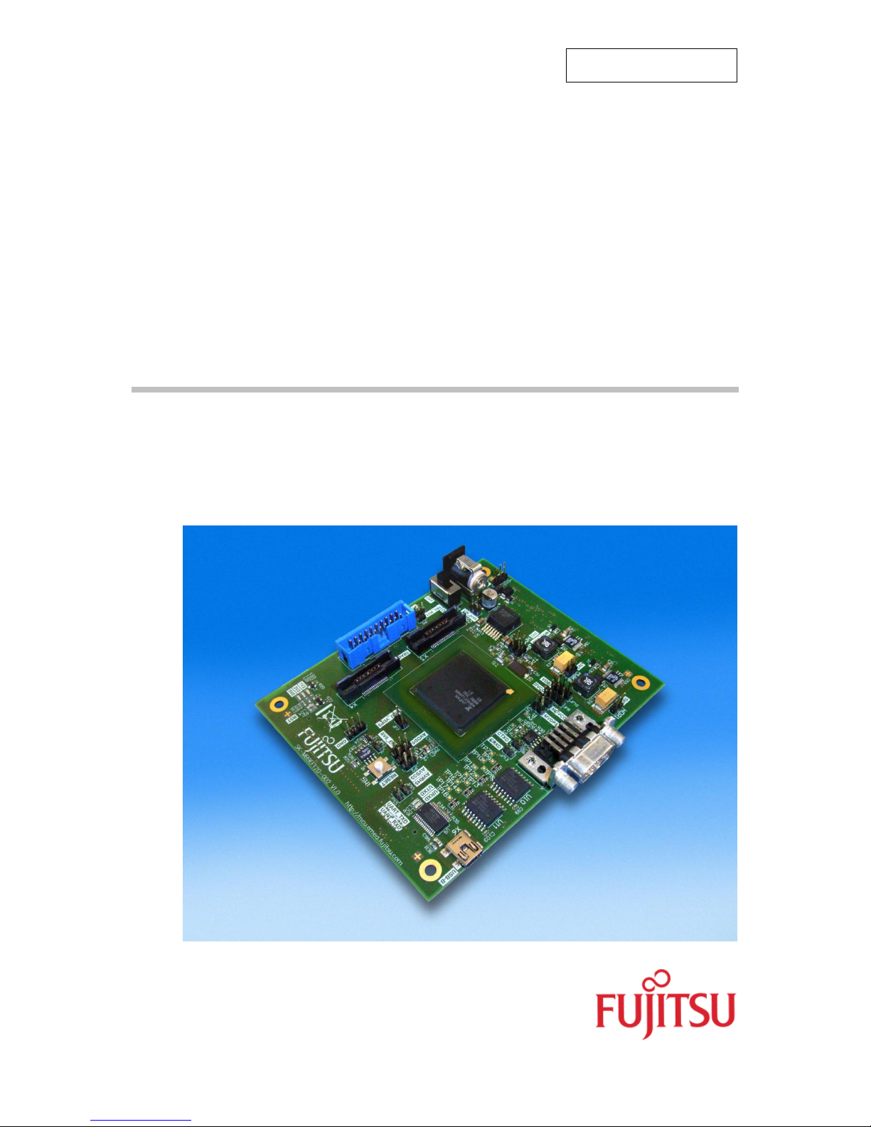
The SK-MB9EF120-002,-003 is a quick evaluation board for the Fujitsu FCR4 Cluster series flash
microcontroller MB96EF126 (Calypso). It can be used stand-alone for software development and
testing or as a simple target board to work with the emulator system.
Optionally, the adapter board ADA-FCR4-MULTIIO-001 is available as plug-under. It extends the
capabilities by additional interfaces and headers which provide easy access to the microcontroller
signals.
As an addition to the Multi-IO board, the ADA-FCR4-CLUSTER-001 is available. It provides a
complete automotive dashboard solution without separate microcontroller (all signals are controlled
from the SK-MB9EF126 microcontroller). It is connected to the Multi-IO board using a flat-cable.
1.2 Features
Supports Fujitsu’s MB9EF126 (Calypso) Series of microcontrollers
Variant STD: CPU soldered.
Variant SOCKET: CPU in BGA-socket.
12V external DC power supply (provided)
On-board 5V, 3V3 and 1V2 voltage regulators for I/O- and MCU supply
Light emitting diodes (LEDs) to monitor all regulated supply-rails
Selectable 5V and 3V3 voltage for specific digital (VDP5 and DVCC) and analogue (AVCC5 and
AVRH5) power domains
Reset-button and LED-indicator for reset
On-board voltage supply voltage supervisor
In-Circuit serial flash programming using the JTAG port
4MHz main crystal oscillator system-clocks.
32kHz crystal for sub clock operation (realtime clock, low-power operation)
All general purpose input/output (GPIO) pins not used on-board are available thru Board-to-Board
connectors on the bottom-side.
Both high-speed serial peripheral interface (SPI) ports (MCU, graphics-controller) are connected to
fast on-board Quad-SPI flash-devices.
Universal serial bus (USB) to serial converter (FT232R) connected to USART0 provides a serial
communication interface to a personal computer using a standard USB-A to Mini-B cable.
One controller area network (CAN) bus-interface on male d-sub-09 connector with industry-
standard pinout
Page 7

SK-MB9EF120-002,-003
Overview
© Fujitsu Semiconductor Europe GmbH - 7 -
UG-9E0010-11
ARM standard 20 pin IDC JTAG connector Trace-probe connector for up to 32-bit wide tracing Kit
contents
Starterkit-board.
USB-A to Mini-B cable.
Screws with spacers to mount onto a carrier-board or place on the table.
Page 8
SK-MB9EF120-002,-003
Hardware
UG-9E0010-11
- 8 - © Fujitsu Semiconductor Europe GmbH
2 Hardware
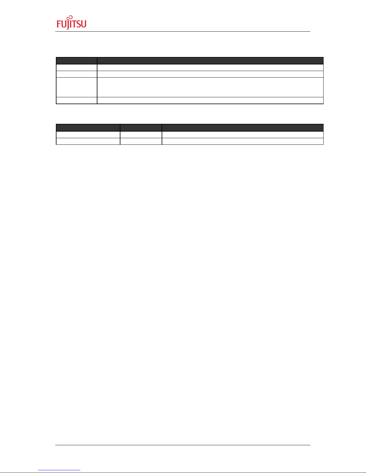
2.1 Printed Circuit Board (PCB) Overview
2.1.1 Top-View
A B C D E F G H I J K L M N O P Q R 1 1 2 2 3 3 4 4 5 5 6 6 7 7 8 8 9 9
10
10
11
11
12
12
13
13
14
14
15
15
16
16
17
17
A B C D E F G H I J K L M N O P Q R
Figure 2-1: PCB-Rev.1.1
U1: MCU – MB9EF126 (Calypso) Series in BGA320 package
Q2: 32768Hz RTC-crystal (SubClk)
Q1: 4MHz crystal for MainClk.
12V external DC power supply, 5V, 3V3 and 1V2 voltage regulators, S1 power switch
Power-LEDs for the 5V0, 3V3 and 1V2 power rails, SW1 Reset-button, Reset-LED
X2, X3, X4: debug and trace ports for ARM-standard connectors
Page 9
SK-MB9EF120-002,-003
Hardware
© Fujitsu Semiconductor Europe GmbH - 9 -
UG-9E0010-11
Serial Flashes (QSPI, MCU and GC)
USB (UART-emulation) and CAN (native) connectors
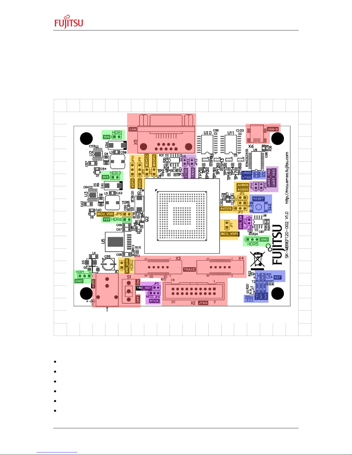
2.1.2 Bottom View
A B C D E F G H I J K L M N O P Q R 1 1 2 2 3 3 4 4
5
5
6 6 7
7
8
8
9 9 10
10
11
11
12
12
13
13
14
14
15
15
16
16
17
17
A B C D E F G H I J K L M N O P Q R
Figure 2-2: Bottom View PCB-Rev.1.1
J5, J6 - Board-to-Board connectors to Multi-IO
2.2 Power Supply
The power supply circuit consists of the input-stage and three voltage-regulators. The regulators are
switch-mode types (step-down).
Having the enables of the lower voltage supplies tied to the next higher voltage supply guarantees
correct sequencing in the order required (5V0 → 3V3 → 1V2). Power-down/disconnect of powerdomains and/or -rails is not supported.
All regulators are supplied from the input-rail Vin_prot (filtered input voltage, no regulator-staggering).
Page 10

SK-MB9EF120-002,-003
Hardware
UG-9E0010-11
- 10 - © Fujitsu Semiconductor Europe GmbH
Headers are connected to each voltage-rail to allow measuring the voltages. They should not be used
to power custom electronics. Each stage provides a header connected to connect to the
corresponding domain. Care must be taken when connecting to the 1V2-domain as noise on this rail
will have much more impact on this rail due to the low absolute voltage.
2.2.1 Input Stage
The power-supply connector is a standard DC-plug for an AC-adapter. Allowed input voltage ranges
from 9 to 12V, the adaptor should have a minimum power-rating of 12W (1A @ 12V).
After the power-switch, a reverse-voltage protection diode (D2) and an overvoltage protection device
(D3) follow. The latter suppresses/damps high voltage surges from the AC-adaptor which would
otherwise pass the following inductor and capacitors.
The inductor (L4) filters noise generated on-board, before it reaches the supply-cable which presents
a good antenna for EMI. Filtering incoming noise is a bonus.
2.2.2 I/O Supplies
The 5V0 and 3V3 supplies are generated from the input-rail by two step-down switching regulators,
each fixed to the desired output-voltage. As with all switching regulators, the designs are critical in
terms of switching noise.
Each regulator provides up to 3A to its rail.
2.2.3 MCU Core supply
The 1V2 supply for the MCU core is generated by a switching regulator module which includes the
inductor. It provides up to 3A to the rail.
2.2.4 Supply-Rail Monitor LEDs
Each supply-rail has its own LED-indicator. For the 1V2 rail, the LED is driven from the 3V3 rail, but
switched from the 1V2 rail.
All three rails are monitored for drops by a system-voltage supervisor (U6).
2.2.5 Power distribution
The three stabilized voltages drive the various MCU power-domains either directly (single-voltage
domains MCU_VDD, MCU_VDP3) or through a 3-pin jumper (dual-voltage domains VDP5, DVCC).
Additionally, there is a jumper before each domain's EMI-filter to allow injection of external supply or
measuring the current-consumption of the domain.
2.3 Reset
Board-Reset can be generated by basically two sources. Both are connected to the system-reset
which includes the microcontroller's reset-signal. Both sources can be disconnected from the resetnet by separate jumpers, thus excluding them from generating the reset-signal.
U6 generates the reset to the MCU and all other devices if one of the three system-voltages fails
(System Voltage Supervisor). It also monitors a push-button, generating a short reset-pulse (~100µs)
if this reset-button is pressed shortly. If the button is held pressed for some seconds, the reset-line will
be permanently asserted until the button is released. Caution: the SVS monitors the on-board
generated voltages, not the MCU power-domains. If any of the domains is supplied externally, it is left
to the user to provide a proper reset signal.
The second source of reset is the debugging-connectors (JTAG or TRACE). This source can also be
disconnected from the internal net.
A slight problem arises with the SVS output-signal having an internal current-source (pull-up) from the
3V3-domain. The MCU reset-input is located in the VDP5-domain, so an open-drain-driver (noninverting) is used which buffers the signal and has a pull-up resistor to VDP5 at the output, generating
RST_X_VDP5.
Page 11

SK-MB9EF120-002,-003
Hardware
© Fujitsu Semiconductor Europe GmbH - 11 -
UG-9E0010-11
RST_X_VDP5 also drives a LED which lights when the signal is active (low). On power-up or a press
of the reset-button, the LED will flash according to the pulse generated by the system voltage
supervisor. If the reset-button is pressed only for a short time, the pulse generated is too short to be
noticed by the eye (but it is sufficient for the hardware). Holding down the button for >~4s, generates
a permanent low-signal on reset until the button is released.
2.4 MCU Clocks
2.4.1 Main Clock
The MCU is clocked using its internal 4MHz crystal oscillator with Q1 as reference. As this is the main
clock reference, it controls all timing of the microcontroller when selected.
2.4.2 Sub-Clock (Real-Time Clock Oscillator)
Q2 is a 32.768kHz crystal connected to the microcontroller's real-time clock oscillator. This clock is
used to track time, while the other crystal oscillator is disabled.
2.5 On-Board Peripherals
The board provides two interfaces for external communication and two flash-devices for data-storage.
2.5.1 UART/USB-Serial Interface
Two port-signals (P0_45, P0_47) are connected to a USB-Serial converter chip (FT232R from FTDI).
The ports can be controlled by USART0, thus allowing a serial interface between the MCU and a PC.
For the FT232R, drivers exist for all major operating systems (OSX, Linux, Windows) wither built-in
(Linux) or for download (Windows). They provide a standard serial interface (“COM-port”/”ttyUSB”) to
the applications, so any terminal program can be used to transmit data between the MCU and a PC.
The interface does not provide hardware-handshake, thus it is left to the software to provide some
kind of flow-control and/or resynchronization, if necessary.
There is one LED per direction (RX, TX) signalling data-transmission.
The two ports can be disconnected from the converter by two jumpers, freeing them for other usage
(the two signals are also available on the B2B connector CN1).
The FT232R is powered from the USB-connector, making its operation independent on the power-
status of the board. However, as the supply of the serial interface I/O lines is powered from VDP5, the
voltages here always match the requirements of the connected port-signals.
2.5.2 CAN-Bus Interface
Two ports from the MCU (P0_20, P0_21) are connected to a CAN-Bus transceiver. The CAN-bus
itself is connected to a standard D-sub connector. The two signals are also RX and TX of the internal
CAN0-controller.
As with the UART, jumpers are available for each port to disconnect them from the interface, freeing
them for use from the B2B connector CN1.
2.5.3 Serial Flashes
There are two serial flash devices Spansion S25FL129P. One is connected to the MCU's HSSPI-port.
It provides data-storage for applications. The second flash is of the same type, but connects to the
GFXSPI-port which can be accessed by the graphics-controller without CPU intervention. The actual
device chosen supports Quad-SPI mode at up to 80MHz, resulting in a max. data rate of 40MB/s.
Page 12

SK-MB9EF120-002,-003
Hardware
UG-9E0010-11
- 12 - © Fujitsu Semiconductor Europe GmbH
2.6 Expansion Connectors
2.6.1 Board-to-Board (B2B) Connectors
On the bottom-side, there are two connectors (CN1, CN2). All MCU ports are available here, along
with power-supply and additional control-signals like reset.
Layout and placement of the SK-MB9EF120-002,-003 allow to plug a Fujitsu Multi-I/O board (ADAFCR4-MULTIIO-001) under the board, providing direct access to the ports via standard-raster
headers along with other features.
Alternatively, a custom PCB can be connected.
2.7 Debugging Facilities
The Starter-kit provides a JTAG-Interface on a 20-pin 2.54mm (0.1in) IDC-header for debugging. The
header uses the standard ARM configuration.
The second facility consists of two ARM-standard trace-connectors (X3, X4). While they can be used
together providing a 32-bit trace-port, the first (X3) can also be used solely with up to 16 trace-lines.
Having the JTAG-signals also available on X3, debugging does not require further connections.
Only one connector-set may be used at the same time: either X2 or X3/X4, because some signals are
shared between them. Debugging requires a conforming interface-adapter and corresponding
software on the host system.
Page 13

SK-MB9EF120-002,-003
Installation
© Fujitsu Semiconductor Europe GmbH - 13 -
UG-9E0010-11
3 Installation
3.1 First Contact
After opening the box, please check first if all parts are included. If any parts are missing, ask your
vendor.
The kit includes electrostatic sensitive devices. Unpacking should be done in an anti-static
environment.
After removing the packing-material, check all parts and especially the PCB for damages. Also check
the jumper-settings before initial powering up the board.
3.2 Engage
To power-up the board, first change the slider-switch (S1) to the “off”-position. Then connect the ACadapter to the AC-line. Connect the DC-plug to the board (X1), then turn on the slider-switch.
The AC-adaptor must provide 9-12V/12W DC. The positive (+) supply must be on the inner tip,
while the negative supply (-/GND) is on the outer ring. The power-input includes reversepolarity protection for an unlimited time and a protection against surges from the AC-adapter.
The latter must not be used as a voltage-regulator!
3.3 Lifesigns
After powering-up by turning on the power switch S1, the LED indicators for the supply-rails should
turn on without noticeable delay.
Additionally, the reset-LED flashes once, signalling release of the reset-signal by the voltage monitor.
If no LED lights op, turn off the power switch and check the polarity of the supply. If this is ok, or if
some power-LEDs are missing, flicker or show otherwise strange behaviour, check the power-rails for
shorts to GND and each other before retrying.
If the reset-LED flashes from time to time (maybe with a constant frequency), check if the powersupply used can satisfy the current requirements and measure the voltages on the power-rails. Most
times this occurs; one or multiple power-rails are at the edge of the SVS' trigger-level and drop below,
eg. if more current is drawn by a device.
Use HDR1-3 and 6 to measure voltages. Never short these Headers!
Page 14

SK-MB9EF120-002,-003
Configuration and Test-Points
UG-9E0010-11
- 14 - © Fujitsu Semiconductor Europe GmbH
4 Configuration and Test-Points
4.1 Jumpers
The SK-MB9EF120-002,-003 provides multiple options to access signals and configure its properties.
For this, it has two variants of jumpers:
(regular) Jumpers consist of two or three pin-headers and a small cap. They can be changed
without extra tools. They are used where changes are likely to occur. Wide jumpers use a 2.54mm
raster, while small jumpers use 2.00mm . The former are used for power-connections where also
measuring may be required, while the latter are sole configuration jumpers.
solder-jumpers change more basic options, the vast majority of applications do not require
changing them from their defaults. A solder-jumper is either a single 0R0 resistor or two resistors of
which only one may be placed. For the latter, a shared pad is often used to avoid placing both
resistors accidentally.
Name
Label
Description
Type
Default
Position
JP3
AVDD5
select ADC-supply:
1-2 = AVRH5
2-3 = VDP5
open = external
Caution: the ADC is an analog subsystem
and therefore sensitive to noise induced
from the power-supply lines.
3-pin wide
2-3
top N-8
JP2
AVRH5
open = access ADC VRH5 (reference
input).
Caution: the ADC is an analog subsystem
and therefore sensitive to noise induced
from the power-supply lines.
2-pin wide
closed
top N-7/8
JP1
AVSS5
open = access ADC VSS.
Caution: the APIX is an analog subsystem
and therefore sensitive to noise induced
from the power-supply lines.
2-pin wide
closed
top N-8
JP10
VDP5
select VDP5 supply-rail:
1-2 = 3V3 (3.3V on-board rail)
2-3 = 5V0 (5.0V on-board rail)
open = external
3-pin wide
2-3
top E/F-5/6
JP8
DVCC
select DVCC supply-rail:
1-2 = 3V3 (3.3V on-board rail)
2-3 = 5V0 (5.0V on-board rail)
open = external
3-pin wide
2-3
top F-5/6
JP6
MCU_VDD
open = access 1.2V supply for MCU.
2-pin wide
closed
top E-9
JP7
MCU_VDP3
open = access VDP3 domain for MCU.
2-pin wide
closed
top M-9/10
JP11
MCU_VDP5
open = access VDP5 domain for MCU.
2-pin wide
closed
top G-5/6
JP9
MCU_DVCC
open = access DVCC domain for MCU.
2-pin wide
closed
top G-5/6
JP4
RTCK-sel
enable/disable RTCK on JTAG:
1-2 = disable (pulled to GND)
2-3 = enable
open = invalid
see also solder-jumper R7
3-pin small
1-2
top G/H-15
JP5
TRC_RST
closed = enable resets from debug and
trace connector.
Quite likely not to be changed.
2-pin small
closed
top G/H-14/15
Page 15

SK-MB9EF120-002,-003
Configuration and Test-Points
© Fujitsu Semiconductor Europe GmbH - 15 -
UG-9E0010-11
Name
Label
Description
Type
Default
Position
JP12
SVS_EN
closed = enable resets from system-voltage
supervisor chip.
As the SVS also monitors the reset-button,
this also disables manual reset if open.
Quite likely not to be changed.
2-pin small
closed
top N/O-9/10
JP13
CAN_RXD
closed = connect RXD on CAN-Interface to
MCU-port P2_41
2-pin small
closed
top J-4/5
JP14
CAN_TXD
closed = connect TXD on CAN-Interface to
MCU-port P2_40
2-pin small
closed
top I/J-4/5
JP15
UART_RXD
closed = connect RXD on UART-Interface
to MCU-port P0_45
2-pin small
closed
top O/P-6/7
JP16
UART_TXD
closed = connect TXD on UART-Interface
to MCU-port P0_47
2-pin small
closed
top O-6/7
R1
RTCKfb
closed = enable RTCK
open to avoid disturbance on TCK line if
RTCK is not used. If operating on lower
frequencies, can be left connected if no
problems arise with TCK.
solder, 1R
closed
bottom K/L-7
On wide jumpers, the cap can be replaced by an ampere meter to measure current. However, care
must be taken to avoid inducing noise into the connected cables. Alternatively, if the cap is removed,
external power can be feed into the corresponding domain. Caution: do not back-drive current into
the supply-rails. Check the schematics before connecting an external power-supply to a
jumper's output pin (the pin which drives the power-domain). Double-check before powering
up!
DVCC, AVCC5 and VDP5 (see further description below) must be set to the same voltage-rail
when zero point detection (ZPD) on any of the SMC ports is to be used. Check the datasheet
for further requirements on the combination of voltages.
When using external supplies, the allowed voltages specified in the datasheet must be
observed. This also applies to the ports driven by the domains.
4.2 Headers
Headers are intended to access interesting points on the PCB. They may have the same sizes as
regular jumpers.
Name
Label
Description
Type
Position
HDR1
5V0
5.0V rail voltage measuring header.
Do not inject any current here!
2-pin wide
top D/E-2/3
HDR2
VIN_prot
Filtered and protected (against surges and reverse
polarity) input voltage. May be used to inject an
external supply.
2-pin wide
top E-13
HDR3
3V3
3.3V rail voltage measuring header.
Do not inject any current here!
2-pin wide
top D-6
HDR4, 5
GND
Access-points to the GND-plane. Can be used as
reference for scopes, logic-analyzers, voltmeters, etc.
3-pin wide
(each)
top B-14, O-11
HDR6
1V2
1.2V rail voltage measuring header.
Do not inject any current here!
2-pin wide
top E/F-9
Page 16

SK-MB9EF120-002,-003
Configuration and Test-Points
UG-9E0010-11
- 16 - © Fujitsu Semiconductor Europe GmbH
4.3 Test-Points
Testpoints are not for permanent connection, but mostly for failure-tracking. Normally, there is no
need to access them.
Name
Label
Description
Position
TP6
SubClk
input of 32768Hz crystal-oscillator (RTC, etc.).
top F-9
TP5
MainClk
main clock reference crystal (Q1).
top E/F-8
TP1
SYSC_CKOT
MCU-port P0_41 which can have this signal multiplexed on its
output.
top H/I-5/6
TP2
SYSC_CKOT
X
MCU-port P0_42 which can have this signal multiplexed on its
output.
top H-5/6
TP3
RTC_WOT
MCU-port P0_40 which can have this signal multiplexed on its
output.
top I-5/6
TP4
WDG_OBSER
VE
MCU-port P0_43 which can have this signal multiplexed on its
output.
top F-10
TP7
HSF_SCK
High-Speed QSPI interface (with flash)
top K-5
TP8
HSF_SS
top L-5
TP9
HSF_SIO0
top K-5
TP10
HSF_SIO1
top K/L-5
TP11
HSF_SIO2
top L-5
TP12
HSF_SIO3
top L-5
TP13
GXF_SCK
Graphics-Controller QSPI interface (with flash)
top L/M-5
TP14
GXF_SS
top M/N-5
TP15
GXF_SIO0
top M-5
TP16
GXF_SIO1
top M-5
TP17
GXF_SIO2
top N-5
TP18
GXF_SIO3
top N-5
The crystal testpoints TP5 and 6 are very sensitive to noise and load-factors, especially capacitive
loads can change the frequency dramatically. If possible, the clocks should be measured indirectly
using a high-speed timer or SYSC_CKOT.
4.4 Status Display
For user information, there are four LEDs on the board. Each power-rail (the supply generated onboard), is monitored by a single LED.
In addition, the reset-LED shows the status of the reset-line. For the default configuration and no
external reset (JTAG, button or from a plugged-under PCB), this is the status of the system-voltage
supervisor (SVS). It will be lit if any voltage-rail is out of its allowed limits.
Name
Color
Description (when lit)
Position
LD1
orange
5V0 rail up
top P-15
LD2
yellow
3V3 rail up
top O/P-15
LD3
green
1V2 rail up (driven by 3V3-rail)
top O-15
LD4
red
reset active
top O/P-14
Page 17

SK-MB9EF120-002,-003
Connectors
© Fujitsu Semiconductor Europe GmbH - 17 -
UG-9E0010-11
5 Connectors
The following table lists the location of all connectors on the board. The pin-out of each connector is
listed in separate sections.
Name
Type
Description
Position
CN1
SAMTEC QSH-090-01L-D-A
board-to-board connector. Allows to connect a Multi-IO board
or any other matching I/O-board.
bottom Q-4:13
CN2
SAMTEC QSH-090-01L-D-A
B2B, Further signals from the MCU.
bottom B-4:13
X2
2*10 2.54mm IDC
header (male)
Standard ARM 20pin debug-header with JTAG-interface.
Must not be connected at the same time as X3.
top H:M-15
X3,4
TYCO 5767054-1
38pin connector for standard ARM trace interface (16 bits).
Includes also JTAG. Must not be connected at the same time
as X2.
top F:N-13
X1
DC-plug
2.1mm pin DC plug for external power-supply.
top C/D-14:16
X5
9pin Dsub male
CAN-Bus connector with standard-pinout.
top F:J-1:4
X6
USB Mini-B plug
USB device-plug to connect a PC with USB-Serial protocol
driver.
top O/P-2/3
The two B2B connectors provide all MCU ports, power supplies and control-signals.
5.1 B2B Connectors (CN1, CN2)
These two connectors provide all signals to a plug-under board like the Multi-IO-Board. Signals
include all MCU ports as well as reset and power supplies from the SK-board.
Signals are always routed to these connectors, even if they are used on the SK-MB9EF120-002,-003
themselves. When using a signal on a plug-under board which is also connected to an on-board
peripheral or connector, it must be disconnected from the on-board resource by pulling the
corresponding jumper. Some signals can be disconnected separately, while other signals are
disconnected as a whole function-block.
Fitting mates for the other board are SAMTEC QTH type connectors.
5.1.1 CN1 Pinout
Special Signals
Pin(s)
Signal
Description
1,2,6,7,12,13,54,55,
65,66,97,98,101,102,109,110,113,
137,138,162,167,171,172,
Shield
GND
System Ground
3-5,8-11,14-53,67-96, 100, 119
n.c.
not connected
103,105,107
reserved
do not use
104,106,108
VDP5
VDP5 power domain
164,166,168,170
5V0
5.0V power rail
173,175,177,179
Vin
Raw input power (after the power-switch,
Page 18

SK-MB9EF120-002,-003
Connectors
UG-9E0010-11
- 18 - © Fujitsu Semiconductor Europe GmbH
Special Signals
Pin(s)
Signal
Description
but before any filter/protection. Should
not be used.
174, 176, 178, 180
Vin_prot
Vin after the filter. May be used to supply
SK-MB9DF120 from a plug-under board.
169
RST_X_VDP5
System-Reset. Open-Collector (pull-up
on SK-MB9DF120). input/output
MCU-Ports
Port
Pin
Pin
Port
Port
Pin
Pin
Port
55
56
P0_30
119
120
P0_52
P0_29
57
58
P0_45 P1_0
121
122
P1_4
P0_31
59
60
P0_47 P1_1
123
124
P1_5
P0_48
61
62
P0_20 P1_2
125
126
P1_6
P0_49
63
64
P0_21 P1_3
127
128
P1_7
65
66
P1_8
129
130
P1_12
67
68
P1_9
131
132
P1_13
69
70
P1_10
133
134
P1_14
71
72
P1_11
135
136
P1_15
73
74
137
138
75
76
P0_32
139
140
P0_8
77
78
P0_33
141
142
P0_9
79
80
P0_34
143
144
P0_10
81
82
P0_35
145
146
P0_11
83
84
P0_36
147
148
P0_12
85
86
P1_16
149
150
P0_13
87
88
P1_17
151
152
P0_14
89
90
P1_18
153
154
P0_15
91
92
P1_19
155
156
P0_40
93
94
P1_20
157
158
P0_41
95
96
P1_21
159
160
P0_42
97
98
P1_22
161
162
P0_24
99
100
P1_23
163
164
101
102
P0_43
165
166
103
104
167
168
105
106
169
170
107
108
171
172
109
110
173
174
P0_25
111
112
P0_22
175
176
113
114
P0_23
177
178
P0_44
115
116
P0_50
179
180
P0_46
117
118
P0_51
Page 19

SK-MB9EF120-002,-003
Connectors
© Fujitsu Semiconductor Europe GmbH - 19 -
UG-9E0010-11
5.1.2 CN2 Pinout
Special Signals
Pin(s)
Signal
Description
5,6,25,26,31,32,37,38,46,47,51,52,
65,66,71,72,77,78,83,84,89,90,95,96,
100,101,114,115,125,126,131,132,
137,138,143,144,149,150,155,156,
160-162,175,176, Shield
GND
System Ground
33-36,41-44, 49, 53-60, 61-64,
67-70,73-76,79-82,85-88,91-94,
7-99,102-113,119
n.c.
not connected
1-4,177-180
3V3
3.3V power rail.
MCU-Ports
Port
Pin
Pin
Port
Port
Pin
Pin
Port
P0_0 7 8
P0_1
95
96
P0_17 9 10
P0_27
97
98
P0_16
11
12
P0_26
99
100
P0_7
13
14
P0_19
101
102
P0_6
15
16
P0_18
103
104
P0_2
17
18
P0_37
105
106
P0_4
19
20
P0_28
107
108
P0_3
21
22
P0_39
109
110
P0_5
23
24
P0_38
111
112
25
26
113
114
P1_24
27
28
P1_27
115
116
P1_40
P1_25
29
30
P1_26 P1_32
117
118
P1_41
31
32
119
120
P1_31
33
34
P2_0
121
122
P2_2
35
36
P2_1
123
124
P2_3
37
38
125
126
P0_63
39
40
P0_62 P2_4
127
128
P2_6
41
42
P2_5
129
130
P2_7
43
44
131
132
P1_30
45
46
P2_8
133
134
P2_10
47
48
P1_28 P2_9
135
136
P2_11
49
50
P1_29
137
138
51
52
P2_12
139
140
P2_14
53
54
P2_13
141
142
P2_15
55
56
143
144
57
58
P2_16
145
146
P2_18
59
60
P2_17
147
148
P2_19
61
62
149
150
63
64
P2_20
151
152
P2_22
Page 20

SK-MB9EF120-002,-003
Connectors
UG-9E0010-11
- 20 - © Fujitsu Semiconductor Europe GmbH
MCU-Ports
Port
Pin
Pin
Port
Port
Pin
Pin
Port
65
66
P2_21
153
154
P2_23
67
68
155
156
69
70
P2_24
157
158
P1_39
71
72
P2_25
159
160
73
74
161
162
75
76
P1_48
163
164
P1_54
77
78
P1_49
165
166
P1_55
79
80
P1_50
167
168
P1_56
81
82
P1_51
169
170
P1_57
83
84
P1_52
171
172
P1_58
85
86
P1_53
173
174
P1_59
87
88
175
176
89
90
177
178
91
92
179
180
93
94
5.2 Debug Connector (X2)
This is an ARM-standard 20 pin JTAG connector.
Pin
Signal
Description
1
Vsns
Target voltage reference
2
VCCt
Target power
3
nTRST
JTAG TAP reset, active low
4
GND
Ground
5
TDI
JTAG Test Data In
6
GND
Ground
7
TMS
JTAG Test Machine State
8
GND
Ground
9
TCK
JTAG TAP Clock
10
GND
Ground
11
RTCK
Return TCK (optional)
12
GND
Ground
13
TDO
JTAG Test Data Out
14
GND
Ground
15
nRESET
Target reset, active low (system reset)
16
GND
Ground
17
DBREQ
Debug Request (not used)
18
GND
Ground
19
TVcc
Debug Acknowledge (not used)
20
GND
Ground
RTCK is deactivated by default. To enable it, a 0R0 resistor (soldering jumper, see there) must be
soldered. The feature is only required for high-speed clocking.
This connector must not be used at the same time as the trace-connector.
Page 21

SK-MB9EF120-002,-003
Connectors
© Fujitsu Semiconductor Europe GmbH - 21 -
UG-9E0010-11
5.3 Trace Connectors (X3, X4)
Much like the Debug-connector, this is also defined by ARM.
These connectors must not be used at the same time as the debug-connector.
5.3.1 Primary Trace-Connector (X3)
This can be used without X4, providing up an up to 16-bits trace-port.
Pin
Signal
Description
1-4, 10
NC
No connection
5, 30, 32
GND
Signal Ground
14, 34
VSUPPLY
Voltage Supply pin
12
VTREF
Target reference voltage
6
TRACECLK
Trace Clock pin
7
DBREQ
Probe Debug Request (unused)
8
DBACK
Probe Debug Acknowledge (unused)
9
nRESET
Target reset, active low
11
TDO
JTAG Test Data Out
13
RTCK
JTAG Return TCK (optional)
15
TCK
JTAG TAP Clock
16
TRACE7
Trace data
17
TMS
JTAG Test Machine State
18
TRACE6
Trace data
19
TDI
JTAG Test Data In
20
TRACE5
Trace data
21
nTRST
JTAG TAP Reset, active low
22
TRACE4
Trace data
23
TRACE15
Trace data
24
TRACE3
Trace data
25
TRACE14
Trace data
26
TRACE2
Trace data
27
TRACE13
Trace data
28
TRACE1
Trace data
29
TRACE12
Trace data
31
TRACE11
Trace data
33
TRACE10
Trace data
35
TRACE9
Trace data
36
TRACECTL
Trace Control
37
TRACE8
Trace data
38
TRACE0
Trace data
For the JTAG-signals see section 6.2 for details.
Page 22

SK-MB9EF120-002,-003
Connectors
UG-9E0010-11
- 22 - © Fujitsu Semiconductor Europe GmbH
5.3.2 Extension Trace-Connector (X4)
This connector extends the trace-bus width to 32-bits. It is the same type as X3.
Pin
Signal
Description
1-4, 6-11,
13-15, 17,
19, 21
NC
No connection
5, 30, 32,
36
GND
Signal Ground
34
VSUPPLY
Voltage Supply pin
12
VTREF
Target reference voltage
16
TRACE23
Trace data
18
TRACE22
Trace data
20
TRACE21
Trace data
22
TRACE20
Trace data
23
TRACE31
Trace data
24
TRACE19
Trace data
25
TRACE30
Trace data
26
TRACE18
Trace data
27
TRACE29
Trace data
28
TRACE17
Trace data
29
TRACE28
Trace data
31
TRACE27
Trace data
33
TRACE26
Trace data
35
TRACE25
Trace data
37
TRACE24
Trace data
38
TRACE16
Trace data
5.4 DC In Plug (X1)
This is a standard DC-Plug with inner pin (2.1mm dia) and outer shell. The connector is used to plug
an external DC power supply with 12V/1.5A DC to the evaluation board. Caution: the pin has positive
supply, while the shell is negative/GND.
Page 23

SK-MB9EF120-002,-003
Connectors
© Fujitsu Semiconductor Europe GmbH - 23 -
UG-9E0010-11
5.5 CAN-Bus Connector (X5)
This is a standard pin-out used for industrial CAN.
Pin
Signal
Description
1
NC
Not used
2
CANL
default low CAN-bus signal (inverted differential line)
3
GND
Ground
4
NC
Not used
5
NC
Not used
6
NC
Not used
7
CANH
default high CAN-bus signal (non-inverted differential line)
8
NC
Not used
9
NC
Not used
Shield
Shield
Tied to GND via 1M0||100nF
Check jumpers when using CAN to have the signals connected to the bus-driver. Also make sure the
related ports are not connected elsewhere via the B2B connectors.
5.6 USB-Serial Connector (X6)
Standard USB Mini-B Plug.
Pin
Signal
Description
1
VBUS
+5.0V Supply from Host. Powers the USB/Serial Converter FT232R
2
D-
inverted data-line
3
D+
non-inverted data-line
4
ID
leave open
5
GND
Reference-voltage
Shield
Shield
Tied to GND via 1M0||100nF
Check jumpers when using USB/UART to have the signals connected to the bus-driver. Also make
sure the related ports are not connected elsewhere via the B2B connectors.
Page 24

SK-MB9EF120-002,-003
Trouble shooting
UG-9E0010-11
- 24 - © Fujitsu Semiconductor Europe GmbH
6 Trouble shooting
Page 25

SK-MB9EF120-002,-003
Related Products
© Fujitsu Semiconductor Europe GmbH - 25 -
UG-9E0010-11
7 Related Products
SK-MB9DF120-001 Atlas MCU starterkit (with full atlas trace functionality)
SK-MB9DF120-002 Atlas MCU starterkit (QFP176 package, reduced trace
capability)
SK-MB9EF120-001 Calypso MCU starterkit (QFP296 package, replaced by this
SK-MB9EF120-002,-003)
SK-MB9EF120-003 See this description (socket variant).
ADA-FCR4-MULTIIO-001 Base board for using of MCU board with several IO
interfaces like CAN, LIN, MediaLB, Ethernet, Video and
Audio accessing
ADA-FCR4-CLUSTER-001 Automobile dashboard sample with stepper-motors and other
functions (requires Multi-IO board)
ADA-DISP2MULTIIO-001 Display-demonstration board for Multi-IO board.
Page 26

SK-MB9EF120-002,-003
Information on the Web
UG-9E0010-11
- 26 - © Fujitsu Semiconductor Europe GmbH
8 Information on the Web
Information about FUJITSU SEMICODUCTOR Products
can be found on the following Internet pages:
Microcontrollers (8-, 16- and 32bit), Graphics Controllers
Datasheets and Hardware Manuals, Support Tools (Hard- and Software)
http://mcu.emea.fujitsu.com/
Power Management Products
http://www.fujitsu.com/emea/services/microelectronics/powerman/index.html
For more information about FUJITSU SEMICODUCTOR
http://emea.fujitsu.com/semiconductor
Information about and software drivers for the peripheral devices used on the starter kit can be found
on the following Internet pages:
ARM architecture and software development tools
http://infocenter.arm.com
USB to serial converter
http://www.ftdichip.com
Power Supply and Monitoring
http://www.linear.com
http://www.national.com
CAN transceiver
http://www.infineon.com
Page 27

SK-MB9EF120-002,-003
Information on the Web
© Fujitsu Semiconductor Europe GmbH - 27 -
UG-9E0010-11
Quartz Crystal Units
http://www.ndk.com
http://www.microcrystal.ch
Flash Memory
http://www.spansion.com
Page 28

SK-MB9EF120-002,-003
EU-Konformitätserklärung / EU declaration of conformity
UG-9E0010-11
- 28 - © Fujitsu Semiconductor Europe GmbH
9 EU-Konformitätserklärung / EU declaration of conformity
Hiermit erklären wir,
Fujitsu Semiconductor Europe GmbH, Pittlerstrasse 47, 63225 Langen, Germany
dass dieses Board aufgrund seiner Konzipierung und Bauart sowie in den von uns in
Verkehr gebrachten Ausführung(en) den grundlegenden Anforderungen der EU-Richtlinie
2004/108/EC „Elektromagnetische Verträglichkeit“ entspricht. Durch eine Veränderung des
Boards (Hard- und/ oder Software) verliert diese Erklärung ihre Gültigkeit!
We,
Fujitsu Semiconductor Europe GmbH, Pittlerstrasse 47, 63225 Langen, Germany
hereby declare that the design, construction and description circulated by us of this board
complies with the appropriate basic requirements according to the EU Guideline
2004/108/EC entitled ’Electro-Magnetic Compatibility’. Any changes to the equipment
(hardware and/ or software) will render this declaration invalid!
Note:
All data and power supply lines connected to this starter kit should be kept as short as
possible, with a maximum allowable length of 3m. Shielded cables should be used for data
lines. As a rule of thumb, the cable length used when connecting external circuitry to the
MCU pin header connectors for example should be less than 20cm. Longer cables may
affect EMC performance and cause radio interference.
This evaluation board is a Class A product according to EN61326-1. It is intended to be
used only in a laboratory environment and might cause radio interference when used in
residential areas. In this case, the user must take appropriate measures to control and limit
electromagnetic interference.
Page 29

SK-MB9EF120-002,-003
China-RoHS regulation
© Fujitsu Semiconductor Europe GmbH - 29 -
UG-9E0010-11
10 China-RoHS regulation
This board is compliant with China RoHS.
Page 30

SK-MB9EF120-002,-003
Recycling
UG-9E0010-11
- 30 - © Fujitsu Semiconductor Europe GmbH
11 Recycling
Gültig für EU-Länder:
Gemäß der Europäischen WEEE-Richtlinie und deren Umsetzung in landesspezifische Gesetze
nehmen wir dieses Gerät wieder zurück.
Zur Entsorgung schicken Sie das Gerät bitte an die folgende Adresse:
Fujitsu Semiconductor Europe GmbH
Warehouse/Disposal
Monzastraße 4a
D-63225 Langen
Valid for European Union Countries:
According to the European WEEE-Directive and its implementation into national laws we take this
device back.
For disposal please send the device to the following address:
Fujitsu Semiconductor Europe GmbH
Warehouse/Disposal
Monzastraße 4a
D-63225 Langen
GERMANY
-- END --
 Loading...