

Page 1
Fujitsu Microelectronics Europe
User Guide
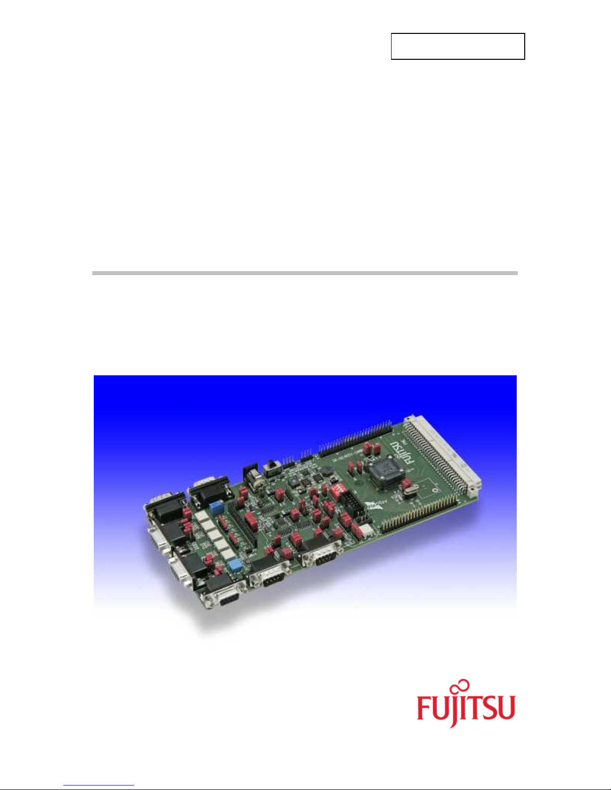
SK-91465X-100PMC
FMEMCU-UG-910056-11
MB91F465XA
EVALUATION BOARD
USER GUIDE
Page 2
SK-91465X-100PMC User Guide
Revision History
Revision History
Date Issue
2007-04-11 V1.0, MSt
Initial version
2008-09-05 V1.1, MSc, China-RoHS regulation added
This document contains 40 pages.
UG-910056-11 - 2 - © Fujitsu Microelectronics Europe GmbH
Page 3

SK-91465X-100PMC User Guide
Warranty and Disclaimer
Warranty and Disclaimer
To the maximum extent permitted by applicable law, Fujitsu Microelectronics Europe GmbH restricts
its warranties and its liability for the SK-91465X-100PMC and all its deliverables (eg. software
include or header files, application examples, target boards, evaluation boards, engineering samples
of IC’s etc.), its performance and any consequential damages, on the use of the Product in
accordance with (i) the terms of the License Agreement and the Sale and Purchase Agreement under
which agreements the Product has been delivered, (ii) the technical descriptions and (iii) all
accompanying written materials. In addition, to the maximum extent permitted by applicable law,
Fujitsu Microelectronics Europe GmbH disclaims all warranties and liabilities for the performance of
the Product and any consequential damages in cases of unauthorised decompiling and/or reverse
engineering and/or disassembling. Note, the SK-91465X-100PMC and all its deliverables are
intended and must only be used in an evaluation laboratory environment.
1. Fujitsu Microelectronics Europe GmbH warrants that the Product will perform substantially in
accordance with the accompanying written materials for a period of 90 days form the date of
receipt by the customer. Concerning the hardware components of the Product, Fujitsu
Microelectronics Europe GmbH warrants that the Product will be free from defects in material
and workmanship under use and service as specified in the accompanying written materials
for a duration of 1 year from the date of receipt by the customer.
2. Should a Product turn out to be defect, Fujitsu Microelectronics Europe GmbH´s entire liability
and the customer´s exclusive remedy shall be, at Fujitsu Microelectronics Europe GmbH´s
sole discretion, either return of the purchase price and the license fee, or replacement of the
Product or parts thereof, if the Product is returned to Fujitsu Microelectronics Europe GmbH in
original packing and without further defects resulting from the customer´s use or the transport.
However, this warranty is excluded if the defect has resulted from an accident not attributable
to Fujitsu Microelectronics Europe GmbH, or abuse or misapplication attributable to the
customer or any other third party not relating to Fujitsu Microelectronics Europe GmbH.
3. To the maximum extent permitted by applicable law Fujitsu Microelectronics Europe GmbH
disclaims all other warranties, whether expressed or implied, in particular, but not limited to,
warranties of merchantability and fitness for a particular purpose for which the Product is not
designated.
4. To the maximum extent permitted by applicable law, Fujitsu Microelectronics Europe GmbH´s
and its suppliers´ liability is restricted to intention and gross negligence.
NO LIABILITY FOR CONSEQUENTIAL DAMAGES
To the maximum extent permitted by applicable law, in no event shall Fujitsu
Microelectronics Europe GmbH and its suppliers be liable for any damages whatsoever
(including but without limitation, consequential and/or indirect damages for personal
injury, assets of substantial value, loss of profits, interruption of business operation,
loss of information, or any other monetary or pecuniary loss) arising from the use of
the Product.
Should one of the above stipulations be or become invalid and/or unenforceable, the remaining
stipulations shall stay in full effect
© Fujitsu Microelectronics Europe GmbH - 3 - UG-910056-11
Page 4

Contents
SK-91465X-100PMC User Guide
Contents
REVISION HISTORY............................................................................................................ 2
WARRANTY AND DISCLAIMER ......................................................................................... 3
CONTENTS.......................................................................................................................... 4
1 INTRODUCTION.............................................................................................................. 6
1.1 Abstract................................................................................................................... 6
1.2 Features.................................................................................................................. 6
1.3 General Description.................................................................................................7
1.3.1 MCU Clocks...............................................................................................7
1.3.2 MCU Operating Mode................................................................................7
1.3.3 FlexRay Physical Layer ............................................................................. 7
1.3.4 CAN Bus.................................................................................................... 7
1.3.5 RS-232 and LIN......................................................................................... 7
1.3.6 I²C ............................................................................................................. 7
1.3.7 MCU Pins ..................................................................................................8
1.3.8 User Buttons.............................................................................................. 8
1.3.9 User LEDs and optional LCD.....................................................................8
1.3.10 Power Supply ............................................................................................8
2 INSTALLATION...............................................................................................................9
2.1 Jumper Settings .................................................................................................... 10
2.2 Jumper Coordinates.............................................................................................. 12
3 JUMPERS AND SWITCHES.......................................................................................... 13
3.1 Operating Mode (S1)............................................................................................. 13
3.2 Power supply......................................................................................................... 14
3.2.1 Power switching by FlexRay physical layer.............................................. 15
3.3 Analogue Power Supply Voltage........................................................................... 16
3.4 UART”A” ............................................................................................................... 17
3.5 UART”B” / LIN “A” ................................................................................................. 17
3.6 UART ”C” / LIN “B”................................................................................................ 18
3.7 CAN “A”................................................................................................................. 19
3.8 CAN “B”................................................................................................................. 19
3.9 FlexRay “Channel A” (FR-A).................................................................................. 20
3.10 FlexRay “Channel B” (FR-B).................................................................................. 21
3.11 Reset-Generation.................................................................................................. 22
UG-910056-11 - 4 - © Fujitsu Microelectronics Europe GmbH
Page 5

SK-91465X-100PMC User Guide
Contents
3.12 Buttons SW1, SW2, SW3, SW4, SW5, SW6, SW7................................................23
4 PROGRAMMING THE INTERNAL FLASH.................................................................... 24
4.1 Asynchronous Mode..............................................................................................24
4.2 Synchronous Mode ............................................................................................... 26
5 CONNECTORS..............................................................................................................27
5.1 Power Connector (X13)......................................................................................... 27
5.2 Edge connector (X4, X5)....................................................................................... 27
5.3 UART / LIN Connector (X6, X8, X12) ....................................................................28
5.4 CAN Connector (X1, X2)....................................................................................... 29
5.5 FlexRay Connector (X3, X7).................................................................................. 29
5.6 USER-LEDs & optional LC-Display.......................................................................30
5.7 In-Circuit-Programming Connector (J4)................................................................. 31
5.8 VG96 connector (J1)............................................................................................. 32
6 SILK-PLOT OF THE BOARD ........................................................................................33
6.1 Silk-plot Top-side...................................................................................................33
6.2 Silk-plot bottom side.............................................................................................. 34
7 RELATED PRODUCTS ................................................................................................. 35
8 APPENDIX..................................................................................................................... 36
8.1 Tables...................................................................................................................36
8.2 Figures.................................................................................................................. 37
9 CHINA-ROHS REGULATION........................................................................................ 38
10 RECYCLING.................................................................................................................. 40
© Fujitsu Microelectronics Europe GmbH - 5 - UG-910056-11
Page 6

SK-91465X-100PMC User Guide
Chapter 1 Introduction
1 Introduction
1.1 Abstract
The SK-91465X-100PMC is a multifunctional evaluation board for the Fujitsu 32-bit FR60
Flash microcontroller series MB91F465XA.
It can be used stand-alone for software development and testing or as a simple target board
to work with the emulator system.
The board allows the designer immediately to start software development before his own
final target system is available.
1.2 Features
Supports Fujitsu's MB91F465XA MCU with embedded FlexRay interface in LQFP100
package
Can be used with the MB2198 Emulator System with the Socket Adapter Board
EMA-MB91F465X-NLS-100M20 and the Adapter Board EMA-MB91V460A-00x
together with the MB91V460A-100 FlexRay extension board
12V unregulated external DC power supply
5V and 3.3V onboard voltage regulators
Power-LEDs for all supply voltages
Onboard voltage supervisor monitors both supply voltages
In-Circuit serial Flash programming
All resources available for evaluation
All MCU pins routed to edge connectors
4 MHz main crystal
32 kHz crystal for sub clock operation
Two RS232 or LIN, one RS232, two CAN and two FlexRay interfaces (Channel A, B)
are usable simultaneously
Supports Power switching via FlexRay transceiver
8 User LEDs
optional: alphanumeric standard LC-Display connectable instead of LEDs
Reset button, Reset LED
6 User buttons
This board must only be used for test applications
in an evaluation laboratory environment.
UG-910056-11 - 6 - © Fujitsu Microelectronics Europe GmbH
Page 7

SK-91465X-100PMC User Guide
Chapter 1 Introduction
1.3 General Description
The SK-91F465X-100PMC supports the FUJITSU 32-bit Flash microcontroller
MB91F465XA.
The Starter Kit can be used as a stand-alone development platform, or with the emulation
system.
This User Guide is describing PCB version V1.1. The PCB version is printed at the TOP side
of the starter kit between Header X5 and MB91F465XA MCU [U1].
1.3.1 MCU Clocks
The board is supplied with a 4MHz crystal as the main oscillation clock for the MCU. Using
the internal PLL of the MCU, internal clock rates up to 100MHz can be achieved. The MCU
sub clock is connected to a 32.768 kHz crystal.
1.3.2 MCU Operating Mode
The operating mode of the microcontroller can be selected with the Dip-switch S1.
1.3.3 FlexRay Physical Layer
The connection to the physical layer of the FlexRay bus with 9-pin D-Sub connectors (X3
and X7) is realized with AMS8221B transceiver, it is also possible to deselect the termination
network connected to the channels. The transceivers provides differential transmit and
receive capability between FlexRay-controller and FlexRay-bus.
1.3.4 CAN Bus
Two high-speed CAN-transceivers (TLE6250GV33) are available to connect all available onchip CAN-controllers to 9-pin D-Sub connectors (X1 and X2). The transceivers provides
differential transmit and receive capability between CAN-controller and CAN-bus.
1.3.5 RS-232 and LIN
RS-232 and LIN signals are shared on the 9-pin D-Sub connectors (X8 and X12). It can be
selected, if RS-232 or LIN will be used. D-Sub X6 is connected to RS232.
Three RS-232 transceivers and two LIN transceivers are available, to connect the on-chip
USARTs to the 9-pin D-Sub connectors.
The RS-232 transceivers generate the adequate RS-232 levels for receive (RXD) and
transmit (TXD) lines. The RTS signal can be shortcut to CTS using jumpers (some PC
software needs this connection, when a 1:1 cable is used).
Either the DTR line or the RTS line of X1, X4 or X8 connectors can be selected to generate
a system reset.
The LIN transceivers (TLE7259) generate the adequate levels to drive the bus line in LINsystems for automotive and industrial applications.
1.3.6 I²C
Two additional pull-up resistors R24 and R25 can be connected to the I²C bus lines by
setting the according Jumpers (JP18, JP22).
© Fujitsu Microelectronics Europe GmbH - 7 - UG-910056-11
Page 8

SK-91465X-100PMC User Guide
Chapter 1 Introduction
1.3.7 MCU Pins
All pins of the microcontroller except the oscillator pins X0/1(A) are connected to the edge
connectors X4 and X5 and are directly available to the user. Furthermore, most signals are
available on the VG96 connector J1.
1.3.8 User Buttons
There are five push buttons on board, which can be connected to input-ports of the
microcontroller. Some ports may support additional functions like external interrupts (INT0,
INT1 and INT2), trigger for the Reload Timer or Input-Capture (TIN0 / ICU0, TIN2 / ICU2)
and analogue trigger (ATGX). Button SW7 issues a local wake up request to the Flexray
physical layers (AMS8221B). One additional button is reserved as System-Reset-button to
reset the MCU, but it is possible to disconnect the RST-port with JP14.
1.3.9 User LEDs and optional LCD
Eight user-LEDs are connected via two pull-down resistor networks to port P27_D0 P27_D3 and to port P16_D0 - P16_D3. Parallel to the LEDs, the connector J2 can be used
to connect a standard alphanumeric display. The resistor networks RN1 and RN2 can be
removed, to free the ports.
1.3.10 Power Supply
The on-board step-down switching regulators allow the user to connect an unregulated DC
input voltage of +12V (max. 2600 mA) to the starter-kit. The switching regulator provide the
voltages of 5V (1.6A), 3.3V (1.6A) on the starter kit. The switching regulators are short circuit
protected and provide a thermal shutdown.
UG-910056-11 - 8 - © Fujitsu Microelectronics Europe GmbH
Page 9

SK-91465X-100PMC User Guide
Chapter 2 Installation
2 Installation
Remove the board carefully from the shipping carton.
First check if there are any damages before power on the starter kit.
To supply the starter kit, use the delivered In-Plug AC-DC Adapter (UPA 2000). Select the
AC plug adapter suitable for your country power sockets
Figure 2-1: AC plug adapter
and insert this adapter into the connection terminal on the AC-DC adapter.
Figure 2-2: AC plug adapter selection
Check the selected output DC voltage of the AC-DC In-Plug adapter at the voltage selection
key. It should be 12V! Change the output voltage only in a powered-down condition!
Figure 2-3: DC voltage selection
Select the low voltage adapter suitable to the power connector X13 at the SK-91465X100PMC and plug it to the connecting socket in the right orientation (+ connected to shield
and GND connected to centre pin).
Figure 2-4: Low voltage adapter selection
© Fujitsu Microelectronics Europe GmbH - 9 - UG-910056-11
Page 10
SK-91465X-100PMC User Guide
Chapter 2 Installation
Now connect the DC low voltage adapter to the Starter kit and plug in the In-Plug Power
Supply to a power socket. The SK-91465X-100PMC can be turned on with the on board
power switch S2.
For the power supply of the SK-91465XA-100PMC a DC input voltage of 12V is
recommended. The positive voltage (+) must be connected to the shield, and ground
(GND) must be connected to the centre of the connector X13!
After power-on of the SK-91465X-100PMC, the two red power-on LEDs D25 (5V) and D24
(3.3V) should be light. The LED D10 should light and the reset LED D1 should be off.
2.1 Jumper Settings
Jumper Description / Function Type
JP1 CAN A (TXD) / CAN4 Solder JP 3 pin
JP2 AVcc Jumper 2 pin Closed J22
JP3 AVcc=AVRH Jumper 2 pin Closed J22
JP4 SW1 (INT0) Jumper 2 pin Closed H10
JP5 RX CAN A / CAN4 Jumper 2 pin Closed J6
JP6 SW2 (INT1) Jumper 2 pin Closed H10
JP7 AVss Jumper 2 pin Closed J22
JP8 TX CAN A / CAN4 Jumper 2 pin Closed K6
JP9 SW3 (ATGX) Jumper 2 pin Closed G10
JP10 SW4 (TIN0) Jumper 2 pin Closed G10
JP11 CAN B (TXD) / CAN0 Solder JP 3 pin
JP12 SW5 (TIN2) Jumper 2 pin Closed G10
JP13 Reset immediate / delayed Solder JP 3 pin
JP14 RESET Jumper 2 pin Closed F9 / F8
JP15 RX CAN B / CAN0 Jumper 2 pin Closed K11
JP16 TX CAN A / CAN4 Jumper 2 pin Closed K11
JP17 X3 Shield – pin 5 (FlexRay B) Jumper 2 pin Open E15
JP18 SDA0 Pull-up Jumper 2 pin Open H21
JP19 INH1 / INH2 FlexRay Channel A Jumper 3 pin 1-2 F11
JP20 BM-B termination Jumper 2 pin Closed E14
JP21 BP-B termination Jumper 2 pin Closed E13
JP22 SCL0 Pull-up Jumper 2 pin Open H21
JP23 X3 - GND / network Jumper 3 pin 1-2 E15
JP24 RTS-CTS A Jumper 2 pin Open E5
JP25 INH / Vin Jumper 3 pin 1-2 H16
JP26 UART A (RXD) / UART4 Jumper 2 pin Closed F14
JP27 INHxA / INHxB Jumper 4 pin Closed H16
JP28 DTR/RTS A Jumper 3 pin Open E5
JP29 UART A (TXD) / UART4 Jumper 2 pin Closed F14
JP30 X7 Shield – pin 5 (FlexRay A) Jumper 2 pin Open E11
JP31 INH1 / INH2 FlexRay Channel B Jumper 3 pin 1-2 E15
JP32 LIN A Master-Mode Jumper 2 pin Open H12
JP33 DTR / DTRx Jumper 3 pin Open H15
JP34 BM-A termination Jumper 2 pin Closed E10
JP35 “WAKE” LIN-transceiver, LIN A Solder JP 3 pin
JP36 BP-A termination Jumper 2 pin Closed E9
Default
Setting
1-2 J5
1-2 J10
1-2 E7
1-2 G12
Coordinates
UG-910056-11 - 10 - © Fujitsu Microelectronics Europe GmbH
Page 11
SK-91465X-100PMC User Guide
Chapter 2 Installation
Jumper Description / Function Type
JP37 LIN A enable Jumper 2 pin Open G11
JP38 VBAT LIN A Jumper 2 pin Open E5
JP39 X7 - GND / network Jumper 3 pin 1-2 E11
JP40 TX (UART B) / BUS (LIN A) Jumper 3 pin 2-3 F5
JP41 STBN-A Jumper 3 pin 1-2 F12
JP42 RXD (UART B / LIN A) UART7 Jumper 3 pin 1-2 G13
JP43 STBN-B Jumper 3 pin 1-2 F16
JP44 TXD (UART B / LIN A) UART7 Jumper 3 pin 1-2 G13
JP45 TXD FlexRay A Jumper 2 pin Closed E12
JP46 TXEN FlexRay A Jumper 2 pin Closed E12
JP47 ERRN-A Jumper 2 pin Open F12
JP48 RXD FlexRay A Jumper 2 pin Closed F12
JP49 RTS-CTS B Jumper 2 pin Open F5
JP50 DTR/RTS B Jumper 3 pin Open F5
JP51 ERRN-B Jumper 2 pin Open F16
JP52 V_ALL Jumper 2 pin Closed H16
JP53 C-pin Solder JP 2 pin Closed G22
JP54 LIN B Master-Mode Jumper 2 pin Open J12 / K12
JP55 V_MCU Jumper 2 pin Closed H20
JP56 “WAKE” LIN-transceiver, LIN B Solder JP 3 pin
JP57 LIN B enable Jumper 2 pin Open J12
JP58 TXD FlexRay B Jumper 2 pin Closed E16
JP59 TXEN FlexRay B Jumper 2 pin Closed E16
JP60 VBAT LIN B Jumper 2 pin Open H5
JP61 EN-A Jumper 3 pin 1-2 E13
JP62 RXD FlexRay B Jumper 2pin Closed E16
JP63 Vcc (5V / 3.3V) Jumper 3 pin 1-2 H15 / H16
JP64 VDD5R (V_ALL / 3.3V) Jumper 3 pin 1-2 H20
JP65 TX (UART C) / BUS (LIN B) Jumper 3 pin 2-3 H5
JP66 EN-B Jumper 3 pin 1-2 E16
JP67 RXD (UART B / LIN A) UART6 Jumper 3 pin 1-2 J13
JP68 TXD (UART B / LIN A) UART6 Jumper 3 pin 1-2 J13
JP69 RTS-CTS C Jumper 2 pin Open J5
JP70
JP71 DTR/RTS C Jumper 3 pin Open J5
JP72 RESET UART A/B/C Jumper 6 pin Open G14
JP73 Clock BNC X0/Pin16 Solder JP 3 pin
JP74 X14 / X1 Solder JP 2 pin Closed F22
JP75 X14 / X0 Solder JP 2 pin Closed F22
WAKE-A (1-2)
WAKE-B (3-4)
Jumper 4 pin Closed D16
Default
Setting
1-2 J12
Open F22
Coordinates
© Fujitsu Microelectronics Europe GmbH - 11 - UG-910056-11
Table 2-1: Default jumper settings
Page 12
2.2 Jumper Coordinates
UART “C“
UART “B“ /
CAN
“A”
FlexRay
UART
“A”
FlexRay
CAN
“B”
A B C D E F G H J K L M N
SK-91465X-100PMC User Guide
Chapter 2 Installation
1
2
3
4
5
6
7
8
9
10
11
12
13
14
15
16
1
2
LIN“B“
UART7
LIN“A“
UART6
3
4
5
UART4
CAN4
6
7
8
Channel A
9
CAN0
10
11
12
13
Channel B
14
15
16
17
18
19
20
21
22
23
24
25
26
27
17
18
19
20
21
22
23
24
25
26
27
A B C D E F G H J K L M N
Figure 2-5: Jumper Coordinates
UG-910056-11 - 12 - © Fujitsu Microelectronics Europe GmbH
Page 13

SK-91465X-100PMC User Guide
1 2 3 4
MD0 MD1 MD2 nc
Chapter 3 Jumpers and Switches
3 Jumpers and Switches
This chapter describes all jumpers and switches that can be modified on the evaluation
board. The default setting (MB91F465XA Series) is shown with a grey shaded area.
3.1 Operating Mode (S1)
The DIP-switch S1 is used to set the operating mode of the MCU. Ensure that the mode pin
settings correspond to the operation-mode of the application. For more detailed information
please check the Hardware-Manual of the microcontroller.
DIP switch Setting Logical value
S1/1 (MD0)
ON (closed) 1 (high)
OFF (open) 0 (low)
ON (closed) 1 (high)
S1/2 (MD1)
OFF (open) 0 (low)
ON (closed) 1 (high)
S1/3 (MD2)
OFF (open) 0 (low)
S1/4 not connected
Default: grey
Table 3-1: MCU operating mode
Dip-Switch S2
(default setting)
ON
OFF
© Fujitsu Microelectronics Europe GmbH - 13 - UG-910056-11
Figure 3-1: MCU Mode Switch
Page 14

SK-91465X-100PMC User Guide
Chapter 3 Jumpers and Switches
3.2 Power supply
The onboard voltage regulator (U9) provide stabilized 5V and 3.3V supplies to the MCU and
peripherals. Even though they are thermally protected against overload, care must be taken
when supplying current for additional circuitry.
The LIN Vs line can be connected directly to the input supply of the board by JP40 and
JP60. In this case, the input voltage to the board has to be suitable for the connected bus
devices (mostly around 12V). Since there is a protection diode between Vin and Vs, it is not
possible to power the board over the LIN bus.
JP63 Selects the MCU IO and peripherals Vcc voltage (V_ALL = 3.3V or 5V)
JP64 Selects the MCU Core voltage regulator input voltage (3.3V / V_ALL)
JP52 Connects the Board voltage to V_ALL. Can be used for current measurement of
whole board.
JP55 Connects the MCU Io voltage (V_MCU) to V_ALL. Can be used for current
measurement of MCU.
JP25 Selects the Gate input voltage of MOSFET Q2 (Vin / INHx)
JP40 Connects Vs (Pin 1 of X8) to Vin
JP60 Connects Vs (Pin 1 of X12) to Vin
JP1 Selects Vcc of CAN A (Pin 3 of U2) (5V or V_ALL)
JP11 Selects Vcc of CAN B (Pin 3 of U4) (5V or V_ALL)
Jumper Setting Description
1 - 2 MCU / Peripherals @ 5V (Vcc) JP63
(Vcc 5V / 3V)
JP64
(VDD5R
3V/V_ALL)
2 - 3 MCU / Peripherals @ 3.3V (Vcc)
1 - 2 Supply to Core voltage regulator same as JP63
selection(V_ALL)
2 - 3 Supply to Core voltage regulator is 3.3V
Closed Power supply VBoard connected to V_ALL JP52
(V_ALL)
Open Power supply VBoard not connected to V_ALL
Closed Power supply V_ALL connected to V_MCU JP55
(V_MCU)
Open Power supply V_ALL not connected to V_MCU
1-2 Gate of MOSFET (Q2) connected to Vin
JP25
2-3 Gate of MOSFET (Q2) connected to INH pin of
FlexRay transceiver (X9, X1)
(Vin_A)
JP60
(Vin_B)
UG-910056-11 - 14 - © Fujitsu Microelectronics Europe GmbH
Closed Vs of LIN A is powered by the board (Vin) JP40
Open No voltage supply to Vs of LIN A
Closed Vs of LIN B is powered by the board (Vin)
Open No voltage supply to Vs of LIN B
Page 15

SK-91465X-100PMC User Guide
Chapter 3 Jumpers and Switches
Jumper Setting Description
JP1
(CAN A Vcc)
1 - 2 Vcc of CAN A is supplied with 5V
2 - 3 Vcc of CAN A is supplied with V_ALL
1 - 2 Vcc of CAN B is supplied with 5V JP11
(CAN B Vcc)
2 - 3 Vcc of CAN B is supplied with V_ALL
Default: grey
Table 3-2: Power supply jumper settings
Power measurements:
Via JP52 it is possible to measure the power consumption of the whole board.
Via JP55 the consumption of MCU Vcc pins can be measured.
For VDD5R consumption measurements JP64 must be used.
3.2.1 Power switching by FlexRay physical layer
This board supports power switching by FlexRay physical layer (X9, X11).
For this reason the Vcc voltage (Selected by JP63) is controlled by a MOSFET (Q2).
12V level at the Gate pin will pass the Vcc voltage to the board. Connecting 0V at the Gate
pin the MOSFET (Q2) switch off the Vcc power supply of the board.
JP25 selects if Vin (12V) or the FlexRay physical layer INHx pins are connected to the Gate
pin. JP27 selects if INHx pin of FlexRay Physical layer channel A or channel B is used for
power switching. JP19 and JP31 selects if INH1 or INH2 pins (channel A / B).
Jumper Setting Description
1-2 Gate of MOSFET (Q2) connected to Vin
JP25
2-3
Gate of MOSFET (Q2) connected to INH pin
of FlexRay transceiver (X9, X1)
1-2 INHx-A connected to JP25
JP27
3-4 INHx-B connected to JP25
1-2 Select Channel A INH1
JP19
2-3 Select Channel A INH2
1-2 Select Channel B INH1
JP31
2-3 Select Channel B INH2
Default: grey
Table 3-3: Jumper Settings FlexRay power switching
© Fujitsu Microelectronics Europe GmbH - 15 - UG-910056-11
Page 16

SK-91465X-100PMC User Guide
Chapter 3 Jumpers and Switches
3.3 Analogue Power Supply Voltage
The power supply as well as the positive reference voltage for the A/D-converter can be
provided internally or externally.
JP2, JP8 connects analogue power supply voltages (AVcc and AVss)
JP3 connects the analogue reference voltage AVRH to AVcc
Jumper Setting Description
Closed AVcc is connected to Vcc
JP2 (AVcc)
Open AVcc is disconnected from Vcc
Closed AVRH is connected to AVcc
JP3 (AVRH)
Open AVRH defined by resistor network*1
Closed AVss is connected to GND
JP7 (AVss)
Open AVss is disconnected from GND
Default: grey
Table 3-4: Jumper settings for Analogue Power supply
*1
By default the resistor network (R8, R11) is not mounted on the board
By default, the A/D-converter supply and reference voltage is same as the microcontroller
supply voltage.
Note:
If JP2 and JP7 are open, the user has to supply an
adequate analogue voltage supply (AVcc and AVss) to
the A/D-converter.
If JP3 is open, the resistors R8 and R11 define AVRH.
By default the resistor network (R8, R11) is not
mounted on the board.
UG-910056-11 - 16 - © Fujitsu Microelectronics Europe GmbH
Page 17

SK-91465X-100PMC User Guide
Chapter 3 Jumpers and Switches
3.4 UART”A”
One RS232-transceiver (U5, X6) can be connected to one of the microcontroller’s UART
interfaces.
JP26, JP29 connect UART 3 to the RS232-transceiver (U1, X3)
JP24 Some programs (e.g. Terminals) need a connection between CTS and RTS
Jumper Setting Description
JP26 (UART”A”RxD)
Closed SIN4 of the MCU is connected to UART”A”
Open SIN4 of the MCU is not connected to UART”A”
JP29 (UART”A”TxD)
Closed SOT4 of the MCU is connected to UART”A”
Open SOT4 of the MCU is not connected to UART”A”
Closed RTS and CTS of X6 are connected
JP24 (RTS-CTS)
Open RTS and CTS of X6 are not connected
Default: grey
Table 3-5: UART “A” jumper settings
3.5 UART”B” / LIN “A”
One RS232-transceiver (U7) or one LIN-transceiver (U6) can be connected to one of the
microcontroller’s UART interfaces. Connect to D-Sub X8 corresponding RS232 or LIN cable.
By default RS232 is selected to X8.
JP42 Selects if RS232 or LIN is connected to SIN7 of MCU
JP44 Selects if RS232 or LIN is connected to SOT7 of MCU
JP40 Selects if UARTB or LINA is connected to pin2 of X8
JP49 Some programs (e.g. Terminals) need a connection between CTS and RTS
JP37 Enable LIN-Transceiver
JP32 Selects LIN Master mode
JP38 Connects Vs (Pin 1 of X8) to Vin
Jumper Setting Description
JP42
(UART B / LIN A)
JP44
(UART B / LIN A)
1-2 SIN7 of the MCU is connected to U7 (RS232)
2-3 SIN7 of the MCU is connected to U6 (LIN)
1-2 SOT7 of the MCU is connected to U7 (RS232)
2-3 SOT7 of the MCU is connected to U6 (LIN)
1-2 BUS Signal (LINA) is connected to pin2 of X8 JP40
(X8 pin2)
2-3 Tx Signal (UARTB) is connected to pin2 of X8
Closed RTS and CTS of X8 are connected JP49
(RTS-CTS)
© Fujitsu Microelectronics Europe GmbH - 17 - UG-910056-11
Open RTS and CTS of X8 are not connected
Page 18

SK-91465X-100PMC User Guide
Chapter 3 Jumpers and Switches
Jumper Setting Description
Closed LIN-transceiver is enabled JP37
(LIN A enable)
Open LIN-transceiver is disabled
Closed LIN Master-mode JP32
(LIN A Master)
Open LIN Slave-mode
Closed Vs of LIN B is powered by the board JP38
(VBAT_A)
Open No voltage supply to Vs of LIN B
Default: grey
Table 3-6: UART “B”/ LIN “A” jumper settings
3.6 UART ”C” / LIN “B”
One RS232-transceiver (U10) or one LIN-transceiver (U8) can be connected to one of the
microcontroller’s UART interfaces. Connect to D-Sub X12 corresponding RS232 or LIN
cable. By default RS232 is selected to X12.
JP67 Selects if RS232 or LIN is connected to SIN6 of MCU
JP68 Selects if RS232 or LIN is connected to SOT6 of MCU
JP65 Selects if UARTC or LINB is connected to pin2 of X12
JP69 Some programs (e.g. Terminals) need a connection between CTS and RTS
JP57 Enable LIN-Transceiver
JP54 Selects LIN Master mode
JP60 Connects Vs (Pin 1 of X12) to Vin
Jumper Setting Description
JP67
(UART C / LIN B)
JP68
(UART C / LIN B)
1-2 SIN6 of the MCU is connected to U10 (RS232)
2-3 SIN6 of the MCU is connected to U8 (LIN)
1-2 SOT6 of the MCU is connected to U10 (RS232)
2-3 SOT6 of the MCU is connected to U8 (LIN)
1-2 BUS Signal (LINB) is connected to pin2 of X12 JP65
(X12 pin2)
2-3 Tx Signal (UARTC) is connected to pin2 of X12
Closed RTS and CTS of X12 are connected JP69
(RTS-CTS)
Open RTS and CTS of X12 are not connected
Closed LIN-transceiver is enabled JP57
(LIN B enable)
Open LIN-transceiver is disabled
Closed LIN Master-mode JP54
(LIN B Master)
UG-910056-11 - 18 - © Fujitsu Microelectronics Europe GmbH
Open LIN Slave-mode
Page 19

SK-91465X-100PMC User Guide
Chapter 3 Jumpers and Switches
Jumper Setting Description
Closed Vs of LIN B is powered by the board JP60
(VBAT_B)
Open No voltage supply to Vs of LIN B
Default: grey
Table 3-7: UART “C”/ LIN “B” jumper settings
3.7 CAN “A”
One high-speed CAN-transceiver can be connected to the microcontroller’s CAN interface.
JP5, JP8 connects a CAN-port to the CAN-transceiver (U2, X1).
If the CAN interface is not used then the jumpers should be left open.
Jumper Setting Description
JP5 (CAN”A”RxD)
JP8 (CAN”A”TxD)
Default: grey
Closed RX4 of the MCU is connected to CAN”A” (X1)
Open RX4 of the MCU is not connected to CAN”A”
Closed TX4 of the MCU is connected to CAN”A” (X1)
Open TX4 of the MCU is not connected to CAN”A”
Table 3-8: CAN “A” jumper settings
3.8 CAN “B”
One high-speed CAN-transceiver can be connected to the microcontroller’s CAN interface.
JP15, JP16 connects a CAN-port to the CAN-transceiver (U4, X2).
If the CAN interface is not used then the jumpers should be left open.
Jumper Setting Description
JP15 (CAN”B”RxD)
JP16 (CAN”B”TxD)
Default: grey
Closed RX0 of the MCU is connected to CAN”B” (X2)
Open RX0 of the MCU is not connected to CAN”B”
Closed TX0 of the MCU is connected to CAN”B” (X2)
Open TX0 of the MCU is not connected to CAN”B”
Table 3-9: CAN “B” jumper settings
© Fujitsu Microelectronics Europe GmbH - 19 - UG-910056-11
Page 20

SK-91465X-100PMC User Guide
Chapter 3 Jumpers and Switches
3.9 FlexRay “Channel A” (FR-A)
One FlexRay transceiver (X9, X7) can be connected to one of the microcontroller’s FlexRay
interface (one channel). In addition further pins of the MCU can be connected to the FlexRay
transceiver for Error-read out feature and power supply switching.
JP45 Connects FlexRay transceiver TXD pin to microcontroller FlexRay TXDA pin
JP46 Connects FlexRay transceiver TXEN pin to microcontroller FlexRay TXENA pin
JP48 Connects FlexRay transceiver RXD pin to microcontroller FlexRay RXDA pin
JP41 Selects FlexRay transceiver STBN pin to Vio or microcontroller pin.
JP61 Selects FlexRay transceiver EN pin to Vio or microcontroller pin.
JP47 Connects FlexRay transceiver ERRN pin to microcontroller pin.
Jumper Setting Description
JP45
(TXDA)
JP46
(TXENA)
JP48
(RXDA)
JP41
(STBN-A)
JP61
(EN-A)
JP47
(ERRN-A)
Default: grey
Closed TXDA of the MCU is connected to FR-A
Open TXDA of the MCU is not connected to FR-A
Closed TXENA of the MCU is connected to FR-A
Open TXENA of the MCU is not connected to FR-A
Closed
Open
1-2
2-3
1-2
2-3
Closed
Open
RXDA of the MCU is connected to FR-A
RXDA of the MCU is not connected to FR-A
STBN of the FR-A is connected to Vio-A.
STBN of the FR-A is connected to MCU pin.
EN of the FR-A is connected to Vio-A.
EN of the FR-A is connected to MCU pin.
ERRN of the FR-A is connected to MCU pin.
ERRN of the FR-A is not connected to MCU pin.
Table 3-10: FlexRay “Channel A” jumper settings
UG-910056-11 - 20 - © Fujitsu Microelectronics Europe GmbH
Page 21

SK-91465X-100PMC User Guide
Chapter 3 Jumpers and Switches
3.10 FlexRay “Channel B” (FR-B)
One FlexRay transceiver (X11, X3) can be connected to one of the microcontroller’s FlexRay
interface (one channel). In addition further pins of the MCU can be connected to the FlexRay
transceiver for Error-read out feature and power supply switching.
JP58 Connects FlexRay transceiver TXD pin to microcontroller FlexRay TXDA pin
JP59 Connects FlexRay transceiver TXEN pin to microcontroller FlexRay TXENA pin
JP62 Connects FlexRay transceiver RXD pin to microcontroller FlexRay RXDA pin
JP43 Selects FlexRay transceiver STBN pin to Vio or microcontroller pin.
JP66 Selects FlexRay transceiver EN pin to Vio or microcontroller pin.
JP51 Connects FlexRay transceiver ERRN pin to microcontroller pin.
Jumper Setting Description
JP58
(TXDB)
JP59
(TXENB)
JP62
(RXDB)
JP43
(STBN-B)
JP66
(EN-B)
JP51
(ERRN-B)
Default: grey
Closed TXDB of the MCU is connected to FR-B
Open TXDB of the MCU is not connected to FR-B
Closed TXENB of the MCU is connected to FR-B
Open TXENB of the MCU is not connected to FR-B
Closed
Open
1-2
2-3
1-2
2-3
Closed
Open
RXDB of the MCU is connected to FR-B
RXDB of the MCU is not connected to FR-B
STBN of the FR-B is connected to Vio-B.
STBN of the FR-B is connected to MCU pin.
EN of the FR-B is connected to Vio-B.
EN of the FR-B is connected to MCU pin.
ERRN of the FR-B is connected to MCU pin.
ERRN of the FR-b is not connected to MCU pin.
Table 3-11: FlexRay “Channel B” jumper settings
© Fujitsu Microelectronics Europe GmbH - 21 - UG-910056-11
Page 22

SK-91465X-100PMC User Guide
Chapter 3 Jumpers and Switches
3.11 Reset-Generation
In addition to the internal Power-On reset, the microcontroller can be reset by an external
reset circuit (Voltage Monitor) and also by a RS232 interface.
JP28, 50, 71 As well the DTR-line as the RTS-Line of UART”A” or UART “B” or
UART “C”can be used to generate a system reset.
JP72 This jumper selects whether the DTR/RTS line from UART”A” or UART”B”
or UART “C”will generate a system reset.
JP13 This solder jumper selects between normal (immediate) reset and delayed reset.
In delayed reset mode, the reset button has to be held down for 2 sec before a
reset is generated to avoid accidental resets.
JP14 Open this jumper if no external Reset shall be generated.
In this case only the internal reset is active (e.g.: power-on)
JP33 The signal on the DTR/RTS line can be negated with this jumper.
Remove the jumper in order to disable the RS232 reset circuit.
Jumper Setting Description
JP28 (DTR / RTS “A”)
JP50 (DTR / RTS “B”)
JP71 (DTR / RTS “C”)
JP72 (UART”A”/”B/C”)
(Reset imm./delayed)
JP14 (Main Reset)
JP33 (Polarity)
Default: grey
1-2 DTR of UART”A” is selected
2-3 RTS of UART”A” is selected
1-2 DTR of UART”B” is selected
2-3 RTS of UART”B” is selected
1-2 DTR of UART”C” is selected
2-3 RTS of UART”C” is selected
1-2 UART”A” is used to generate Reset
3-4 UART”B” is used to generate Reset
5-6 UART”C” is used to generate Reset
1-2 Reset is applied immediately when SW6 is pressed JP13
2-3 Reset is applied when SW6 is pressed >2sec
Closed External Reset generation is active
Open No external Reset generation
1-2 No negation for the DTR/RTS signal
2-3 DTR/RTS signal is negated
UG-910056-11 - 22 - © Fujitsu Microelectronics Europe GmbH
Table 3-12: Reset Jumper Settings
Note 1:
JP28, JP33, JP50, JP71 and JP72 default setting is
open.
Page 23

SK-91465X-100PMC User Guide
Chapter 3 Jumpers and Switches
Note 2:
While a reset signal is asserted the red Reset-LED D1
is lit.
During normal operation, this LED should be off!
If JP33 (Polarity) is set, JP72 and either JP28 or JP50
or JP71 have to be set, too.
If the reset LED is steadily on, check the power supply
input voltage and the settings for the reset-generation
by UART.
3.12 Buttons SW1, SW2, SW3, SW4, SW5, SW6, SW7
JP4, JP6, JP9, JP10, JP12
Five user push buttons SW1-SW5 can be connected to the microcontroller.
JP14 External reset circuit and button SW6 can be connected to the microcontroller.
JP70 Button SW7 can be connected to FlexRay Transceiver Local WAKE pin.
Jumper Setting Description
JP4(SW1)
Closed Pin 74 (INT0) of the MCU is connected to “SW1”
Open No connection to the microcontroller
JP6 (SW2)
JP9 (SW3)
JP10 (SW4)
JP12 (SW5)
JP14(Reset)
JP70 (WAKE)
Default: grey
Closed Pin 77 (INT1) of the MCU is connected to “SW2”
Open No connection to the microcontroller
Closed Pin 53 (ATGX) of the MCU is connected to “SW3”
Open No connection to the microcontroller
Closed Pin 2 (ICU0/TIN0) of the MCU is connected to “SW4”
Open No connection to the microcontroller
Closed Pin 4 (ICU2/TIN2) of the MCU is connected to “SW5”
Open No connection to the microcontroller
Closed INITX is connected to the reset IC and SW6
Open No connection to INITX
1-2 WAKE of FlexRay Transceiver Ch. A is connected to SW7
3-4 WAKE of FlexRay Transceiver Ch. B is connected to SW7
Table 3-13: Buttons Jumper settings
© Fujitsu Microelectronics Europe GmbH - 23 - UG-910056-11
Page 24

SK-91465X-100PMC User Guide
Chapter 4 Programming the internal Flash
4 Programming the internal Flash
All Flash devices have an internal bootloader for asynchronous as well as synchronous
Flash-programming:
< asynchronous-serial Flash-programming via X6 (UART A)
< synchronous-serial Flash-programming via J4
4.1 Asynchronous Mode
To use the asynchronous Flash programming mode, follow these steps:
1. Install the FME FR Flash programmer.
2. Connect the Starterkit (UART A) to the PC using a 1:1 cable.
3. Start the Flash programmer by double-clicking on the flashprg.exe icon
4. Select appropriate MCU type, COM-Port, baudrate, and the path to your HEX-File
(.mhx)
5. Power-off the board or assert and hold RESET
UG-910056-11 - 24 - © Fujitsu Microelectronics Europe GmbH
Page 25

SK-91465X-100PMC User Guide
Chapter 4 Programming the internal Flash
6. Press the “Automatic” button to start programming and release the RESET button or
power up the board.
CAUTION : DO NOT INTERRUPT OR CUT OFF POWER DURING ERASE !!!
7. When download and programming is completed successfully, following screen
appears:
8. After successful programming, reset or Power off/on the board to start the application.
© Fujitsu Microelectronics Europe GmbH - 25 - UG-910056-11
Page 26

SK-91465X-100PMC User Guide
SOT4 7
Chapter 4 Programming the internal Flash
4.2 Synchronous Mode
In order to program the Flash-ROM synchronously special third-party soft- and hardware has
to be used, e.g. GALEP-4 from www.conitec.de. This tool is not available for free.
A dedicated Flash programming socket (J4) is provided on the evaluation-board for direct
connection to this programmer.
n/c 1
MD0 3
RST 5
VCC 9
Figure 4-1: J4 Flash programming socket
2 n/c
4 MD2
6 SIN4
8 SCK4
10 GND
UG-910056-11 - 26 - © Fujitsu Microelectronics Europe GmbH
Page 27

SK-91465X-100PMC User Guide
Chapter 5 Connectors
5 Connectors
5.1 Power Connector (X13)
The following figure shows the power connection jack of the starter kit. This connector is
used to connect an external unregulated DC power supply voltage (12V DC max. 2600mA).
Shield is connected to positive voltage supply (+)
Centre is connected to ground (GND)
Figure 5-1: Power Connector
5.2 Edge connector (X4, X5)
All pins (except oscillator Pins) of the microcontroller are directly connected to X4 and X5 as
follows:
Connector MCU Pins
X4 (1 – 50) 1 – 50
X25 (51 – 100) 51 – 100
Table 5-1: MCU Pin Connectors
The odd pin numbers are located on the one side and the even pin numbers are located on
the other side of the connector.
© Fujitsu Microelectronics Europe GmbH - 27 - UG-910056-11
Page 28

SK-91465X-100PMC User Guide
Chapter 5 Connectors
5.3 UART / LIN Connector (X6, X8, X12)
Three 9-pin D-Sub female connectors are used for the serial interfacesUART4 (X6),
LIN/UART6 (X12) and LIN/UART7(X8).
Take care, that the RS232 as well as the LIN signals are shared at the connectors and have
to be selected by jumpers.
Figure 5-2: UART Connector
Pin Number Pin Signal Description
1 +VBat Power from LIN bus
2
3 RXD RS-232 receive input
4 DTR Connected to DSR (pin 6)
5 GND Ground normally used for RS232 connection
6 DSR Connected to DTR (pin 4)
7 RTS Can be connected with CTS by jumper
8 CTS Can be connected with RTS by jumper
9 LGND Ground normally used for LIN connection
Shield GND Ground
TXD RS-232 transmit output
LIN Bi-directional LIN-interface
Table 5-2: UART Connector Signals
Note:
Connector X6 is connected to RS232, only.
Connector X8 and X12 can be connected to RS232 or
LIN.
UG-910056-11 - 28 - © Fujitsu Microelectronics Europe GmbH
Page 29

SK-91465X-100PMC User Guide
Chapter 5 Connectors
5.4 CAN Connector (X1, X2)
Two 9-pin D-Sub male connectors are used for the CAN interfaces CAN0 and CAN4.
Figure 5-3: CAN Connector
Pin Number Pin Signal Description
1 NC Not used
2 CANL LOW-level CAN voltage input/output
3 GND Ground
4 NC Not used
5 NC Not used
6 NC Not used
7 CANH HIGH-level CAN voltage input/output
8 NC Not used
9 NC Not used
Shield GND Ground
Table 5-3: CAN Connector Signals
5.5 FlexRay Connector (X3, X7)
Two 9-pin D-Sub male connectors are used for the two FlexRay channels A and B.
Figure 5-4: FlexRay Connector
Pin Number Pin Signal Description
1 NC Not used
2 BM Bus line Minus
3 GND Ground
4 NC Not used
5 User Connected to Jumper (CH-A: JP30; CH-B: JP17)
6 NC Not used
7 BP Bus line Plus
8 NC Not used
9 NC Not used
Shield
Shield Connected to GND via Jumper
(CH-A: JP39; CH-B: JP23)
© Fujitsu Microelectronics Europe GmbH - 29 - UG-910056-11
Table 5-4: FlexRay Connector Signals
Page 30

SK-91465X-100PMC User Guide
Chapter 5 Connectors
5.6 USER-LEDs & optional LC-Display
Eight LEDs are supplied for user applications. In order to disconnect the LEDs from the
related microcontroller port (Port 16_D0..D3, P27_D0..D3), the resistor networks RN1 and
RN2 can be removed.
Instead of the user-LEDs an alphanumeric LC-Display (optional) can be connected.
The following control signals are provided:
16 15 14 13 12 11 10 9 8 7 6 5 4 3 2 1
VLSS VLED
LCD
LED
MCU 23 22 21 20 19 18 17 16
Port
D15 D14 D13 D9 D8 D6 D4 D3
27_3 27_2 27_1 27_0 16_3 16_2 16_1 16_0
D7 D6 D5 D4 - - - - E R/W RS V0 VCC GND
UG-910056-11 - 30 - © Fujitsu Microelectronics Europe GmbH
Page 31

SK-91465X-100PMC User Guide
Chapter 5 Connectors
5.7 In-Circuit-Programming Connector (J4)
There is a Flash-programming socket on the starter kit which makes it possible to program
the Flash MCU with a special programming adapter. Mode pins and reset signal is also
available at this connector.
Figure 5-5: In Circuit Programming Connector
Pin Number Pin Signal Description
1 NC Not used
2 NC Not used
3 MD0 MCU mode-pin 0
4 MD2 MCU mode-pin 2
5 INITX MCU reset signal
6 SIN4 UART4 receive data
7 SOT4 UART4 transmit data
8 SCK4 UART4 clock
9 VCC Board supply voltage
10 GND Ground
Table 5-5: In-Circuit Programming Connector
© Fujitsu Microelectronics Europe GmbH - 31 - UG-910056-11
Page 32

5.8 VG96 connector (J1)
Connector-Pin cross-reference:
SK-91465X-100PMC User Guide
Chapter 5 Connectors
MCU J1 Function Evaboard MCU
1 - VDD5 VDD5
2 4A P23_0 JP15 (CAN B)
3 4B P23_1 JP16 (CAN B)
4 4C P31_0 JP45 (TXD-A)
5 5A P31_1 JP46 (TXEN-A)
6 5B P31_2 JP48 (RXD-A)
7 5C P31_3 JP58 (TXD-B)
8 6A P31_4 JP59 (TXEN-B)
9 6B P31_5 JP62 (RXD-B)
10 6C P15_4 JP51 (ERRN-B)
11 7A P15_5 JP66 (EN-B)
12 - VDD5R VDD5R
13 - VCC18C JP40 (C50, C29)
14 - VSS5 GND
15 - VDD5 VDD5
16 7B P16_0/PPG8 LED D3
17 7C P16_1/PPG9 LED D4
18 8A P16_2/PPG10 LED D5
19 8B P16_3/PPG11 LED D6
20 8C P27_0/AN16 LED D7
21 9A P27_1/AN17 LED D8
22 9B P27_2/AN18 LED D9
23 9C P27_3/AN19 LED D10 73 23A P22_1/TX4 JP 8 (CAN A)
24 10A P28_0/AN8 25 - VDD5 VDD5
26 3A,B,C VSS5 GND
27 10B P28_1/AN9 28 10C P28_2/AN10 29 11A P28_3/AN11 30 11B P28_4/AN12 31 - AVCC5 AVCC5
32 - AVRH5 AVRH5
33 - AVSS5 AVSS5
34 11C P29_0/AN0 35 12A P29_1/AN1 36 12B P29_2/AN2 37 12C P29_3/AN3 38 13A P29_4/AN4 39 13B P29_5/AN5 40 13C P29_6/AN6 41 14A P29_7/AN7 42 3A,B,C VSS5 GND
43 14B P22_4/SDA0 JP18 (Pullup 10k)
44 14C P22_5/SCL0 JP22 (Pullup 10k)
45 15A P19_0/SIN4 JP26 (UART A)
46 15B P19_1/SOT4 JP29 (UART A)
47 15C P19_2/SCK4 X17
48 16A P17_0/PPG0 49 16B P17_1/PPG1 50 - VDD5 GND
51
52
53
54
55
56
57
58
59
60
61
62
63
64
65
66
67
68
69
70
71
72
74
75
76
77
78
79
80
81
82
83
84
85
86
87
88
89
90
91
92
93
94
95
96
97
98
99
100
J1 Function Evaboard
3A,B,C VSS5 GND
16C INITX JP14 (Reset)
17A P16_7/ATGX JP9 (SW3)
17B P17_2/PPG2 17C P17_3/PPG3 18A P17_4/PPG4 18B P18_0/SIN6 JP21 (UART C)
18C P18_1/SOT6 JP22 (UART C)
19A P18_2/SCK6 19B P18_4/SIN7 JP38 (UART B)
19C P18_5/SOT7 JP39 (UART B)
20A P18_6/SCK7 -
- VDD5 VDD5
3A,B,C VSS5 GND
20B P17_5/PPG5 20C P17_6/PPG6 21A P17_7/PPG7 21B P15_0/OCU0/TOT0 JP41 (STBN-A)
21C P15_1/OCU1/TOT1 JP47 (ERRN-A)
22A P15_2/OCU2/TOT2 JP61 (EN-A)
22B P15_3/OCU3/TOT3 JP43 (STBN-B)
22C P22_0/RX4/INT12 JP 5 (CAN A)
23B P24_0/INT0 JP4 (SW1)
3A,B,C VSS5 GND
- VDD5 VDD5
23C P24_1/INT1 JP6 (SW2)
24A P24_2/INT2 24B P24_3/INT3 24C P24_4/INT4 25A P24_5/INT5 25B P24_6/INT6 25C P24_7/INT7 26A P14_0/ICU0 JP10 (SW4)
26B P14_1/ICU1 26C P14_2/ICU2 JP12 (SW5)
27A P14_3/ICU3 27B P14_4/ICU4 27C P14_5/ICU5 28A P14_6/ICU6 28B P14_7/ICU7 -
- MD0 Pulldown 1k
- X0A Crystal 32kHz
- X1A Crystal 32kHz
3A,B,C VSS5 GND
- X1 Crystal 4MHz
- X0 Crystal 4MHz
- MD1 Pulldown 1k
- MD2 Pulldown 1k
3A,B,C VSS5 GND
UG-910056-11 - 32 - © Fujitsu Microelectronics Europe GmbH
Table 5-6: VG96 (J1) Signals
Page 33

SK-91465X-100PMC User Guide
Chapter 6 Silk-Plot of the Board
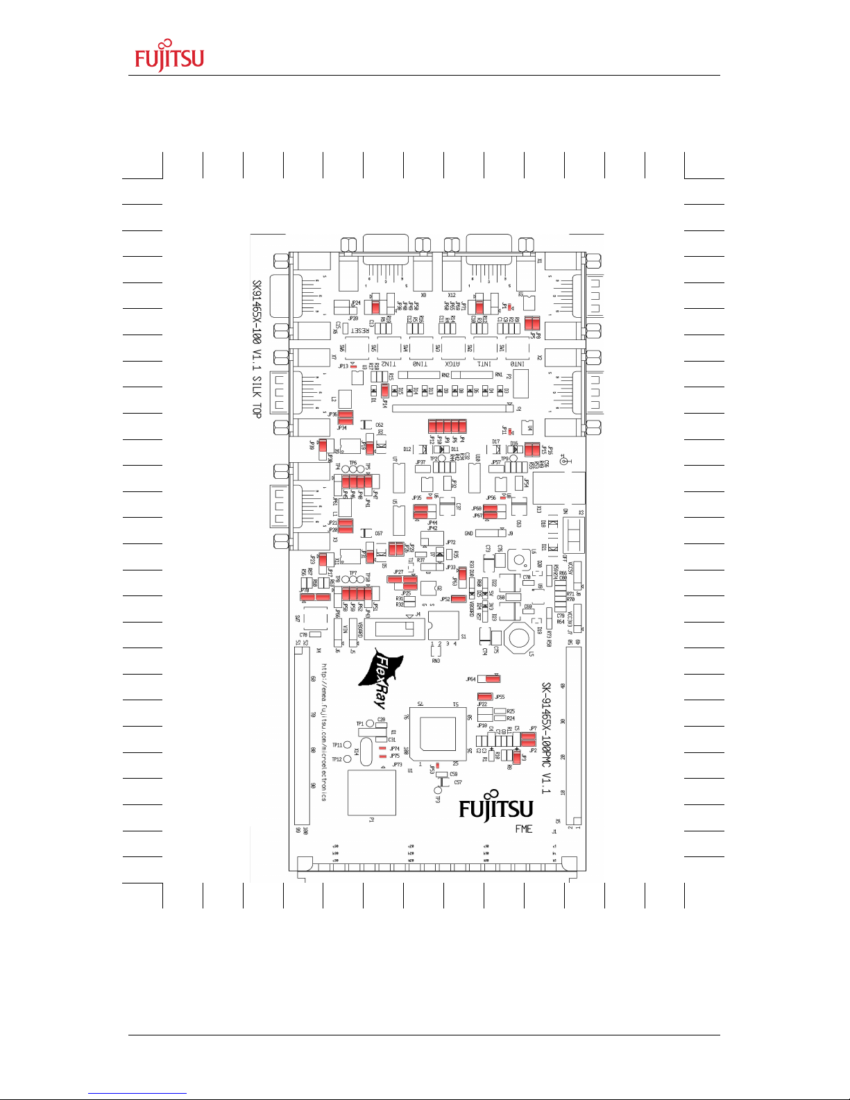
6 Silk-Plot of the Board
6.1 Silk-plot Top-side
© Fujitsu Microelectronics Europe GmbH - 33 - UG-910056-11
Figure 6-1: Silk-plot top side
Page 34

6.2 Silk-plot bottom side
SK-91465X-100PMC User Guide
Chapter 6 Silk-Plot of the Board
UG-910056-11 - 34 - © Fujitsu Microelectronics Europe GmbH
Figure 6-2: Silk-plot Bottom side
Page 35

SK-91465X-100PMC User Guide
Chapter 7 Related Products
7 Related Products
< SK-91465X-100PMC Evaluation board for the MB91F465X MCU
in FPT-100P-M20 package
< MB2198-01 Emulator debugger main unit
< MB2198-10 DSU cable
< EMA-MB91V460A-00x Emulation Pod including MB91V460A
< EMA-MB91V460A-100 FlexRay extension board
< EMA-MB91465X-NLS-100M20 Emulator probe cable for MB91F465X MCU
< NQPack100SD-ND Socket for package FPT-100P-M20
(Tokyo Eletech Corp. www.tetc.co.jp/e_tet.htm)
< HQPack100SD Header for NQPACK100SD
< MB91460 Series
< MB91V460A MB91460 Series Evaluation chip
< MB91F465XAPMC Flash MCU
© Fujitsu Microelectronics Europe GmbH - 35 - UG-910056-11
Page 36

8 Appendix
8.1 Tables
SK-91465X-100PMC User Guide
Chapter 8 Appendix
Table 2-1: Default jumper settings........................................................................................11
Table 3-1: MCU operating mode..........................................................................................13
Table 3-2: Power supply jumper settings..............................................................................15
Table 3-3: Jumper Settings FlexRay power switching..........................................................15
Table 3-4: Jumper settings for Analogue Power supply........................................................16
Table 3-5: UART “A” jumper settings ...................................................................................17
Table 3-6: UART “B”/ LIN “A” jumper settings......................................................................18
Table 3-7: UART “C”/ LIN “B” jumper settings......................................................................19
Table 3-8: CAN “A” jumper settings......................................................................................19
Table 3-9: CAN “B” jumper settings......................................................................................19
Table 3-10: FlexRay “Channel A” jumper settings................................................................20
Table 3-11: FlexRay “Channel B” jumper settings................................................................21
Table 3-12: Reset Jumper Settings......................................................................................22
Table 3-13: Buttons Jumper settings................................................................................... 23
Table 5-1: MCU Pin Connectors ..........................................................................................27
Table 5-2: UART Connector Signals....................................................................................28
Table 5-3: CAN Connector Signals......................................................................................29
Table 5-4: FlexRay Connector Signals.................................................................................29
Table 5-5: In-Circuit Programming Connector......................................................................31
Table 5-6: VG96 (J1) Signals...............................................................................................32
UG-910056-11 - 36 - © Fujitsu Microelectronics Europe GmbH
Page 37

8.2 Figures
SK-91465X-100PMC User Guide
Chapter 8 Appendix
Figure 2-1: AC plug adapter...................................................................................................9
Figure 2-2: AC plug adapter selection....................................................................................9
Figure 2-3: DC voltage selection............................................................................................9
Figure 2-4: Low voltage adapter selection..............................................................................9
Figure 2-5: Jumper Coordinates...........................................................................................12
Figure 3-1: MCU Mode Switch.............................................................................................13
Figure 4-1: J4 Flash programming socket............................................................................26
Figure 5-1: Power Connector...............................................................................................27
Figure 5-2: UART Connector................................................................................................28
Figure 5-3: CAN Connector..................................................................................................29
Figure 5-4: FlexRay Connector............................................................................................29
Figure 5-5: In Circuit Programming Connector.....................................................................31
Figure 6-1: Silk-plot top side................................................................................................. 33
Figure 6-2: Silk-plot Bottom side..........................................................................................34
© Fujitsu Microelectronics Europe GmbH - 37 - UG-910056-11
Page 38

SK-91465X-100PMC User Guide
Chapter 9 China-RoHS regulation
9 China-RoHS regulation
Evaluation Board
Emulation Board
根据SJ/T11364-2006
《电子信息产品污染控制标识要求》特提供如下有关污染控制方面的信息。
The following product pollution control information is provided according to SJ/T11364-2006
Marking for Control of Pollution caused by Electronic Information Products.
1.电子信息产品污染控制标志说明 Explanation of Pollution Control Label
评估板
仿真板
该标志表明本产品含有超过中国标准SJ/T11363-2006
《电子信息产品中有毒有害物质的限量要求》中限量的有毒有害物质。标志中的数字为本产品
的环保使用期,表明本产品在正常使用的条件下,有毒有害物质不会发生外泄或突变,用户使
用本产品不会对环境造成严重污染或对其人身、财产造成严重损害的期限,单位为年。
为保证所申明的环保使用期限,应按产品手册中所规定的环境条件和方法进行正常使用,并严
格遵守产品维修手册中规定的定期维修和保养要求。
产品中的消耗件和某些零部件可能有其单独的环保使用期限标志,并且其环保使用期限有可能
比整个产品本身的环保使用期限短。应到期按产品维修程序更换那些消耗件和零部件,以保证
所申明的整个产品的环保使用期限。
本产品在使用寿命结束时不可作为普通生活垃圾处理,应被单独收集妥善处理。
请注意:环保使用期限50年的指定不是与产品的耐久力,使用期限或任何担保要求等同的。
This symbol to be added to all EIO sold to China, indicates the product contains hazardous
materials in excess of the limits established by the Chinese standard SJ/T11363-2006
Requirements for Concentration Limits for Certain Hazardous Substances in Electronic
Information Products. The number in the symbol is the Environment-friendly Use Period
(EFUP), which indicates the period, starting from the manufacturing date, during which the
toxic or hazardous substances or elements contained in electronic information products will
not leak or mutate under normal operating conditions so that the use of such electronic
information products will not result in any severe environmental pollution, any bodily injury or
damage to any assets, the unit of the period is “Year”.
UG-910056-11 - 38 - © Fujitsu Microelectronics Europe GmbH
Page 39

SK-91465X-100PMC User Guide
Chapter 9 China-RoHS regulation
In order to maintain the declared EFUP, the product shall be operated normally according to
the instructions and environmental conditions as defined in the product manual, and periodic
maintenance schedules specified in Product Maintenance Procedures shall be followed
strictly.
Consumables or certain parts may have their own label with an EFUP value less than the
product. Periodic replacement of those consumables or parts to maintain the declared EFUP
shall be done in accordance with the Product Maintenance Procedures.
This product must not be disposed of as unsorted municipal waste, and must be collected
separately and handled properly after decommissioning.
Please note: The designation of 10 years EFUP is not to be equated with the durability, useduration or any warranty-claims of the product.
产品中有毒有害物质或元素的名称及含量
Table of hazardous substances name and concentration
部件
部件
名称
名称
部件部件
名称名称
Component Name
有毒有害物质
有毒有害物质
有毒有害物质有毒有害物质
Hazardous substances name
或元素
或元素
或元素或元素
SK-91465X-100PMC
铅铅铅铅
(Pb)
x o o o o o
汞汞汞汞
(Hg)
镉镉镉镉
(Cd)
六价铬
六价铬
六价铬六价铬
(Cr(VI))
多溴联苯
多溴联苯
多溴联苯多溴联苯
(PBB)
多溴二苯醚
多溴二苯醚
多溴二苯醚多溴二苯醚
(PBDE)
O: 表示该有毒有害物质在该部件所有均质材料中的含量均在
表示该有毒有害物质在该部件所有均质材料中的含量均在SJ/T11363-2006 标准规定的限量要求以下
表示该有毒有害物质在该部件所有均质材料中的含量均在表示该有毒有害物质在该部件所有均质材料中的含量均在
X: 表示该有毒有害物质至少在该部件的某一均质材料中的含量超出
表示该有毒有害物质至少在该部件的某一均质材料中的含量超出SJ/T11363-2006 标准规定的限量要求
表示该有毒有害物质至少在该部件的某一均质材料中的含量超出表示该有毒有害物质至少在该部件的某一均质材料中的含量超出
标准规定的限量要求以下
标准规定的限量要求以下标准规定的限量要求以下
标准规定的限量要求
标准规定的限量要求标准规定的限量要求
• 此表所列数据为发布时所能获得的最佳信息
•
由于缺少经济上或技术上合理可行的替代物质或方案,此医疗设备运用以上一些有毒有害物质来实现设备的预期
临床功能,或给人员或环境提供更好的保护效果
。
O: Indicates that this toxic or hazardous substance contained in all of the homogeneous
materials for this part is below the limit requirement in SJ/T11363-2006.
X: Indicates that this toxic or hazardous substance contained in at least one of the
homogeneous materials used for this part is above the limit requirement in SJ/T11363-2006.
• Data listed in the table represents best information available at the time of publication
© Fujitsu Microelectronics Europe GmbH - 39 - UG-910056-11
Page 40

SK-91465X-100PMC User Guide
Chapter 10 Recycling
10 Recycling
Gültig für EU-Länder:
Gemäß der Europäischen WEEE-Richtlinie und deren Umsetzung in landesspezifische
Gesetze nehmen wir dieses Gerät wieder zurück.
Zur Entsorgung schicken Sie das Gerät bitte an die folgende Adresse:
Fujitsu Microelectronics Europe GmbH
Warehouse
Monzastraße 4a
63225 Langen
Valid for European Union Countries:
According to the European WEEE-Directive and its implementation into national laws we
take this device back.
For disposal please send the device to the following address:
Fujitsu Microelectronics Europe GmbH
Warehouse
Monzastraße 4a
63225 Langen
-- END --
UG-910056-11 - 40 - © Fujitsu Microelectronics Europe GmbH
 Loading...