

Page 1
Fujitsu Microelectronics Europe
User Guide
FMEMCU-UG-910074-11
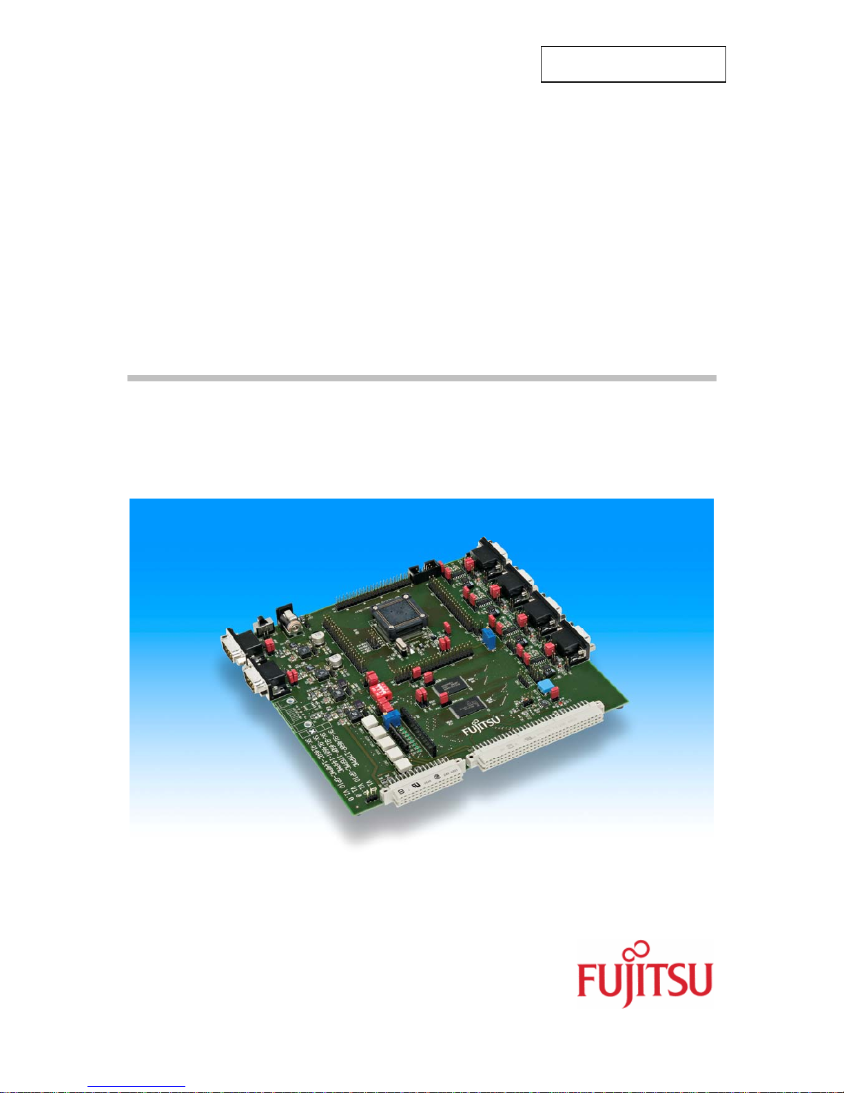
MB91460 SERIES
EVALUATION BOARD
SK-91460T-144PMC-GPIO
USER GUIDE
Page 2
SK-91460T-144PMC-GPIO User Guide
Revision History
FMEMCU-UG-910074-11 - 2 - © Fujitsu Microelectronics Europe GmbH
Revision History
Date Issue
2008/05/15 MHe - Initial version V1.0
2008/06/12 MHe - Itypos corrected V1.1
This document contains 47 pages.
Page 3

SK-91460T-144PMC-GPIO User Guide
Warranty and Disclaimer
© Fujitsu Microelectronics Europe GmbH - 3 - FMEMCU-UG-910074-11
Warranty and Disclaimer
To the maximum extent permitted by applicable law, Fujitsu Microelectronics Europe GmbH restricts
its warranties and its liability for the SK-91460T -144PMC-GPIO Board and all its deliverables (eg.
software include or header files, application examples, target boards, evaluation boards, engineering
samples of IC’s etc.), its performance and any consequential damages, on the use of the Product in
accordance with (i) the terms of the License Agreement and the Sale and Purchase Agreement under
which agreements the Product has been delivered, (ii) the technical descriptions and (iii) all
accompanying written materials. In addition, to the maximum extent permitted by applicable law,
Fujitsu Microelectronics Europe GmbH disclaims all warranties and liabilities for the performance of
the Product and any consequential damages in cases of unauthorised decompiling and/or reverse
engineering and/or disassembling. Note, the SK-91460T-144PMC-GPIO Board and all its
deliverables are intended and must only be used in an evaluation laboratory environment.
1. Fujitsu Microelectronics Europe GmbH warrants that the Product will perform substantially in
accordance with the accompanying written materials for a period of 90 days form the date of
receipt by the customer. Concerning the hardware components of the Product, Fujitsu
Microelectronics Europe GmbH warrants that the Product will be free from defects in material
and workmanship under use and service as specified in the accompanying written materials
for a duration of 1 year from the date of receipt by the customer.
2. Should a Product turn out to be defect, Fujitsu Microelectronics Europe GmbH´s entire liability
and the customer’s exclusive remedy shall be, at Fujitsu Microelectronics Europe GmbH´s
sole discretion, either return of the purchase price and the license fee, or replacement of the
Product or parts thereof, if the Product is returned to Fujitsu Microelectronics Europe GmbH in
original packing and without further defects resulting from the customer’s use or the transport.
However, this warranty is excluded if the defect has resulted from an accident not attributable
to Fujitsu Microelectronics Europe GmbH, or abuse or misapplication attributable to the
customer or any other third party not relating to Fujitsu Microelectronics Europe GmbH.
3. To the maximum extent permitted by applicable law Fujitsu Microelectronics Europe GmbH
disclaims all other warranties, whether expressed or implied, in particular, but not limited to,
warranties of merchantability and fitness for a particular purpose for which the Product is not
designated.
4. To the maximum extent permitted by applicable law, Fujitsu Microelectronics Europe GmbH´s
and its supplier’s liability are restricted to intention and gross negligence.
NO LIABILITY FOR CONSEQUENTIAL DAMAGES
To the maximum extent permitted by applicable law, in no event shall Fujitsu
Microelectronics Europe GmbH and its suppliers be liable for any damages whatsoever
(including but without limitation, consequential and/or indirect damages for personal
injury, assets of substantial value, loss of profits, interruption of business operation,
loss of information, or any other monetary or pecuniary loss) arising from the use of
the Product.
Should one of the above stipulations be or become invalid and/or unenforceable, the remaining
stipulations shall stay in full effect
Page 4

SK-91460T-144PMC-GPIO User Guide
Contents
FMEMCU-UG-910074-11 - 4 - © Fujitsu Microelectronics Europe GmbH
0 Contents
REVISION HISTORY............................................................................................................2
WARRANTY AND DISCLAIMER.........................................................................................3
0 CONTENTS......................................................................................................................4
1 OVERVIEW...................................................................................................................... 6
1.1 Abstract................................................................................................................... 6
1.2 Features.................................................................................................................. 6
1.3 General Description................................................................................................. 7
2 INSTALLATION............................................................................................................... 9
2.1 Connection/Power-On............................................................................................. 9
2.2 Default Jumper settings for SK-MB91460T-144PMC-GPIO................................... 10
2.3 Jumper Location.................................................................................................... 12
2.4 Software Installation.............................................................................................. 13
3 JUMPERS AND SWITCHES..........................................................................................14
3.1 Operating Mode (S1)............................................................................................. 14
3.2 Power Supply (S3, JP: 8, 9, 11, 12, 66)................................................................. 15
3.3 Analog Power Supply Voltage (JP: 3, 5, 7)............................................................ 17
3.4 LIN / UART Connectors (X2 – X5)......................................................................... 18
3.5 CAN interfaces (X7-X8)......................................................................................... 22
3.6 Reset Generation (JP: 13, 15, 16, 18, 29, 32, 38, 42, 43)..................................... 22
3.7 User Buttons SW1, SW2, SW3, SW4, SW5 (JP: 1, 2, 4, 6, 14) ............................. 24
3.8 User potentiometer (RP2, JP41)............................................................................ 24
4 CONNECTORS..............................................................................................................25
4.1 Power connector (X6)............................................................................................ 25
4.2 Edge connector (J1, J2, J3, J4)............................................................................. 25
4.3 LIN-UART connectors (X2-X5) .............................................................................. 26
4.4 CAN Connector (X7-X8)........................................................................................ 26
4.5 USER-LEDs & optional LC-Display ....................................................................... 27
4.6 In-Circuit-Programming Connector (X1) ................................................................ 28
5 GETTING STARTED......................................................................................................29
5.1 Introduction to Softune Workbench ....................................................................... 29
5.2 Project Start-up ..................................................................................................... 31
5.1 Softune Workbench Debugger ............................................................................. 33
Page 5

SK-91460T-144PMC-GPIO User Guide
Contents
© Fujitsu Microelectronics Europe GmbH - 5 - FMEMCU-UG-910074-11
6 PROGRAMMING THE INTERNAL FLASH.................................................................... 35
6.1 Asynchronous Mode.............................................................................................. 35
6.2 Synchronous Mode ............................................................................................... 38
7 TROUBLESHOOTING................................................................................................... 39
8 APPENDIX..................................................................................................................... 40
8.1 Related Products................................................................................................... 40
8.2 Information in the WWW........................................................................................ 41
8.3 Tables ................................................................................................................... 42
8.4 Figures.................................................................................................................. 43
8.5 Abbreviations ........................................................................................................ 44
9 CHINA-ROHS REGULATION........................................................................................45
10 RECYCLING..................................................................................................................47
Page 6

SK-91460T-144PMC-GPIO User Guide
Chapter 1 Overview
FMEMCU-UG-910074-11 - 6 - © Fujitsu Microelectronics Europe GmbH
1 Overview
1.1 Abstract
The SK-91460T-144PMC-GPIO is a multifunctional evaluation board for the Fujitsu 32-bit
FR60 Flash microcontroller series MB91460.
It can be used stand-alone for software development and testing or as a simple target board
to work with the emulator system.
The board allows the designer immediately to start software development before his own
final target system is available.
1.2 Features
< Supports Fujitsu’s MB91F467TA MCU in FPT-144P-M08 package or the MB2198
Emulator System (ICE 2198-01 + EMA-MB91V460A-002B-80) with the Probe Cables
EMA-MB91F467T-NLS-144M08 or EMA-MB91F467T-LS-144M08.
< 9-15V unregulated external DC power supply
< 5V and 3.3V onboard switching mode voltage regulators
< Power-LEDs for all supply voltages
< Onboard voltage supervisor monitors both supply voltages
< In-Circuit serial Flash programming (UART4)
< All resources available for evaluation
< All MCU pins routed to connectors
< 4 MHz main crystal
< 32 kHz crystal for sub clock operation
< Four RS232- or LIN interfaces and two CAN interfaces are usable simultaneously
< 3V capable CAN, LIN and RS232 transceivers
< 8 User LEDs, optional: alphanumeric standard LC-Display connectable instead of LEDs
< Reset button, Reset LED
< 5 User buttons
< 10-turn potentiometer connectable to ADC channel.
This board must only be used for test applications
in an evaluation laboratory environment.
Page 7

SK-91460T-144PMC-GPIO User Guide
Chapter 1 Overview
© Fujitsu Microelectronics Europe GmbH - 7 - FMEMCU-UG-910074-11
1.3 General Description
The SK-91460T-144PMC-GPIO supports the 32-bit Flash microcontroller MB91F467TA.
It can be used as a stand-alone evaluation board or as a target board for the emulator
debugger.
The evaluation board supports the following package: FPT-144P-M08.
1.3.1 MCU Clocks
The board is supplied with a 4 MHz crystal as main oscillation source. Using the internal PLL
of the µC, internal clock rates up to 100 MHz can be achieved.
1.3.2 RS-232 and LIN
Four separate RS232 transceivers and four single-wire LIN-transceivers (TLE7259) are
available to connect four on-chip UARTs to 9-pin D-Sub connectors (X2-X5). The
transceivers generate the adequate RS232 levels for the receive (RXD) and transmit (TXD)
and LIN bus lines. In RS232 mode, either the DTR line or the RTS line can be selected with
jumpers (JP24, 50, 51, 89) to generate a system reset. The RTS signal can be shortcut to
CTS using the jumpers JP17, 20, 44 and 45. Each of the four D-Sub connectors can be
configured as RS232 or LIN. The LIN Vs line can be powered by the unregulated supply
input of the board, so no additional supply is needed (JP30, 31, 56 and 57).
All transceivers are fully 3.3V IO compatible to enable low voltage applications.
In-circuit programming (asynchronous) can be done via LIN-UART 4 (X2).
1.3.3 CAN Bus
Two high-speed CAN transceivers (TLE6250GV33) can be connected to the CAN interfaces
of the MCU to allow easy connection to CAN networks.
All transceivers are fully 3.3V IO compatible to enable low voltage applications.
1.3.4 MCU Pins / External Bus Interface Connector
All pins of the microcontroller except the oscillator pins X0/1(A) are connected to edge
connectors in functional groups and are directly available to the user.
1.3.5 Power Supply
The on-board switching mode voltage regulators allow the user to connect an unregulated
DC input voltage of +9V to +15V, and supplies all voltages needed by the board. The
regulators are rated with 3A (5V and 3.3V) and are thermally protected against overload.
1.3.6 User Buttons
There are six push button switches on the board, which can be connected to input ports of
the microcontroller. This allows the user to evaluate external Interrupts, external ADC trigger
or Input Capture functions as well as simple input polling. One button is reserved as ‘Reset’button for the microcontroller, controlled by the supply monitor IC.
1.3.7 User LEDs and optional LCD
Eight user LEDs are connected to Port 15/16 and grounded by a 1k resistor network. If these
LEDs are not required, the resistor network can be removed to disconnect the LEDs and to
free the IO port.
Page 8
SK-91460T-144PMC-GPIO User Guide
Chapter 1 Overview
FMEMCU-UG-910074-11 - 8 - © Fujitsu Microelectronics Europe GmbH
1.3.8 I2C Bus
Additional pull-up resistors can be connected to the I²C bus lines by setting the according
Jumpers (JP68, 76, 90, 92) for I²C 0/1.
1.3.9 Emulator System
If the board is used as an emulator target board, the microcontroller must be removed from
the socket and the corresponding probe cable has to be mounted:
Table 1-1: Emulation System
Attention:
Socket for Flash chip mounting and probe cable connection is very sensitive. Always fit
probe cable or socket cover very carefully. If any unexpected problems occur, please check
proper connection of MCU/probe cable pads to socket.
Note:
Some customers experience connectivity problems when connecting the MCU into
the socket adapter. Only the small red screwdriver available in your box should be
used to connect the cover (HQPACK) onto the socket (NQPACK).
If the four screws are not tightening equally, then it may cause a poor contact.
Do not screw the cover too tight (max 0.054 Nm). If you have connectivity problems
then please loosen the screws and tighten again the screws equally.
Do not clean NQPACK, YQPACK, and YQSOCKET with steam. Cleaning material will
contaminate inside of connector.
Series V-Chip Probe cable Socket
MB91460 EMA-MB91V460A-002B-80
EMA-MB91F467T-NLS-144M08
EMA-MB91F467T-LS-144M08
NQPACK144SD-ND
HQPACK144SD
Page 9

SK-91460T-144PMC-GPIO User Guide
Chapter 2 Installation
© Fujitsu Microelectronics Europe GmbH - 9 - FMEMCU-UG-910074-11
2 Installation
2.1 Connection/Power-On
Carefully remove the board from the shipping carton.
First, check if there are any damages before powering up the evaluation board.
For the power supply a DC input voltage of 9V – 15V is recommended. The positive
voltage (+) must be connected to the center pin, and ground (GND) must be
connected to the shield of the connector X6!
Special care must be taken to the max. input voltage, if the LIN Vs lines are supplied
by the board (JP30, 31, 56, 57), since the input supply voltage is directly applied to pin
1 of X2-X5 without a voltage regulator.
After power-on (Switch S3 or JP66), the yellow power-on LEDs (D20 and D28) should be lit.
If the LEDs do not light up, switch off the power supply and check input polarity and current
capability of the DC supply used.
To use the MCU with the internal flash, which is normally required for the final application,
the CPU mode selection must be set to the Internal Reset Vector mode by setting DIP switch
S1 to (Off, Off, Off, Off)
The in-circuit programming allows the user to program own applications into the Flash
memory. The procedures for Flash programming are described in chapter 6.
If the board shall be used as an emulator target board, switch off the power supply and
remove the microcontroller from the socket. Now the probe cable can be mounted on the
socket. Take care of the pin 1 marking on the socket and fasten the probe cable with the
provided screws.
Do not use any other probe cable than EMA-MB91F467T-NLS-144M08 or
EMA-MB91F467T-LS-144M0
Connect the probe cable to the EMA-MB91V460A-002B-80 Adapter Board. Check all jumper
settings of the evaluation board, the Probe Cable and the Adapter Board.
When turning on the system, be sure to use the following power-up sequence:
1. Power up the Emulator Main Unit (MB2198-01)
2. Power up the Adapter Board (EMA-MB91V460A-002B-80)
3. Power up the target Board (SK-91460T-144PMC-GPIO)
To turn off the system, switch off the components in reverse order, beginning with the target
board.
Please refer to the corresponding user manuals and application notes for the emulator how
to set up the emulator system. After power on, the ‘Reset’-LED of the emulator must be off
and the ‘Vcc’-LED must be on.
If the Reset LED is still lit, check the settings of the emulator system and the power supply of
the evaluation board.
Page 10

SK-91460T-144PMC-GPIO User Guide
Chapter 2 Installation
FMEMCU-UG-910074-11 - 10 - © Fujitsu Microelectronics Europe GmbH
2.2 Default Jumper settings for SK-MB91460T-144PMC-GPIO
The following table lists all jumpers including its default setting and location on the starterkit.
Jumper Description / Function Type
Default
Setting
Coordinates
JP1 SW1 (INT0) Jumper 3 pin 1-2 E 12
JP2 SW2 (INT1) Jumper 3 pin 1-2 E 12
JP3 AVcc Jumper 2 pin Closed H 9
JP4 SW3 (ATGX) Jumper 2 pin Closed E 12
JP5 AVCC=AVRH Jumper 2 pin Closed J 7
JP6 SW4 (ICU0/TIN0) Jumper 2 pin Closed E 12
JP7 AVss Jumper 2 pin Closed H 9
JP8 VDD35 Solder JP 3 pin 1-2 E 8
JP9 VDD5 Jumper 2 pin Closed E 9
JP11 VDD5 Jumper 3 pin 1-2 E 9
JP12 VDD5R Jumper 3 pin 1-2 E 9
JP13 DTR / DTRx Jumper 3 pin Open K 15
JP14 SW5 (NMIX) Jumper 2 pin Closed E 12
JP15 Reset by UART5 Jumper 2 pin Open L 13
JP16 Reset by UART4 Jumper 2 pin Open L 13
JP17 RTS-CTS UART5 Jumper 2 pin Closed M 6
JP18 Reset: immediate / delayed Solder JP 3 pin 1-2 K 15
JP20 UART0/4: RTS-CTS Jumper 2 pin Closed M 2
JP21 SIN4: RS232 / LIN Jumper 3 pin 1-2 L 2
JP22 SIN5: RS232 / LIN Jumper 3 pin 1-2 L 5
JP24 UART5: DTR/RTS Jumper 3 pin Open M 5
JP25 SOT4: RS232 / LIN Jumper 3 pin 1-2 L 2
JP26 SOT5: RS232 / LIN Jumper 3 pin 1-2 L 6
JP27 LIN-UART 4: RS232 / LIN Jumper 3 pin 1-2 M 2
JP28 LIN-UART 5: RS232 / LIN Jumper 3 pin 1-2 M 6
JP29 Monitor 2.5V/1.8V Solder JP 3 pin 2-3 J 16
JP30 LIN4: VBat Jumper 2 pin Open M 2
JP31 LIN5: VBat Jumper 2 pin Open M 5
JP32 Monitor 2V5 / 3V3 Solder JP 3 pin 2-3 J16
JP33 LIN4: Enable Jumper 2 pin Open M 3
JP35 LIN5: Enable Jumper 2 pin Open M 6
JP36 Mounting option: TLE7259/TLE6259 Solder JP 3 pin 1-2 L 3
JP37 Mounting option: TLE7259/TLE6259 Solder JP 3 pin 1-2 L 7
JP38 Reset MCU Jumper 2 pin Closed L 16
JP39 LIN 4: Master Jumper 2 pin Open M 4
JP40 LIN 5: Master Jumper 2 pin Open M 7
JP41 ADC Jumper 2 pin Open K 8
JP42 Reset by UART6 Jumper 2 pin Open L 14
JP43 Reset by UART7 Jumper 2 pin Open L 14
JP44 UART6: RTS-CTS Jumper 2 pin Closed M 9
JP45 UART7: RTS-CTS Jumper 2 pin Closed M 12
JP48 SIN6: RS232 / LIN Jumper 3 pin 1-2 L 8
Page 11
SK-91460T-144PMC-GPIO User Guide
Chapter 2 Installation
© Fujitsu Microelectronics Europe GmbH - 11 - FMEMCU-UG-910074-11
Jumper Description / Function Type
Default
Setting
Coordinates
JP49 SIN7: RS232 / LIN Jumper 3 pin 1-2 L 12
JP50 UART6: DTR/RTS Jumper 3 pin Open M 9
JP51 UART7: DTR/RTS Jumper 3 pin Open M 12
JP52 SOT6: RS232 / LIN Jumper 3 pin 1-2 L 9
JP53 SOT7: RS232 / LIN Jumper 3 pin 1-2 L 12
JP54 LIN-UART 6: RS232 / LIN Jumper 3 pin 1-2 M 9
JP55 LIN-UART 7: RS232 / LIN Jumper 3 pin 1-2 M 12
JP56 LIN 6: VBat Jumper 2 pin Open M 8
JP57 LIN 7: VBat Jumper 2 pin Open M 12
JP59 LIN6: Enable Jumper 2 pin Open M 10
JP61 LIN7: Enable Jumper 2 pin Open M 13
JP62 Mounting option: TLE7259/TLE6259 Solder JP 3 pin 1-2 M 10
JP63 Mounting option: TLE7259/TLE6259 Solder JP 3 pin 1-2 M 13
JP64 LIN6: Master Jumper 2 pin Open M 11
JP65 LIN7: Master Jumper 2 pin Open M 14
JP66 MAINS Jumper 2 pin Open C 2
JP66A
Mounting option:
TLE6250GV33/PCA82C250E6250GV33/
PCA82C250
Solder JP 3 pin 1-2 C 2
JP66B
Mounting option:
TLE6250GV33/PCA82C250TLE6250GV33/
PCA82C250
Solder JP 3 pin 1-2 C 5
JP68 SDA0 Pullup Jumper 2 pin Open F 5
JP69 CAN0 RX Jumper 2 pin Closed B 3
JP70 CAN1 RX Jumper 2 pin Closed B 7
JP72 CAN0 TX Jumper 2 pin Closed B 3
JP73 CAN1 TX Jumper 2 pin Closed B 7
JP76 SCL0 Pullup Jumper 2 pin Open F 6
JP89 UART4: DTR/RTS Jumper 3 pin Open M 2
JP90 SDA1 Pullup Jumper 2 pin Open F 6
JP92 SCL1 Pullup Jumper 2 pin Open F 6
JP104 MD3, fast clock input Jumper 3 pin 1-2 F10
Table 2-1: Jumper Settings
Page 12
SK-91460T-144PMC-GPIO User Guide
Chapter 2 Installation
FMEMCU-UG-910074-11 - 12 - © Fujitsu Microelectronics Europe GmbH
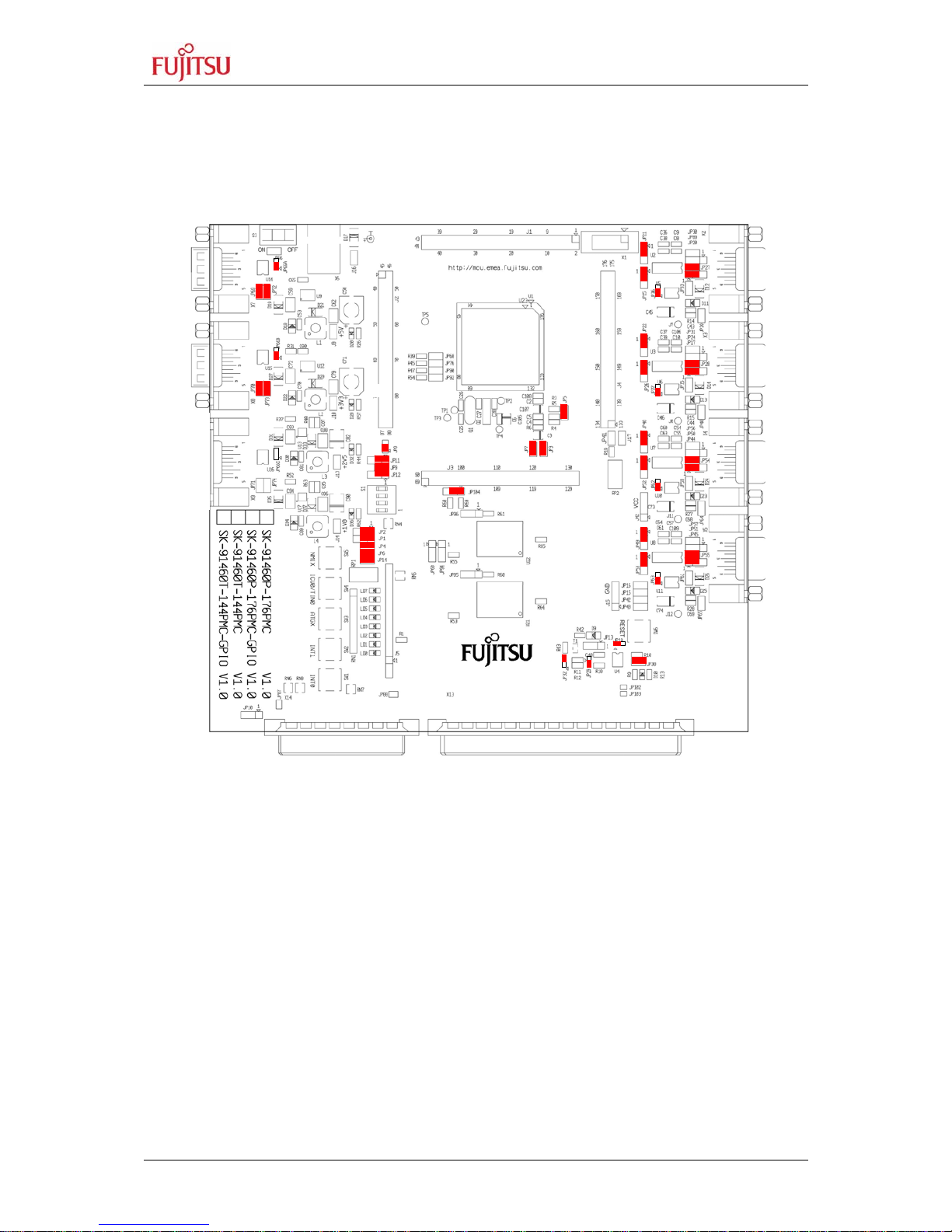
2.3 Jumper Location
The following picture shows the silk plot of the starter-kit with marked default jumper
settings.
A B C D E F G H J K L M N
1 1
2 2
3 3
4 4
5
5
6 6
7 7
8 8
9 9
10 10
11 11
12 12
13 13
14 14
15 15
16 16
17 17
18 18
19
19
A B C D E F G H J K L M N
Figure 2-1: Default Jumper Settings
LIN-UART 5 LIN-UART 6 LIN-UART 7 LIN-UART 4
CAN 0 CAN 1
X
Page 13
SK-91460T-144PMC-GPIO User Guide
Chapter 2 Installation
© Fujitsu Microelectronics Europe GmbH - 13 - FMEMCU-UG-910074-11
2.4 Software Installation
2.4.1 Installation of Softune Workbench
With the “SK-91460T-144PMC-GPIO” Fujitsu supplies a full working development
environment called Softune Workbench V6. To develop own software the Softune
Workbench development environment must be installed first. Follow the instructions for
successful installation of the Softune Workbench.
1) Before starting the installation setup ensure that you are logged in with administrator
or poweruser permissions, otherwise the Softune Workbench installation will fail! Be
aware that Softune Workbench does not support multi-user support. Therefore
install- and user login must be the same.
2) Browse on the Micros DVD-ROM to “Software Registration”. After your free online
registration you will receive your password by email.
3) Browse on the Micros DVD-ROM to “Software and Utilities” for installation Softune
Workbench.
4) Follow the installation instructions.
5) For the default installation path it is recommended to use c:\Softune6.
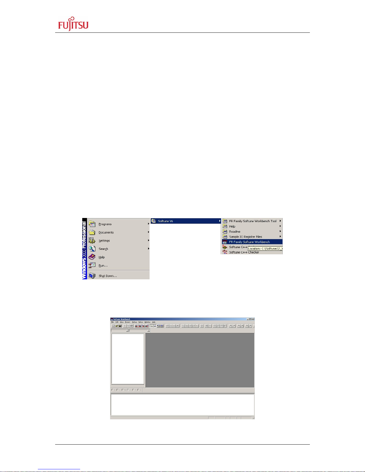
6) After the installation is finished. The FR Family Softune Workbench can be started
via the Windows “Start” menu.
Figure 2-2: Softune Workbench Start Menu Location
7) When Softune Workbench was started the following window will be shown.
Figure 2-3: Softune Workbench V6 IDE
Page 14
SK-91460T-144PMC-GPIO User Guide
Chapter 3 Jumpers and Switches
FMEMCU-UG-910074-11 - 14 - © Fujitsu Microelectronics Europe GmbH
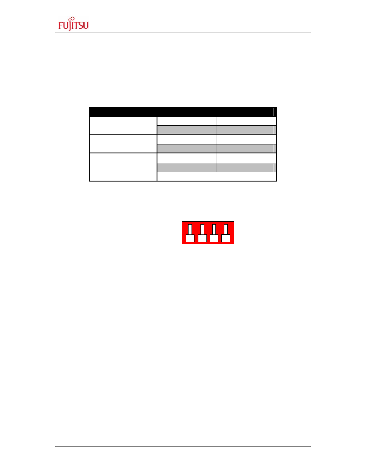
ON
OFF
DIP-Switch S1
(default setting)
1
2 3 4
MD0 MD1 MD2 NC
3 Jumpers and Switches
This chapter describes all jumpers and switches that can be modified on the evaluation
board. The default setting is shown with a grey shaded area.
3.1 Operating Mode (S1)
DIP switch Setting Logical value
ON (closed) 1 (high)
S1/1 (MD0)
OFF (open) 0 (low)
ON (closed) 1 (high)
S1/2 (MD1)
OFF (open) 0 (low)
ON (closed) 1 (high)
S1/3 (MD2)
OFF (open) 0 (low)
S1/4 NC
Table 3-1: MCU Operating Mode
Figure 3-1: MCU mode switch
Page 15
SK-91460T-144PMC-GPIO User Guide
Chapter 3 Jumpers and Switches
© Fujitsu Microelectronics Europe GmbH - 15 - FMEMCU-UG-910074-11
3.2 Power Supply (S3, JP: 8, 9, 11, 12, 66)
The onboard voltage regulators provide stabilized 5V and 3.3V supplies to the MCU and
peripherals. Even though they are thermally protected against overload, care must be taken
when supplying current for additional circuitry.
The LIN Vs line can be connected directly to the input supply of the board by Jumpers. In
this case, the input voltage to the board has to be suitable for the connected bus devices
(mostly around 12V). Since there is a protection diode between Vin and Vs, it is not possible
to power the board over the LIN bus.
S3 Power Switch
JP8 Selects the MCU External Bus voltage VDD35 (3.3V or 5V)
JP9 Connects the MCU IO voltage to Vcc. Can be used for current measurement.
JP11 Selects the MCU IO and peripherals Vcc voltage (3.3V or 5V)
JP12 Selects the MCU core voltage regulator input voltage (3.3V or 5V)
JP66 Mains jumper; overrides the power switch S3.
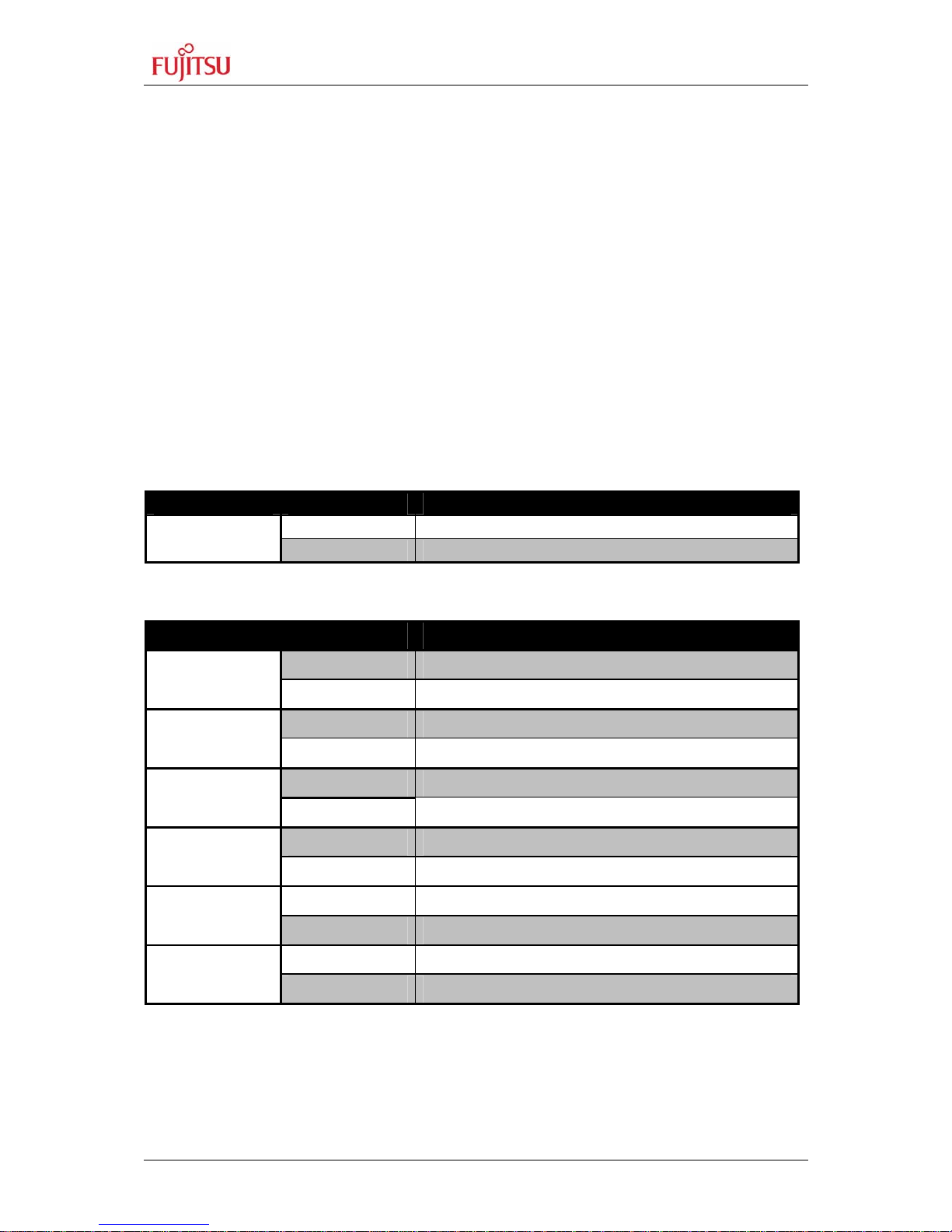
Switch Setting Description
ON (1-2) Power ON
S3
OFF (2-3) Power OFF
Table 3-2: Power Switch
Jumper Setting Description
1 - 2 External Bus @ 5V JP8
(VDD35 3V/5V)
2 - 3 External Bus @ 3.3V
Closed Power supply Vcc connected to VDD5 JP9
(VDD5)
Open Power supply Vcc not connected to VDD5
1 - 2 MCU IO / Peripherals @ 5V JP11
(VDD5 3V/5V)
2 - 3 MCU IO / Peripherals @ 3.3V
1 - 2 Supply to MCU Core voltage regulator is 5V JP12
(VDD5R)
2 - 3 Supply to MCU Core voltage regulator is 3.3V
Closed Vs (Pin1) of LIN connector is powered by the board JP30, 31, 56, 57
(VBAT)
Open No voltage supply to Vs of LIN A
Closed Board is always on JP66
(Mains)
Open S3 switches the Board on and off
Table 3-3: Power Supply Configuration
By default, I/O supply and MCU Core are set to 5V and the external bus I/F is set to 3.3 V.
Page 16

SK-91460T-144PMC-GPIO User Guide
Chapter 3 Jumpers and Switches
FMEMCU-UG-910074-11 - 16 - © Fujitsu Microelectronics Europe GmbH
Figure 3-2: Voltage Test Pins
Regulator Test Pin Voltage
U9 J9 5.0 V
U12 J10 3.3 V
- J15 GND
Table 3-4: Voltage Test Pins
X
5 V
3V3
GND
Page 17

SK-91460T-144PMC-GPIO User Guide
Chapter 3 Jumpers and Switches
© Fujitsu Microelectronics Europe GmbH - 17 - FMEMCU-UG-910074-11
3.3 Analog Power Supply Voltage (JP: 3, 5, 7)
The power supply as well as the positive reference voltage for the A/D-converter can be
provided internally or externally.
JP3, JP7 connects analog power supply voltages (AVcc and AVss)
JP5 connects the analog reference voltage AVRH to AVcc
Jumper Setting Description
Closed AVcc is connected to Vcc
JP3 (AVcc)
Open AVcc is disconnected from Vcc
Closed AVRH is connected to AVcc
JP5 (AVRH)
Open AVRH defined by resistor network
*1
Closed AVss is connected to GND
JP7 (AVss)
Open AVss is disconnected from GND
*1
By default the resistor network (R4, R6) is not mounted on the board
Table 3-5: ADC Supply
Default: JP3, JP5 and JP7 are closed
By default, the A/D-converter supply and reference voltage is same as the microcontroller
supply voltage.
Note:
If JP3 and JP7 are open, the user has to supply an adequate analog voltage supply (AVcc
and AVss) to the A/D-converter.
If JP5 is open, the resistors R4 and R6 define AVRH.
By default the resistor network (R4, R6) is not mounted on the board.
Page 18

SK-91460T-144PMC-GPIO User Guide
Chapter 3 Jumpers and Switches
FMEMCU-UG-910074-11 - 18 - © Fujitsu Microelectronics Europe GmbH
3.4 LIN / UART Connectors (X2 – X5)
There are four identical circuit blocks for LIN or RS232 connections. Each of the four D-Sub
connectors can be configured as LIN or RS232 interface. DTS or RTS can be selected as
reset source, and RTS and CTS can be connected by a jumper, since some terminals and
Flash programming tools need this connection. Pin 1 (PIN Vs) of X2-X5 can be connected to
the voltage input of the board by jumpers in order to supply the LIN bus. When using this
feature, pay attention to the input voltage of the board, since there is only a protection diode
between Vin and Vs.
LIN-UART 4:
Jumper Setting Description
1-2 SIN4 is connected to RS232 transceiver
JP21
(RXD)
2-3 SIN4 is connected to LIN transceiver
1-2 SOT4 is connected to RS232 transceiver
JP25
(TXD)
2-3 SOT4 is connected to LIN transceiver
1-2 X2 Pin2 is connected to RS232 transceiver (T1out) JP27
(RS232/LIN)
2-3 X2 Pin2 is connected to LIN transceiver (BUS)
Closed RTS and CTS of X2 are connected JP20
(RTS-CTS)
Open RTS and CTS of X2 are not connected
1-2 DTR signal (Pin 6 of X2) is used as reset source JP89
(DTR/RTS)
2-3 RTS signal (Pin 7 of X2) is used as reset source
Closed LIN transceiver for X2 is enabled JP33
(LIN enable)
Open LIN transceiver for X2 is disabled
Closed LIN-UART 4 is LIN Master JP39
(LIN master)
Open LIN-UART 4 is LIN Slave
Closed Pin 1 (LIN Vs) of X2 is connected to Vin JP30
(LIN Vbat)
Open Pin 1 (LIN Vs) of X2 is not connected to Vin
Table 3-6: UART 4 Settings
By default, UART4 is connected to X2 and configured as RS232 interface.
For Flash programming, UART4 has to be used (RS232).
Page 19

SK-91460T-144PMC-GPIO User Guide
Chapter 3 Jumpers and Switches
© Fujitsu Microelectronics Europe GmbH - 19 - FMEMCU-UG-910074-11
LIN-UART 5:
Jumper Setting Description
1-2 SIN5 is connected to RS232 transceiver
JP22
(RXD)
2-3 SIN5 is connected to LIN transceiver
1-2 SOT5 is connected to RS232 transceiver
JP26
(TXD)
2-3 SOT5 is connected to LIN transceiver
1-2 X3 Pin2 is connected to RS232 transceiver (T1out) JP28
(RS232/LIN)
2-3 X3 Pin2 is connected to LIN transceiver (BUS)
Closed RTS and CTS of X3 are connected JP17
(RTS-CTS)
Open RTS and CTS of X3 are not connected
1-2 DTR signal (Pin 6 of X3) is used as reset source JP24
(DTR/RTS)
2-3 RTS signal (Pin 7 of X3) is used as reset source
Closed LIN transceiver for X3 is enabled JP35
(LIN enable)
Open LIN transceiver for X3 is disabled
Closed LIN-UART 5 is LIN Master JP40
(LIN master)
Open LIN-UART 5 is LIN Slave
Closed Pin 1 (LIN Vs) of X3 is connected to Vin JP31
(LIN Vbat)
Open Pin 1 (LIN Vs) of X3 is not connected to Vin
Table 3-7: UART 5 Settings
By default, UART5 is connected to X3 and configured as RS232 interface.
Page 20
SK-91460T-144PMC-GPIO User Guide
Chapter 3 Jumpers and Switches
FMEMCU-UG-910074-11 - 20 - © Fujitsu Microelectronics Europe GmbH
LIN-UART 6:
Jumper Setting Description
1-2 SIN6 is connected to RS232 transceiver
JP48
(RXD)
2-3 SIN6 is connected to LIN transceiver
1-2 SOT6 is connected to RS232 transceiver
JP52
(TXD)
2-3 SOT6 is connected to LIN transceiver
1-2 X4 Pin2 is connected to RS232 transceiver (T1out) JP54
(RS232/LIN)
2-3 X4 Pin2 is connected to LIN transceiver (BUS)
Closed RTS and CTS of X4 are connected JP44
(RTS-CTS)
Open RTS and CTS of X4 are not connected
1-2 DTR signal (Pin 6 of X4) is used as reset source JP50
(DTR/RTS)
2-3 RTS signal (Pin 7 of X4) is used as reset source
Closed LIN transceiver for X4 is enabled JP59
(LIN enable)
Open LIN transceiver for X4 is disabled
Closed LIN-UART 6 is LIN Master JP64
(LIN master)
Open LIN-UART 6 is LIN Slave
Closed Pin 1 (LIN Vs) of X4 is connected to Vin JP56
(LIN Vbat)
Open Pin 1 (LIN Vs) of X4 is not connected to Vin
Table 3-8: UART 6 Settings
By default, UART6 is connected to X4 and configured as RS232 interface.
Page 21

SK-91460T-144PMC-GPIO User Guide
Chapter 3 Jumpers and Switches
© Fujitsu Microelectronics Europe GmbH - 21 - FMEMCU-UG-910074-11
LIN-UART 7:
Jumper Setting Description
1-2 SIN7 is connected to RS232 transceiver
JP49
(RXD)
2-3 SIN7 is connected to LIN transceiver
1-2 SOT7 is connected to RS232 transceiver
JP53
(TXD)
2-3 SOT7 is connected to LIN transceiver
1-2 X5 Pin2 is connected to RS232 transceiver (T1out) JP55
(RS232/LIN)
2-3 X5 Pin2 is connected to LIN transceiver (BUS)
Closed RTS and CTS of X5 are connected JP45
(RTS-CTS)
Open RTS and CTS of X5 are not connected
1-2 DTR signal (Pin 6 of X5) is used as reset source JP51
(DTR/RTS)
2-3 RTS signal (Pin 7 of X5) is used as reset source
Closed LIN transceiver for X5 is enabled JP61
(LIN enable)
Open LIN transceiver for X5 is disabled
Closed LIN-UART 7 is LIN Master JP65
(LIN master)
Open LIN-UART 7 is LIN Slave
Closed Pin 1 (LIN Vs) of X5 is connected to Vin JP57
(LIN Vbat)
Open Pin 1 (LIN Vs) of X5 is not connected to Vin
Table 3-9: UART 7 Settings
By default, UART7 is connected to X5 and configured as RS232 interface.
Page 22

SK-91460T-144PMC-GPIO User Guide
Chapter 3 Jumpers and Switches
FMEMCU-UG-910074-11 - 22 - © Fujitsu Microelectronics Europe GmbH
3.5 CAN interfaces (X7-X8)
Two high-speed CAN-transceivers can be connected to the microcontroller’s CAN interfaces
(CAN0-CAN1).
Jumper Setting Description
JP69 (CAN0 RX)
Closed RX0 of MCU is connected to CAN0 (X7)
JP72 (CAN0 TX)
Closed TX0 of MCU is connected to CAN0 (X7)
JP70 (CAN1 RX)
Closed RX1 of MCU is connected to CAN1 (X8)
JP73 (CAN1 TX)
Closed TX1 of MCU is connected to CAN1 (X8)
Table 3-10: CAN Settings
By default, twol CAN Interfaces are connected to X7-X8.
3.6 Reset Generation (JP: 13, 15, 16, 18, 29, 32, 38, 42, 43)
In addition to the internal Power-On reset, the microcontroller can be reset by an external
reset circuit (Voltage Monitor) and also by a RS232 interface. Refer to the chapter ‘LIN /
UART Connectors (X2 – X5)’ for DTR / RTS selection.
JP15, 16, 42, 43: Selects X2, X3, X4 or X5 as reset source
JP13 The signal on the DTR/RTS line can be negated with this jumper.
Remove the jumper in order to disable the RS232 reset circuit.
JP18 This solder jumper selects between normal (immediate) reset and delayed reset.
In delayed reset mode, the reset button has to be held down for 2 sec before a
reset is generated to avoid accidental resets.
JP29 This solder jumper selects the third voltage monitored by the reset IC (5V and
3.3V are always monitored).
JP32 This solder jumper selects the third voltage monitored by the reset IC (5V and
3.3V are always monitored).
JP38 Open this jumper if no external Reset shall be generated.
In this case only the internal reset is active (e.g.: power-on)
Page 23

SK-91460T-144PMC-GPIO User Guide
Chapter 3 Jumpers and Switches
© Fujitsu Microelectronics Europe GmbH - 23 - FMEMCU-UG-910074-11
Jumper Setting Description
Closed LIN-UART 4 (X2) connected to reset circuit
JP16 (RST 0/4)
Open LIN-UART 4 (X2) not connected to reset circuit
Closed LIN-UART 5 (X3) connected to reset circuit
JP15 (RST 1/5)
Open LIN-UART 5 (X3) not connected to reset circuit
Closed LIN-UART 6 (X4) connected to reset circuit
JP42 (RST 2/6)
Open LIN-UART 6 (X4) not connected to reset circuit
Closed LIN-UART 7 (X5) connected to reset circuit
JP43 (RST 3/7)
Open LIN-UART 7 (X5) not connected to reset circuit
1-2 No negation for the DTR/RTS signal
JP13 (DTR / DTRx)
2-3 DTR/RTS signal is negated
1-2 Reset is applied immediately when SW6 is pressed JP18
(Reset imm./delayed)
2-3 Reset is applied when SW6 is pressed >2sec
1-2 not allowed
JP29
2-3 VCC3V3 is monitored by reset IC
1-2 not allowed
JP32
2-3 VCC3V3 is monitored by reset IC
Closed External reset generation is active
JP38 (RST MCU)
Open No external reset generation
Table 3-11: Reset Connection
By default, the external reset is enabled and set to immediate reset, the reset by UART is
disabled.
Note:
While a reset signal is asserted the red Reset-LED D10 is lit.
During normal operation, this LED should be off!
If JP13 (DTR/DTRx) is set, one of the RST jumpers (JP15, 16, 42, 43) and the according
DTR/RTS jumper have to be set, too.
If the reset LED is steadily on, check the power supply input voltage and the settings for the
reset-generation by UART.
Page 24

SK-91460T-144PMC-GPIO User Guide
Chapter 3 Jumpers and Switches
FMEMCU-UG-910074-11 - 24 - © Fujitsu Microelectronics Europe GmbH
3.7 User Buttons SW1, SW2, SW3, SW4, SW5 (JP: 1, 2, 4, 6, 14)
JP1, 2, 4, 6, 14 Five user push buttons (SW1-SW5) can be connected to the
microcontroller.
Jumper Setting Description
1-2 Pin 118 (INT0) of the MCU is connected to “SW1”
JP1 (SW1)
2-3 Pin 28 (INT0) of the MCU is connected to “SW1”
(for PPMUX.PR0=1)
1-2 Pin 119 (INT1) of the MCU is connected to “SW2”
JP2 (SW2)
2-3 Pin 29 (INT1) of the MCU is connected to “SW2”
(for PPMUX.PR0=1)
Closed Pin 53 (ATGX) of the MCU is connected to “SW3”
JP4 (SW3)
Open No connection to the microcontroller
Closed Pin 64 (ICU0/TIN0) of the MCU is connected to “SW4”
JP6 (SW4)
Open No connection to the microcontroller
Closed Pin 85 (NMIX) of the MCU is connected to “SW5”
JP14 (SW5)
Open No connection to the microcontroller
Table 3-12: User Push Buttons
By default, all push-buttons are connected to the microcontroller.
3.8 User potentiometer (RP2, JP41)
A 10kΩ, 10-turn precision potentiometer can be connected to an ADC channel, AN6, with
the jumper JP41. The voltage to this pin can be adjusted with RP2 and measured at J17.
Jumper Setting Description
JP41 closed RP2 is connected to AN6
Table 3-13: Potentiometer Settings
Page 25

SK-91460T-144PMC-GPIO User Guide
Chapter 4 Connectors
© Fujitsu Microelectronics Europe GmbH - 25 - FMEMCU-UG-910074-11
4 Connectors
4.1 Power connector (X6)
The following figure shows the power connection jack X6. This connector is used to connect
an external unregulated DC power supply voltage (9V-15V DC) to the evaluation board.
Connector X6:
Figure 4-1: Power Connector
The switching mode voltage regulators allow a wide input range. This might be of interest
when using Vin to power the LIN bus Vs line.
4.2 Edge connector (J1, J2, J3, J4)
All pins (except oscillator Pins) of the microcontroller are directly connected to J1 to J4 as
follows:
Connector MCU Pins
J1 1 – 36
J2 37 – 72
J3 73 – 108
J4 109 – 144
The odd pin numbers are located on the one side and the even pin numbers are located on
the other side of the connector.
Shield is connected to GND
Center is connected to positive voltage supply (+)
+
Page 26

SK-91460T-144PMC-GPIO User Guide
Chapter 4 Connectors
FMEMCU-UG-910074-11 - 26 - © Fujitsu Microelectronics Europe GmbH
4.3 LIN-UART connectors (X2-X5)
Four 9-pin D-Sub female connectors are used for the serial interfaces. Note that X2 to X5
are shared between the RS232- and LIN transceivers and must be configured to the desired
functionality (refer to chapter 3.4 for details).
Figure 4-2: UART Connector
Pin Number Pin Signal Description
1 +VBat Power from / to LIN bus
TXD RS-232 transmit output
2
LIN Bi-directional LIN-interface bus
3 RXD RS-232 receive input
4 DTR Connected to DSR (pin 6)
5 GND Ground normally used for RS232 connection
6 DSR Connected to DTR (pin 4)
7 RTS Can be connected with CTS by jumper
8 CTS Can be connected with RTS by jumper
9 LGND Ground normally used for LIN connection
Shield GND Ground
Table 4-1: UART Connector Signals
4.4 CAN Connector (X7-X8)
Six 9-pin D-Sub male connectors are used for the CAN interfaces CAN0-CAN1. Both CAN
interfaces can be used simultaneously.
Figure 4-3: CAN Connector
Pin Number Pin Signal Description
1 NC Not used
2 CANL LOW-level CAN voltage input/output
3 GND Ground
4 NC Not used
5 NC Not used
6 NC Not used
7 CANH HIGH-level CAN voltage input/output
8 NC Not used
9 NC Not used
Shield GND Ground
Table 4-2: CAN Connector Signals
Page 27

SK-91460T-144PMC-GPIO User Guide
Chapter 4 Connectors
© Fujitsu Microelectronics Europe GmbH - 27 - FMEMCU-UG-910074-11
4.5 USER-LEDs & optional LC-Display
Eight LEDs are supplied for user applications. In order to disconnect the LEDs from the
related microcontroller port (Port 15, Pin 0-4 and Port 16, Pin 2-5), the resistor network RN1
can be removed.
Instead of the user-LEDs an alphanumeric LC-Display (optional) can be connected.
The potentiometer RP1 can be used to adjust the contrast of the LC-Display. Pin 15 and 16
of J1 are normally not mounted. If the used LC-Display has pins for LED backlight at this
position, they can be connected here (Pin15: Vcc via 39Ω/0.5W, Pin16: GND).
The following control signals are provided:
Figure 4-4: User LEDs/LCD
14 13 12 11 10 9 8 7 6 5 4 3 2 1 16 15
LCD
D7 D6 D5 D4 - - - - E R/W RS V0 VCC GND LED- LED+
LED
LD7 LD6 LD5 LD4 LD2 LD1 LD0
Port
16_5 16_4 16_3 16_2 15_2 15_1 15_0
Table 4-3: User LEDs/LCD
(Optional Pins: Pin15: Vcc via 39Ω/0.5W, Pin16: GND)
Pins for LCD-backlight
Page 28

SK-91460T-144PMC-GPIO User Guide
Chapter 4 Connectors
FMEMCU-UG-910074-11 - 28 - © Fujitsu Microelectronics Europe GmbH
4.6 In-Circuit-Programming Connector (X1)
There is a flash-programming socket on the starter-kit which makes it possible to program
the flash MCU with a special programming adapter. The reset signal is also available at this
connector.
Figure 4-5: In-circuit programming connector
Pin Number Pin Signal Description
1 NC Not used
2 NC Not used
3 NC Not used
4 NC Not used
5 INITX MCU reset signal
6 SIN4 UART4 receive data
7 SOT4 UART4 transmit data
8 SCK4 UART4 clock
9 VCC Board supply voltage
10 GND Ground
Table 4-4: In-circuit programming connector
Page 29

SK-91460T-144PMC-GPIO User Guide
Chapter 5 Getting Started
© Fujitsu Microelectronics Europe GmbH - 29 - FMEMCU-UG-910074-11
5 Getting Started
Make sure that the FR Family Softune Workbench is installed on your PC and the “SK91F460T-144PMC-GPIO” is ready to use (power-on, serial connection (UART4, X2) to COM
port of the PC).
5.1 Introduction to Softune Workbench
Start Softune Workbench. Select <File> <Open Workspace> to load the first example
“91460_template_91467t.wsp”. All examples can be found on our webpage at
http://mcu.emea.fujitsu.com/mcu_product/mcu_all_software.htm
.
In the project tree on the left side, you can open the “source”-folder which contains the
source-files registered to this project. A double-click on one of the files will invoke the built-in
editor, which supports syntax-highlighting, tags and various other functions.
Figure 5-1: Softune Workbench main window
Note:
You may customize the editor by a right-click on the editor
window.
Page 30

SK-91460T-144PMC-GPIO User Guide
Chapter 5 Getting Started
FMEMCU-UG-910074-11 - 30 - © Fujitsu Microelectronics Europe GmbH
Whenever you modify the source-files, you have to re-compile and link the related files to
produce a valid loadmodule (ABS-file). This is done using the MAKE-function. MAKE
invokes the assembler, C-compiler and linker for FR whenever necessary (only modified files
will be re-compiled).
If you wish to re-compile the entire project regardless of any changes, you can use the
BUILD-function. To check for syntax-errors on a specific source-file, use the
COMPILE/ASSEMBLE function.
These three functions are available on the button-bar or from the main menu (Project –
Compile / Make / Build / Abort).
Click on MAKE or BUILD. Messages from the individual language tools will be fed into the
output window at the bottom of the main screen. If the tool chain (C-compiler → Assembler
→ Linker) was completed successfully, the message “No Error” will appear.
If you get any errors during build, an appropriate message will be generated. Try this with a
simple syntax-error (e.g. delete a semicolon “;” from the end of a C-line) and click on MAKE
again. You will now see a message like this:
Now Making...
--------------------Configuration: 91460_template_91467t.prj - STANDALONE-------------------MAIN.c
*** C:\Projects\91460serie\91460_template_91467t-v10\SRC\MAIN.c(46) E4065B: expected a ";"
*** C:\Projects\91460serie\91460_template_91467t-v10\SRC\MAIN.c(57) W1012B: warning: parsing
restarts here after previous syntax error
1 error detected in the compilation of "C:\Projects\91460serie\91460_template_91467t-
v10\SRC\MAIN.c".
-----------------------------Error detected.
------------------------------
To locate the position in the source-file, where the error occurred, double-click on the
message. The editor will open the appropriate source-file, indicating the error highlighted in
red, depending on the customize settings of the editor. Correct the error and re-compile the
project as explained above.
If more errors occurred, you can go through the error list step by step using the menu “Edit –
Top/Previous/Next/Bottom Error” or using the appropriate buttons which have the same
functions:
Note:
To get on-line help about a specific error, select the error
message and press F1. In many cases, you can get some useful
hints how to solve the problem. Of course, you can also use the
HELP-menu anytime during development or debugging.
Page 31

SK-91460T-144PMC-GPIO User Guide
Chapter 5 Getting Started
© Fujitsu Microelectronics Europe GmbH - 31 - FMEMCU-UG-910074-11
5.2 Project Start-up
In order to allow a quick and smooth project start-up Fujitsu Microelectronics Europe
supplies a template project as a reference. The easiest way to start a new project is to make
a copy of the template project and use this copy as a start-up. The template includes the
latest start91460.asm file, MCU header file, IRQ table, basic linker and C-Compiler settings.
Note:
5.2.1 Create a New Project:
1. In order to start a new user-project use the “91460_template_91467t” project
2. Copy the folder 91460_template_91467t and rename the folder to e.g.
my_application
3. Enter the folder “my_application”
Rename “91460_template_91467t.prj” into “my_application.prj”
Rename “91460_template_91467t” into “my_application.wsp”
4. Edit “my_applica tio n.prj”
Rename “91460_template_91467t” -> “my_application”
5. Edit “my_applica tio n.wsp”
Rename “91460_template_91467t” -> “my_application”
In any case the settings done in the template must be checked and have to be
adjusted to the specific needs and settings of the final appli cation. The template is
providing an example for building up a new project.
THIS SAMPLE CODE IS PROVIDED AS IS AND IS SUBJECT TO ALTERATIONS. FUJITSU
MICROELECTRONICS ACCEPTS NO RESPONSIBILIT Y OR LIABILITY FOR ANY ERRORS
OR/ELIGIBILITY FOR ANY PURPOSES. (C) Fujitsu Microelectronics Europe GmbH
Page 32

SK-91460T-144PMC-GPIO User Guide
Chapter 5 Getting Started
FMEMCU-UG-910074-11 - 32 - © Fujitsu Microelectronics Europe GmbH
6. Start Softune Workbench and open your project
Figure 5-2: Open Softune Workbench workspace (*.wsp)
Rename “91460_template_91467t”
into “my_application”
Page 33

SK-91460T-144PMC-GPIO User Guide
Chapter 5 Getting Started
© Fujitsu Microelectronics Europe GmbH - 33 - FMEMCU-UG-910074-11
7. Select the active configuration STANDALONE. In this configuration the application is
linked for the available memory on flash-device, e.g. MB91F467T.
8. Use “Make”, or “Build” to compile and link the project for available memory on flash-
device. The generated output files can be found in the sub-folder STANDALONE of
the project folder. The *.mhx file (Motorola S-Record) is located in the ABS subfolder.
9. Now, the application can be debugged, therefore, please have a look at the next
chapter. Or the generated *.mhx file (Motorola S-Record) can be programmed with
the flash programming utility into the internal flash. Please keep in mind, that
therefore the mode pins have to be set to “Internal ROM Mode Vector”.
5.1 Softune Workbench Debugger
5.1.1 General Description
Whenever you have created a valid load module successfully, you can switch from the
development mode to the debugging mode of Softune Workbench.
Basically, there are 3 types of debugging systems supported:
1. The software simulator: The simulator is part of the Softune Workbench and does
not require any target hardware. The simulator will cover the FR-core features,
but no peripheral functions. Therefore, you can use the simulator to verify
program flow, check for dynamic errors, look at the generated assembler code,
etc. .
2. The SWB Monitor Debugger: This debugger type requires an evaluation board
like the “SK-91F460T-144PMC” connected to one of the COM-ports of your PC.
Explanations in this manual refer to the SWB Monitor Debugger only. For further
information please see also the application note “SWB_monitor_debugger” The
Starterkit SK-91460T-144PMC-GPIO does NOT support debugging with Monitor
debugger.
3. The emulator debugger: The in-circuit emulator (ICE) is a system, which allows a
connection to any target system using a probe-cable. The appropriate system for
the MB91460 series is the MB2198-01 system. More information about this
system can be found on the Fujitsu website.
Note:
Always check the memory map of the linker settings and ensure
that this memory map is suitable for the application and target
system in use. Additionally the *.mp1 file should be checked to
ensure correct settings.
Note:
The starter-kit is delivered with the mode pin settings for the
“External ROM Mode Vector”, which allows to debug the
application with the pro-programmed SWB Monitor Debugger.
If the application should be programmed into the internal flash, the
mode pins have to be switched to the “Internal ROM Mode
Vector”.
Page 34
SK-91460T-144PMC-GPIO User Guide
Chapter 5 Getting Started
FMEMCU-UG-910074-11 - 34 - © Fujitsu Microelectronics Europe GmbH
Which debugger is used for the actual project can be configured in the project tree as shown
below or in the “Project – Setup Project – Debug” menu. The current selection is blue
marked (icon):
5.1.2 Starterkit SW-example
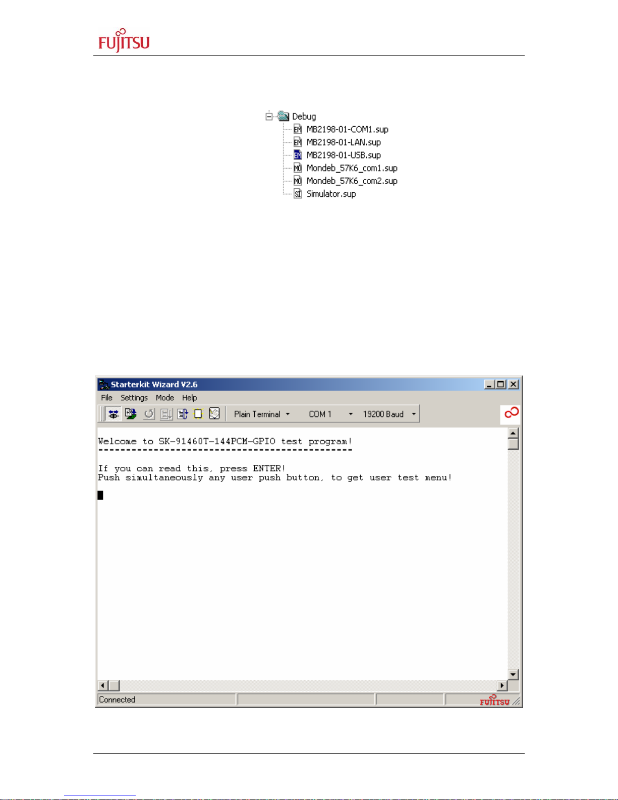
The SK-91460T-144PMC-GPIO is delivered with a SW-Application which allows the testing
of different functionalities.
Run Skwizard.bat, select 19200 baud. Connect UART4 (X2) of starterkit to the PC (e.g.
COM1). The Terminal Software Skwizard can be found on the DVD at “Software and
Utilities”.
Press the reset button (SW 6) on the starterkit and follow the instructions given at the
terminal.
Figure 5-3 Skwizard after reset of starterkit
Page 35

SK-91460T-144PMC-GPIO User Guide
Chapter 6 Programming the internal Flash
© Fujitsu Microelectronics Europe GmbH - 35 - FMEMCU-UG-910074-11
6 Programming the internal Flash
All Flash devices have an internal bootloader for asynchronous as well as synchronous
Flash-programming:
< Asynchronous serial Flash-programming via X2 (UART 4)
< Synchronous serial Flash-programming via X1
6.1 Asynchronous Mode
This chapter describes the serial asynchronous programming of the internal flash with the
help of the ‘FME-FR Programmer’ in automatic mode. For other programming possibilities,
please see the application note mcu-an-300012-e-mb91460_flash_programming.pdf.
1) For serial asynchronous programming SUB-D9 connector X2 which is connected to
UART4 has to be used. The following jumper setting is needed.
Jumper Setting Description
JP21
(RXD)
1-2 SIN4 is connected to RS232 transceiver
JP25
(TXD)
1-2 SOT4 is connected to RS232 transceiver
JP27
(RS232/LIN)
1-2 X2 Pin2 is connected to RS232 transceiver (T1out)
Table 6-1: Jumper Settings for Programming
Page 36

SK-91460T-144PMC-GPIO User Guide
Chapter 6 Programming the internal Flash
FMEMCU-UG-910074-11 - 36 - © Fujitsu Microelectronics Europe GmbH
2) If the programming software should generate a reset signal on RTS or DTR line, refer
to the following jumper list.
Jumper Setting Description
Closed RTS and CTS of X2 are connected JP20
(RTS-CTS)
Open RTS and CTS of X2 are not connected
1-2 DTR signal (Pin 6 of X2) is used as reset source JP89
(DTR/RTS)
2-3 RTS signal (Pin 7 of X2) is used as reset source
JP16
(RST 0/4)
Closed LIN-UART 4 (X2) connected to reset circuit
1-2 No negation for the DTR/RTS signal
JP13
(DTR / DTRx)
2-3 DTR/RTS signal is negated
JP38
(RST MCU)
Closed External reset generation is active
Table 6-2: Jumper Settings for reset signal
3) The CPU Mode selection must be set to internal reset vector mode by setting DIP
switch S1 to (Off, Off, Off, Off) (only if DIP Switch mounted!)
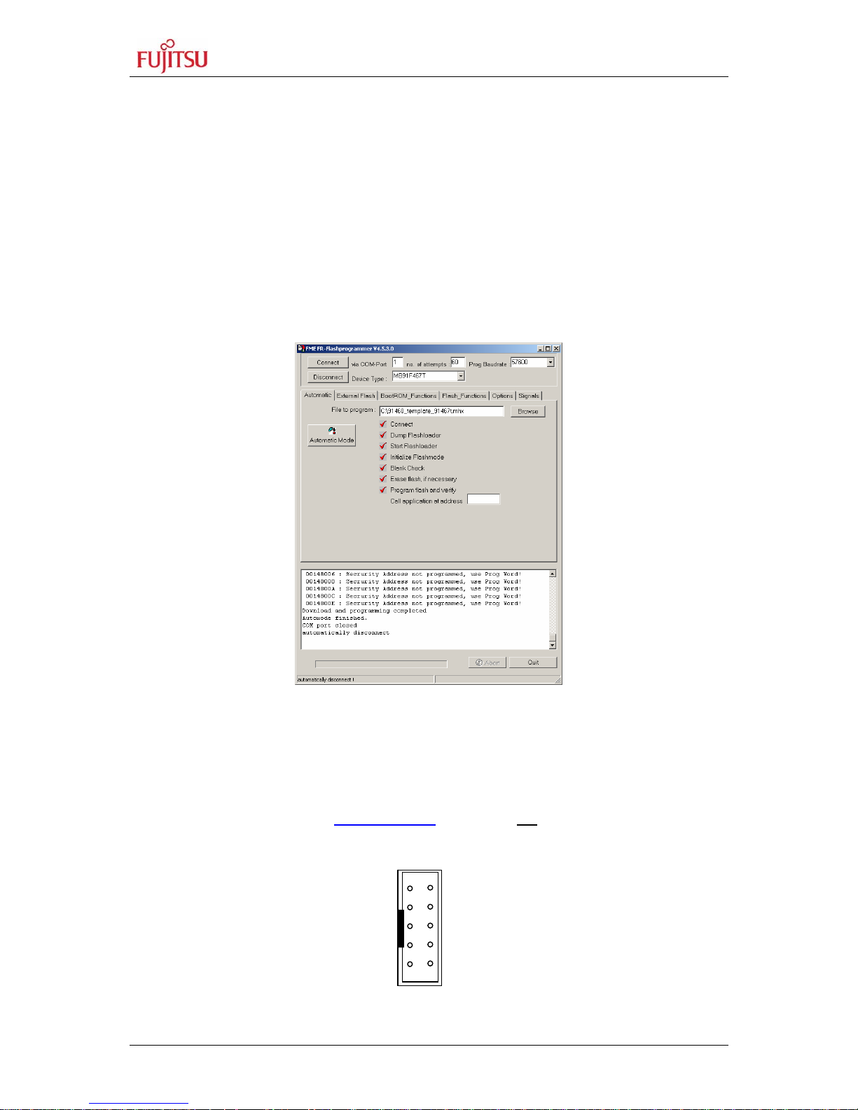
4) Start the ‘FME-FR Programmer’ and connect the UART4 to your serial PC
communication port. A straight cable connection has to be used.
5) Choose the microcontroller device (“MB91F467T”) as device type and browse to the
mhx-file you want to program to the embedded flash memory of the microcontroller.
Press the button “Automatic Mode” to start programming.
6) After that, immediately reset the microcontroller.
Page 37

SK-91460T-144PMC-GPIO User Guide
Chapter 6 Programming the internal Flash
© Fujitsu Microelectronics Europe GmbH - 37 - FMEMCU-UG-910074-11
Figure 6-1: Settings for Automatic Mode
7) If your hardware supports MCU reset via DTR or RTS signal lines of the PC’s COM
port, go to sheet “Signals” and select the appropriate reset signal line. The
programmer now resets the microcontroller automatically before starting the
programming sequence and you do not have to reset the MCU manually immediately
after pressing the button “Automatic Mode”.
Figure 6-2: Reset Signal Settings
RESET MCU
1.
3.
2.
Page 38
SK-91460T-144PMC-GPIO User Guide
Chapter 6 Programming the internal Flash
FMEMCU-UG-910074-11 - 38 - © Fujitsu Microelectronics Europe GmbH
The software now automatically writes a flash loader to the microcontroller, does a blank
check and erases the flash memory if necessary. After that the user application is
programmed to the embedded flash memory.
During this sequence the actual progress status can be seen by checked off steps on the
“Automatic” sheet and the messages below in the message box.
If the programming sequence is ended successfully, you will receive the output shown in
figure 7.
The Addresses 0x14:8000 to 0x14:800F cannot be written in automatic mode. This is a built
in security feature to prevent unintended writing to the Flash Security Vectors and Boot
Security Vectors. Otherwise it would be possible to secure flash content and to lock the
microcontroller for serial programming/reading/erasing by not being able to enter the internal
loader anymore. If you want to use these features explicitly, you have to program these
dedicated addresses by using the “Prog Word” Function of the step-by-step mode.
Figure 6-3: Successful Programming in Automatic Mode
6.2 Synchronous Mode
In order to program the Flash-ROM synchronously special third-party soft- and hardware has
to be used, e.g. GALEP-4 from www.conitec.de
. This tool is not available for free.
A dedicated Flash programming socket (X1) is provided on the evaluation-board for direct
connection to this programmer.
Figure 6-4: X1 Flash Programming Socket
n/c 1
n/c 3
RST 5
SOT4 7
VCC 9
2 n/c
4 n/c
6 SIN4
8 SCK4
10 GND
Page 39

SK-91460T-144PMC-GPIO User Guide
Chapter 7 Troubleshooting
© Fujitsu Microelectronics Europe GmbH - 39 - FMEMCU-UG-910074-11
7 Troubleshooting
Problem Solution
Starter-kit does not power-on correctly.
Some or all of the power LEDs (D20 and
D28) do not light.
Check voltage supply and jumpers :
∗ The voltage on DC-Power plug should be in the
range of 9-12V. The plug should have ‘+’ on shield
and ‘–‘ on the centre. The power supply should be
able to supply at least 500 mA. To support both,
the “SK-91F460T-144PMC-GPIO” and a graphic
sub-board the supply should be able to supply
1500mA.
* The LEDs should light up after switching on the
board. Use a millimetre to see whether 5V,3.3V,
are present on the Vcc/GND test measurement
points J9, J10.
∗ Check jumper positions according to chapter 2.2.
∗ Remove all user extensions of the starter-kit
Starter-kit stays in reset.
LED D10 (Reset indicator) lights up
permanently.
∗ LED D10 (Reset) should flash. If D10 lights up
permanently, the voltage is too low. Increase the
voltage supply and check available supply current
to solve the problem.
∗ Remove all user extensions on the board to avoid
any shortcuts or leakage current!
The communication from Softune
Workbench to the evaluation board fails
(Communication errors).
∗ Make sure your COM-port number and the baud
rate settings are correct (see debugger
introduction). The default COM-port is 1 and the
default baud rate is 57.6 kBaud.
∗ Make sure no other programs are using the same
COM-port on your PC. Close all other applications
(e.g. flash programmer utilities, terminals etc.)
* Check if RTS/CTS is closed on the CPU module
(check jumper JP21, 25, 20 are closed).
* Use only a RS232 extension 1:1 cable.
The windows of the debugger are empty. * This is due to wrong (maybe old) file path
information. Closing all windows in the debugger
and re-open should fix the problem.
When trying to program the application to
the embedded flash, the programmer
stops at first address with “loading error” !
* You are probably trying to program a program to
the flash which is linked for the external RAM area.
Check for details the linker memory map and the
linker output mapping file *.mp1 file.
Hardware units such as LEDs, user
buttons, UART are not working.
∗ Make sure you have enabled these units on the
evaluation board using the appropriate jumpers.
See the provided examples and the hardware
manual for information on how to control the
peripherals.
Optional LC-Display at J1 does not work
∗ Adjust the potentiometer RP1 to adjust contrast
of LCD. Remove resistor network RN1.
Graphic sub-board does not work Check power supply 9-12V/1500mA. Reduce
external bus clock frequency.
Page 40

SK-91460T-144PMC-GPIO User Guide
Chapter 8 Appendix
FMEMCU-UG-910074-11 - 40 - © Fujitsu Microelectronics Europe GmbH
8 Appendix
8.1 Related Products
< SK-91460T-144PMC-GPIO Evaluation board for the MB91F467TA MCU
in FPT-176P-M07 package
< MB2198-01 Emulator debugger main unit
< MB2198-10 DSU cable
EMA-MB91V460A-002B-80 Adapter board
< NQPACK144SD-ND Socket for package FPT-176P-M07
(Tokyo Eletech Corp)
http://www.tetc.co.jp/e_products/e_nq_techdrawings.htm
< EMA-MB91F467T-NLS-144M08 Emulator probe cable for MB91F467TA MCU
EMA-MB91F467T-LS-144M08
< MB91460 Series
< MB91F467TA-144PMC Flash MCU
Page 41

SK-91460T-144PMC-GPIO User Guide
Chapter 8 Appendix
© Fujitsu Microelectronics Europe GmbH - 41 - FMEMCU-UG-910074-11
8.2 Information in the WWW
Information about FUJITSU MICROELECTRONICS Products
can be found on the following Internet pages:
Microcontrollers (8-, 16- and 32bit), Graphics Controllers
Datasheets and Hardware Manuals, Support Tools (Hard- and Software)
http://mcu.emea.fujitsu.com/
http://www.fujitsu.com/emea/services/microelectronics/displaycontrollers/
Page 42

SK-91460T-144PMC-GPIO User Guide
Chapter 8 Appendix
FMEMCU-UG-910074-11 - 42 - © Fujitsu Microelectronics Europe GmbH
8.3 Tables
Table 1-1: Emulation System .................................................................................................8
Table 2-1: Jumper Settings .................................................................................................. 11
Table 3-1: MCU Operating Mode .........................................................................................14
Table 3-2: Power Switch ...................................................................................................... 15
Table 3-3: Power Supply Configuration................................................................................ 15
Table 3-4: Voltage Test Pins................................................................................................ 16
Table 3-5: ADC Supply ........................................................................................................ 17
Table 3-6: UART 4 Settings ................................................................................................. 18
Table 3-7: UART 5 Settings ................................................................................................. 19
Table 3-8: UART 6 Settings ................................................................................................. 20
Table 3-9: UART 7 Settings ................................................................................................. 21
Table 3-10: CAN Settings ....................................................................................................22
Table 3-11: Reset Connection.............................................................................................. 23
Table 3-12: User Push Buttons ............................................................................................ 24
Table 3-13: Potentiometer Settings...................................................................................... 24
Table 4-1: UART Connector Signals .................................................................................... 26
Table 4-2: CAN Connector Signals ...................................................................................... 26
Table 4-3: User LEDs/LCD................................................................................................... 27
Table 4-4: In-circuit programming connector ........................................................................ 28
Table 6-1: Jumper Settings for Programming....................................................................... 35
Table 6-2: Jumper Settings for reset signal.......................................................................... 36
Page 43

SK-91460T-144PMC-GPIO User Guide
Chapter 8 Appendix
© Fujitsu Microelectronics Europe GmbH - 43 - FMEMCU-UG-910074-11
8.4 Figures
Figure 2-1: Default Jumper Settings..................................................................................... 12
Figure 2-2: Softune Workbench Start Menu Location........................................................... 13
Figure 2-3: Softune Workbench V6 IDE ............................................................................... 13
Figure 3-1: MCU mode switch.............................................................................................. 14
Figure 3-2: Voltage Test Pins............................................................................................... 16
Figure 4-1: Power Connector ............................................................................................... 25
Figure 4-2: UART Connector................................................................................................ 26
Figure 4-3: CAN Connector.................................................................................................. 26
Figure 4-4: User LEDs/LCD ................................................................................................. 27
Figure 4-5: In-circuit programming connector....................................................................... 28
Figure 5-1: Softune Workbench main window ......................................................................29
Figure 5-2: Open Softune Workbench workspace (*.wsp).................................................... 32
Figure 5-3 Skwizard after reset of starterkit.......................................................................... 34
Figure 6-1: Settings for Automatic Mode .............................................................................. 37
Figure 6-2: Reset Signal Settings......................................................................................... 37
Figure 6-3: Successful Programming in Automatic Mode..................................................... 38
Figure 6-4: X1 Flash Programming Socket...........................................................................38
Page 44

SK-91460T-144PMC-GPIO User Guide
Chapter 8 Appendix
FMEMCU-UG-910074-11 - 44 - © Fujitsu Microelectronics Europe GmbH
8.5 Abbreviations
ADC Analogue Digital Converter
CAN Controller Area Network
CS Chip Select
FME Fujitsu Microelectronics Europe GmbH
LIN Local Interconnect Network
MCU Microcontroller Unit
PCB Printed Circuit Board
SRAM Static Random Access Memory
UART Universal Asynchronous Receiver Transmitter
Page 45

SK-91460T-144PMC-GPIO User Guide
Chapter 9 China-RoHS regulation
© Fujitsu Microelectronics Europe GmbH - 45 - FMEMCU-UG-910074-11
9 China-RoHS regulation
Evaluation Board
评估板
Emulation Board
仿真板
根据SJ/T11364-2006
《电子信息产品污染控制标识要求》特提供如下有关污染控制方面的信息。
The following product pollution control information is provided according to SJ/T11364-2006
Marking for Control of Pollution caused by Electronic Information Products.
1.电子信息产品污染控制标志说明 Explanation of Pollution Control Label
该标志表明本产品含有超过中国标准SJ/T11363-2006
《电子信息产品中有毒有害物质的限量要求》中限量的有毒有害物质。标志中的数字为本产品
的环保使用期,表明本产品在正常
使用的条件下,有毒有害物质不会发生外泄或突变,用户使
用本产品不会对环境造成严重污染或对其人身、财产造成严重损害的期限,单位为年。
为保证所申明的环保使用期限,应按产品手册中所规定的环境条件和方法进行正常使用,并严
格遵守产品维修手册中规定的定期维修和保养要求。
产品中的消耗件和某些零部件可能有其单独的环保使用期限标志,并且其环保使用期限有可能
比整个产品本身的环保使用期限短。应到期按产品维修程序更换那些消耗件和零部件,以保证
所申明的整个产品的环保使用期限。
本产品在使用寿命结束时不可作为普通生活垃圾处理,应被单独收集妥善处理。
请注意:环保使用期限50年的指定不是与产品的耐久力,使用期限或任何担保要求等同的。
This symbol to be added to all EIO sold to China, indicates the product contains hazardous
materials in excess of the limits established by the Chinese standard SJ/T11363-2006
Requirements for Concentration Limits for Certain Hazardous Substances in Electronic
Information Products. The number in the symbol is the Environment-friendly Use Period
(EFUP), which indicates the period, starting from the manufacturing date, during which the
toxic or hazardous substances or elements contained in electronic information products will
not leak or mutate under normal operating conditions so that the use of such electronic
information products will not result in any severe environmental pollution, any bodily injury or
damage to any assets, the unit of the period is “Year”.
Page 46

SK-91460T-144PMC-GPIO User Guide
Chapter 9 China-RoHS regulation
FMEMCU-UG-910074-11 - 46 - © Fujitsu Microelectronics Europe GmbH
In order to maintain the declared EFUP, the product shall be operated normally according to
the instructions and environmental conditions as defined in the product manual, and periodic
maintenance schedules specified in Product Maintenance Procedures shall be followed
strictly.
Consumables or certain parts may have their own label with an EFUP value less than the
product. Periodic replacement of those consumables or parts to maintain the declared EFUP
shall be done in accordance with the Product Maintenance Procedures.
This product must not be disposed of as unsorted municipal waste, and must be collected
separately and handled properly after decommissioning.
Please note: The designation of 10 years EFUP is not
to be equated with the durability, use-
duration or any warranty-claims of the product.
产品中有毒有害物质或元素的名称及含量
Table of hazardous substances name and concentration
有毒有害物质或元素
Hazardous substances name
部件名称
Component Name
铅
(Pb)
汞
(Hg)
镉
(Cd)
六价铬
(Cr(VI))
多溴联苯
(PBB)
多溴二苯醚
(PBDE)
SK-91460T-144PMC-GPIO
x o o o o o
O: 表示该有毒有害物质在该部件所有均质材料中的含量均在SJ/T11363-2006 标准规定的限量要求以下
X: 表示该有毒有害物质至少在该部件的某一均质材料中的含量超出SJ/T11363-2006 标准规定的限量要求
• 此表所列数据为发布时所能获得的最佳信息
• 由于缺少经济上或技术上合理可行的替代物质或方案,此医疗设备运用以上一些有毒有害物质来实现设备的预期
临床功能,或给人员或环境提供更好的保护效果
。
O: Indicates that this toxic or hazardous substance contained in all of the homogeneous
materials for this part is below the limit requirement in SJ/T11363-2006.
X: Indicates that this toxic or hazardous substance contained in at least one of the
homogeneous materials used for this part is above the limit requirement in SJ/T11363-2006.
• Data listed in the table represents best information available at the time of publication
Page 47

SK-91460T-144PMC-GPIO User Guide
Chapter 10 Recycling
© Fujitsu Microelectronics Europe GmbH - 47 - FMEMCU-UG-910074-11
10 Recycling
Gültig für EU-Länder:
Gemäß der Europäischen WEEE-Richtlinie und deren Umsetzung in landesspezifische
Gesetze nehmen wir dieses Gerät wieder zurück.
Zur Entsorgung schicken Sie das Gerät bitte an die folgende Adresse:
Fujitsu Microelectronics Europe GmbH
Warehouse/Disposal
Monzastraße 4a
63225 Langen
Valid for European Union Countries:
According to the European WEEE-Directive and its implementation into national laws we
take this device back.
For disposal please send the device to the following address:
Fujitsu Microelectronics Europe GmbH
Warehouse/Disposal
Monzastraße 4a
63225 Langen
 Loading...