

Page 1
SCARLET
Subboard
Documentation
Fujitsu Microelectronics Europe GmbH
Am Siebenstein 6-10
63303 Dreieich-Buchschlag, Germany
Page 2

2
History
Revision Date Comment
V1.0 12.03.01 New Document
V1.1 06.06.01 Update (redesign of board)
V1.2 05.07.01 New board plan
Page 3

3
Warranty and Disclaimer
To the maximum extent permitted by applicable law, Fujitsu Microelectronics Europe GmbH restricts its
warranties and its liability for all products delivered free of charge (e.g. software include or header files,
application examples, target boards, evaluation boards, engineering samples of IC’s etc.), its performance
and any consequential damages, on the use of the Product in accordance with (i) the terms of the License
Agreement and the Sale and Purchase Agreement under which agreements the Product has been delivered,
(ii) the technical descriptions and (iii) all accompanying written materials. In addition, to the maximum
extent permitted by applicable law, Fujitsu Microelectronics Europe GmbH disclaims all warranties and
liabilities for the performance of the Product and any consequential damages in cases of unauthorised
decompiling and/or reverse engineering and/or disassembling. Note, all these products are intended and
must only be used in an evaluation laboratory environment.
1. Fujitsu Microelectronics Europe GmbH warrants that the Product will perform substantially in
accordance with the accompanying written materials for a period of 90 days form the date of
receipt by the customer. Concerning the hardware components of the Product, Fujitsu
Microelectronics Europe GmbH warrants that the Product will be free from defects in material and
workmanship under use and service as specified in the accompanying written materials for a
duration of 1 year from the date of receipt by the customer.
2. Should a Product turn out to be defect, Fujitsu Microelectronics Europe GmbH entire liability and
the customer’s exclusive remedy shall be, at Fujitsu Microelectronics Europe GmbH sole
discretion, either return of the purchase price and the license fee, or replacement of the Product or
parts thereof, if the Product is returned to Fujitsu Microelectronics Europe GmbH in original
packing and without further defects resulting from the customer’s use or the transport. However,
this warranty is excluded if the defect has resulted from an accident not attributable to Fujitsu
Microelectronics Europe GmbH, or abuse or misapplication attributable to the customer or any
other third party not relating to Fujitsu Microelectronics Europe GmbH.
3. To the maximum extent permitted by applicable law Fujitsu Microelectronics Europe GmbH
disclaims all other warranties, whether expressed or implied, in particular, but not limited to,
warranties of merchantability and fitness for a particular purpose for which the Product is not
designated.
4. To the maximum extent permitted by applicable law, Fujitsu Microelectronics Europe GmbH and
its suppliers´ liability is restricted to intention and gross negligence.
NO LIABILITY FOR CONSEQUENTIAL DAMAGES
To the maximum extent permitted by applicable law, in no event shall Fujitsu
Microelectronics Europe GmbH and its suppliers be liable for any damages whatsoever
(including but without limitation, consequential and/or indirect damages for personal injury,
assets of substantial value, loss of profits, interruption of business operation, loss of
information, or any other monetary or pecuniary loss) arising from the use of the Product.
Should one of the above stipulations be or become invalid and/or unenforceable, the remaining stipulations
shall stay in full effect.
Page 4

4
Important notice
This Starterkit contains an evaluation board, documentation and software on a CD-ROM.
For documentation or software updates, please refer to our web site www.fujitsu-fme.com !
Fujitsu reserves the right to make changes to its products or to discontinue any semiconductor
product or service without notice.
12.03.01 V1.0
Page 5

5
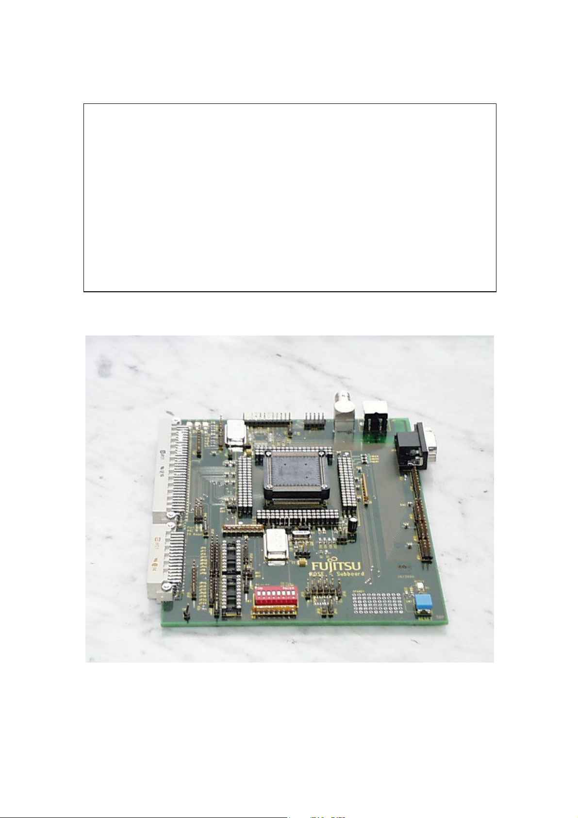
1. Introduction
The SCARLET-Subboard is a low cost multifunctional evaluation board for Fujitsu graphic device
controller Scarlet. It can be used with CREMSON-Starterkit CPU-Modul for software development and
testing as a simple target board.
The board allows the designer immediately to start the software development before his own final target
system is available.
2. Features
• Graphic controller Scarlet in a package HQFP208
• 14.318 MHz crystal and 14.318 MHz oscillator
• Enhanced Video Input Processor (SAA7111A)
Quarzoszilator for VIC
•
• Video input connector (BNC-90)
• 2 PALLV16V8
a 74ALS1034 (six not inverted buffer)
•
• 3 LEDs for power supply
• Display interface (HD-DSUB-BU-15Pol)
• “CPU-Modul” interface
Reset button for Scarlet
•
Page 6

6
3. Jumpers and Switches
This chapter describes all jumpers and switches which can be modified on the evaluation board. The default
setting is shown with a gray shaded area. All jumpers and switches are named directly on the board by its
meaning, so it is very easy to set the jumpers according to the features.
3.1 Power Supply Voltage (JP1, JP2, JP4, JP20)
3V3 power supply
(JP1)
Jumper setting Description
ON (closed) Power supply
OFF (open) NO Power supply
2V5 power supply
(JP2)
2V5 power supply
(JP4)
2V5 power supply
(JP20)
NOTE:
The supply voltage for the core and the IO Pins must be set. Otherwise it could happen that the
controller does not work correctly!
Jumper setting Description
ON (closed) Power supply
OFF (open) NO Power supply
Jumper setting Description
ON (closed) Power supply
OFF (open) NO Power supply
Jumper setting Description
ON (closed) Analog Power supply
OFF (open) NO Analog Power supply
Page 7

7
3.2 Define graphic controller Operating Mode (SW3)
The Scarlet can be connected to Fujitsu FR30, Hitachi SH4(SH7750), SH3(SH7709/09A) and NEC V832.
The host CPU type is specified by the MODE pins.
CPU Type SW3/Mode0 SW3/Mode1
FR30/SH3 ON ON
SH4 OFF ON
Mode1-0
V832 ON OFF
Reserved OFF OFF
SW3/Mode2 Description
ON XRDY signal finished at low level
Mode2
OFF XRDY signal finished at high level
SW3/CKM Description
ON Output from internal PLL is selected
Clock mode signal
OFF Host CPU bus clock is selected
SW3/EO Description
Even/Odd signal
mode
Clock Input SW3/CLKSEL0 SW3/CLKSEL1
Input Clock
Selection
SW3/OSCCNT Description
Oscillator control
ON
OFF
13.5 MHz ON ON
14.32 MHz OFF ON
17.73 MHz ON OFF
Reserved OFF OFF
ON
OFF
Low level output in even frame, High
level output in odd frame
High level output in even frame, Low
level output in odd frame
Control of internal clock-module
(should be H-level)
Page 8

8
3.3 Reset Pin (JP29)
The Jumper JP212 determines the Scarlet Reset Pin.
It can be connected directly with the Reset of the VGC, or with a port of the MCU, to execute a software
Reset.
JP29 Description
1-2 Reset from CPU-board
Reset
2-3
3.4 Video Input Processor (JP5, JP47, JP30)
JP5 Description
Power supply
voltage
JP47 Description
VIC enable
On (closed)
OFF (open) NO power supply
1-2 VCC – VIC enable
2-3 GND – VIC disable
Using port S0 from
MCU
Digital and analog
supply voltage for VIC
JP30 Description
I2C-Bus slave
address select
JP57 Description
(SDA)
JP27 Description
I2C-Serial clock line
(SCL)
JP58 Description
VIC signal
GND (closed)
VCC (open)
1-2
2-3
1-2
2-3
ON (closed)
OFF (open) More than 75 Ohm
0 = 48h for write,
49h for read
1 = 4Ah for write,
4Bh for read
Serial data line from
MCU I2C-Interface I2C-Serial data line
Serial data line from
Scarlet I2C-Interface
Serial clock line from
MCU I2C-Interface
Serial clock line from
Scarlet I2C-Interface
Conclusion resistance
75 Ohm
Page 9

9
3.5 Clock Settings (JP42, JP43, JP44)
JP42 Description
1-2
Clock input enable
2-3
JP43 Description
ON (closed) Crystal enable
Crystal Y2
OFF (open) Crystal disable
JP44 Description
1-2
PLL power supply
2-3
3.6 C-sync for display (JP5)
JP5 Description
ON (closed)
C-sync
OFF (open) C-sync not connected
Scarlet clock from
Oscillator Y1
Scarlet clock from
Crystal Y2
PLLVDD connect to
core voltage
PLLVDD connect to
separated voltage
C-sync connected to
VGA connector
3.7 PAL Settings (JP6, JP7, JP8, JP9, JP10, JP11, JP12, JP13, JP14, JP15, JP16, JP17, JP18, JP19,
JP50, JP24)
JP6 Description
Needed for internal state
machine Bus clock for
Wait request from
Scarlet
PALLV16V8
Wait request
Read strobe
ON (closed)
OFF (open) -
JP7 Description
ON (closed)
OFF (open) -
JP8 Description
ON (closed) Read signal to Scarlet
OFF (open) -
Page 10

10
JP11 Description
Write strobe
Write strobe
Write strobe
Write strobe
ON (closed) Write signal D0 – D7
XWE0
JP12 Description
XWE1
JP13 Description
XWE2
JP14 Description
XWE3
JP9 Description
OFF (open) -
ON (closed) Write signal D8 – D15
OFF (open) -
ON (closed) Write signal D16 – D23
OFF (open) -
ON (closed) Write strobe D24 – D31
OFF (open) -
DMA acknowledge
JP10 Description
DMA end operation
JP15 Description
Bus clock for
PALLV16V8
JP16 Description
CS3
ON (closed)
OFF (open)
ON (closed)
OFF (open)
ON (closed)
OFF (open)
ON (closed)
OFF (open)
Not needed for internal
logic
Not needed for internal
logic
Not needed for internal
logic
CS3 for PAL logic
enable
CS3 for PAL logic
disable
Page 11

11
JP17 Description
ON (closed)
CS4
OFF (open)
JP18 Description
ON (closed)
CS5
OFF (open)
JP19 Description
ON (closed)
CS6
OFF (open)
JP50 Description
ON (closed) PAL Reset from VGC
PAL Reset
OFF (open) -
CS4 for PAL logic
CS4 for PAL logic
CS5 for PAL logic
CS5 for PAL logic
CS6 for PAL logic
CS6 for PAL logic
enable
disable
enable
disable
enable
disable
JP24 Description
Reset Switch
3.7 Interrupt
JP21 / JP52 Description
Interrupt enable
3.8 DMA
JP23 / JP54 Description
DREQ0 enable
ON (closed) Reset from switch SW1
OFF (open) -
ON (closed)
OFF (open) -No connected
ON (closed)
OFF (open) -No connected
Connected interrupt to
MCU
Connected DREQ0 to
MCU
Page 12

12
3.9 Header for Debug Signals
PWM (JP25)
• PortS7-1 - Free usable Port S (bit 1..7)
Display Signals (JP45)
• RTC0 - Real time control output
• RTS0 - PAL line identifier (SAA7111A)
• RTS1 - PAL line identifier (SAA7111A)
• V
•
• C
- Vertical reference output signal
ref
H
- Horizontal reference output signal
ref
- Clock reference output
ref
• HS - Horizontal sync output signal
• VS - Vertical sync output signal
GPSW - General purpose switch output
•
• RES-out - Reset output (active low)
Power Supply Voltage (JP49)
Power supply voltage (2V5, 3V3, 5V0) – GND
•
Video Input Processor Signals (JP84)
• SAA_VI7-0 - Digital Video Port Out-Bus from SAA7111A
VI_CLK - Line-locked System Clock Output (27MHz) from SAA7111A
•
Chip Select Signals(JP28)
• CS0-6 - Chip Select from MCU
Buffer signals (JP34, JP35, JP36, JP37, JP38, JP39, JP40, JP41)
• I/O Pins for 74ALS1034 (six not inverted buffer)
Digital RED (JP31)
• R0-7 - Digital signal output (RED)
Digital GREEN (JP32)
• G0-7 - Digital signal output (GREEN)
Digital BLUE (JP33)
B0-7 - Digital signal output (BLUE)
•
Analog Output (JP46)
• DCLK_OUT - Dot Clock Signal for Display
DCLK_IN - Dot Clock Input for External Synchronization
•
• RED - Analog signal output (RED)
• GREEN - Analog signal output (GREEN)
Page 13

13
• BLUE - Analog signal output (BLUE)
• H_SYNC - Horizontal sync signal output
V_SYNC - Vertical sync signal output
•
• C_SYNC - Composite sync signal output
• GV - Video/Graphics Switch
PAL Output Pins (JH1, JH2, JP22, JP51, JP53)
• Not used in internal Logic
VIC Signal (JP59, JP60)
• Second connection for the video camera (video-in and camera GND)
For more information please look at the Hardware Manual of the Scarlet graphic controller, the Data Sheet
of the Video Input Processor SAA7111A and the Data Sheet of the PALLV16V8.
Page 14

14
4. Schematics and Drawings
Page 15

5
JDR1A
DIN 96_ABC-R
Vcc2V5_1
A1
A1
Vcc3V3
A2
A2
Vcc5V0
A3
A3
A4
A4
D0
A5
A5
D3
A6
A6
D6
A7
A7
D9
A8
A8
D12
A9
A9
D15
A10
A10
D18
A11
A11
D21
A12
A12
D24
A13
A13
D27
D D
C C
A14
A14
A15
A15
A16
A16
A17
A17
A18
A18
A19
A19
A20
A20
A21
A21
A22
A22
A23
A23
A24
A24
A25
A25
A26
A26
A27
A27
A28
A28
A29
A29
A30
A30
A31
A31
A32
A32
JDR2A
DIN 48_ABC-R
A1
A1
A2
A2
A3
A3
A4
A4
A5
A5
A6
A6
A7
A7
A8
A8
A9
A9
A10
A10
A11
A11
A12
A12
A13
A13
A14
A14
A15
A15
A16
A16
D30
A3
A6
A9
A12
A15
A18
PortS0
PortS3
PortS6
CS0
CS2
CS4
CS6
RDX
WR1
WR3
DREQ0
DEOP0
Interrupt_A
FR_Reset
JDR1B
DIN 96_ABC-R
B1
B1
B2
B2
B3
B3
B4
B4
B5
B5
B6
B6
B7
B7
B8
B8
B9
B9
B10
B10
B11
B11
B12
B12
B13
B13
B14
B14
B15
B15
B16
B16
B17
B17
B18
B18
B19
B19
B20
B20
B21
B21
B22
B22
B23
B23
B24
B24
B25
B25
B26
B26
B27
B27
B28
B28
B29
B29
B30
B30
B31
B31
B32
B32
JDR2B
DIN 48_ABC-R
B1
B1
B2
B2
B3
B3
B4
B4
B5
B5
B6
B6
B7
B7
B8
B8
B9
B9
B10
B10
B11
B11
B12
B12
B13
B13
B14
B14
B15
B15
B16
B16
Vcc2V5_1
Vcc3V3
Vcc5V0
D1
D4
D7
D10
D13
D16
D19
D22
D25
D28
D31
A4
A7
A10
A13
A16
A19
PortS1
PortS4
PortS7
Vcc2V5_3Vcc2V5_2
JDR1C
DIN 96_ABC-R
C1
C1
C2
C2
C3
C3
C4
C4
C5
C5
C6
C6
C7
C7
C8
C8
C9
C9
C10
C10
C11
C11
C12
C12
C13
C13
C14
C14
C15
C15
C16
C16
C17
C17
C18
C18
C19
C19
C20
C20
C21
C21
C22
C22
C23
C23
C24
C24
C25
C25
C26
C26
C27
C27
C28
C28
C29
C29
C30
C30
C31
C31
C32
C32
JDR2C
DIN 48_ABC-R
C1
C1
C2
C2
C3
C3
C4
C4
C5
C5
C6
C6
C7
C7
C8
C8
C9
C9
C10
C10
C11
C11
C12
C12
C13
C13
C14
C14
C15
C15
C16
C16
Vcc2V5_1
Vcc3V3
D2
D5
D8
D11
D14
D17
D20
D23
D26
D29
A2
A5
A8
A11
A14
A17
A20
PortS2
PortS5
CS1
CS3
CS5
FR_WAIT
WR0
WR2
AS
Bus_CLK
DACK0
I2C_SDA
I2C_SCL
Vcc3V3
12
C
SW3
1
16
2
15
3
14
4
13
JP61
5
6
7
8
SW DIP-8
B B
Bus_CLK
JP6
1 2
SCARLET_WAIT
JP7
1 2
RDX
JP8
1 2
WR0
JP11
1 2
WR1
JP12
1 2
WR2
JP13
1 2
WR3
JP14
1 2
DACK0
JP9
1 2
PAL_CS
1
JH2
2
HEADER 2
JP29
FR_Reset
1
PAL_RES_in
2
PortS0
3
RES_select
Bus_CLK
CS3
CS4
CS5
PAL_RES_in
Reset_SW
A A
JP22
HEADER 3
JP15
1 2
JP16
1 2
JP17
1 2
JP18
1 2
JP19
1 2
JP50
1 2
JP24
1 2
1
2
3
R26
10k
1 2
12
EO-pin
11
10
9
Vcc3V3
U4
2010
16V8 (Sockel)
1
I0
F0
2
VCCGND
I1
F1
3
I2
F2
4
I3
F3
5
I4
F4
6
I5
F5
7
I6
F6
8
I7
F7
9
I8
11
I9
1 2
12
FR_WAIT
13
PAL_DRACK
14
PAL_DTACK
15
16
17
18
19
Vcc3V3
U7
2010
16V8 (Sockel)
1
I0
2
VCCGND
I1
3
I2
4
I3
5
I4
6
I5
7
I6
8
I7
9
I8
11
I9
PAL_A21
12
F0
PAL_A22
13
F1
PAL_A23
14
F2
PAL_A24
15
F3
PAL_CSCS6
16
F4
PAL_Reset
17
F5
18
F6
19
F7
R2
8 x 47k
3456789
SCARLET_MODE0
SCARLET_MODE1
SCARLET_MODE2
SCARLET_CKM
SCARLET_EO
CLKSEL0
CLKSEL1
OSCCNT
DEOP0
JP10
JP53
1
HEADER 4
2
3
4
JP51
1
HEADER 2
2
4
Vcc2V5_1
Vcc3V3
Vcc5V0
JP25
PortS1
1
PortS2
2
PortS3
3
PortS4
4
PortS5
5
PortS6
6
PortS7
7
8
PortS1..7
JP28
CS0
1
CS1
2
CS2
3
CS3
4
CS4
5
CS5
6
CS6
7
8
CS0..6
FR_SDA
FR_SCL
R3
Vcc3V3 PAL_CS
1 2
3
4
5
6
7
8
9
C
8 x 47k
Vcc3V3
R15
15k
SW1
SCARLET_RESET
C55
100nF
Vcc2V5_1
Vcc3V3
Vcc5V0
Interrupt_A
DREQ0
DACK0
DEOP0
res-4
res-5
R27
470
D1
SCARLET_Reset
D0
56
D1
57
D2
58
D3
59
D4
60
D5
61
D6
62
D7
63
D8
66
D9
67
D10
68
D11
69
D12
70
D13
71
D14
72
D15
75
D16
76
D17
77
D18
78
D19
80
D20
81
D21
82
D22
83
D23
84
D24
85
D25
88
D26
89
D27
90
D28
91
D29
92
D30
95
D31
96
A2
133
A3
134
A4
135
A5
136
A6
137
A7
138
A8
161
A9
162
A10
163
A11
164
A12
165
A13
166
A14
167
A15
168
A16
171
A17
172
A18
173
A19
174
A20
175
PAL_A21
176
PAL_A22
177
PAL_A23
178
PAL_A24
179
Vcc3V3 TESTH0
Reset_SW
SAA_VI0
SAA_VI2
SAA_VI4
SAA_VI6
VI_CLK
D0
D1
D2
D3
D4
D5
D6
D7
D8
D9
D10
D11
D12
D13
D14
D15
D16
D17
D18
D19
D20
D21
D22
D23
D24
D25
D26
D27
D28
D29
D30
D31
A2
A3
A4
A5
A6
A7
A8
A9
A10
A11
A12
A13
A14
A15
A16
A17
A18
A19
A20
A21
A22
A23
A24
Vss-1
161522323947525465748693
R31
1 2
C
8 x 47k
SCARLET_XINT
SCARLET_DREQ
JP48
12
34
56
78
910
dig. VIDEO-in
SCARLET_MODE0
SCARLET_MODE2
SCARLET_MODE1
45464944113
MODE0
MODE1
Vss-2
Vss-3
Vss-4
Vss-5
3
4
5
6
7
8
9
1 2
1 2
PAL_Reset
Bus_CLK
XRST
BCLKI
MODE2
Vss-6
Vss-7
Vss-8
TESTH1
TESTH2
TESTH3
TESTH4
TESTH5res-3
JP21
JUMPER
JP23
JUMPER
AS
115
XBS
Vss-9
SAA_VI1
SAA_VI3
SAA_VI5
SAA_VI7
RDX
PAL_CS
114
XCS
Vss-10
116
XRD
Vss-11
WR2
WR3
117
118
XWE0
Vss-12
3
R0
R2
R4
R6
SCARLET_WAIT
WR0
WR1
119
1209798
XWE1
XWE2
XWE3
Vss-13
Vss-14
Vss-15
100
111
122
D_GND
1 2
3 4
SCARLET_XINT
PAL_DTACK
PAL_DRACK
SCARLET_DREQ
107
108
99
XINT
XRDY
DREQ
DTACK
DRACK
Vss-16
Vss-17
Vss-18
Vss-19
Vss-20
125
131
140
157
169
A_GND
RGND
0R0
D_GND
U11A
74ALS34
U11B
74ALS34
JP31
12
34
56
78
910
RED-out
SAA_VI0
VI_CLK
193
182
CCLK
Vss-21
Vss-22
Vss-23
Vss-24
Vss-25
180
191
203
208
SAA_VI2
SAA_VI1
194
195
VI0
VI1
VI2
VDDI-1
VDDI-2
1738557387
JP52
1 2
JUMPER
JP54
1 2
JUMPER
R1
R3
R5
R7
SAA_VI3
SAA_VI4
196
197
VI3
VI4
U9
SCARLET
VDDI-3
VDDI-4
SAA_VI5
SAA_VI6
198
199
VI5
VDDI-5
101
JP32
G0
12
G2
34
G4
56
G6
78
910
GREEN-out
SAA_VI7
R2
158
R3
VDDI-11
VDDI-12
170
R5
R4
R6
VDDI-13
192
251316374048
VCC0
R7
R7
VCC1
VCC2
G1
G2
G0
G0G1G2G3G4G5G6
VCC3
VCC4
VCC
JP4
VCC
1 2
Vcc2V5_2
R0
R1
34789101112181920212324252628293031333435
200
R0R1R2R3R4R5R6
VI6
VI7
VDDI-6
VDDI-7
VDDI-8
VDDI-9
VDDI-10
112
121
132
139
VDDI
JP2
VDDI
1 2
Vcc2V5_1
Interrupt_A
Vcc5V0
C44
100nF
DREQ0
VCC5
G3
G4
VCC6
51
G1
G3
G5
G7
G6
G5
G7
G7
VDDE-1
VDDE-2
VCC7
142741647994110
JP39
1
2
HEADER 2
JP34
1
2
HEADER 2
JP38
1
2
HEADER 2
JP35
1
2
HEADER 2
2
B0
B2
B4
B6
B2
B0
B0B1B2B3B4B5B6
VDDE-3
VDDE-4
VDDE-5
VDDE-6
VDDE-7
VDDE
JP1
VDDE
1 2
Vcc3V3
11 10
13 12
JP33
12
34
56
78
910
BLUE-out
B7B5B4B3B1
B6
36
B7
VDDE-8
VDDE-9
VDDE-10
VDDE-11
126
159
181
201
U11C
5 6
74ALS34
U11D
9 8
74ALS34
U11E
74ALS34
U11F
74ALS34
DCLKO
DCLKI
AOUTR
AOUTG
AOUTB
HSYNC
VSYNC
CSYNC
VREF
ACOMPR
ACOMPG
ACOMPB
<open>
AVD3
AVD2
AVD1
AVD0
AVS3
AVS2
AVS1
AVS0
PLLVDD
PLLVSS
OSCOUT
OSCCNT
CLKSEL0
CLKSEL1
TESTH0
TESTH1
TESTH2
TESTH3
TESTH4
TESTH5
TESTL0
TESTL1
reserved-1
reserved-2
reserved-3
reserved-4
reserved-5
1
VGA-Stecker (SUB-D 15, 3reihig, weiblich)
JP46
C1
0.1uF
C54
100nF
SCARLET_SDA
SCARLET_SCL
Vcc3V3
DCLK_OUT
DCLK_IN
RED
GREEN
BLUE
H_SYNC
V_SYNC
C_SYNC
GV
A_GND
C2
0.1uF
C56
100nF
R32 10k
R33 10k
B1
B3
B5
B7
DCLK_OUT
202
DCLK_IN
190
RED
152
GREEN
147
BLUE
143
H_SYNC
206
V_SYNC
205
C_SYNC
204
SCARLET_EO
189
EO
GV
207
GV
155
156
145
141
154
VRO
CLK
CKM
R4
109
2.7k
153
149
146
C28
142
151
100nF
150
148
A_GND
144
PLLVDD
127
129
S
A_GND
130
CLKIN
124
OSCOUT
128
OSCCNT
123
CLKSEL0
42
CLKSEL1
43
SCARLET_CKM
106
TESTH0
53
TESTH1
102
TESTH2
103
TESTH3
104
TESTH4
105
TESTH5
183
TESTL0
50
TESTL1
160
184
185
res-3
186
res-4
187
res-5
188
PLLVDD-select
Vcc3V3
JP41
1
2
HEADER 2
JP36
1
2
HEADER 2
JP40
1
2
HEADER 2
JP37
1
2
HEADER 2
C58
22pF
100pF
A_GND
C5
JP44
C3
0.1uF
C57
100nF
R7
100k
A_GND
1
2
3
Y1
Oszillator_14.318MHz
5 6
R16
1M
Y2
14.318MHz
Vcc3V3
1
2
3
4
5
6
7
8
9
10
11
Analog-out
R5
750
R6
330
JP20
1 2
VCC_analog
Vcc3V3
D_GND
C29
100nF
+
D_GND
34
12
1 2
C_SYNC
C4
47uF
JP42
OSC-select
1 2
C59
22pF
JP55
A_GND
Vcc2V5_2
Vcc2V5_1
PLLVDD
Vcc2V5_3
1
2
3
JP43
Y2-out
RED
GREEN
BLUE
H_SYNC
V_SYNC
+
C40
Tantal n.b.
CLKIN
OSCOUT
JP3
1
2
3
4
5
6
7
8
9
10
11
12
13
14
15
BOHR98
BOHR99
VDDI
C6
C7
C8
C9
C10
C11
C12
C13
C14
22nF
22nF
22nF
22nF
22nF
22nF
22nF
5
C15
22nF
22nF
22nF
C31
C16
C17
22nF
22nF
22nF
4
VCC
C32
C33
C34
C35
C36
C37
C38
22nF
22nF
22nF
22nF
22nF
C39
22nF
22nF
22nF
3
VDDE
C18
C19
C20
C21
C22
C23
C24
C25
C26
C27
C30
Title
22nF
22nF
22nF
22nF
22nF
22nF
22nF
22nF
22nF
22nF
22nF
2
SCARLET-Subboard (CREMSON-Starterkit), FUJ22b
Size Document Number Rev
SCARLET-Subboard / SCARLET 1.1
C
Date: Sheet
1
of
12Thursday, April 05, 2001
Page 16

Vcc2V5_1
Vcc3V3
Vcc5V0
Vcc3V3
Vcc2V5_1
Vcc3V3
Vcc5V0
Vcc5V0
JP49
12
34
56
Vcc2V5_1
Vcc3V3
Vcc5V0
Vcc
78
1
Vcc2V5_1
Vcc2V5_1
Vcc3V3
Vcc5V0
R30
R29
R28
D4
2V5
270
470
D3
3V3
1k
D2
5V0
1234567891011
JP45
RTC0
RTS0
RTS1
Vref
Href
Vcc3V3
CrefVSGPSW
12
Peripheral
HS
RES-out
TP1
SAA_VCC
SAA_enable
1
GND
Title
of
22Thursday, April 05, 2001
1
SCARLET-Subboard / SAA7111 1.1
SCARLET-Subboard (CREMSON-Starterkit), FUJ22b
B
Size Document Number Rev
Date: Sheet
R20 1k
123
JP47
SAA_CLK
34
Y3
SAA_VCC
Vcc3V3
R25
SAA_Enable
2
12
24.5760MHz
5 6
10k
I2C_SA
JP30
I2C_Adr_sel
1 2
3
RES-out
23
/RES
VddD5
VddD4
VddD3
VddD2
VddD1
VddA2
VddA1
VddA0
VssD5
VssD4
VssD3
VssD2
VssD1
VssA2
VssA1
VssA0
Vsss
Vcc3V3
JP5
1 2
SAA_VCC
18
25
33
41
57
7
11
15
19
26
32
40
56
5
9
16
13
SAA_VCC
D_GND
SAA_VI6
SAA_VI3
SAA_VI5
SAA_VI4
SAA_VI2
VPO10
VPO11
VPO12
AI11
AI12
121410
SAA_Y_in
SAA_COMP_in
SAA_VI7
34
VPO13
VPO14
VPO15
U10
AI22
AI21
6
8
SAA_C_in
R24 75
VS
HS
27
30
VS
HS
SAA7111A
Vref
17
31
Vref
Href
CE
24
52
/FEI
29
28
RTS0
RTS1
60
RTC0
GPSW
53
GPSW
RTC0
Href
RTS1
RTS0
SAA_enable
R19 1k
SAA_VI0
2
SAA_VI1
515049484746454443423938373635
VPO0
VPO1
VPO2
VPO3
VPO4
VPO5
VPO6
VPO7
VPO8
I2C_SCL
I2C_SDA
63
62
I2C_SDA
I2C_SA
I2C_SCL
VPO9
I2C_SA
61
Cref
VI_CLK
SAA_CLK
R8
75
3
LLC2
21
LLC
20
XTALI
55
XTAL
54
Aout
TCK
59
/TRST
58
TMS
4
TDI
3
TDO
2
n.c.
64
n.c
1
Cref
22
SAA_C_in
C43 0.01uF
C41 0.01uF
R22
75
R21
75
4
JR1
4pol. S-VHS-in
1
2 3
4
I2C_SCL
R1
10k
Vcc3V3
R9
JP27
SCL_select
Vcc5V0
R13
0R0
123
1N4148
D8
1N4148
D7
10k
SAA_COMP_in SAA_Y_in
C42 0.01uF
JP59
JP60
Signal_in12
75_OHM
JP58
5
1
2
J1
Video-in
R23
1 2
GND12
75
Vcc3V3
R11
10k
Vcc3V3
R12
Vcc3V3
10k
FR_SCL
SCARLET_SCL
D D
C C
B B
I2C_SDA
R14
10k
R10
JP57
SDA_select
Vcc5V0
SCARLET_SDA
R17
0R0
123
1N4148
D10
1N4148
D9
10k
FR_SDA
A A
4
5
 Loading...