


FUJITSU SEMICONDUCTOR
DATA SHEET
DS07-16503-4E
32-bit Microcontroller
CMOS
FR60 MB91350A Series
MB91F355A/F353A/F356B/F357B/355A/354A/
MB91353A/352A/351A/V350A
■ DESCRIPTION
The FR family* is a series of standard single-chip microcontrollers that feature a variety of built-in I/O resources
and bus control functions, and that employ a high-performance 32-bit RISC CPU for embedded control applications
that demand powerful and fast CPU processing capabilities.
This product is one of the FR60 family based on the FR30/40 family CPU with enhanced bus access. The FR60
family is a line of single-chip oriented microcontrollers that incorporate a wealth of peripheral resources.
The FR60 family is optimized for embedded control applications that require high CPU processing power, such
as DVD players, navigation equipment, high performance fax machines, and printer controllers.
* : FR, the abbreviation of FUJITSU RISC controller, is a line of products of FUJITSU Limited.
■ FEATURES
1. FR CPU
• 32-bit RISC, load/store architecture with a five-stage pipeline
• Maximum operating frequency : 50 MHz (using the PLL at an oscillation frequency of 12.5 MHz)
• 16-bit fixed length instructions (basic instructions), 1 instruction per cycle
• Instruction set optimized for embedded applications : Memory-to-memory transfer, bit manipulation, barrel shift
etc.
• Instructions adapted for high-level languages : Function entry/exit instructions, multiple-register load/store
instructions
• Register interlock functions : Facilitate coding in assemblers
(Continued)
Be sure to refer to the “Check Sheet” for the latest cautions on development.
“Check Sheet” is seen at the following support page
URL : http://www.fujitsu.com/global/services/microelectronics/product/micom/support/index.html
“Check Sheet” lists the minimal requirement items to be checked to prevent problems beforehand in system
development.
Copyright©2003-2007 FUJITSU LIMITED All rights reserved

MB91350A Series
• On-chip multiplier supported at the instruction level.
Signed 32-bit multiplication : 5 cycles
Signed 16-bit multiplication : 3 cycles
• Interrupt (PC, PS save) : 6 cycles, 16 priority levels
• Harvard architecture allowing program access and data access to be executed simultaneously
• Instructions compatible with the FR family
2. Bus interface
• Maximum operating frequency : 25 MHz
• 24-bit address full output (16 Mbyte address space) capability
(21-bit address full output (2 Mbyte address space) capability : MB91F353A/353A/352A/351A)
• 8,16-bit data output
• Built-in prefetch buffer
• Unused data and address pins can be used as general I/O ports.
• Able to output chip-select for 4 completely independent areas that can be configured in units of 64 Kbytes
• Support for various memory interfaces :
SRAM, ROM/Flash
page mode Flash ROM, page mode ROM interface
• Basic bus cycle : 2 cycles
• Programmable automatic wait cycle generator capable of inserting wait cycles for each area
• RDY input for external wait cycles
• DMA support of fly-by transfer capable of wait control for independent I/O
(The MB91F353A/353A/352A/351A does not support fly-by transfer.)
3. Built-in memory
MB91F353A
D-bus memory MB91V350A
ROM No 512 Kbytes 256 Kbytes 512 Kbytes 384 Kbytes 384 Kbytes
RAM (Stack) 16 Kbytes 16 Kbytes 16 Kbytes 16 Kbytes 8 Kbytes 16 Kbytes
RAM (Execute instruction) 16 Kbytes 8 Kbytes 8 Kbytes 8 Kbytes 8 Kbytes 8 Kbytes
MB91F355A
MB91F357B
MB91F356B
MB91353A
MB91355A
MB91352A
MB91354A
MB91351A
4. DMAC (DMA Controller)
• Capable of simultaneous operation of up to 5 channels (external → external : 3 channels)
• 3 transfer sources (external pin, internal peripheral or software) :
Activation sources are software-selectable (transfer can be activated by UART0/1/2).
• Addressing using 32-bit full addressing mode (increment, decrement, fixed)
• Transfer modes (demand transfer, burst transfer, step transfer, block transfer)
• Fly-by transfer support (between external I/O and memory)
• Selectable transfer data size : 8, 16, or 32-bit
• Multi-byte transfer capability (selected by software)
• DMAC descriptor in IO areas (200
(The MB91F353A/353A/352A/351A does not have an external interface.)
External pin transfer is not supported. Demand transfer and fly-by transfer cannot be used.
H to 240H, 1000H to 1024H)
5. Bit search module (for REALOS)
• Search a single word starting from the MSB for the position of the first bit changed from 1 to 0.
(Continued)
2

MB91350A Series
6. Various timers
• 4 channels of 16-bit reload timer (including 1 channel for REALOS) :
Internal clock frequency divider selectable from 2/8/32 (division by 64/128 selectable only for ch.3)
• 16-bit free-run timer : 1 channel
Output compare : 8 channels (MB91F353A/353A/352A/351A : 2 channels)
Input capture : 4 channels
• 16-bit PPG timer : 6 channels (MB91F353A/353A/352A/351A : 3 channels)
7. UART
• UART full duplex double buffer : 5 channels (MB91F353A/353A/352A/351A : 4 channels)
• Selectable parity on/off
• Asynchronous (start-stop synchronized) or CLK-synchronous communications selectable
• Built-in dedicated baud rate timer
• External clock can be used as transfer clock
• Assorted error detection functions (for parity, frame, and overrun errors)
• Support for 115 kbps
8. SIO
• 8-bit data serial transfer : 3 channels (MB91F353A/353A/352A/351A : 2 channels)
• Shift clock selectable from among three internal and one external
• Shift direction selectable (transfer from LSB or MSB)
9. Interrupt controller
• Total number of external interrupts : 17 (MB91F353A/353A/352A/351A : 9)
(One non-maskable interrupt pin and 16/8 ordinary interrupt pins that can be used for wakeup in stop mode.)
• Interrupts from internal peripherals
• Programmable priorities (16 levels) for all interrupts except the non-maskable interrupt
10. D/A converter
• 8-bit resolution : 3 channels (MB91F353A/353A/352A/351A : 2 channels)
11. A/D converter
• 10-bit resolution : 12 channels (MB91F353A/353A/352A/351A : 8 channels)
• Serial/parallel conversion type Conversion time : 1.48 µs
• Conversion mode (one shot conversion mode, continuous conversion mode)
• Activation source (software, external trigger, peripheral interrupt)
12. Other interval timer/counter
• 8/16-bit up/down counter
The MB91F353A/353A/352A/351A supports only an 8-bit up/down counter.
• 16-bit timer (U-TIMER) : 5 channels (MB91F353A/353A/352A/351A : 4 channels)
• Watch dog timer
13. I2C bus interface* (supports 400 kbps)
• 1 channel master/slave transmission and reception
• Arbitration and clock synchronization functions
14. I/O ports
•3 V I/O ports
(5 V input is supported for those ports that are also used for external interrupts (16 ports, MB91F353A/353A/
352A/351A : 8 ports).
• Up to 126 ports (MB91F353A/353A/352A/351A : Up to 84 ports)
(Continued)
3

MB91350A Series
(Continued)
15. Other features
• Internal oscillator circuit as clock source, and PLL multiplication can be selected
•INIT
pin provided as a reset pin (the oscillation stabilization wait time when the INIT pin is reset is clock
cycle × 2.)
• Watch dog timer reset and software reset are also provided.
• Support for stop and sleep modes for low power consumption, capable of saving power by operating the CPU
at 32 kHz.
• Gear function
• Built-in time base timer
• Package : MB91F355A/F356B/355A/354A/F357B : LQFP-176 (lead pitch 0.50 mm)
MB91F353A/353A/352A/351A : LQFP-120 (lead pitch 0.50 mm)
• CMOS technology(0.35 µm)
• Power supply voltage : 3.3 V ± 0.3 V
2.7 V to 3.6 V (MB91F356B/F357B only)
* : Purchase of Fujitsu I
components in an I
Philips.
2
2
C components conveys a license under the Philips I2C Patent Rights to use these
C system provided that the system conforms to the I2C Standard Specification as defined by
4

■ PIN ASSIGNMENTS
• MB91F353A/353A/352A/351A
AN7
AN6
AN5
AN4
AN3
AN2
AN1
AN0
SS
V
AVSS/AVRL
AVRH
(TOP VIEW)
CC
AV
DAVC
DAVS
DA0
DA1
PH5/SCK3
PH4/SO3
PH3/SI3
PH2/SCK2
PH1/SO2
PH0/SI2
PO2/OC2
PO0/OC0
MB91350A Series
VSSVCC
PI5/SCK1
PI4/SO1
PI3/SI1
PI2/SCK0
P20/D16
P21/D17
P22/D18
P23/D19
P24/D20
P25/D21
P26/D22
P27/D23
P30/D24
P31/D25
P32/D26
P33/D27
P34/D28
P35/D29
P36/D30
P37/D31
P40/A00
SS
V
VCC
P41/A01
P42/A02
P43/A03
P44/A04
P45/A05
P46/A06
P47/A07
P50/A08
P51/A09
P52/A10
P53/A11
120
119
118
117
116
115
114
113
112
111
110
109
108
107
106
105
104
1
2
3
4
5
6
7
8
9
10
11
12
13
14
15
16
17
18
19
20
21
22
23
24
25
26
27
28
29
30
3132333435363738394041424344454647484950515253545556575859
103
999897969594939291
102
101
100
60
PI1/SO0
90
PI0/SI0
89
PK7/INT7/ATG
88
PK6/INT6/FRCK
87
PK5/INT5
86
PK4/INT4
85
PK3/INT3
84
PK2/INT2
83
PK1/INT1
82
PK0/INT0
81
PM5/SCK7
80
PM4/SO7/TRG4
79
PM3/SI7/TRG3
78
77
76
75
74
73
72
71
70
69
68
67
66
65
64
63
62
61
CC
V
VSS
PM2/SCK6/ZIN0/TRG2
PM1/SO6/BIN0/TRG1
PM0/SI6/AIN0/TRG0
PN4/PPG4
PN2/PPG2
PN0/PPG0
PA3/CS3
PA2/CS2
PA1/CS1
PA0/CS0
P94/AS
P93
P91
P90/SYSCLK
X1A
P54/A12
P55/A13
P56/A14
P57/A15
P60/A16
P61/A17
P62/A18
P63/A19
P64/A20
SS
V
PL1/SCL
SS
V
VCC
PL0/SDA
P83/RD
P80/IN0/RDY
P82/IN2/BRQ
P81/IN1/BGRNT
(FPT-120P-M21)
NMI
MD2
P84/WR0
P85/IN3/WR1
MD1
MD0
INIT
CC
V
X1
X0
SS
V
X0A
5

MB91350A Series
• MB91F355A/F356B/F357B/355A/354A
(TOP VIEW)
PG5/SCK5
NMI
X1A
V
X0A
MD2
MD1
MD0
X0
V
X1
INIT
V
VCC
PC0/DREQ2
PC1/DACK2
PC2/DSTP2/DEOP2
PB0/DREQ0
PB1/DACK0
PB2/DSTP0/DEOP0
PB3/DREQ1
PB4/DACK1
PB5/DSTP1/DEOP1
PB6/IOWR
PB7/IORD
PA0/CS0
PA1/CS1
PA2/CS2
PA3/CS3
V
P80/IN0/RDY
P81/IN1/BGRNT
P82/IN2/BRQ
P85/IN3/WR1
P90/SYSCLK
VCC
P83/RD
P84/WR0
P91
P92/MCLK
P93
P94/AS
V
VCC
PG4/SO5
PG3/SI5
PG2/SCK4
PG1/SO4
PG0/SI4
PH5/SCK3
PH4/SO3
PH3/SI3
PH2/SCK2
PH1/SO2
PH0/SI2
PI5/SCK1
PI4/SO1
132
131
130
129
128
127
126
125
124
123
122
121
133
134
135
SS
136
137
138
139
140
141
CC
142
143
144
SS
145
146
147
148
149
150
151
152
153
154
155
156
157
158
159
160
161
SS
162
163
164
165
166
167
168
169
170
171
172
173
174
SS
175
176
12345678910111213141516171819202122232425262728293031323334353637383940414243
120
PI3/SI1
PI2/SCK0
PI1/SO0
119
118
117
CC
PI0/SI0
V
VSS
116
115
114
PJ7/INT15
PJ6/INT14
PJ5/INT13
PJ4/INT12
113
112
111
110
PJ3/INT11
PJ2/INT10
PJ1/INT9
PJ0/INT8
109
108
107
106
PK7/INT7/ATG
PK6/INT6/FRCK
PK5/INT5
PK4/INT4
PK3/INT3
PK2/INT2
105
104
103
102
101
100
PK1/INT1
PK0/INT0
VCCVSS
PL1/SCL
PL0/SDA
VSSPM5/SCK7/ZIN1/TRG5
PM4/SO7/BIN1/TRG4
PM3/SI7/AIN1/TRG3
9998979695949392919089
PM2/SCK6/ZIN0/TRG2
PM1/SO6/BIN0/TRG1
88
PM0/SI6/AIN0/TRG0
87
PN5/PPG5
86
PN4/PPG4
85
PN3/PPG3
84
PN2/PPG2
83
PN1/PPG1
82
PN0/PPG0
81
80
79
78
77
76
75
74
73
72
71
70
69
68
67
66
65
64
63
62
61
60
59
58
57
56
55
54
53
52
51
50
49
48
47
46
45
44
CC
V
VSS
PO7/OC7
PO6/OC6
PO5/OC5
PO4/OC4
PO3/OC3
PO2/OC2
PO1/OC1
PO0/OC0
PP3/TOT3
PP2/TOT2
PP1/TOT1
PP0/TOT0
CC
V
VSS
AVSS/AVRL
AVRH
CC
AV
AN11
AN10
AN9
AN8
AN7
AN6
AN5
AN4
AN3
AN2
AN1
AN0
DA2
DA1
DA0
DAVC
DAVS
P20/D16
P21/D17
P22/D18
P23/D19
P24/D20
P25/D21
P26/D22
P27/D23
P30/D24
P31/D25
P32/D26
P33/D27
P34/D28
P35/D29
P36/D30
P37/D31
SS
V
VCC
P40/A00
P41/A01
P42/A02
P43/A03
P44/A04
P45/A05
P46/A06
P47/A07
P50/A08
P51/A09
P52/A10
P53/A11
P54/A12
P55/A13
P56/A14
SS
V
VCC
P57/A15
P60/A16
P61/A17
P62/A18
P63/A19
P64/A20
P65/A21
P66/A22
P67/A23
(FPT-176P-M02)
6

■ PIN DESCRIPTION
MB91350A Series
Pin no.
1
LQFP*
1 to 8 1 to 8
9 to 16 9 to 16
19 to 26 17, 20 to 26
27 to 34 27 to 34
37 to 41 35 to 39
42 to 44 ⎯
47, 48 106,105 DA0, DA1 ⎯ D/A converter output pins
LQFP*
Pin name
2
D16 to D23
P20 to P27 Can be used as ports while in external bus 8-bit mode.
D24 to D31
P30 to P37 Can be used as ports while in single-chip mode.
A00 to A07
P40 to P47 Can be used as ports while in single-chip mode.
A08 to A15
P50 to P57 Can be used as ports while in single-chip mode.
A16 to A20
P60 to P64
A21 to A23
P65 to P67
I/O
circuit
type*
C
C
C
C
C
C
3
Bit 16 to bit 23 of the external data bus.
Valid only in external bus mode.
Bit 24 to bit 31 of the external data bus.
Valid only in external bus mode.
Bit 0 to bit 7 of the external address bus.
Valid only in external bus mode.
Bit 8 to bit 15 of the external address bus.
Valid only in external bus mode.
Bit 16 to bit 20 of the external address bus.
Valid only in external bus mode.
Can be used as ports while in single-chip mode or when the
external address bus is not used.
Bit 21 to bit 23 of the external address bus.
Valid only in external bus mode.
Can be used as ports while in single-chip mode or when the
external address bus is not used.
Function
49 ⎯ DA2 ⎯ D/A converter output pin
50 to 57 113 to 120 AN0 to AN7 G Analog input pins
58 to 61 ⎯ AN8 to AN11 G Analog input pins
TOT0 to TOT3
67 to 70 ⎯
PP0 to PP3
OC0
71 97
PO0
Reload timer output ports.
This pin is valid when timer output is enabled.
D
General-purpose I/O ports.
This pin is valid when the timer output function is
disabled.
Output compare output pin
General-purpose I/O port.
D
This pin can be used as a port when the output compare
output is not used.
(Continued)
7

MB91350A Series
Pin no.
1
LQFP*
LQFP*
72 ⎯
73 98
74 to 78 ⎯
81 70
82 ⎯
2
OC3 to OC7
PO3 to PO7
Pin name
OC1
PO1
OC2
PO2
PPG0
PN0
PPG1
PN1
I/O
circuit
type*
D
D
D
D
D
3
Function
Output compare output pin
General-purpose I/O port.
This pin can be used as a port when the output compare
output is not used.
Output compare output pin
General-purpose I/O port.
This pin can be used as a port when the output compare
output is not used.
Output compare output pins
General-purpose I/O ports.
These pins can be used as ports when the output compare
outputs are not used.
PPG timer output pin
General-purpose I/O port.
This pin can be used as a port when the PPG timer output is
not used.
PPG timer output pin
General-purpose I/O port.
This pin can be used as a port when the PPG timer output is
not used.
83 71
84 ⎯
85 72
86 ⎯
PPG2
PN2
PPG3
PN3
PPG4
PN4
PPG5
PN5
PPG timer output pin
General-purpose I/O port.
D
This pin can be used as a port when the PPG timer output is
not used.
PPG timer output pin
General-purpose I/O port.
D
This pin can be used as a port when the PPG timer output is
not used.
PPG timer output pin
General-purpose I/O port.
D
This pin can be used as a port when the PPG timer output is
not used.
PPG timer output pin
General-purpose I/O port.
D
This pin can be used as a port when the PPG timer output is
not used.
(Continued)
8

MB91350A Series
Pin no.
LQFP*
1
87 73
88 74
LQFP*
2
Pin name
SI6
AIN0
TRG0
PM0
SO6
BIN0
TRG1
PM1
I/O
circuit
type*
D
D
3
Function
Data input for serial I/O6.
Since this input is always used when serial I/O6 input is
operating, output using the port must be stopped beforehand
unless this operation is the intended operation.
Input for the up/down counter.
Since this input is always used when input is enabled, output
using the port must be stopped beforehand unless this operation
is the intended operation.
External trigger input for PPG timer 0.
Since this input is always used when input is enabled, output
using the port must be stopped beforehand unless this operation
is the intended operation.
General-purpose I/O port.
This pin can be used as a port when serial I/O, up/down counter,
and PPG timer output are not used.
Data output from serial I/O6.
This function is valid when data output from serial I/O6 is
enabled.
Input for the up/down counter.
Since this input is always used when input is enabled, output
using the port must be stopped beforehand unless this operation
is the intended operation.
External trigger input for PPG timer 1.
Since this input is always used when input is enabled, output
using the port must be stopped beforehand unless this operation
is the intended operation.
General-purpose I/O port.
This pin can be used as a port when serial I/O, up/down counter,
and PPG timer output are not used.
89 75
SCK6
ZIN0
TRG2
PM2
Clock I/O for serial I/O 6.
This function is valid when clock output from serial I/O6 is
enabled or when an external shift clock input is used.
Input for the up/down counter.
Since this input is always used when input is enabled, output
using the port must be stopped beforehand unless this operation
is the intended operation.
D
External trigger input for PPG timer 2.
Since this input is always used when input is enabled, output
using the port must be stopped beforehand unless this operation
is the intended operation.
General-purpose I/O port.
This pin can be used as a port when serial I/O, up/down counter,
and PPG timer output are not used.
(Continued)
9

MB91350A Series
Pin no.
LQFP*
1
90 78
91 79
92 80
LQFP*
2
Pin name
SI7
4
AIN1*
TRG3
PM3
S07
4
BIN1*
TRG4
PM4
SCK7
4
ZIN1*
TRG5*
4
PM5
I/O
circuit
type*
D
D
D
3
Function
Data input for serial I/O7.
Since this input is always used when serial I/O7 input is
operating, output using the port must be stopped beforehand
unless this operation is the intended operation.
Input for the up/down counter.
Since this input is always used when input is enabled, output
using the port must be stopped beforehand unless this operation
is the intended operation.
External trigger input for PPG timer 3.
Since this input is always used when input is enabled, output
using the port must be stopped beforehand unless this operation
is the intended operation.
General-purpose I/O port.
This pin can be used as a port when serial I/O, up/down counter,
and PPG timer output are not used.
Data output from serial I/O7.
This function is valid when data output from serial I/O7 is
enabled.
Input for the up/down counter.
Since this input is always used when input is enabled, output
using the port must be stopped beforehand unless this operation
is the intended operation.
External trigger input for PPG timer 4.
Since this input is always used when input is enabled, output
using the port must be stopped beforehand unless this operation
is the intended operation.
General-purpose I/O port.
This pin can be used as a port when serial I/O, up/down counter,
and PPG timer output are not used.
Clock I/O for serial I/O7.
This function is valid when clock output from serial I/O7 is
enabled or when an external shift clock input is used.
Input for the up/down counter.
Since this input is always used when input is enabled, output
using the port must be stopped beforehand unless this operation
is the intended operation.
External trigger input for PPG timer 5.
Since this input is always used when input is enabled, output
using the port must be stopped beforehand unless this operation
is the intended operation.
General-purpose I/O port.
This pin can be used as a port when serial I/O, up/down counter,
and PPG timer output are not used.
(Continued)
10

MB91350A Series
Pin no.
1
LQFP*
LQFP*
94 42
95 41
98 to 103 81 to 86
2
INT0 to INT5
Pin name
SDA
PL0
SCL
PL1
I/O
circuit
type*
F
F
E
3
DATA I/O pin for the I
This pin is valid when standard mode I
2
C bus.
2
C operation is
enabled.
Output using the port must be stopped beforehand unless this
operation is intended (open drain output).
General-purpose I/O port.
Function
This pin can be used as a port when I
2
C operation is disabled
(open drain output).
Clock I/O pin for the I
This pin is valid when standard mode I
2
C bus.
2
C operation is
enabled.
Output using the port must be stopped beforehand unless this
operation is intended (open drain output).
General-purpose I/O port.
This pin can be used as a port when I
2
C operation is disabled
(open drain output).
External interrupt inputs.
Since these inputs are always used when the corresponding
external interrupts are enabled, output using the ports must
be stopped beforehand unless this operation is the intended
operation.
104 87
105 88
PK0 to PK5 General-purpose I/O ports
External interrupt input.
Since this input is always used when the corresponding
INT6
external interrupt is enabled, output using the port must be
stopped beforehand unless this operation is the intended
operation.
E
External clock input pin for the free-run timer.
Since this input is always used when it is selected as the
FRCK
external clock input for the free-run timer, output using the port
must be stopped beforehand unless this operation is the
intended operation.
PK6 General-purpose I/O port
External interrupt input.
Since this input is always used when the corresponding
INT7
external interrupt is enabled, output using the port must be
stopped beforehand unless this operation is the intended
operation.
E
External trigger for the A/D converter.
ATG
Since this input is always used when it is selected as the A/D
activation source, output using the port must be stopped
beforehand unless this operation is the intended operation.
PK7 General-purpose I/O port
(Continued)
11

MB91350A Series
Pin no.
1
LQFP*
LQFP*
106 to 113 ⎯
116 89
117 90
118 91
119 92
120 93
121 94
122 99
I/O
2
Pin name
circuit
type*
3
External interrupt inputs.
Since these inputs are always used when the corresponding
INT8 to INT15
external interrupts are enabled, output using the ports must
E
be stopped beforehand unless this operation is the intended
operation.
PJ0 to PJ7 General-purpose I/O ports
Data input for UART0.
SI0
Since this input is always used when UART0 input is operating, output using the port must be stopped beforehand unless
D
this operation is the intended operation.
PI0 General-purpose I/O port
SO0
Data output from UART0.
This function is valid when UART0 data output is enabled.
D
PI1
General-purpose I/O port.
This function is valid when UART0 data output is disabled.
Clock I/O for UART0.
SCK0
This function is valid when UART0 clock output is enabled or
when an external clock input is used.
D
General-purpose I/O port.
PI2
This function is valid when UART0 clock output is disabled or
when an external clock input is not used.
Data input for UART1.
SI1
Since this input is always used when UART1 input is
operating, output using the port must be stopped beforehand
D
unless this operation is the intended operation.
PI3 General-purpose I/O port
SO1
Data output from UART1.
This function is valid when UART1 data output is enabled.
D
PI4
General-purpose I/O port.
This function is valid when UART1 data output is disabled.
Clock I/O for UART1.
SCK1
This function is valid when UART1 clock output is enabled or
when an external clock input is used.
D
General-purpose I/O port.
PI5
This function is valid when UART1 clock output is disabled or
when an external clock input is not used.
Data input for UART2.
SI2
Since this input is always used when UART2 input is
operating, output using the port must be stopped beforehand
D
unless this operation is the intended operation.
PH0 General-purpose I/O port
Function
(Continued)
12

MB91350A Series
Pin no.
1
LQFP*
LQFP*
123 100
124 101
125 102
126 103
2
I/O
Pin name
SO2
PH1
circuit
type*
D
3
Data output from UART2.
This function is valid when UART2 data output is enabled.
General-purpose I/O port.
This function is valid when UART2 data output is disabled or
when an external shift clock input is used.
Clock I/O for UART2.
SCK2
This function is valid when UART2 clock output is enabled or
when an external clock input is used.
D
General-purpose I/O port.
PH2
This function is valid when UART2 clock output is disabled or
when an external clock input is not used.
Data input for UART3.
SI3
Since this input is always used when UART3 input is operating, output using the port must be stopped beforehand unless
D
this operation is the intended operation.
PH3 General-purpose I/O port
SO3
Data output from UART3.
This function is valid when UART3 data output is enabled.
D
PH4
General-purpose I/O port.
This function is valid when UART3 data output is disabled.
Function
127 104
128 ⎯
129 ⎯
Clock I/O for UART3.
SCK3
This function is valid when UART3 clock output is enabled or
when an external clock input is used.
D
General-purpose I/O port.
PH5
This function is valid when UART3 clock output is disabled or
when an external clock input is not used.
Data input for UART4.
SI4
Since this input is always used when UART4 input is operating, output using the port must be stopped beforehand unless
D
this operation is the intended operation.
PG0 General-purpose I/O port
SO4
Data output from UART4.
This function is valid when serial I/O4 data output is enabled.
D
PG1
General-purpose I/O port.
This function is valid when serial I/O4 data output is disabled.
(Continued)
13

MB91350A Series
Pin no.
LQFP*
1
130 ⎯
131 ⎯
132 ⎯
133 ⎯
LQFP*
2
I/O
Pin name
circuit
type*
3
Clock I/O for UART4.
SCK4
This function is valid when serial I/O4 clock output is enabled or
when an external clock input is used.
D
General-purpose I/O port.
PG2
This function is valid when serial I/O4 clock output is disabled
or when an external clock input is not used.
Data input for serial I/O5.
SI5
Since this input is always used when serial I/O5 input is
operating, output using the port must be stopped beforehand
D
unless this operation is the intended operation.
PG3 General-purpose I/O port
SO5
Data output from serial I/O5.
This function is valid when serial I/O5 data output is enabled.
D
PG4
General-purpose I/O port.
This function is valid when serial I/O5 data output is disabled.
Clock I/O for serial I/O5.
SCK5
This function is valid when serial I/O5 clock output is enabled or
when an external shift clock input is used.
D
General-purpose I/O port.
PG5
This function is valid when serial I/O5 clock output is disabled
or when an external clock input is not used.
Function
134 51 NMI
H NMI (non-maskable interrupt) input
135 61 X1A B Clock (oscillation) output (sub clock)
137 60 X0A B Clock (oscillation) input (sub clock)
H Mode pins 2 to 0.
These pins set the basic operating mode. Connect the pins to
V
138 to 140 52 to 54 MD2 to MD0
J
CC or VSS.
Input circuit type :
The production version (MASK ROM version) is the "H" type.
The Flash ROM version is the "J" type.
141 58 X0 A Clock (oscillation) input (main clock)
143 57 X1 A Clock (oscillation) output (main clock)
144 55 INIT
I External reset input
DMA external transfer request input.
147 ⎯
DREQ2
Since this input is always used when it is selected as the DMA
activation source, output using the port must be stopped
C
beforehand unless this operation is the intended operation.
PC0 General-purpose I/O port
(Continued)
14

MB91350A Series
Pin no.
LQFP*
1
148 ⎯
149 ⎯
150 ⎯
LQFP*
2
I/O
Pin name
circuit
type*
3
DMA external transfer request acceptance output.
DACK2
This function is valid when DMA transfer request acceptance
output is enabled.
C
General-purpose I/O port.
PC1
This function is valid when DMA transfer request acceptance
output is enabled.
DMA external transfer end output.
DEOP2
This function is valid when DMA external transfer end output is
enabled.
DMA external transfer stop input.
DSTP2
C
This function is valid when DMA external transfer stop input is
enabled.
General-purpose I/O port.
PC2
This function is valid when DMA external transfer end output
and external transfer stop input are disabled.
DMA external transfer request input.
DREQ0
Since this input is always used when it is selected as the DMA
activation source, output using the port must be stopped
C
beforehand unless this operation is the intended operation.
PB0 General-purpose I/O port
Function
151 ⎯
152 ⎯
153 ⎯
DMA external transfer request acceptance output.
DACK0
This function is valid when DMA transfer request acceptance
output is enabled.
C
General-purpose I/O port.
PB1
This function is valid when DMA transfer request acceptance
output is disabled.
DMA external transfer end output.
DEOP0
This function is valid when DMA external transfer end output is
enabled.
DMA external transfer stop input.
DSTP0
C
This function is valid when DMA external transfer stop input is
enabled.
General-purpose I/O port.
PB2
This function is valid when DMA external transfer end output
and external transfer stop input are disabled.
DMA external transfer request input.
DREQ1
Since this input is always used when it is selected as the DMA
activation source, output using the port must be stopped
C
beforehand unless this operation is the intended operation.
PB3 General-purpose I/O port.
(Continued)
15

MB91350A Series
Pin no.
LQFP*
1
154 ⎯
155 ⎯
156 ⎯
LQFP*
2
Pin name
DACK1
PB4
DEOP1
DSTP1
PB5
IOWR
PB6
I/O
circuit
type*
C
C
C
3
Function
DMA external transfer request acceptance output.
This function is valid when DMA transfer request acceptance
output is enabled.
General-purpose I/O port.
This function is valid when DMA external transfer request
acceptance output is disabled.
DMA external transfer end output.
This function is valid when DMA external transfer end output
is enabled.
DMA external transfer stop input.
This function is valid when DMA external transfer stop input is
enabled.
General-purpose I/O port.
This function is valid when DMA external transfer end output
and external transfer stop input are disabled.
Write strobe output for DMA fly-by transfer.
This function is valid when write strobe output for DMA fly-by
transfer is enabled.
General-purpose I/O port.
This function is valid when write strobe output for DMA fly-by
transfer is disabled.
157 ⎯
158 66
159 67
160 68
IORD
PB7
CS0
PA0
CS1
PA1
CS2
PA2
Read strobe output for DMA fly-by transfer.
This function is valid when read strobe output for DMA fly-by
transfer is enabled.
C
General-purpose I/O port.
This function is valid when read strobe output for DMA fly-by
transfer is disabled.
Chip select 0 output.
This function is valid in external bus mode.
C
General-purpose I/O port.
This function is valid in single-chip mode.
Chip select 1 output.
This function is valid when chip select 1 output is enabled.
C
General-purpose I/O port.
This function is valid when chip select 1 output is disabled.
Chip select 2 output.
This function is valid when chip select 2 output is enabled.
C
General-purpose I/O port.
This function is valid when chip select 2 output is disabled.
(Continued)
16

MB91350A Series
Pin no.
LQFP*
1
161 69
164 45
165 46
LQFP*
2
Pin name
CS3
PA3
RDY
IN0
P80
BGRNT
IN1
I/O
circuit
type*
C
D
D
3
Function
Chip select 3 output.
This function is valid when chip select 3 output is enabled.
General-purpose I/O port.
This function is valid when chip select 3 output is disabled.
External ready input.
This function is valid when external ready input is enabled.
Input capture input pin.
Since this input is always used when it is selected for input
capture input, output using the port must be stopped
beforehand unless this operation is the intended operation.
General-purpose I/O port.
This function is valid when external ready input is disabled.
External bus open acceptance output.
Outputs an “L” level when the external bus is open.
This function is valid when output is enabled.
Input capture input pin.
Since this input is always used when it is selected for input
capture input, output using the port must be stopped
beforehand unless this operation is the intended operation.
166 47
167 48
P81
BRQ
IN2
P82
RD
P83
General-purpose I/O port.
This function is valid when external bus open acceptance is
disabled.
External bus open request input.
A high level is input to this pin to request for the external bus
to be made open.
This function is valid when input is enabled.
Input capture input pin.
D
Since this input is always used when it is selected for input
capture input, output using the port must be stopped
beforehand unless this operation is the intended operation.
General-purpose I/O port.
This function is valid when external bus open request is
disabled.
External bus read strobe output.
This function is valid in external bus mode.
D
General-purpose I/O port.
This function is valid in single-chip mode.
(Continued)
17

MB91350A Series
(Continued)
Pin no.
LQFP*
1
LQFP*
2
Pin name
I/O
circuit
type*
3
Function
WR0
168 49
P84
External bus write strobe output.
This function is valid in external bus mode.
D
General-purpose I/O port.
This function is valid in single-chip mode.
External bus write strobe output.
WR1
This function is valid when WR1
is enabled.
Input capture input pin.
169 50
IN3
Since this input is always used when it is selected for input
D
capture input, output using the port must be stopped beforehand unless this operation is the intended operation.
General-purpose I/O port.
P85
This function is valid when external bus write enable output is
disabled.
System clock output.
SYSCLK
170 62
P90
This function is valid when system clock output is enabled. A
clock having the same frequency as the external bus operat-
C
ing frequency is output (stopped in stop mode).
General-purpose I/O port.
This function is valid when system clock output is disabled.
171 63 P91 C General-purpose I/O port
output in external bus mode
Memory clock output.
MCLK
172 ⎯
P92
This function is valid when memory clock output is enabled. A
clock having the same frequency as the external bus operat-
C
ing frequency is output (stopped in sleep mode).
General-purpose I/O port.
This function is valid when memory clock output is disabled.
173 64 P93 C General-purpose I/O port
AS
174 65
P94
Address strobe output.
This function is valid when address strobe output is enabled.
C
General-purpose I/O port.
This function is valid when address load output is disabled.
*1 : FPT-176P-M02
*2 : FPT-120P-M21
*3 : Refer to “■ I/O CIRCUIT TYPE” for details on the I/O circuit types.
*4 : These functions are not supported on the FPT-120P-M21.
18

[Power supply and GND pins]
Pin number
1
LQFP*
LQFP*
MB91350A Series
2
Pin name Function
17, 35, 65, 79, 93, 96,
114, 136, 145, 162, 175
18, 36, 66, 80, 97, 115,
142, 146, 163, 176
45 107 DAVS D/A converter GND pin
46 108 DAVC D/A converter power supply pin
62 109 AV
63 110 AVRH A/D converter reference power supply pin
64 111 AV
*1 : FPT-176P-M02
*2 : FPT-120P-M21
18, 40, 43, 59,
76, 96, 112
19, 44, 56, 77,
95
VSS
V
CC
CC A/D converter analog power supply pin
SS/AVRL A/D converter analog GND pin
GND pins. Use the same potential for all
pins.
3.3 V power supply pins. Use the same
potential for all pins.
19

MB91350A Series
■ I/O CIRCUIT TYPE
Type Circuit type Remarks
X1
Clock input
Oscillation feedback resistance :
approx. 1 MΩ
A
B
X0
Standby control
X1A
Clock input
X0A
Standby control
Pull-up control
Oscillation feedback resistance for low
speed (sub clock oscillation) :
approx. 7 MΩ
• CMOS level output
• CMOS level input
P-chP-ch
Digital output
N-ch
C
Digital output
With standby control
With pull-up control
20
Digital input
Standby control
Pull-up control
• CMOS level output
• CMOS level hysteresis input
P-chP-ch
Digital output
N-ch
D
Digital output
With standby control
With pull-up control
Digital input
Standby control
(Continued)

MB91350A Series
Type Circuit type Remarks
• CMOS level output
P-ch
P-ch
N-ch
E
Digital output
Digital output
Digital input
N-ch
Digital output
• CMOS level hysteresis input
Withstand voltage of 5 V
• N-ch (Open drain input)
• CMOS level hysteresis input
F
With standby control
Withstand voltage of 5 V
Digital input
Standby control
Analog input
P-ch
N-ch
With switch
G
Analog input
Control
P-ch
H
N-ch
CMOS level hysteresis input
Digital input
P-ch P-ch
CMOS level hysteresis input
With pull-up resistor
I
Digital input
(Continued)
21

MB91350A Series
(Continued)
Type Circuit type Remarks
• CMOS level input
N-ch
N-ch
MB91F353A/F355A/F356B/F357B
•
only
J
N-ch
N-ch
N-ch
Diffused resistor
Control signal
Mode input
22

■ HANDLING DEVICES
• Preventing Latch-up
MB91350A Series
Latch-up may occur in a CMOS IC if a voltage greater than V
pin or if an above-rating voltage is applied between V
CC and VSS. A latch-up,if it occurs, significantly increases
CC or less than VSS is applied to an input or output
the power supply current and may cause thermal destruction of an element. When you use a CMOS IC, don’t
exceed the absolute maximum rating.
• Treatment of Unused Pins
Do not leave unused input pins open, as this may cause a malfunction. Handle by using a pull-up or pull-down
resistor.
• Power Supply Pins
In products with multiple V
CC and VSS pins, the pins of the same potential are internally connected in the device
to avoid abnormal operations including latch-up. However, you must connect the pins to the external power
supply and ground lines in order to lower the electro-magnetic emission level, to prevent abnormal operation of
strobe signals caused by the rise in the ground level, and to conform to the total output current rating. Moreover,
connect the current supply source to the V
It is also advisable to connect a ceramic bypass capacitor of approximately 0.1 µF between V
CC and VSS pins of this device at the low impedance.
CC and VSS pins
near this device.
• Crystal Oscillator Circuit
Noise near the X0, X1, X0A and X1A pins may cause the device to malfunction. Design the printed circuit board
so that X0, X1, X0A, X1A, the crystal oscillator (or ceramic oscillator), and the bypass capacitor to ground are
located close to the device as possible.
It is strongly recommended that the PC board artwork be designed such that the X0, X1, X0A and X1A pins are
surrounded by ground plane, as stable operation can be obtained by using this layout.
Please ask the crystal maker to evaluate the oscillational characteristics of the crystal and this device.
• Notes on Using an External Clock
When using an external clock, as a general rule you should simultaneously supply the clock signal to X0 and a
clock signal with the reverse phase to X1. However, the stop mode (oscillator stop mode) must not be used
under this configuration (This is because the X1 pin stops at High level output in STOP mode) .
Using an external clock (normal)
X0
X1
MB91350A series
Note : STOP mode (oscillation stop mode) cannot be used.
• Clock Control Block
Hold the signal for the oscillation stabilization wait time when inputting a Low level to the INIT pin.
23

MB91350A Series
• Notes on Using the Sub Clock
When the X0A and X1A pins are not connected to an oscillator, pull down the X0A pin and leave the X1A pin open.
Using an external clock (normal)
X0
OPEN
X1
MB91350A series
• Treatment of NC and OPEN Pins
Pins marked as NC and OPEN must be left open.
• Mode Pins (MD0 to MD2)
These pins should be connected directly to the V
CC or VSS pins.
To prevent the device erroneously switching to test mode due to noise, design the printed circuit board such that
the distance between the mode pins and V
CC or VSS pins is as short as possible and the connection impedance
is low.
• Operation at Start-up
The INIT
Immediately after the power supply is turned on, the Low level input needs to be held to the INIT
pin must be at Low level when the power supply is turned on.
pin for the
oscillation stabilization wait time of the oscillator circuit to ensure that the oscillator has time to settle (For INIT
via the INIT
pin, the oscillation stabilization wait time setting is initialized to the minimum value).
• Oscillation Input at Power On
When the power is turned on, maintain the clock input until the device is released from the oscillation stabilization
wait state.
• Precautions While Operating in PLL Clock Mode
On this microcontroller, if the crystal oscillator is disconnected or the external reference clock input stops while
PLL clock mode is selected, the microcontroller may continue to operate at the free-run frequency of the selfoscillating circuit within the PLL. However, Fujitsu does not guarantee this operation.
• External Bus Setting
This model guarantees an external bus frequency of 25 MHz.
If the base clock frequency is set to 50 MHz when the DIVR1 (external bus base clock division setting register)
register is still set to the default value, the external bus frequency will be set to 50 MHz. When you change the
base clock frequency, change the base clock frequency after setting the external bus within 25 MHz.
• MCLK and SYSCLK
The difference between MCLK and SYSCLK is that MCLK stops in SLEEP/STOP mode but SYSCLK stops only
in STOP mode. Use the clock that is appropriate for each application.
Upon initialization, MCLK is disabled (PORT) and SYSCLK is enabled. To use MCLK, the port function register
(PFR) needs to be set to enable the use of the clock.
24

MB91350A Series
• Pull-up Control
If a pull-up resistor is provided to a pin that is used as an external bus pin, there is no guarantee that the pin will
conform to the specifications given in “■ ELECTRICAL CHARACTERISTICS 4. AC Characteristics (4) Normal
Bus Access Read/Write Operation, (5) Multiplex Bus Access Read/Write operation and (7) Hold Timing”.
Furthermore, even if a port has been configured to use a pull-up resistance, this setting is invalid during stop
mode with HIZ=1 and during hardware standby mode.
• Sub Clock Select
At least one NOP instruction needs to be executed immediately after switching the clock source from main clock
mode to sub clock mode.
(Idi #0x0b, r0)
(Idi #_CLKR, r12)
stb r0, @r12 // sub-clock mode
nop // Must insert NOP instruction
• Bit Search Module
The BSD0, BSD1, and BDSC registers can only be accessed in words.
•D-bus Memory
Do not set the code area to memory on the D-bus because instructions cannot be fetched from the D-bus.
Executing an instruction fetch to the D-bus area will cause incorrect data to be interpreted as code, possibly
causing the device to run out of control.
• Low Power Consumption Mode
When entering sleep or stop mode, be sure to read the standby control register (STCR) immediately after writing
to it.
More specifically, use the following sequence.
Furthermore, after recovering from standby mode, set the I flag, ILM, and ICR registers such that the CPU
branches to the interrupt handler for the interrupt that triggered the controller to recover from standby mode.
(Idi #value_of_standby, r0)
(Idi #_STCR, r12)
stb r0, @r12 // set STOP/SLEEP bit
Idub @r12, r0 // Must read STCR
Idub @r12, r0 // after reading, go into standby mode
NOP // Must insert NOP × 5
NOP
NOP
NOP
NOP
• Switching the Function of Shared Ports
Use the Port Function Register (PFR) to switch between using an external pin as a port or a shared pin. Note,
however, that bus pins are switched depending on the external bus settings.
25

MB91350A Series
•Prefetch
If prefetch is enabled in a area that is configured as little endian, limit access to the corresponding area to
word-length (32-bit) access.
Byte or halfword does not allow a proper access to data.
• I/O Port Access
Ports can only be accessed in bytes.
• Built-in RAM
Immediately after a reset is released, the internal RAM capacity restriction function begins operating, allowing
only 4 Kbytes to be used for both data and program execution irrespective of the on-chip RAM capacity.
Update the setting to clear the restriction function.
At least one NOP instruction is required immediately after updating this setting.
Please refer to the “MB91350A Series HARDWARE MANUAL CHAPTER 19 DATA INTERNAL RAM/INSTRUCTION INTERNAL RAM ACCESS RESTRICTION FUNCTIONS” for the details.
•Flash Memory
In programming mode, Flash memory cannot be used for the interrupt vector table (However, a reset can be
performed) .
• Notes on the PS Register
As the PS register is processed in advance by some instructions, when the debugger is being used, the following
exception handling may result in execution breaking in an interrupt handling routine or the displayed values of
the flags in the PS register being updated.
As the microcontroller is designed to carry out reprocessing correctly upon returning from such an EIT event,
the operation before and after the EIT always proceeds according to specification.
1. The following behavior may occur if any of the following occurs in the instruction immediately after a DIVOU/
DIVOS instruction :
(a) a user interrupt or NMI is accepted; (b) single-step execution is performed; or (c) execution breaks due
to a data event or from the emulator menu.
• The D0 and D1 flags are updated in advance.
• An EIT handling routine (user interrupt, NMI, or emulator) is executed.
• Upon returning from the EIT, the DIVOU/DIVOS instruction is executed and the D0 and D1 flags are
updated to the same values as in (1).
2. The following behavior occurs when an ORCCR, STILM, MOV Ri or PS instruction is executed to enable a
user interrupt or NMI source while that interrupt is in the active state.
• The PS register is updated in advance.
• The EIT handling routine (user interrupt, NMI, or emulator) is executed.
• Upon returning from the EIT, the above instructions are executed and the PS register is updated to the
same value as in (1).
26

MB91350A Series
[Note on Debugger]
• Single-Step Execution of the RETI Command
If single-step execution is used in an environment where an interrupt occurs frequently, the corresponding
interrupt handling routine will be executed repeatedly to the exclusion of other processing. This will prevent the
main routine and the handlers for low priority level interrupts from being executed (For example, if the time-base
timer interrupt is enabled, stepping over the RETI instruction will always break on the first line of the time-base
timer interrupt handler) .
Disable the corresponding interrupt when the corresponding interrupt handling routine no longer needs debugging.
• Break Function
If the range of addresses that cause a hardware break (including event breaks) is set to the address of the
current system stack pointer or to an area that contains the stack pointer, execution will break after each
instruction regardless of whether the user program actually contains data access instructions.
To prevent this, do not set (word) access to the area containing the address of the system stack pointer as the
target of the hardware break (including event breaks).
• Internal ROM area
Do not set DMAC transfer destination to an address in the internal ROM area.
• Simultaneous Occurrence of a Software Break (INTE instruction) and a User Interrupt/NMI
When a software break and a user interrupt/NMI occur simultaneously, the emulator debugger may react as
follows.
• The debugger stops pointing to a location other than a programmed breakpoint.
• The program does not resume execution correctly after breaking.
If this symptom occurs, use a hardware break in place of the software break. When using a monitor debugger,
do not set a break at the relevant location.
• A malfunction may occur if the stack pointer is in an area that is configured for DSU operand break. Do not
set a data event breaks that apply to accesses to an area that contains the address of the system stack pointer.
27

MB91350A Series
■ BLOCK DIAGRAMS
• MB91F353A/353A/352A/351A
FR CPU
32 32
X0, X1
MD0 to MD2
INIT
X0A, X1A
INT0 to INT7
NMI
SI0 to SI3
SO0 to SO3
SCK0 to SCK3
Bit search
RAM
16 Kbytes(stack)*
ROM 512 Kbytes*
RAM 8 Kbytes
Clock
control
Clock timer
Interrupt
Controller
8 channels
External interrupt
4 channels
UART
32↔16
Adapter
16
32
Bus
Converter
32
DMAC 5 channels
External memory
I/F
PORT
3 channels
PPG
4 channels
Reload timer
Free-run timer
A20 to A00
D31 to D16
RD
WR1, WR0
RDY
BRQ
BGRNT
SYSCLK
PORT
TRG0 to TRG4
PPG0, PPG2, PPG4
FRCK
28
4 channels
U-timer
SI6, SI7
SO6, SO7
SCK6, SCK7
AN0 to AN7
AT G
AVRH, AV
AVSS/AVRL
DAVC, DAVS
CC
DA0, DA1
2 channels
SIO
8 channels
A/D converter
2 channels
D/A converter
* : MB91352A : RAM 8 Kbytes (stack) , ROM 384 Kbytes
MB91351A : RAM 16 Kbytes (stack) , ROM 384 Kbytes
4 channels
Input capture
2 channels
Output compare
1 channel
2
C
I
1 channel
8-bit up/down counter
IN0 to IN3
OC0, OC2
SDA
SCL
AIN0
BIN0
ZIN0

• MB91F355A/F356B/F357B/355A/354A
MB91350A Series
FR CPU
X0, X1
MD0 to MD2
INIT
X0A, X1A
INT0 to INT15
NMI
SI0 to SI4
SO0 to SO4
SCK0 to SCK4
Bit search
RAM (stack)
ROM/Flash
RAM
(Execute instruction)
Clock
control
Clock timer
Interrupt
Controller
16 channels
External interrupt
5 channels
UART
32
32 ↔ 16
Adapter
16
32 32
Bus
Converter
32
DMAC 5 channels
External memory
I/F
PORT
6 channels
PPG
4 channels
reload timer
Free-run timer
DREQ0 to DREQ2
DACK0 to DACK2
DEOP0/DSTP0 to DEOP2/DSTP2
IOWR
IORD
A23 to A00
D31 to D16
RD
WR1, WR0
RDY
BRQ
BGRNT
SYSCLK
PORT
TRG0 to TRG5
PPG0 to PPG5
TOT0 to TOT3
FRCK
SI5 to SI7
SO5 to SO7
SCK5 to SCK7
AN0 to AN11
AT G
AVRH, AV
DA0 to DA2
DAVC, DAVS
CC
AVSS/AVRL
5 channels
U-Timer
3 channels
SIO
12 channels
A/D converter
3 channels
D/A converter
4 channels
input capture
8 channels
output compare
1 channel
2
C
I
2 channels
8/16-bit up/down
counter
IN0 to IN3
OC0 to OC7
SDA
SCL
AIN0, AIN1
BIN0, BIN1
ZIN0, ZIN1
MB91F355A/MB91F357B MB91F356B MB91355A MB91354A
ROM/Flash 512 Kbytes (Flash) 256 Kbytes (Flash) 512 Kbytes 384 Kbytes
RAM (stack) 16 Kbytes 16 Kbytes 16 Kbytes 8 Kbytes
RAM (Execute instruction) 8 Kbytes 8 Kbytes 8 Kbytes 8 Kbytes
29

MB91350A Series
■ CPU AND CONTROL UNIT
Internal architecture
The FR family CPU is a high performance core based on a RISC architecture while incorporating advanced
instructions for embedded controller applications.
1. Features
• RISC architecture
Basic instructions : Executed at 1 instruction per cycle
• 32-bit architecture
General-purpose registers : 32-bit × 16 registers
• 4GB linear memory space
• Built-in multiplier
32-bit × 32-bit multiplication : 5 cycles
16-bit × 16-bit multiplication : 3 cycles
• Enhanced interrupt handling
Fast response speed (6 cycles)
Multiple interrupts supported
Level masking (16 levels)
• Enhanced I/O manipulation instructions
Memory-to-memory transfer instructions
Bit manipulation instructions
• High code efficiency
Basic instruction word length : 16-bit
• Low-power consumption
Sleep mode and stop mode
• Gear function
30

MB91350A Series
2. Internal architecture
The FR-family CPU has a Harvard architecture in which the instruction and data buses are separated. A
32-bit ↔ 16-bit bus converter is connected to the 32-bit bus (F-bus), providing an interface between the CPU
and peripheral resources. A Harvard ↔ Princeton bus converter is connected to both the I-bus and D-bus,
providing an interface between the CPU and the bus controller.
FR CPU
D-bus I-bus
32
Data
RAM
32-bit
16-bit
bus converter
16
D address
D data
Address
Data
I address
I data
32
32
32
32
32
Harvard
Princeton
bus
converter
External address
24
External data
16
R-bus
Peripheral resources Internal I/O bus controller
F-bus
31

MB91350A Series
3. Programming model
• Basic programming model
32-bit
[Initial Value]
GENERAL
PURPOSE
REGISTERS
Program counter
Program status
Table base register
Return pointer
System stack pointer
User stack pointer
R0
R1
R12
R13
R14
R15
PC
PS
TBR
RP
SSP
USP
AC
FP
SP
⎯ ILM ⎯ SCR CCR
XXXX XXXXH
XXXX XXXXH
0000 0000H
32
Multiplication and division
result registers
MDH
MDL

4. Registers
• General purpose registers
MB91350A Series
32-bit
[Initial Value]
R0
R1
R12
R13
R14
R15
AC
FP
SP
XXXX XXXXH
XXXX XXXXH
0000 0000H
Registers R0 to R15 are general-purpose registers. The registers are used as the accumulator and memory
access pointers for CPU operations.
Of these 16 registers, the registers listed below are intended for special applications. Some instructions have
been enhanced for this purpose.
R13 : Virtual accumulator
R14 : Frame pointer
R15 : Stack pointer
The initial values of R0 to R14 after a reset are indeterminate. R15 is initialized to 00000000
H (SSP value).
• PS (Program Status)
This register holds the program status and is divided into the ILM, SCR, and CCR.
The undefined bits in the following illustration are all reserved bits. Reading these bits always returns “0”. Writing
to them has no effect.
bit 31 bit 20 bit 16
PS
ILM SCR CCR
bit 10 bit 7bit 8 bit 0
⎯⎯
33

MB91350A Series
• CCR (Condition Code Register)
CCR
bit 7 bit 6 bit 5 bit 4 bit 3 bit 2 bit 1 bit 0
⎯⎯ SINZVC
Initial Value
- - 00XXXX
B
S : Stack flag. Cleared to “0” by a reset.
I : Interrupt enable flag. Cleared to “0” by a reset.
N : Negative flag. The initial value after a reset is indeterminate.
Z : Zero flag. The initial value after a reset is indeterminate.
V : Overflow flag. The initial value after a reset is indeterminate.
C : Carry flag. The initial value after a reset is indeterminate.
• SCR (System Condition Code Register)
bit 10 bit 9 bit 8
SCR XX0
D1 D0 T
Initial Value
B
Flag for stepwise division
Stores intermediate data for stepwise division operations.
Step trace trap flag
A flag specifying whether the step trace trap function is enabled or not.
The step trace trap function is used by the emulator. This function cannot be used by a user program while
using the emulator.
• ILM
bit 20 bit 19 bit 18 bit 17 bit 16
ILM4 ILM3 ILM2 ILM1 ILM0
ILM 01111
Initial Value
B
This register stores the interrupt level mask value. The value in the ILM register is used as the level mask.
Initialized to “15” (01111B) by a reset.
• PC (Program Counter)
bit 31 bit 0
PC
Initial Value
XXXXXXXX
H
The program counter contains the address of the instruction currently being executed.
The initial value after a reset is indeterminate.
• TBR (Table Base Register)
bit 31 bit 0
TBR
Initial Value
000FFC00
H
The table base register contains the start address of the vector table used for handling EIT events.
The initial value after a reset is 000FFC00
H.
34

• RP (Return Pointer)
MB91350A Series
bit 31 bit 0
RP
Initial Value
XXXXXXXX
H
The return pointer contains the address to which to return from a subroutine.
When the CALL instruction is executed, the value in the PC is transferred to the RP.
When the RET instruction is executed, the value in the RP is transferred to the PC.
The initial value after a reset is indeterminate.
• SSP (System Stack Pointer)
bit 31 bit 0
SSP
Initial Value
00000000
H
The SSP is the system stack pointer and functions as R15 when the S flag is “0”.
The SSP can be specified explicitly.
The SSP is also used as the stack pointer that specifies the stack for saving the PS and PC when an EIT event
occurs.
The initial value after a reset is 00000000
H.
• USP (User Stack Pointer)
bit 31 bit 0
USP
Initial Value
XXXXXXXX
H
The USP is the user stack pointer and functions as R15 when the S flag is “1”.
The USP can be specified explicitly.
The initial value after a reset is indeterminate.
This pointer cannot be used by the RETI instruction.
• Multiply & Divide Registers
bit 31 bit 0
MDH
MDL
These registers are 32-bit wide registers that store the results of multiplication and division operations.
The initial value after a reset is indeterminate.
35

MB91350A Series
■ MODE SETTINGS
The FR family uses mode pins (MD2 to MD0) and a mode register (MODR) to set the operation mode.
1. Mode Pins
The MD2, MD1, and MD0 pins specify how the mode vector fetch is performed.
Mode Pins
Mode name
MD2 MD1 MD0
0 0 0 internal ROM mode vector Internal
0 0 1 external ROM mode vector External
Values other than those listed in the table are prohibited.
2. Mode Register (MODR)
The data that is written to the mode register from the address at 000F FFF8H by the mode vector fetch is called
the mode data.
After the mode register (MODR) , has been set, the device operates according to the configured operating mode.
The mode register is set by all of the reset sources. User programs cannot write to the mode register.
Reset vector access
area
Remarks
The bus width is specified by the
mode register.
Note : No data exists at the address (0000 07FF
H) of the mode register in the previous FR family.
[Register description]
MODR Initial Value
000F FFF8
bit 7 bit 6 bit 5 bit 4 bit 3 bit 2 bit 1 bit 0
H XXXXXXXXB
0 0 0 0 0 ROMA WTH1 WTH0
Operating mode setting bits
[bit7-bit3] Reserved bit
Always set these bits to “00000
B”. Operation is not guaranteed if these bits are set to a value other than “00000B”.
[bit2] ROMA (internal ROM enable bit)
The ROMA bit is used to set whether to enable the internal F-bus RAM and F-bus ROM areas.
ROMA Function Remarks
0
1
External ROM
mode
Internal ROM
mode
Internal F-bus RAM is valid; the area (8 0000
H to 10 0000H) of internal ROM is used
as an external area.
Internal F-bus RAM and F-bus ROM are valid.
[bit1, bit0] WTH1, WTH0 (Bus width setting bits)
Used to set the bus width to be used in external bus mode.
In external bus mode, the BW1 and BW0 bits of AMD0 (CS0 area) are set to the value of these bits.
WTH1 WTH0 function Remarks
0 0 8-bit bus width
external bus mode
0 1 16-bit bus width
10 ⎯ Setting prohibited
1 1 single chip mode single chip mode
36

MB91350A Series
■ MEMORY SPACE
1. Memory space
The FR family has 4 Gbytes of logical address space (232 addresses) available to the CPU by linear access.
• Direct Addressing Areas
The following address space areas are used as I/O areas.
These areas are called direct addressing areas. The addresses of operands in these areas can be specified
directly within an instruction.
The size of the directly addressable areas depends on the size of the data being accessed as shown below.
→ Byte data access : 000
H to 0FFH
→ Half word data access : 000H to 1FFH
→ Word data access : 000H to 3FFH
2. Memory Map
Memory Map of MB91F355A/F353A/F357B/355A/353A
0000 0000H
0000 0400H
0001 0000H
0003 E000H
0004 0000H
0004 4000H
0005 0000H
0008 0000H
Single chip
mode
I/O
I/O
Access
disabled
Built-in RAM
8 Kbytes
(Execute instruction)
Built-in RAM
16 Kbytes (Stack)
Access
disabled
Internal ROM
external bus mode
I/O
I/O
Access
disabled
Built-in RAM
8 Kbytes
(Execute instruction)
Built-in RAM
16 Kbytes (Stack)
Access
disabled
External area
External ROM
external bus mode
I/O
I/O
Access
disabled
Built-in RAM
8 Kbytes
(Execute instruction)
Built-in RAM
16 Kbytes (Stack)
Access
disabled
Direct
addressing area
Refer to
“■ I/O MAP”.
Built-in ROM
512 Kbytes
0010 0000H
Access
Built-in ROM
512 Kbytes
External area
External area
disabled
FFFF FFFFH
• Each mode is set depending on the mode vector fetch after INIT
is negated.
• The available area of internal RAM is restricted immediately after a reset is released. At least one NOP
instruction is required immediately after overwriting the setting for the available RAM area.
37

MB91350A Series
Memory Map of MB91354A
0000 0000
0000 0400
0001 0000
0003 E000
0004 0000
0004 2000
0005 0000
0008 0000
000A 0000
0010 0000
Single chip mode
H
H
H
H
H
H
H
H
H
Access
disabled
Built-in RAM
8 Kbytes
(Execute instruction)
Built-in RAM
8 Kbytes (Stack)
Access
disabled
Built-in ROM
384 Kbytes
H
Access
disabled
I/O
I/O
Internal ROM
external bus mode
I/O
I/O
Access
disabled
Built-in RAM
8 Kbytes
(Execute instruction)
Built-in RAM
8 Kbytes (Stack)
Access
disabled
External area
Access
disabled
Built-in ROM
384 Kbytes
External area
External ROM
external bus mode
I/O
I/O
Access
disabled
Built-in RAM
8 Kbytes
(Execute instruction)
Built-in RAM
8 Kbytes (Stack)
Access
disabled
External area
Direct
addressing area
Refer to “■ I/O MAP”.
FFFF FFFF
• Each mode is set depending on the mode vector fetch after INIT
H
is negated.
• The available area of internal RAM is restricted immediately after a reset is released. At least one NOP
instruction is required immediately after overwriting the setting for the available RAM area.
38

Memory Map of MB91352A
MB91350A Series
0000 0000H
0000 0400H
0001 0000H
0003 E000H
0004 0000H
0004 2000H
0005 0000H
000A 0000H
0010 0000H
Single chip
mode
I/O
I/O
Access
disabled
Built-in RAM
8 Kbytes
(Execute instruction)
Built-in RAM
8 Kbytes (Stack)
Access
disabled
Built-in ROM
384 Kbytes
Access
disabled
Internal ROM
external bus mode
I/O
I/O
Access
disabled
Built-in RAM
8 Kbytes
(Execute instruction)
Built-in RAM
8 Kbytes (Stack)
Access
disabled
External area
Built-in ROM
384 Kbytes
External area
External ROM
external bus mode
I/O
I/O
Access
disabled
Built-in RAM
8 Kbytes
(Execute instruction)
Built-in RAM
8 Kbytes (Stack)
Access
disabled
External area
Direct
addressing area
Refer to
“■ I/O MAP”.
FFFF FFFFH
• Each mode is set depending on the mode vector fetch after INIT
is negated.
• The available area of internal RAM is restricted immediately after a reset is released. At least one NOP
instruction is required immediately after overwriting the setting for the available RAM area.
39

MB91350A Series
Memory Map of MB91351A
0000 0000H
0000 0400H
0001 0000H
0003 E000H
0004 0000H
0004 4000H
0005 0000H
000A 0000H
0010 0000H
Single chip
mode
I/O
I/O
Access
disabled
Built-in RAM
8 Kbytes
(Execute instruction)
Built-in RAM
16 Kbytes (Stack)
Access
disabled
Built-in ROM
384 Kbytes
Access
disabled
Internal ROM
external bus mode
I/O
I/O
Access
disabled
Built-in RAM
8 Kbytes
(Execute instruction)
Built-in RAM
16 Kbytes (Stack)
Access
disabled
External area
Built-in ROM
384 Kbytes
External area
External ROM
external bus mode
I/O
I/O
Access
disabled
Built-in RAM
8 Kbytes
(Execute instruction)
Built-in RAM
16 Kbytes (Stack)
Access
disabled
External area
Direct
addressing area
Refer to
“■ I/O MAP”.
FFFF FFFFH
• Each mode is set depending on the mode vector fetch after INIT
is negated.
• The available area of internal RAM is restricted immediately after a reset is released. At least one NOP
instruction is required immediately after overwriting the setting for the available RAM area.
40

Memory Map of MB91F356B
MB91350A Series
0000 0000
0000 0400
0001 0000
0003 E000
0004 0000
0004 4000
0005 0000
0008 0000
000C 0000
0010 0000
FFFF FFFF
Single chip mode
H
H
H
H
H
H
H
Access
disabled
Built-in RAM
8 Kbytes
(Execute instruction)
Built-in RAM
16 Kbytes (Stack)
Access
disabled
H
H
Built-in ROM
H
256 Kbytes
Access
disabled
H
I/O
I/O
Internal ROM
external bus mode
I/O
I/O
Access
disabled
Built-in RAM
8 Kbytes
(Execute instruction)
Built-in RAM
16 Kbytes (Stack)
Access
disabled
External area
Access
disabled
Built-in ROM
256 Kbytes
External area
External ROM
external bus mode
I/O
I/O
Access
disabled
Built-in RAM
8 Kbytes
(Execute instruction)
Built-in RAM
16 Kbytes (Stack)
Access
disabled
External area
Direct
addressing area
Refer to “■ I/O MAP”.
• Each mode is set depending on the mode vector fetch after INIT
is negated.
• The available area of internal RAM is restricted immediately after a reset is released. At least one NOP
instruction is required immediately after overwriting the setting for the available RAM area.
41

MB91350A Series
■ I/O MAP
This shows the locations of each of the registers for the peripheral resources in memory space.
[How to read the table]
Address
000000
Note : Initial values of register bits are represented as follows :
“1” : Initial value is “1”.
“0” : Initial value is “0”.
“X” : Initial value is “X”.
“−” : No physical register at this location
H
+ 0 + 1 + 2 + 3
PDR0 [R/W] B
XXXXXXXX
PDR1 [R/W] B
XXXXXXXX
Read/write attribute, Access unit
Initial value after a reset
Register name (First-column register at address 4n; second-column register at
address 4n + 2)
Location of left-most register (When using word access, the register
in column 1 is the MSB side of the data.)
Register
PDR2 [R/W] B
XXXXXXXX
PDR3 [R/W] B
(B : Byte, H : Half Word, W : Word)
XXXXXXXX
Block diagram
T-unit
Port Data Register
42

MB91350A Series
Address
Register
+0 +1 +2 +3
000000
000004H
000008
00000C
000010H
000014H
000018
H ⎯⎯⎯⎯ ⎯⎯⎯⎯
PDR4[R/W]B
H
PDR8[R/W]B
PDRC[R/W]B*
H
PDRG[R/W]B*
PDRK[R/W]B
H
PDRO[R/W]B
XXXXXXXX
--XXXXXX
3
-----XXX
3
--XXXXXX
XXXXXXXX
XXXXXXXX
PDR5[R/W]B
XXXXXXXX
PDR9[R/W]B
---XXXXX
PDRH[R/W]B
--XXXXXX
PDRL[R/W]B
------XX
PDRP[R/W]B*
----XXXX
3
00001CH ⎯⎯⎯⎯
000020
000024
H ⎯⎯⎯⎯ ⎯⎯⎯⎯ ⎯⎯⎯⎯ ⎯⎯⎯⎯ Reserved
H
SMCS5[R/W]B,H*
00000010_----00--
3
PDR2[R/W]B
XXXXXXXX
PDR6[R/W]B
XXXXXXXX
PDRA[R/W]B
----XXXX
PDR3[R/W]B
XXXXXXXX
⎯⎯⎯⎯
PDRB[R/W]B*
XXXXXXXX
⎯⎯⎯⎯
PDRI[R/W]B
--XXXXXX
PDRM[R/W]B
--XXXXXX
PDRJ[R/W]B*
XXXXXXXX
PDRN[R/W]B
--XXXXXX
⎯⎯⎯⎯ ⎯⎯⎯⎯
SES5[R/W]B*
------00
3
SDR5[R/W]B*
XXXXXXXX
3
3
3
Block
T-unit port
data
register*
3
R-bus port
data
register*
SIO5*
3
3
000028H
00002C
000030
000034H
000038
SMCS6[R/W]B,H
00000010_----00--
H
H ⎯⎯⎯⎯ ⎯⎯⎯⎯
CDCR6[R/W]B
H ⎯⎯⎯⎯
SMCS7[R/W]B,H
00000010_----00--
0---1111
⎯⎯⎯⎯ *
SRCL5[W]B*
--------
1
3
SES6[R/W]B
------00
SES7[R/W]B
------00
CDCR5[R/W]B*
0---1111
CDCR7[R/W]B
0---1111
SRCL6[W]B
--------
SDR6[R/W]B
XXXXXXXX
SDR7[R/W]B
XXXXXXXX
3
⎯⎯⎯⎯ *
⎯⎯⎯⎯ *
1
1
SRCL7[W]B
--------
SIO6
SIO7
SIO
prescaler 5*
SIO
prescaler 6, 7
SIO5 to
3
SIO7*
00003CH ⎯⎯⎯⎯ ⎯⎯⎯⎯ ⎯⎯⎯⎯ ⎯⎯⎯⎯ Reserved
External
interrupts
(INT0 to INT7)
Delay
interrupt
Reload
timer 0
000040
000044
000048
00004C
EIRR0[R/W]B,H,W
H
H
H
H ⎯⎯⎯⎯
00000000
DICR[R/W]B,H,W
-------0
TMRLR[W]H,W
XXXXXXXX_XXXXXXXX
ENIR0[R/W]B,H,W
HRCL[R/W]B,H,W
00000000
0--11111
ELVR0[R/W]B,H,W
00000000
⎯⎯⎯⎯
TMR[R]H,W
XXXXXXXX_XXXXXXXX
TMCSR[R/W]B,H,W
----0000_00000000
(Continued)
3
43

MB91350A Series
Address
000050
000054
000058
00005C
000060
000064
000068
00006C
000070
+0 +1 +2 +3
H
H ⎯⎯⎯⎯
H
H ⎯⎯⎯⎯
SSR[R/W]B,H,W
H
H
H
H
H
00001000
SSR[R/W]B,H,W
00001000
SSR[R/W]B,H,W
00001000
TMRLR[W]H,W
XXXXXXXX_XXXXXXXX
TMRLR[W]H,W
XXXXXXXX_XXXXXXXX
SIDR[R/W]B,H,W
UTIM[R]H(UTIMR[W]H)
00000000_00000000
UTIM[R]H(UTIMR[W]H)
00000000_00000000
SIDR[R/W]B,H,W
XXXXXXXX
SIDR/SODR
[R/W]B,H,W
XXXXXXXX
XXXXXXXX
Register
SCR[R/W]B,H,W
SCR[R/W]B,H,W
SCR[R/W]B,H,W
TMR[R]H,W
XXXXXXXX_XXXXXXXX
TMCSR[R/W]B,H,W
----0000_00000000
TMR[R]H,W
XXXXXXXX_XXXXXXXX
TMCSR[R/W]B,H,W
----0000_00000000
SMR[R/W]B,H,W
00000100
DRCL[W]B
UTIMC[R/W]B
--------
SMR[R/W]B,H,W
00000100
DRCL[W]B
UTIMC[R/W]B
--------
SMR[R/W]B,H,W
00000100
00--0---
0--00001
00--0---
0--00001
00--0---
Block
Reload
timer 1
Reload
timer 2
UART0
U-TIMER/
UART0
UART1
U-TIMER/
UART1
UART2
000074
000078
00007C
000080
000084
H
ADCS2[R/W]B,H,W
H
ADTH0[R]B,H,W
H
ADTH2[R]B,H,W
H
H ⎯⎯⎯⎯
UTIM[R]H(UTIMR[W]H)
00000000_00000000
X000XX00
XXXXXXXX
XXXXXXXX
000088H ⎯⎯⎯⎯
00008C
H ⎯⎯⎯⎯ ⎯⎯⎯⎯ ⎯⎯⎯⎯ ⎯⎯⎯⎯ Reserved
ADCS1[R/W]B,H,W
000X0000
ADTL0[R]B,H,W
000000XX
ADTL2[R]B,H,W
000000XX
DACR2
[R/W]B,H,W*
3
-------0
DADR2
[R/W]B,H,W*
3
XXXXXXXX
DRCL[W]B
--------
ADCT[R/W]H,W
XXXXXXXX_XXXXXXXX
ADTH1[R]B,H,W
XXXXXXXX
ADTH3[R]B,H,W
XXXXXXXX
DACR1[R/W]B,H,W
-------0
DADR1[R/W]B,H,W
XXXXXXXX
UTIMC[R/W]B
0--00001
ADTL1[R]B,H,W
000000XX
ADTL3[R]B,H,W
000000XX
DACR0[R/W]B,H,W
-------0
DADR0[R/W]B,H,W
XXXXXXXX
000090H ⎯⎯⎯⎯ ⎯⎯⎯⎯ ⎯⎯⎯⎯ ⎯⎯⎯⎯ *
000094
IBCR[R/W]B,H,W
H
00000000
ITMK[R/W]B,H,W
00----11_11111111
IBSR[R]B,H,W
00000000
ITBA[R/W]B,H,W
------00_00000000
ISMK[R/W]B,H,W
01111111
ISBA[R/W]B,H,W
-0000000
U-TIMER/
UART2
A/D
converter
successive
approxima-
tions
D/A
converter*
1
Reserved
2
I
C interface000098H
3
44
00009C
H ⎯⎯⎯⎯ *
2
IDAR[R/W]B,H,W
00000000
ICCR[R/W]B,H,W
0-011111
IDBL[R/W]B,H,W
-------0
(Continued)
MB91350A Series
Address
0000A0
0000A4
0000A8H
0000AC
0000B0
0000B4H
0000B8
0000BC
0000C0
0000C4
0000C8
0000CCH
Register
Block
+0 +1 +2 +3
H ⎯⎯⎯⎯ ⎯⎯⎯⎯*
H ⎯⎯⎯⎯ ⎯⎯⎯⎯ *
TMRLR[W]H,W
XXXXXXXX_XXXXXXXX
H ⎯⎯⎯⎯
RCR1[W]B,H,W*
H
00000000
CCRH0[R/W]B,H,W
00000000
CCRH1[R/W]B,H,W*
H
H ⎯⎯⎯⎯ ⎯⎯⎯⎯ ⎯⎯⎯⎯ ⎯⎯⎯⎯ Reserved
H
H
H
00000000
SSR[R/W]B,H,W
00001000
UTIM[R]H(UTIMR[W]H)
00000000_00000000
SSR[R/W]B,H,W*
00001000
3
RCR0[W]B,H,W
00000000
CCRL0[R/W]B,H,W
00001000
3
CCRL1[R/W]B,H,W*
00001000
SIDR[R/W]B,H,W
XXXXXXXX
3
SIDR[R/W]B,H,W*
XXXXXXXX
UTIM[R]H(UTIMR[W]H)*
00000000_00000000
1
1
⎯⎯⎯⎯ ⎯⎯⎯⎯ *
⎯⎯⎯⎯ *
1
⎯⎯⎯⎯ *
TMR[R]H,W
XXXXXXXX_XXXXXXXX
TMCSR[R/W]B,H,W
----0000_00000000
UDCR1[R]B,H,W*
00000000
⎯⎯⎯⎯
3
⎯⎯⎯⎯
SCR[R/W]B,H,W
00000100
⎯⎯⎯⎯
3
SCR[R/W]B,H,W*
00000100
3
⎯⎯⎯⎯
3
UDCR0[R]B,H,W
00000000
CSR0[R/W]B,H,W
00000000
CSR1[R/W]B,H,W*
00000000
SMR[R/W]B,H,W
00--0---
UTIMC[R/W]B
0--00001
3
SMR[R/W]B,H,W*
00--0---
UTIMC[R/W]B*
0--00001
1
1
Reserved
Reload
timer 3
8/16-bit
Up/Down
counter
3
0, 1*
3
UART3
U-TIMER/
UART3
3
UART4*
3
U-TIMER/
UART4*
3
3
0000D0H
0000D4H
0000D8
0000DC
0000E0
EIRR1[R/W]B,H,W*
00000000
00000000_00000000
H
H
H ⎯⎯⎯⎯
XXXXXXXX_XXXXXXXX
XXXXXXXX_XXXXXXXX
3
ENIR1[R/W]B,H,W*
TCDT[R/W]H,W
IPCP1[R]H,W
IPCP3[R]H,W
ICS23[R/W]B,H,W
00000000
00000000
3
ELVR1[R/W]B,H,W*
00000000
⎯⎯⎯⎯
TCCS[R/W]B,H,W
3
00000000
interrupts
(INT8 to
INT15)*
16-bit
free-run
timer
3
IPCP0[R]H,W
XXXXXXXX_XXXXXXXX
External
IPCP2[R]H,W
XXXXXXXX_XXXXXXXX
⎯⎯⎯⎯
ICS01[R/W]B,H,W
00000000
16-bit input
capture
(Continued)
45

MB91350A Series
Address
Block
+0 +1 +2 +3
Register
0000E4
0000E8H
0000EC
0000F0H
0000F4
0000F8
H
OCCP1[R/W]H,W*
XXXXXXXX_XXXXXXXX
OCCP3[R/W]H,W*
XXXXXXXX_XXXXXXXX
H
OCCP5[R/W]H,W*
XXXXXXXX_XXXXXXXX
OCCP7[R/W]H,W*
XXXXXXXX_XXXXXXXX
H
H
OCS23[R/W]B,H,W
11101100_00001100
OCS67[R/W]B,H,W*
11101100_00001100
3
OCCP0[R/W]H,W
XXXXXXXX_XXXXXXXX
3
OCCP2[R/W]H,W
XXXXXXXX_XXXXXXXX
3
OCCP4[R/W]H,W*
XXXXXXXX_XXXXXXXX
3
OCCP6[R/W]H,W*
3
16-bit
3
output
compare*
XXXXXXXX_XXXXXXXX
OCS01[R/W]B,H,W
11101100_00001100
3
OCS45[R/W]B,H,W*
3
11101100_00001100
0000FCH ⎯⎯⎯⎯ ⎯⎯⎯⎯ ⎯⎯⎯⎯ ⎯⎯⎯⎯ Reserved
000100
000114
000118
to
H
⎯⎯⎯⎯ ⎯⎯⎯⎯ ⎯⎯⎯⎯ ⎯⎯⎯⎯ Reserved
H
H
GCN10[R/W]H
00110010_00010000
⎯⎯⎯⎯
GCN20[R/W]B
00000000
PPG control 0
00011CH ⎯⎯⎯⎯ ⎯⎯⎯⎯ Reserved
3
000120
000124
000128
00012CH
000130
000134
000138
00013CH
000140
000144
H
PTMR0[R]H,W
11111111_11111111
PCSR0[W]H,W
XXXXXXXX_XXXXXXXX
PPG0
H
H
PDUT0[W]H,W
XXXXXXXX_XXXXXXXX
PTMR1[R]H,W*
3
11111111_11111111
PDUT1[W]H,W*
3
XXXXXXXX_XXXXXXXX
H
PTMR2[R]H,W
11111111_11111111
PCNH0[R/W]B,H,W
00000000
PCSR1[W]H,W*
XXXXXXXX_XXXXXXXX
PCNH1[R/W]B,H,W*
00000000
PCSR2[W]H,W
XXXXXXXX_XXXXXXXX
PCNL0[R/W]B,H,W
00000000
3
3
PCNL1[R/W]B,H,W*
00000000
PPG1*
3
3
PPG2
H
H
PDUT2[W]H,W
XXXXXXXX_XXXXXXXX
PTMR3[R]H,W*
3
11111111_11111111
PDUT3[W]H,W*
3
XXXXXXXX_XXXXXXXX
H
PTMR4[R]H,W
11111111_11111111
PCNH2[R/W]B,H,W
00000000
PCSR3[W]H,W*
XXXXXXXX_XXXXXXXX
PCNH3[R/W]B,H,W*
00000000
PCSR4[W]H,W
XXXXXXXX_XXXXXXXX
PCNL2[R/W]B,H,W
00000000
3
3
PCNL3[R/W]B,H,W*
00000000
PPG3*
3
3
PPG4
H
PDUT4[W]H,W
XXXXXXXX_XXXXXXXX
PCNH4[R/W]B,H,W
00000000
PCNL4[R/W]B,H,W
00000000
(Continued)
46

MB91350A Series
Address
000148
00014CH
000150
to
0001FC
000200
000204
000208
00020CH
000210
Register
Block
+0 +1 +2 +3
H
PTMR5[R]H,W*
11111111_11111111
PDUT5[W]H,W*
XXXXXXXX_XXXXXXXX
H
3
PCSR5[W]H,W*
XXXXXXXX_XXXXXXXX
3
PCNH5[R/
W]B,H,W*
3
00000000
3
PCNL5[R/
W]B,H,W*
00000000
PPG5*
3
3
⎯⎯⎯⎯ Reserved
H
H
H
H
00000000_0000XXXX_XXXXXXXX_XXXXXXXX
00000000_00000000_XXXXXXXX_XXXXXXXX
00000000_0000XXXX_XXXXXXXX_XXXXXXXX
DMACA0[R/W]B,H,W *
DMACB0[R/W]B,H,W
DMACA1[R/W]B,H,W *
4
4
DMACB1[R/W]B,H,W
00000000_00000000_XXXXXXXX_XXXXXXXX
H
00000000_0000XXXX_XXXXXXXX_XXXXXXXX
DMACA2[R/W]B,H,W *
4
000214
000218
00021CH
000220
000224
H
H
00000000_00000000_XXXXXXXX_XXXXXXXX
00000000_0000XXXX_XXXXXXXX_XXXXXXXX
00000000_00000000_XXXXXXXX_XXXXXXXX
H
H
00000000_0000XXXX_XXXXXXXX_XXXXXXXX
00000000_00000000_XXXXXXXX_XXXXXXXX
DMACB2[R/W]B,H,W
DMACA3[R/W]B,H,W *
DMACB3[R/W]B,H,W
DMACA4[R/W]B,H,W *
DMACB4[R/W]B,H,W
000228H ⎯⎯⎯⎯
00022C
00023C
000240
to
H
⎯⎯⎯⎯ Reserved
H
H
0XX00000_XXXXXXXX_XXXXXXXX_XXXXXXXX
DMACR[R/W]B
000244H
to
00027C
000280
H
FRLR[R/W]B,H,W*
H
------01
2
⎯⎯⎯⎯ ⎯⎯⎯⎯ ⎯⎯⎯⎯
⎯⎯⎯⎯ Reserved
DMAC
4
4
DMAC
Limit on
F-bus RAM
capacity
(Continued)
47

MB91350A Series
Address
000284
to
00038C
000390
000394
to
0003EC
0003F0
0003F4
0003F8
0003FC
000400
+0 +1 +2 +3
H
H
DRLR[R/W]B,H,W*
H
H
H
H
H
H
H
H
------01
DDRG[R/W]B*
--000000
Register
⎯⎯⎯⎯ Reserved
2
⎯⎯⎯⎯ ⎯⎯⎯⎯ ⎯⎯⎯⎯
⎯⎯⎯⎯ Reserved
BSD0[W]
XXXXXXXX_XXXXXXXX_XXXXXXXX_XXXXXXXX
BSD1[R/W]
XXXXXXXX_XXXXXXXX_XXXXXXXX_XXXXXXXX
BSDC[W]
XXXXXXXX_XXXXXXXX_XXXXXXXX_XXXXXXXX
BSRR[R]
XXXXXXXX_XXXXXXXX_XXXXXXXX_XXXXXXXX
3
DDRH[R/W]B
--000000
DDRI[R/W]B
--000000
DDRJ[R/W]B*
Block
Limit on D-bus
RAM capacity
Bit search
module
3
00000000
000404H
000408
DDRK[R/W]B
00000000
H
DDRO[R/W]B
00000000
DDRL[R/W]B
------00
DDRP[R/W]B*
----0000
3
00040CH ⎯⎯⎯⎯
000410
PFRG[R/W]B*
H
--00-00-
000414H ⎯⎯⎯⎯
000418H
00041C
000420
H
PFRO[R/W]B
00000000
H ⎯⎯⎯⎯ Reserved
PCRG[R/W]B*
--000000
3
PFRH[R/W]B
--00-00-
PFRL[R/W]B
------00
PFRP[R/W]B*
3
----0000
3
PCRH[R/W]B
--000000
000424H ⎯⎯⎯⎯ ⎯⎯⎯⎯
000428
00042C
to
00043C
H
PCRO[R/W]B
00000000
H
H
PCRP[R/W]B*
----0000
3
⎯⎯⎯⎯ Reserved
DDRM[R/W]B
--000000
DDRN[R/W]B
--000000
⎯⎯⎯⎯
PFRI[R/W]B
--00-00-
PFRM[R/W]B
--00-00-
⎯⎯⎯⎯
PFRN[R/W]B
--000000
⎯⎯⎯⎯
PCRI[R/W]B
--000000
PCRM[R/W]B
--000000
⎯⎯⎯⎯
PCRN[R/W]B
--000000
⎯⎯⎯⎯ ⎯⎯⎯⎯
R-bus data
direction
register*
3
R-bus port
function
register*
3
R-bus pull-up
control
register*
3
(Continued)
48

MB91350A Series
Address
000440
000444
000448
00044C
000450
000454
000458
00045C
000460
000464
000468
+0 +1 +2 +3
ICR00[R/W]B,H,W
H
H
H
H
H
H
H
H
H
H
H
---11111
ICR04[R/W]B,H,W
---11111
ICR08[R/W]B,H,W
---11111
ICR12[R/W]B,H,W
---11111
ICR16[R/W]B,H,W
---11111
ICR20[R/W]B,H,W
---11111
ICR24[R/W]B,H,W
---11111
ICR28[R/W]B,H,W
---11111
ICR32[R/W]B,H,W
---11111
ICR36[R/W]B,H,W
---11111
ICR40[R/W]B,H,W
---11111
Register
ICR01[R/W]B,H,W
---11111
ICR05[R/W]B,H,W
---11111
ICR09[R/W]B,H,W
---11111
ICR13[R/W]B,H,W
---11111
ICR17[R/W]B,H,W
---11111
ICR21[R/W]B,H,W
---11111
ICR25[R/W]B,H,W
---11111
ICR29[R/W]B,H,W
---11111
ICR33[R/W]B,H,W
---11111
ICR37[R/W]B,H,W
---11111
ICR41[R/W]B,H,W
---11111
ICR02[R/W]B,H,W
---11111
ICR06[R/W]B,H,W
---11111
ICR10[R/W]B,H,W
---11111
ICR14[R/W]B,H,W
---11111
ICR18[R/W]B,H,W
---11111
ICR22[R/W]B,H,W
---11111
ICR26[R/W]B,H,W
---11111
ICR30[R/W]B,H,W
---11111
ICR34[R/W]B,H,W
---11111
ICR38[R/W]B,H,W
---11111
ICR42[R/W]B,H,W
---11111
ICR03[R/W]B,H,W
---11111
ICR07[R/W]B,H,W
---11111
ICR11[R/W]B,H,W
---11111
ICR15[R/W]B,H,W
---11111
ICR19[R/W]B,H,W
---11111
ICR23[R/W]B,H,W
---11111
ICR27[R/W]B,H,W
---11111
ICR31[R/W]B,H,W
---11111
ICR35[R/W]B,H,W
---11111
ICR39[R/W]B,H,W
---11111
ICR43[R/W]B,H,W
---11111
Block
Interrupt
controller unit
00046C
000470
to
00047C
000480
000484
000488
00048CH
000490
000494
ICR44[R/W]B,H,W
H
H
H
H
H
H ⎯⎯⎯⎯
---11111
RSRR[R/W]B,H,W
10000000
CLKR[R/W]B,H,W
00000000
ICR45[R/W]B,H,W
STCR[R/W]B,H,W
WPCR[R/W]B
00---000
OSCR[R/W]B
H
H
00---000
RSTOP0[W]B
00000000
---11111
ICR46[R/W]B,H,W
---11111
ICR47[R/W]B,H,W
---11111
⎯⎯⎯⎯
00110011
WPR[W]B,H,W
XXXXXXXX
TBCR[R/W]B,H,W
00XXXX00
DIVR0[R/W]B,H,W
00000011
OSCCR[R/W]B
XXXXXXX0
CTBR[W]B,H,W
XXXXXXXX
DIVR1[R/W]B,H,W
00000000
⎯⎯⎯⎯
Clock control
⎯⎯⎯⎯ ⎯⎯⎯⎯ ⎯⎯⎯⎯ Clock timer
Main clock
⎯⎯⎯⎯ ⎯⎯⎯⎯ ⎯⎯⎯⎯
oscillation
stabilization
wait timer
RSTOP1[W]B
00000000
RSTOP2[W]B
00000000
RSTOP3[W]B
-----000
Peripheral
stop control
(Continued)
unit
49

MB91350A Series
Address
Register
+0 +1 +2 +3
000498
00049C
0005FC
000600
000604H
000608
00060C
H ⎯⎯⎯⎯ ⎯⎯⎯⎯ ⎯⎯⎯⎯ ⎯⎯⎯⎯ Reserved
H
to
H
H ⎯⎯⎯⎯ ⎯⎯⎯⎯
DDR4[R/W]B
DDR5[R/W]B
00000000
H
DDRC[R/W]B*
H
DDR8[R/W]B
--000000
3
-----000
DDR9[R/W]B
00000000
---00000
⎯⎯⎯⎯ Reserved
DDR2[R/W]B
00000000
DDR6[R/W]B
00000000
DDRA[R/W]B
----0000
DDR3[R/W]B
00000000
⎯⎯⎯⎯
DDRB[R/W]B*
00000000
⎯⎯⎯⎯
000610H ⎯⎯⎯⎯ ⎯⎯⎯⎯ ⎯⎯⎯⎯ ⎯⎯⎯⎯
000614H ⎯⎯⎯⎯ ⎯⎯⎯⎯
000618
00061CH
H
PFR8[R/W]B
PFRB2[R/W]B*
--1--0--
3
00----00
PFR9[R/W]B
---010-1
PFRC[R/W]B*
---00000
3
PFR6[R/W]B
11111111
PFRA[R/W]B
----1111
⎯⎯⎯⎯
PFRB1[R/W]B*
00000000
⎯⎯⎯⎯ ⎯⎯⎯⎯
3
3
Block
T-unit data
direction
register*
3
T-unit port
function
register*
3
000620
000624H
000628
00062CH
000630
to
00063C
H ⎯⎯⎯⎯ ⎯⎯⎯⎯
H
PCRC[R/W]B*
H
H
PCR4[R/W]B
00000000
PCR8[R/W]B
--000000
3
-----000
PCR5[R/W]B
00000000
PCR9[R/W]B
00000000
⎯⎯⎯⎯ ⎯⎯⎯⎯ ⎯⎯⎯⎯
PCR2[R/W]B
00000000
PCR6[R/W]B
00000000
PCRA[R/W]B
00000000
PCR3[R/W]B
00000000
⎯⎯⎯⎯
PCRB[R/W]B*
00000000
T-unit pull-up
3
control
register*
________ Reserved
(Continued)
3
50

MB91350A Series
Address
000640
000644
000648
00064C
000650
000654
000658
00065C
000660
000664
000668
Register
Block
+0 +1 +2 +3
H
H
H
H
H
H
H
H
H
H
H
ASR0[R/W]H,W
00000000_00000000
ASR1[R/W]H,W
00000000_00000000
ASR2[R/W]H,W
00000000_00000000
ASR3[R/W]H,W
00000000_00000000
ASR4[R/W]H,W
00000000_00000000
ASR5[R/W]H,W
00000000_00000000
ASR6[R/W]H,W
00000000_00000000
ASR7[R/W]H,W
00000000_00000000
AWR0[R/W]B,H,W
01111111_11111111
AWR2[R/W]B,H,W
XXXXXXXX_XXXXXXXX
AWR4[R/W]B,H,W
XXXXXXXX_XXXXXXXX
ACR0[R/W]B,H,W
1111XX00_00000000
ACR1[R/W]B,H,W
XXXXXXXX_XXXXXXXX
ACR2[R/W]B,H,W
XXXXXXXX_XXXXXXXX
ACR3[R/W]B,H,W
XXXXXXXX_XXXXXXXX
ACR4[R/W]B,H,W
XXXXXXXX_XXXXXXXX
ACR5[R/W]B,H,W
XXXXXXXX_XXXXXXXX
ACR6[R/W]B,H,W
XXXXXXXX_XXXXXXXX
ACR7[R/W]B,H,W
XXXXXXXX_XXXXXXXX
AWR1[R/W]B,H,W
XXXXXXXX_XXXXXXXX
AWR3[R/W]B,H,W
XXXXXXXX_XXXXXXXX
AWR5[R/W]B,H,W
XXXXXXXX_XXXXXXXX
T-unit
00066C
000670
H
H ⎯⎯⎯⎯
AWR6[R/W]B,H,W
XXXXXXXX_XXXXXXXX
000674H ⎯⎯⎯⎯
000678
00067C
000680H
000684
to
0007F8
0007FC
000800
to
000AFC
IOWR0[R/W]B,H,W
H
H ⎯⎯⎯⎯
XXXXXXXX
CSER[R/W]B,H,W
00000001
H
H
H ⎯⎯⎯⎯
H
H
IOWR1[R/W]B,H,W
IOWR2[R/W]B,H,W
XXXXXXXX
⎯⎯⎯⎯ ⎯⎯⎯⎯
⎯⎯⎯⎯ Reserved
MODR[W] *
5
XXXXXXXX
⎯⎯⎯⎯ Reserved
AWR7[R/W]B,H,W
XXXXXXXX_XXXXXXXX
XXXXXXXX
⎯⎯⎯⎯
TCR[W]B,H,W
0000XXXX
⎯⎯⎯⎯ ⎯⎯⎯⎯ Mode register
(Continued)
51

MB91350A Series
Address
000B00
000B04
000B08
000B0C
000B10
000B14
to
000B1C
000B20
000B24
000B28
000B2C
000B30
H
H
H
H
H
H
H
H
H
H
H
H
Register
+0 +1 +2 +3
ESTS0[R/W]
X0000000
ECTL0[R/W]
0X000000
ECNT0[W]
XXXXXXXX
EWPT[R]
00000000_00000000
EDTR0[W]
XXXXXXXX_XXXXXXXX
ESTS1[R/W]
XXXXXXXX
ECTL1[R/W]
00000000
ECNT1[W]
XXXXXXXX
ESTS2[R]
1XXXXXXX
ECTL2[W]
000X0000
EUSA[W]
XXX00000
⎯⎯⎯⎯
EDTR1[W]
XXXXXXXX_XXXXXXXX
⎯⎯⎯⎯
EIA0[W]
XXXXXXXX_XXXXXXXX_XXXXXXXX_XXXXXXXX
EIA1[W]
XXXXXXXX_XXXXXXXX_XXXXXXXX_XXXXXXXX
EIA2[W]
XXXXXXXX_XXXXXXXX_XXXXXXXX_XXXXXXXX
EIA3[W]
XXXXXXXX_XXXXXXXX_XXXXXXXX_XXXXXXXX
EIA4[W]
XXXXXXXX_XXXXXXXX_XXXXXXXX_XXXXXXXX
Block
⎯⎯⎯⎯
ECTL3[R/W]
00X00X11
EDTC[W]
0000XXXX
DSU
(EVA chip
only)
52
000B34
000B38
000B3C
000B40
000B44
000B48
000B4C
000B50
H
H
H
H
H
H
H
H
XXXXXXXX_XXXXXXXX_XXXXXXXX_XXXXXXXX
XXXXXXXX_XXXXXXXX_XXXXXXXX_XXXXXXXX
XXXXXXXX_XXXXXXXX_XXXXXXXX_XXXXXXXX
XXXXXXXX_XXXXXXXX_XXXXXXXX_XXXXXXXX
XXXXXXXX_XXXXXXXX_XXXXXXXX_XXXXXXXX
XXXXXXXX_XXXXXXXX_XXXXXXXX_XXXXXXXX
XXXXXXXX_XXXXXXXX_XXXXXXXX_XXXXXXXX
XXXXXXXX_XXXXXXXX_XXXXXXXX_XXXXXXXX
EIA5[W]
EIA6[W]
EIA7[W]
EDTA[R/W]
EDTM[R/W]
EOA0[W]
EOA1[W]
EPCR[R/W]
(Continued)

MB91350A Series
Address
000B54
000B58
000B5C
000B60
000B64
000B68
000B6C
000B70
to
000BFC
000C00
Register
+0 +1 +2 +3
H
H
H
H
H
H
H
H
XXXXXXXX_XXXXXXXX_XXXXXXXX_XXXXXXXX
XXXXXXXX_XXXXXXXX_XXXXXXXX_XXXXXXXX
XXXXXXXX_XXXXXXXX_XXXXXXXX_XXXXXXXX
XXXXXXXX_XXXXXXXX_XXXXXXXX_XXXXXXXX
XXXXXXXX_XXXXXXXX_XXXXXXXX_XXXXXXXX
XXXXXXXX_XXXXXXXX_XXXXXXXX_XXXXXXXX
XXXXXXXX_XXXXXXXX_XXXXXXXX_XXXXXXXX
EPSR[R/W]
EIAM0[W]
EIAM1[W]
EOAM0/EODM0[W]
EOAM1/EODM1[W]
EOD0[W]
EOD1[W]
⎯⎯⎯⎯ Reserved
H
H Test register (access is not allowed.)
Block
DSU
(EVA chip
only)
Interrupt
controller unit
000C04
to
000C14
000C18H
to
000FFC
001000
001004
001008
00100C
001010
001014
001018
00101C
H
Test register (access is not allowed.) R-bus test
H
⎯⎯⎯⎯ Reserved
H
H
H
H
H
XXXXXXXX_XXXXXXXX_XXXXXXXX_XXXXXXXX
XXXXXXXX_XXXXXXXX_XXXXXXXX_XXXXXXXX
XXXXXXXX_XXXXXXXX_XXXXXXXX_XXXXXXXX
XXXXXXXX_XXXXXXXX_XXXXXXXX_XXXXXXXX
DMASA0[R/W]W
DMADA0[R/W]W
DMASA1[R/W]W
DMADA1[R/W]W
DMAC
H
H
H
H
XXXXXXXX_XXXXXXXX_XXXXXXXX_XXXXXXXX
XXXXXXXX_XXXXXXXX_XXXXXXXX_XXXXXXXX
XXXXXXXX_XXXXXXXX_XXXXXXXX_XXXXXXXX
XXXXXXXX_XXXXXXXX_XXXXXXXX_XXXXXXXX
DMASA2[R/W]W
DMADA2[R/W]W
DMASA3[R/W]W
DMADA3[R/W]W
(Continued)
53

MB91350A Series
(Continued)
Address
+0 +1 +2 +3
Register
Block
001020
H
XXXXXXXX_XXXXXXXX_XXXXXXXX_XXXXXXXX
DMASA4[R/W]W
DMAC
001024
001028
to
001FFC
007000
007004
007008
H
H
H
H
H
H ⎯⎯⎯⎯ ⎯⎯⎯⎯ ⎯⎯⎯⎯ ⎯⎯⎯⎯
FLCR[R/W]
0110X000
FLWC[R/W]
00010011
XXXXXXXX_XXXXXXXX_XXXXXXXX_XXXXXXXX
DMADA4[R/W]W
⎯⎯⎯⎯ Reserved
⎯⎯⎯⎯ ⎯⎯⎯⎯ ⎯⎯⎯⎯
⎯⎯⎯⎯ ⎯⎯⎯⎯ ⎯⎯⎯⎯
Flash
memory
00700CH ⎯⎯⎯⎯ ⎯⎯⎯⎯ ⎯⎯⎯⎯ ⎯⎯⎯⎯
007010
007014
0070FF
H ⎯⎯⎯⎯ ⎯⎯⎯⎯ ⎯⎯⎯⎯ ⎯⎯⎯⎯
H
to
H
⎯⎯⎯⎯ Reserved
*1 : This is a test register. Access is disabled.
*2 : The available area of internal RAM is restricted immediately after a reset is released. This setting therefore
needs to be changed before using the internal RAM.
In addition, at least one NOP instruction is required immediately after overwriting the setting for the available
RAM area.
*3 : This register does not exist on the MB91F353A/353A/352A/351A. Access is disabled.
*4 : The 16 low-order bits (DTC [15 : 0]) of DMACA0 to DMACA4 cannot be byte-accessed.
*5 : This register is accessed by the mode vector fetch. It cannot be accessed during normal operation.
54

MB91350A Series
3. Vector table
Interrupt number
Interrupt source
10 16
Reset 0 00 ⎯ 3FC
Mode vector 1 01 ⎯ 3F8
System reserved 2 02 ⎯ 3F4
System reserved 3 03 ⎯ 3F0
System reserved 4 04 ⎯ 3EC
System reserved 5 05 ⎯ 3E8
System reserved 6 06 ⎯ 3E4
Coprocessor absent trap 7 07 ⎯ 3E0
Coprocessor error trap 8 08 ⎯ 3DC
INTE instruction 9 09 ⎯ 3D8
System reserved 10 0A ⎯ 3D4
System reserved 11 0B ⎯ 3D0
Step trace trap 12 0C ⎯ 3CC
NMI request (tool) 13 0D ⎯ 3C8
Undefined instruction exception 14 0E ⎯ 3C4
NMI request 15 0F 15 (F
External interrupt 0 16 10 ICR00 3BC
External interrupt 1 17 11 ICR01 3B8
External interrupt 2 18 12 ICR02 3B4
External interrupt 3 19 13 ICR03 3B0
External interrupt 4 20 14 ICR04 3AC
External interrupt 5 21 15 ICR05 3A8
External interrupt 6 22 16 ICR06 3A4
External interrupt 7 23 17 ICR07 3A0
Reload timer 0 24 18 ICR08 39C
Reload timer 1 25 19 ICR09 398
Reload timer 2 26 1A ICR10 394
UART0 (Reception completed) 27 1B ICR11 390
UART1 (Reception completed) 28 1C ICR12 38C
UART2 (Reception completed) 29 1D ICR13 388
UART0 (Transmission completed) 30 1E ICR14 384
UART1 (Transmission completed) 31 1F ICR15 380
UART2 (Transmission completed) 32 20 ICR16 37C
DMAC0 (end, error) 33 21 ICR17 378
DMAC1 (end, error) 34 22 ICR18 374
Interrupt
level
H) fixed 3C0H 000FFFC0H ⎯
Offset
TBR default
address
H 000FFFFCH ⎯
H 000FFFF8H ⎯
H 000FFFF4H ⎯
H 000FFFF0H ⎯
H 000FFFECH ⎯
H 000FFFE8H ⎯
H 000FFFE4H ⎯
H 000FFFE0H ⎯
H 000FFFDCH ⎯
H 000FFFD8H ⎯
H 000FFFD4H ⎯
H 000FFFD0H ⎯
H 000FFFCCH ⎯
H 000FFFC8H ⎯
H 000FFFC4H ⎯
H 000FFFBCH 6
H 000FFFB8H 7
H 000FFFB4H 11
H 000FFFB0H ⎯
H 000FFFACH ⎯
H 000FFFA8H ⎯
H 000FFFA4H ⎯
H 000FFFA0H ⎯
H 000FFF9CH 8
H 000FFF98H 9
H 000FFF94H 10
H 000FFF90H 0
H 000FFF8CH 1
H 000FFF88H 2
H 000FFF84H 3
H 000FFF80H 4
H 000FFF7CH 5
H 000FFF78H ⎯
H 000FFF74H ⎯
Re-
source
number
(Continued)
55

MB91350A Series
Interrupt source
Interrupt number
10 16
Interrupt
level
Offset
DMAC2 (end, error) 35 23 ICR19 370
DMAC3 (end, error) 36 24 ICR20 36C
TBR default
address
H 000FFF70H ⎯
H 000FFF6CH ⎯
Resource
number
DMAC4 (end, error) 37 25 ICR21 368H 000FFF68H ⎯
A/D 38 26 ICR22 364
2
I
C 39 27 ICR23 360H 000FFF60H ⎯
H 000FFF64H 15
System reserved 40 28 ICR24 35CH 000FFF5CH ⎯
System reserved 41 29 ICR25 358
SIO 6 42 2A ICR26 354
H 000FFF58H 12
H 000FFF54H 13
SIO 7 43 2B ICR27 350H 000FFF50H 14
UART3 (Reception completed) 44 2C ICR28 34C
UART3 (Transmission completed) 45 2D ICR29 348
Reload timer 3/main oscillation
stabilization wait timer
46 2E ICR30 344H 000FFF44H ⎯
Timebase timer overflow 47 2F ICR31 340
System reserved 48 30 ICR32 33C
H 000FFF4CH ⎯
H 000FFF48H ⎯
H 000FFF40H ⎯
H 000FFF3CH ⎯
Clock counter 49 31 ICR33 338H 000FFF38H ⎯
U/D Counter 0 50 32 ICR34 334
System reserved 51 33 ICR35 330
PPG 0 52 34 ICR36 32C
H 000FFF34H ⎯
H 000FFF30H ⎯
H 000FFF2CH ⎯
PPG 2 53 35 ICR37 328H 000FFF28H ⎯
PPG 4 54 36 ICR38 324
16-bit free-run timer 55 37 ICR39 320
H 000FFF24H ⎯
H 000FFF20H ⎯
ICU 0 (capture) 56 38 ICR40 31CH 000FFF1CH ⎯
ICU 1 (capture) 57 39 ICR41 318
ICU 2/3 (capture) 58 3A ICR42 314
H 000FFF18H ⎯
H 000FFF14H ⎯
OCU 0 (match) 59 3B ICR43 310H 000FFF10H ⎯
OCU 2 (match) 60 3C ICR44 30C
System reserved 61 3D ICR45 308
H 000FFF0CH ⎯
H 000FFF08H ⎯
System reserved 62 3E ICR46 304H 000FFF04H ⎯
Interrupt delay source bit 63 3F ICR47 300
System reserved (Used by REALOS) 64 40 ⎯ 2FC
System reserved (Used by REALOS) 65 41 ⎯ 2F8
H 000FFF00H ⎯
H 000FFEFCH ⎯
H 000FFEF8H ⎯
System reserved 66 42 ⎯ 2F4H 000FFEF4H ⎯
System reserved 67 43 ⎯ 2F0
H 000FFEF0H ⎯
System reserved 68 44 ⎯ 2EC
56
H 000FFEECH ⎯
(Continued)

(Continued)
Interrupt source
Interrupt number
10 16
Interrupt
level
MB91350A Series
Offset
TBR default
address
Resource
number
System reserved 69 45 ⎯ 2E8
System reserved 70 46 ⎯ 2E4
H 000FFEE8H ⎯
H 000FFEE4H ⎯
System reserved 71 47 ⎯ 2E0H 000FFEE0H ⎯
System reserved 72 48 ⎯ 2DC
System reserved 73 49 ⎯ 2D8
H 000FFEDCH ⎯
H 000FFED8H ⎯
System reserved 74 4A ⎯ 2D4H 000FFED4H ⎯
System reserved 75 4B ⎯ 2D0
System reserved 76 4C ⎯ 2CC
H 000FFED0H ⎯
H 000FFECCH ⎯
System reserved 77 4D ⎯ 2C8H 000FFEC8H ⎯
System reserved 78 4E ⎯ 2C4
System reserved 79 4F ⎯ 2C0
Used by INT instruction
80
to
255
50
to
FF
⎯
H 000FFEC4H ⎯
H 000FFEC0H ⎯
2BCH
to
000
000FFEBCH
H
to
000FFC00
⎯
H
57

MB91350A Series
■ PERIPHERAL RESOURCES
1. Interrupt Controller
(1) Description
The interrupt controller manages interrupt reception and arbitration.
Hardware configuration
This module consists of the following components :
• ICR register
• Interrupt priority determination circuit
• Interrupt level and interrupt number (vector) generator
• HOLD request removal request generator
• Main functions
This module has the following major functions :
• Detect NMI and interrupt requests
• Prioritize interrupts (according to level and number)
• Notify interrupt level of selected interrupt request (to CPU)
• Notify interrupt number of selected interrupt request (to CPU)
• Request (to the CPU) to return from stop mode in response to an NMI or interrupt request with interrupt level
other than "11111
• Issue requests to the bus master to cancel HOLD requests
B"
58

(2) Register list
Interrupt Control Register (ICR)
ICR00
ICR01
ICR02
ICR03
ICR04
ICR05
ICR06
ICR07
ICR08
ICR09
ICR10
ICR11
ICR12
ICR13
ICR14
ICR15
ICR16
ICR17
ICR18
ICR19
ICR20
ICR21
ICR22
ICR23
ICR24
ICR25
ICR26
ICR27
ICR28
ICR29
ICR30
ICR31
MB91350A Series
bit 7 bit 6 bit 5 bit 4 bit 3 bit 2 bit 1 bit 0
⎯⎯⎯ICR4 ICR3 ICR2 ICR1 ICR0
⎯⎯⎯ICR4 ICR3 ICR2 ICR1 ICR0
⎯⎯⎯ICR4 ICR3 ICR2 ICR1 ICR0
⎯⎯⎯ICR4 ICR3 ICR2 ICR1 ICR0
⎯⎯⎯ICR4 ICR3 ICR2 ICR1 ICR0
⎯⎯⎯ICR4 ICR3 ICR2 ICR1 ICR0
⎯⎯⎯ICR4 ICR3 ICR2 ICR1 ICR0
⎯⎯⎯ICR4 ICR3 ICR2 ICR1 ICR0
⎯⎯⎯ICR4 ICR3 ICR2 ICR1 ICR0
⎯⎯⎯ICR4 ICR3 ICR2 ICR1 ICR0
⎯⎯⎯ICR4 ICR3 ICR2 ICR1 ICR0
⎯⎯⎯ICR4 ICR3 ICR2 ICR1 ICR0
⎯⎯⎯ICR4 ICR3 ICR2 ICR1 ICR0
⎯⎯⎯ICR4 ICR3 ICR2 ICR1 ICR0
⎯⎯⎯ICR4 ICR3 ICR2 ICR1 ICR0
⎯⎯⎯ICR4 ICR3 ICR2 ICR1 ICR0
⎯⎯⎯ICR4 ICR3 ICR2 ICR1 ICR0
⎯⎯⎯ICR4 ICR3 ICR2 ICR1 ICR0
⎯⎯⎯ICR4 ICR3 ICR2 ICR1 ICR0
⎯⎯⎯ICR4 ICR3 ICR2 ICR1 ICR0
⎯⎯⎯ICR4 ICR3 ICR2 ICR1 ICR0
⎯⎯⎯ICR4 ICR3 ICR2 ICR1 ICR0
⎯⎯⎯ICR4 ICR3 ICR2 ICR1 ICR0
⎯⎯⎯ICR4 ICR3 ICR2 ICR1 ICR0
⎯⎯⎯ICR4 ICR3 ICR2 ICR1 ICR0
⎯⎯⎯ICR4 ICR3 ICR2 ICR1 ICR0
⎯⎯⎯ICR4 ICR3 ICR2 ICR1 ICR0
⎯⎯⎯ICR4 ICR3 ICR2 ICR1 ICR0
⎯⎯⎯ICR4 ICR3 ICR2 ICR1 ICR0
⎯⎯⎯ICR4 ICR3 ICR2 ICR1 ICR0
⎯⎯⎯ICR4 ICR3 ICR2 ICR1 ICR0
⎯⎯⎯ICR4 ICR3 ICR2 ICR1 ICR0
(Continued)
59

MB91350A Series
(Continued)
bit 7 bit 6 bit 5 bit 4 bit 3 bit 2 bit 1 bit 0
ICR32
ICR33
ICR34
ICR35
ICR36
ICR37
ICR38
ICR39
ICR40
ICR41
ICR42
ICR43
ICR44
ICR45
ICR46
ICR47
⎯⎯⎯ICR4 ICR3 ICR2 ICR1 ICR0
⎯⎯⎯ICR4 ICR3 ICR2 ICR1 ICR0
⎯⎯⎯ICR4 ICR3 ICR2 ICR1 ICR0
⎯⎯⎯ICR4 ICR3 ICR2 ICR1 ICR0
⎯⎯⎯ICR4 ICR3 ICR2 ICR1 ICR0
⎯⎯⎯ICR4 ICR3 ICR2 ICR1 ICR0
⎯⎯⎯ICR4 ICR3 ICR2 ICR1 ICR0
⎯⎯⎯ICR4 ICR3 ICR2 ICR1 ICR0
⎯⎯⎯ICR4 ICR3 ICR2 ICR1 ICR0
⎯⎯⎯ICR4 ICR3 ICR2 ICR1 ICR0
⎯⎯⎯ICR4 ICR3 ICR2 ICR1 ICR0
⎯⎯⎯ICR4 ICR3 ICR2 ICR1 ICR0
⎯⎯⎯ICR4 ICR3 ICR2 ICR1 ICR0
⎯⎯⎯ICR4 ICR3 ICR2 ICR1 ICR0
⎯⎯⎯ICR4 ICR3 ICR2 ICR1 ICR0
⎯⎯⎯ICR4 ICR3 ICR2 ICR1 ICR0
Hold request cancel request register (HRCL)
HRCL
⎯MHALTI ⎯ LVL4 LVL3 LVL2 LVL1 LVL0
60
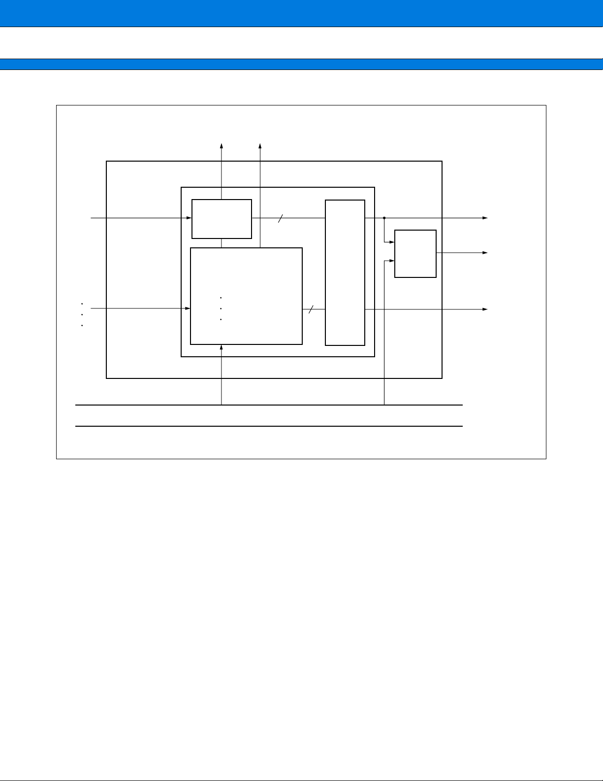
(3) Block diagram
MB91350A Series
RI00
UNMI WAKEUP
Determine order of priority
5
NMI
LEVEL determination
ICR00
VECTOR
determination
R-bus
("1" when LEVEL ≠ 11111B)
HLDREQ
Cancel
NMI
request
6
LEVEL,
VECTOR
Genera-
tion
LEVEL4 to LEVEL0
MHALTI
VCT5 to VCT0
61

MB91350A Series
2. External Interrupt/NMI Control
(1) Description
The external interrupt control unit is the block that controls external interrupt requests input to NMI
and INT0 to
INT15. The level that is detected as a request can be selected from “H”, “L”, rising edge, or falling edge (except
for NMI).
Note : The MB91F353A/353A/352A/351A does not have INT8 to INT15.
(2) Register list
External interrupt enable register (ENIR)
bit 7 bit 6 bit 5 bit 4 bit 3 bit 2 bit 1 bit 0
EN6EN7 EN5 EN4 EN3 EN2 EN1 EN0
External interrupt request register (EIRR)
bit 15 bit 14 bit 13 bit 12 bit 11 bit 10 bit 9 bit 8
ER6ER7 ER5 ER4 ER3 ER2 ER1 ER0
Request level setting register (ELVR)
bit 15 bit 14 bit 13 bit 12 bit 11 bit 10 bit 9 bit 8
LA7LB7 LB6 LA6 LB5 LA5 LB4 LA4
bit 7 bit 6 bit 5 bit 4 bit 3 bit 2 bit 1 bit 0
LA3LB3 LB2 LA2 LB1 LA1 LB0 LA0
The above registers (for 8 channels) are available in 2 sets; there are a total of 16 channels.
(3) Block diagram
R-bus
Interrupt
8
17
Interrupt enable register
Gate
Request F/F
Edge detection circuit
17
request
8
16
Interrupt source register
Interrupt level setting register
INT0 to INT15
NMI
62

MB91350A Series
3. REALOS-related Hardware
REALOS-related hardware is used by the real-time OS. Therefore, it cannot be used by user programs when
REALOS is used.
• Delay interrupt module
(1) Description
The delayed interrupt module generates a task switching interrupt.
This module enables software to issue or cancel an interrupt request to the CPU.
(2) Register list
Delayed Interrupt Control Register (DICR)
(3) Block diagram
Interrupt
request
bit 7 bit 6 bit 5
⎯⎯ ⎯⎯⎯⎯⎯DLYI
R-bus
bit 4
bit 3 bit 2 bit 1 bit 0
DLYI
63

MB91350A Series
• Bit Search Module
(1) Description
The bit search module searches data written to an input register for “0”, “1”, or a change point and returns the
detected bit position.
(2) Register list
bit 31 bit 0
0 detection data register (BSD0)
1 detection data register (BSD1)
Data register for transition detection (BSDC)
Detection result register (BSRR)
(3) Block diagram
D-bus
Address decoder
Input latch
Input detection
mode
Creating 1 detection data
Input bit search circuit
Search results
64

MB91350A Series
4. 8/16-bit Up/Down Counter
(1) Description
This block is the up/down counter/timer consisting of six event input pins, two 8-bit up/down counter, two 8-bit
reload/compare registers, and their control circuit.
The MB91F355A/F356B/F357B/355A/354A/V350A contains 2 channels of 8-bit up/down counter in this block.
The MB91F353A/353A/352A/351A contains 1 channel of 8-bit up/down counter in this block. It is not possible
to use in 16-bit mode.
This module has the following features.
• 8-bit count register enabling counting from (0)d to (255)d
(enabling counting from (0)d to (65535)d in 16 bits × 1 operation mode)
• Four different count modes available with selectable count clocks
Count mode Timer mode
Up/down count mode
Phase difference count mode (2 Multiplication)
Phase difference count mode (4 Multiplication)
• In timer mode, the ability to select the count clock input to use from among two internal clock circuits
Count clock
(When operating at
25 MHz)
• In up/down count mode, the ability to select the edge detection of the external pin input signals
Detection edge Falling edge detection
80 ns (12.5 MHz : Frequency division by 2)
320 ns (3.125 MHz : Frequency division by 8)
Rising edge detection
Detection at rising edge, falling edge, or both edges
Edge detection disabled
• The phase difference count mode is suitable for counting encoders such as motor encoders, and facilitates to
count the angle of revolution and number of revolutions to a high precision by inputting the A phase, B phase,
and Z phase outputs from the encoder
• ZIN pin has two selectable functions (valid in all modes)
ZIN pin Counter clear function
Gate function
• Compare and reload functions that can be used separately or in combination. When both functions are used
in combination, up/down counting can be performed at an arbitrary width.
Compare/reload
function
• Count direction flag used to identify the preceding count direction
• Capable of independently controlling the generation of interrupts for compare match, reload (underflow),
overflow, or on count direction change
Compare function (output interrupt request on compare match)
Compare function (output interrupt request and clear counter on compare
match)
Reload function (output interrupt request and reload on underflow)
Compare/reload function
(output interrupt request and clear counter on compare match; output interrupt
request and reload on underflow)
Compare/reload disabled
65

MB91350A Series
(2) Register list
• Up/down count register (UDCR)
Up/down count register ch.0 (UDCR0)
bit 7
bit 6 bit 5 bit 4 bit 3 bit 2 bit 1 bit 0
D06D07 D05 D04 D03 D02 D01 D00
Up/down count register ch.1 (UDCR1)
bit 15
*
bit 14 bit 13 bit 12 bit 11 bit 10 bit 9 bit 8
D14D15 D13 D12 D11 D10 D09 D08
• Reload compare register (RCR)
Reload compare register ch.0 (RCR0)
bit 7
Reload compare register ch.1 (RCR1)
bit 15
bit 6 bit 5 bit 4 bit 3 bit 2 bit 1 bit 0
D06D07 D05 D04 D03 D02 D01 D00
*
bit 14 bit 13 bit 12 bit 11 bit 10 bit 9 bit 8
D14D15 D13 D12 D11 D10 D09 D08
• Counter status register (CSR)
Counter status register ch.0, ch.1 (CSR0, CSR1*)
bit 7
bit 6 bit 5 bit 4 bit 3 bit 2 bit 1 bit 0
CITECSTR UDIE CMPF OVFF UDFF UDF1 UDF0
• Counter control register (CCRL)
Counter control register ch.0, ch.1 (CCRL0, CCRL1*)
bit 7
Reserved
bit 6 bit 5 bit 4 bit 3 bit 2 bit 1 bit 0
CTUT UCRE RLDE UDCC CGSC CGE1 CGE0
• Counter control register (CCRH)
Counter control register ch.0 (CCRH0)
bit 15
bit 14 bit 13 bit 12 bit 11 bit 10 bit 9 bit 8
CDCFM16E CFIE CLKS CMS1CMS0CES1CES0
• Counter control register ch.1 (CCRH1)*
bit 15
Reserved
bit 14 bit 13 bit 12 bit 11 bit 10 bit 9 bit 8
CDCF CFIE CLKS CMS1CMS0CES1CES0
* : Access to the UDCR1, RCR1, CSR1, CCRL1, CCRH1 registers is prohibited on the MB91F353A/353A/
352A/351A.
66

(3) Block diagram
• 8/16-bit up/down counter (ch.0)
MB91350A Series
Data bus
ZIN0
CGE1 CGE0 CGSC
Edge/level detection
Up/down
AIN0
BIN0
select
Prescaler
UDCC
CES1CES0
CMS0
CMS1
count
clock
Count
Clock
RCR0 (Reload
compare register ch.0)
CTUT
UCRE
Counter clear
Reload
control
RLDE
UDCR0 (up/down UDCR0
counter register ch.0)
CSTR
UDF1 UDF0 CDCF
M16E
UDFF OVFF
To ch.1
Carry
CMPF
UDIE
CITE
CLKS
CFIE
Interrupt output
67

MB91350A Series
•8/16-bit up/down counter (ch.1)
CGE1 CGE0 CGSC
Data bus
8 bits
RCR1 (Reload
compare register ch.1)
ZIN0, ZIN1
Edge/level detection
Up/down
AIN1
BIN1
Prescaler
CLKS
UDCC
CES1CES0
CMS1
count
clock
select
CMS0
Count
Clock
CTUT
Reload
control
UCRE
Counter clear
8 bits
RLDE
UDCR1 (up/down
counter register ch.1)
CSTR
UDF1 UDF0 CDCF
CMPF
UDFF OVFF
UDIE
CITE
CFIE
68
Interrupt output

MB91350A Series
5. 16-bit Reload Timer
(1) Description
The 16-bit timer consists of a 16-bit down counter, 16-bit reload register, internal clock, clock generation prescaler,
and control register.
The clock source can be selected from among three internal clocks (prepared by frequency dividing the machine
clock by 2/8/32, and also by 64/128 only for ch.3) and an external event.
The interrupt can be used to initiate a DMA transfer.
The MB91F353A/353A/352A/351A does not have timer outputs (TOT0 to TOT3).
This timer has 4 built-in channels.
(2) Register list
Control status register (TMCSR)
bit 15
bit 14 bit 13 bit 12 bit 11 bit 10 bit 9 bit 8
Reserved Reserved Reserved
⎯⎯ CSL2 CSL1 CSL0
(ch.3 only)
bit 7
Reserved
16-bit timer register (TMR)
bit 15
16-bit reload register (TMRLR)
bit 15
bit 6 bit 5 bit 4 bit 3 bit 2 bit 1 bit 0
⎯ OUTL RELD INTE UF CNTE TRG
bit 0
bit 0
69

MB91350A Series
(3) Block diagram
16
R-bus
16
7
16-bit reload register (TMRLR)
16-bit timer register (TMR) UF
Count enable
Clock selector
3
φ
φ2φ
35
1
2
2
Machine clock input
φ
φ
7
6
2
2
(ch.3 only)
CSL2
CSL1
CSL0
EXCK
Prescaler
clear
IN CTL.
Reload
OUT
CTL.
Re-trigger
RELD
OUTL
INTE
UF
CNTE
TRG
External timer output
(TOT0 to TOT3)
TOE0 to TOE3
IRQ
Note : The MB91F353A/353A/352A/351A does not have external timer outputs (TOT0 to TOT3).
70

MB91350A Series
6. PPG (Programmable Pulse Generator)
The PPG can efficiently output highly precise PWM wave forms.
The MB91F353A/353A/352A/351A contains 3 channels of PPG timer.
The MB91F355A/F356B/F357B/355A/354A/V350A contains 6 channels of PPG timer.
(1) Description
Each channel consists of a 16-bit down counter, 16-bit data register with cycle setting buffer, 16-bit compare
register with duty ratio setting buffer, and pin control unit.
The count clocks for the 16-bit down counter can be selected from the following 4 types : (peripheral clock φ,
φ/4, φ/16, φ/64)
The counter is initialized to "FFFF
PPG outputs (PPG0 to PPG5) are provided for each channel.
Note : The MB91F353A/353A/352A/351A contains 3 channels of PPG outputs PPG (0, 2, 4). There is no
PPG (1, 3, 5).
(2) Register list
H" at a reset or counter borrow.
General control register 10 (GCN10)
General control register 20 (GCN20)
Timer register (PTMR0 to PTMR5)
Cycle setting register (PCSR0 to PCSR5)
Duty setting register (PDUT0)
bit 15
bit 0
71

MB91350A Series
(3) Block diagram (overall configuration for 1 channel)
16-bit reload timer ch.0
TRG input
PPG timer ch.0
16-bit reload timer ch.1
General control
TRG input
PPG timer ch.1
register 10
(resource select)
General control
register 20
4
External TRG0 to
TRG3
External TRG4
TRG input
PPG timer ch.2
TRG input
PPG timer ch.3
TRG input
PPG timer ch.4
TRG input
External TRG5
PPG timer ch.5
Note : The MB91F353A/353A/352A/351A does not have PPG1, PPG3, PPG5 and external TRG5.
PPG0
PPG1
PPG2
PPG3
PPG4
PPG5
72

MB91350A Series
7. U-TIMER (16-bit timer for UART baud rate generation)
(1) Description
The U-TIMER is a 16-bit timer for generating the baud rate for the UART. An arbitrary baud rate can be set
depending on the combination of the chip operating frequency and U-TIMER reload value.
The MB91F353A/353A/352A/351A contains 4 channels of this timer.
The MB91F355A/F356B/F357B/355A/354A/V350A contains 5 channels of this timer.
(2) Register list
U-TIMER register (UTIM)
Reload register (UTIMR)
U-TIMER control register (UTIMC)
(3) Block diagram
bit 15
bit 15
φ
(Peripheral clock)
bit 15 bit 0
UTIMR (reload register)
load
UTIM (U-TIMER)
clock
bit 8 bit 7
bit 0
bit 0
underflow
control
f.f.
to UART
73

MB91350A Series
8. UART
(1) Description
The UART is a serial I/O port for asynchronous (start-stop) or CLK synchronous communication. This module
has the features listed below.
The MB91F353A/353A/352A/351A contains 4 channels of UART.
The MB91F355A/F356B/F357B/355A/354A/V350A contains 5 channels of UART.
• Full duplex double buffer
• Asynchronous (start-stop synchronized) or CLK synchronized transmission
• Supports multi-processor mode
• Completely programmable baud rate.
Arbitrary baud rate set by built-in timer (Refer to the section for "U-timer".)
• Variable baud rate can be input from an external clock.
• Error detection functions(parity, framing, overrun)
• Transmission signal format is NRZ
• UART (ch.0 to ch.2) can start DMA transfers using interrupts (ch.3 and ch.4 cannot start DMA transfers).
• Capable of clearing DMAC interrupt source by writing to DRCL register
(2) Register list
Serial input register/serial output register (SIDR/SODR)
bit 7
bit 6 bit 5 bit 4 bit 3 bit 2 bit 1 bit 0
D6D7 D5 D4 D3 D2 D1 D0
Serial status register (SSR)
bit 7
bit 6 bit 5 bit 4 bit 3 bit 2 bit 1 bit 0
OREPE FRE RDRF TDRE BDS RIE TIE
Serial mode register (SMR)
bit 7
bit 6 bit 5 bit 4 bit 3 bit 2 bit 1 bit 0
MD0MD1 ⎯⎯CS0 ⎯⎯⎯
Serial control register (SCR)
bit 7
bit 6 bit 5 bit 4 bit 3 bit 2 bit 1 bit 0
PPEN SBL CL A/D REC RXE TXE
DRCL register (DRCL)
bit 7
bit 6 bit 5 bit 4 bit 3 bit 2 bit 1 bit 0
⎯⎯⎯⎯⎯⎯⎯⎯
74

(3) Block diagram
Control
signal
MB91350A Series
RX interrupt
(to CPU)
From U-TIMER
External clock
SCK
SI (Receive data)
Receive status
decision circuit
Clock
selection
circuit
Reception
clock
Reception control
detection circuit
Received bit
Received parity
RX shifter
circuit
Start bit
Counter
Counter
complete
Transmission clock
RX
SCK (clock)
TX interrupt
(to CPU)
Transmission
control circuit
Transmission
start
Transmission bit
Counter
Transmission
parity Counter
SO (Send data)
TX shifter
Start trans-
mission
SMR
Register
For DMA
received error generating
signal (to DMAC)
MD1
MD0
SCR
CS0
Register
SIDR SODR
R - bus
PEN
P
SBL
CL
A/D
REC
RXE
TXE
SSR
Register
PE
ORE
FRE
RDRF
TDRE
BDS
RIE
TIE
Control signal
75

MB91350A Series
9. Extended I/O serial interface (SIO)
(1) Description
This block is an 8-bit × 1 channel serial I/O interface that allows data transfer using clock synchronization.
LSB-first or MSB-first transfer mode can be selected for data transfer.
The MB91F353A/353A/352A/351A contains 2 channels of this SIO.
The MB91F355A/F356B/F357B/355A/354A/V350A contains 3 channels of this SIO.
The serial I/O interface operates in 2 modes :
• Internal shift clock mode : Data is transferred synchronized with the internal clock.
• External shift clock mode : Data is transferred synchronized with a clock supplied via the external pin (SCK).
In this mode, data can also be transferred using CPU instructions by operating the
general-purpose port that shares the external pin (SCK) .
(2) Register list
Serial mode control status register (SMCS)
bit 15
bit 14 bit 13 bit 12 bit 11 bit 10 bit 9 bit 8
SMD1SMD2 SMD0 SIE SIR BUSY STOP STRT
bit 7
bit 6 bit 5 bit 4 bit 3 bit 2 bit 1 bit 0
⎯⎯⎯⎯MODE BDS ⎯⎯
SIO test register (SES)
bit 15
bit 14 bit 13 bit 12 bit 11 bit 10 bit 9 bit 8
⎯⎯⎯⎯⎯⎯TST1 TST0
SDR (Serial Data Register) (SDR)
bit 7
bit 6 bit 5 bit 4 bit 3 bit 2 bit 1 bit 0
D6D7 D5 D4 D3 D2 D1 D0
SIO prescaler control register (CDCR)
bit 15
bit 14 bit 13 bit 12 bit 11 bit 10 bit 9 bit 8
⎯MD ⎯⎯DIV3 DIV2 DIV1 DIV0
DMAC interrupt source clear register (SRCL)
bit 7
bit 6 bit 5 bit 4 bit 3 bit 2 bit 1 bit 0
⎯⎯⎯⎯⎯⎯⎯⎯
76

(3) Block diagram
MB91350A Series
Internal data bus
(MSB first) D0 to D7 (LSB first) D0 to D7
Select transmitting direction
SI6, SI7
SDR (Serial Data Register)
SO6, SO7
SCK6, SCK7
Control circuit
Internal clock
21 0
SMD2 SMD1 SMD0 SIE SIR BUSY STOP STRT MODE BDS
Interrupt
request
Internal data bus
Initial Value
Read
Write
Shift clock counter
SCE
PFR
Register
77

MB91350A Series
10. 16-bit free-run timer
(1) Description
The 16-bit free-run timer consists of a 16-bit up counter, control register, and status register. The count values
of this timer are used as the base timer for the output compare and input capture modules.
• Four count clock frequencies are available.
• An interrupt can be generated on counter overflow.
• The counter can be initialized upon a match with compare register 0 of the output compare unit, depending
on the mode.
(2) Register list
Timer data register (upper) (TCDT)
bit 15
Timer data register (lower) (TCDT)
bit 7
bit 14 bit 13 bit 12 bit 11 bit 10 bit 9 bit 8
T14T15 T13 T12 T11 T10 T9 T8
bit 6 bit 5 bit 4 bit 3 bit 2 bit 1 bit 0
T06T07 T05 T04 T03 T02 T01 T00
Timer control status register (lower) (TCCS)
bit 7
bit 6 bit 5 bit 4 bit 3 bit 2 bit 1 bit 0
IVFECLK IVFE STOP MODE CLR CLK1 CLK0
(3) Block diagram
ECLK IVF IVFE STOP MODE CLR CLK1 CLK0
R-bus
Timer data register
(TCDT)
Interrupt
Clock
Divider
Clock
select
φ
FRCK
78
To internal circuit (T15 to T00)
Comparator

MB91350A Series
11. Input Capture
(1) Description
This module detects the rising or falling edge or both edges of an external input signal and then, stores the value
of the 16-bit free-run timer in a register. In addition, the module can generate an interrupt upon detection of an
edge.
The input capture module consists of input capture data registers and a control register.
Each input capture unit has a corresponding external input pin.
• The detection edge of the external input can be selected from among 3 types.
Rising edge
Falling edge
Both edges
• An interrupt can be generated upon detection of a valid edge in the external input.
(2) Register list
Input capture data register (upper) (IPCP)
bit 15
bit 14 bit 13 bit 12 bit 11 bit 10 bit 9 bit 8
CP14CP15 CP13 CP12 CP11 CP10 CP09 CP08
Input capture data register (lower) (IPCP)
bit 7
bit 6 bit 5 bit 4 bit 3 bit 2 bit 1 bit 0
CP06CP07 CP05 CP04 CP03 CP02 CP01 CP00
Input capture control register (ICS23)
bit 7
bit 6 bit 5 bit 4 bit 3 bit 2 bit 1 bit 0
ICP2ICP3 ICE3 ICE2 EG31 EG30 EG21 EG20
Input capture control register (ICS01)
bit 7
bit 6 bit 5 bit 4 bit 3 bit 2 bit 1 bit 0
ICP0ICP1 ICE1 ICE0 EG11 EG10 EG01 EG00
79

MB91350A Series
(3) Block diagram
16-bit timer counter value
(T15 to T00)
Input capture data register
ch.0, ch.2
16-bit timer counter value
R-bus
(T15 to T00)
Input capture data register
ch.1, ch.3
Edge
detection
EG11 EG10 EG01 EG00
EG31 EG30 EG21 EG20
Edge
detection
ICP1 ICP0 ICE1 ICE0
ICP3 ICP2 ICE3 ICE2
IN0, IN2
Input pin
IN1, IN3
Input pin
Interrupt
Interrupt
80

MB91350A Series
12. Output Compare
(1) Description
The output compare module consists of a 16-bit compare register, compare output latch, and control register.
When the 16-bit free-run timer value matches the compare register value, the output level is inverted and an
interrupt is issued.
The MB91F353A/353A/352A/351A contains 2 channels of this block.
The MB91F355A/F356B/F357B/355A/354A/V350A contains 8 channels of this block.
This module has the following features.
• The output compare is able to operate independent of each of 8 compare register. There are output pins and
interrupt flags corresponding to each of the compare registers.
• A pair of compare registers can be used to control the output terminal.
The output terminal is reversed by using two compare registers.
• Capable of setting the initial value for each output pin.
• Interrupts can be generated upon a compare match.
• The ch.0 compare register is used as the compare clear register for the 16-bit free-run timer.
(2) Register list
Compare register (OCCP)
bit 15
Compare register (OCCP)
bit 7
Output control register (OCS01)
bit 15 bit 14 bit 13 bit 12 bit 11 bit 10 bit 9 bit 8
Output control register (OCS23)
bit 7 bit 6 bit 5 bit 4 bit 3 bit 2 bit 1 bit 0
bit 14 bit 13 bit 12 bit 11 bit 10 bit 9 bit 8
C14C15 C13 C12 C11 C10 C09 C08
bit 6 bit 5 bit 4 bit 3 bit 2 bit 1 bit 0
C06C07 C05 C04 C03 C02 C01 C00
⎯⎯⎯CMOD ⎯⎯OTD1 OTD0
ICP0ICP1 ICE1 ICE0 ⎯⎯CST1 CST0
81

MB91350A Series
(3) Block diagram
(Only ch.0 is used as a free-run timer
clear register.)
Output compare
register
Compare circuit
Output compare
register
R-bus
Compare circuit
CST1 CST0
16-bit free-run timer
OTD1 OTD0
Compare
output latch
CMOD
Compare
output latch
ICP1 ICP0 ICE1 ICE0
OTE0, OTE2,
OTE4, OTE6
Output
(ch.0, ch.2, ch.4, ch.6)
OTE0 and OTE7 exist in PFR0.
OTE1, OTE3,
OTE5, OTE7
Output
(ch.1, ch.3, ch.5, ch.7)
Interrupt output
Interrupt output
82

13. I2C Interface
(1) Description
2
C interface is a serial I/O port supporting the Inter-IC bus, operating as a master/slave device on the I2C
The I
bus. It has the following features :
• Master/slave transmission and reception
• Arbitration function
• Clock sync function
• Slave address and general call address detection function
• Transmission direction detection function
• Repeated start condition generation and detection function
• Bus error detection function
• 10-bit/7-bit slave address
• Slave address receive acknowledge control when in master mode
• Support for composite slave addresses
• Capable of interrupt when a transmission or bus error occurs
• Standard mode (Max 100 kbps)/High speed mode (Max 400 kbps) supported
MB91350A Series
83

MB91350A Series
(2) Register list
Bus control register (IBCR)
bit 15 bit 14 bit 13 bit 12 bit 11 bit 10 bit 9 bit 8
Bus status register (IBSR)
bit 7 bit 6 bit 5 bit 4 bit 3 bit 2 bit 1 bit 0
10-bit slave address resister (ITBA)
bit 15 bit 14 bit 13 bit 12 bit 11 bit 10 bit 9 bit 8
bit 7 bit 6 bit 5 bit 4 bit 3 bit 2 bit 1 bit 0
10-bit slave address mask resister (ITMK)
bit 15 bit 14 bit 13 bit 12 bit 11 bit 10 bit 9 bit 8
BEIEBER SCC MSS ACK GCAA INTE INT
RSCBB AL LRB TRX AAS GCA ADT
⎯⎯⎯⎯⎯⎯TA9 TA8
TA6TA7 TA5 TA4 TA3 TA2 TA1 TA0
RALENTB ⎯⎯⎯⎯TM9 TM8
bit 7 bit 6 bit 5 bit 4 bit 3 bit 2 bit 1 bit 0
7-bit slave address resister (ISBA)
bit 7 bit 6 bit 5 bit 4 bit 3 bit 2 bit 1 bit 0
7-bit slave address mask resister (ISMK)
bit 15 bit 14 bit 13 bit 12 bit 11 bit 10 bit 9 bit 8
D/A data register (IDAR)
bit 7 bit 6 bit 5 bit 4 bit 3 bit 2 bit 1 bit 0
Clock control register (ICCR)
bit 15 bit 14 bit 13 bit 12 bit 11 bit 10 bit 9 bit 8
Clock disable register (IDBL)
bit 7 bit 6 bit 5 bit 4 bit 3 bit 2 bit 1 bit 0
TM6TM7 TM5 TM4 TM3 TM2 TM1 TM0
SA6⎯ SA5 SA4 SA3 SA2 SA1 SA0
SM6ENSB SM5 SM4 SM3 SM2 SM1 SM0
D6D7 D5 D4 D3 D2 D1 D0
⎯TEST EN CS4 CS3 CS2
⎯⎯⎯⎯⎯⎯⎯DBL
CS1
CS0
84

(3) Block diagram
ICCR
EN
IDBL
DBL
ICCR
CS4
CS3
CS2
CS1
CS0
IBSR
BB
RSC
LRB
TRX
ADT
I2C operation enable
Clock enable
Clock divide 2
2 3 45 32
Clock selector 2 (1/12)
Bus busy
Start
Last Bit
Sending/
receiving
MB91350A Series
CLKP
Sync
Shift clock generation
Shift clock edge
changing timing
Start stop condition
detection
Error
First byte
R- bus
AL
IBCR
BER
BEIE
INTE
INT
IBCR
SCC
MSS
ACK
GCAA
IBSR
AAS
GCA
ISMK
ENSB
ITMK
ENTB RAL
ACK enable
GC-ACK enable
Start
Master
Slave
Global call
Arbitration lost detection
Interrupt request
End
Start stop condition
generation
IDAR
Slave address
compare
IRQ
SCL
SDA
ITBA ITMK ISBA ISMK
85

MB91350A Series
14. A/D converter
(1) Description
The A/D converter converts the analog input voltage into a digital value. It has the following features :
• Conversion time : 1.48 µs minimum per channel
• Employing serial / parallel conversion type for sample and hold circuit.
• 10-bit resolution (switchable between 8 and 10 bits)
• Programmatic selection of the analog input from among 12 channels
(The MB91F353A/353A/352A/351A are input 8 channels.)
• Conversion mode
Single conversion mode : Converts 1 selected channel a single time.
Scan conversion mode : Scanning conversion of up to 4 channels.
• Converted data is stored in a data buffer (a total of 4 data buffers) .
• An interrupt request to the CPU can be generated upon completion of A/D conversion. The interrupt can be
used to start a DMA transfer.
• The startup source can be selected from among software, external trigger (falling edge), and reload timer ch.2
(rising edge).
(2) Register list
Control status register (ADCS2/ADCS1)
Conversion time setting register (ADCT)
Converted data register 0 (ADTH0/ADTL0)
Converted data register 1 (ADTH1/ADTL1)
Converted data register 2 (ADTH2/ADTL2)
Converted data register 3 (ADTH3/ADTL3)
bit 15 bit 0
ADTH2
bit 8 bit 7
ADCS1ADCS2
ADTL0ADTH0
ADTL1ADTH1
ADTL2
ADTL3ADTH3
86

(3) Block diagram
Analog input
AN0
AN1
AN2
AN3
AN4
AN5
AN6
AN7
AN8
AN9
AN10
AN11
MB91350A Series
AVCC, AVRH, AVSS/AVRL
M
P
X
S/H
10-bit
A/D
Convertor
ADT0
M
ADT1
P
ADT2
X
ADT3
R-bus
Control logic
16-bit reload timer ch.2
External input
Note : The MB91F353A/353A/352A/351A does not have inputs AN8 to AN11.
Interrupt
87
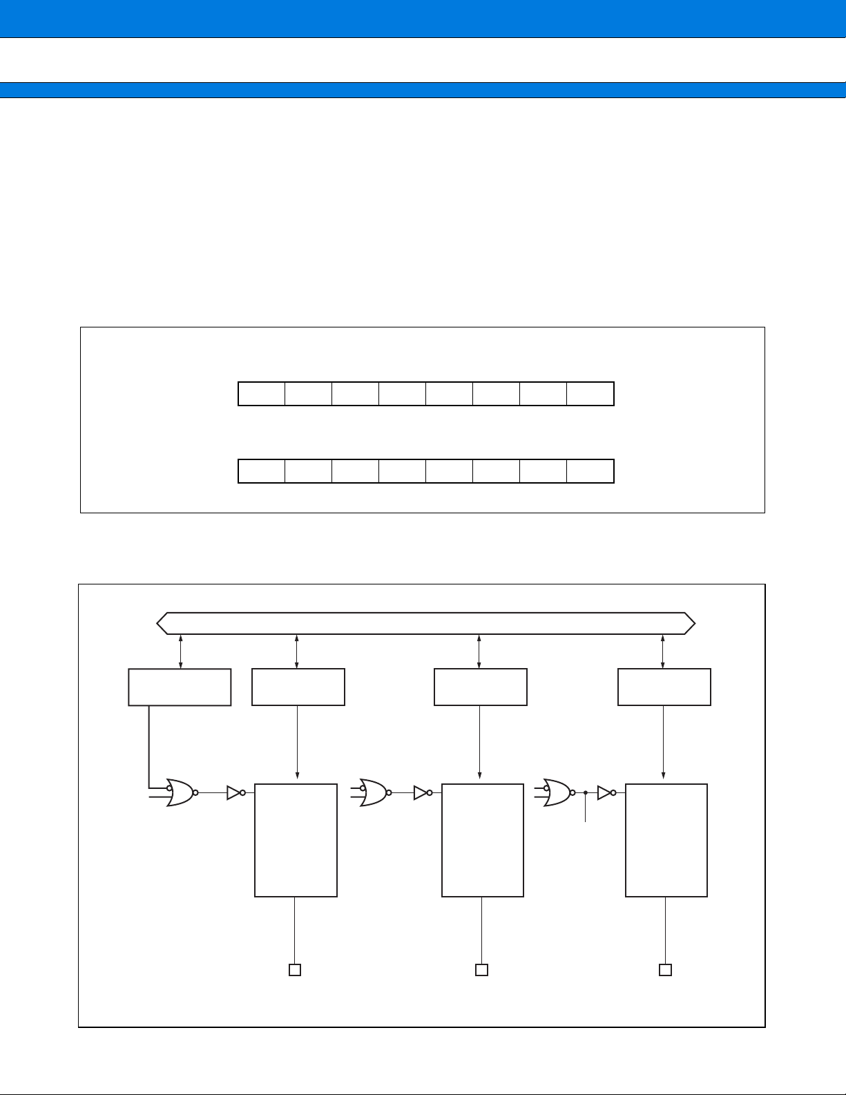
MB91350A Series
15. 8-bit D/A converter
(1) Description
This block contains 3 channels of 8-bit D/A converters and D/A converter registers that can be used to control
the independent output of each channel. The block has the following features.
• Power saving function
• 3.3 V interface
Note : The MB91F353A/353A/352A/351A contains 2 channels of D/A converter.
(2) Register list
D/A data register 0 to 2 (DADR0 to DADR2)
bit 7 bit 6 bit 5 bit 4 bit 3 bit 2 bit 1 bit 0
DA6DA7 DA5 DA4 DA3 DA2 DA1 DA0
D/A control register 0 to 2 (DACR0 to DACR2)
bit 7 bit 6 bit 5 bit 4 bit 3 bit 2 bit 1 bit 0
⎯⎯⎯⎯⎯⎯⎯DAE
Note : The MB91F353A/353A/352A/351A does not have DADR2, DACR2.
(3) Block diagram
R-bus
D/A control
DAE0
STOP STOP
D/A D/A
DAE1
PD
D/A
converter
PD
D/A
converter
D/A
DAE2
PD
STOP
D/A
converter
88
D/A output 0 D/A output 1
D/A output 2

MB91350A Series
16. DMAC (DMA Controller)
(1) Description
This module provides direct memory access (DMA) transfers in the FR family devices.
The DMAC enables high speed transfers for various data without CPU intervention, thereby improving system
performance.
• Hardware configuration
The main components of this module are as follows :
• Independent DMA channels × 5 channels
• 5 channels independent access control circuits
• 32-bit address registers (Supports reloading : 2 per channel)
• 16-bit transfer count registers (Supports reloading : 1 per channel)
• 4-bit block count registers (1 per channel)
• External transfer request input pins : DREQ0, DREQ1, and DREQ2. For ch.0 to ch.2 only
Note : The MB91F353A/353A/352A/351A do not have an external interface.
• External transfer request acceptance output pins : DACK0, DACK1, and DACK2. For ch.0 to ch.2 only
Note : The MB91F353A/353A/352A/351A do not have an external interface.
• DMA end output pins : DEOP0, DEOP1, and DEOP2. For ch.0 to ch.2 only
Note : The MB91F353A/353A/352A/351A do not have an external interface.
• Fly-by transfer (memory to I/O and I/O to memory). For ch.0 to ch.2 only
Note : The MB91F353A/353A/352A/351A do not support fly-by transfer.
• 2-cycle transfer
• Main functions
This module has the following major functions for data transfer :
• Supports data transfer over multiple independent channels (5 channels)
(1) Priority order (ch.0
(2) Order can be reversed for ch.0 and ch.1
(3) DMAC activation triggers
• External dedicated pin input (edge detection/level detection for ch.0 to ch.2 only)
Note : The MB91F353A/353A/352A/351A do not have an external interface.
• Internal peripheral request (Interrupt request sharing, including external interrupts)
• Software request (register write)
(4)Transmission mode
• Demand transfer, burst transfer, step transfer, or block transfer
• Addressing mode : 32-bit full addressing (increment, decrement, or fixed)
(address increment can be in the range - 255 to + 255)
• Data length : Byte, halfword, or word
• Single-shot or reload operation selectable
> ch.1 > ch.2 > ch.3 > ch.4)
89

MB91350A Series
(2) Register Description
ch.0 Control/status Register A
Register B
ch.1 Control/status Register A
Register B
ch.2 Control/status Register A
Register B
ch.3 Control/status Register A
Register B
ch.4 Control/status Register A
Register B
Overall control register
bit 31 bit 0
(DMACA0)
(DMACB0)
(DMACA1)
(DMACB1)
(DMACA2)
(DMACB2)
(DMACA3)
(DMACB3)
(DMACA4)
(DMACB4)
(DMACR)
ch.0 Transfer source address register
ch.1 Transfer source address register
ch.2 Transfer source address register
ch.3 Transfer source address register
ch.4 Transfer source address register
(DMASA0)
(DMADA0)
(DMASA1)
(DMADA1)
(DMASA2)
(DMADA2)
(DMASA3)
(DMADA3)
(DMASA4)
(DMADA4)
90

(3) Block diagram
MB91350A Series
To bus
control-
ler
DMA transfer request
to bus controller
Read
Write
Read/write
control
DDNO
Bus control block
Access
Counter buffer
Counter
Buffer
Selector
DTC two-stage register
Counter
Buffer
Selector
BLK register
DDNO register
Selector
DSAD two-stage register
Write back
back
Write
DTCR
Priority circuit
transition
DMA control
DMA start
source select
circuit &
request
acceptance
control
State
circuit
SADM, SASZ [7:0] SADR
Peripheral start request/
Stop input
External pin start request/
Stop input
DSS [3:0]
To interrupt controller
ERIR, EDIR
peripheral interrupt
Clear
TYPE, MOD, WS
IRQ [4:0]
MCLREQ
X-bus
Bus control block
address
Address counter
Write back
Counter buffer
DDAD two-stage register
Selector Selector
DADM, DASZ [7:0] DADR
5-channel DMAC block diagram
91

MB91350A Series
■ ELECTRICAL CHARACTERISTICS
1. Absolute Maximum Rating
Parameter Symbol
Min Max
Power supply voltage*
Analog power supply voltage*
Analog power supply voltage*
Analog reference voltage*
Input voltage*
1
Input voltage (N-ch open-drain) *
Analog pin input voltage*
Output voltage*
Maximum clamp current I
Total maximum clamp current Σ|I
“L” level maximum output current I
“L” level maximum output current
(N-ch open-drain)
“L” level average output current I
“L” level average output current
(N-ch open-drain)
“L” level total maximum output current ΣI
“L” level total average output current ΣI
“H” level maximum output current I
“H” level average output current I
“H” level total maximum output current ΣI
“H” level total average output current ΣI
Power consumption P
1
1
1
1
VCC VSS − 0.5 VSS + 4.0 V *2
DAVC VSS − 0.5 VSS + 4.0 V *3
AVCC VSS − 0.5 VSS + 4.0 V *3
AVRH VSS − 0.5 VSS + 4.0 V *3
VI VSS − 0.5 VCC + 0.5 V *8
1
1
1
VIND VSS − 0.5 VSS + 5.5 V
VIA VSS − 0.5 AVCC + 0.5 V *8
VO VSS − 0.5 VCC + 0.5 V
CLAMP − 2.0 + 2.0 mA *7
CLAMP| ⎯ 20 mA *7
OL ⎯ 10 mA *4
OLND ⎯ 20 mA
I
OLAV ⎯ 8mA*5
I
OLAVND ⎯ 15 mA
OL ⎯ 100 mA
OLAV ⎯ 50 mA *6
OH ⎯ − 10 mA *4
OHAV ⎯ − 4mA*5
OH ⎯ − 50 mA
OHAV ⎯ − 20 mA *6
D ⎯ 850 mW
Operating temperature Ta − 40 + 85 °C
Storage temperature T
STG ⎯ + 125 °C
Rating
Unit Remarks
*1 : The parameter is based on VSS = DAVS = AVSS = 0 V.
*2 : V
CC must not be lower than VSS − 0.3 V.
*3 : Be careful not to exceed "V
CC + 0.3 V" , for example, when the power is turned on.
*4 : The maximum output current is the peak value for a single pin.
*5 : The average output current is the average current for a single pin over a period of 100 ms.
*6 : The total average output current is the average current for all pins over a period of 100 ms.
92
(Continued)

MB91350A Series
(Continued)
*7 : • Relevant pins : Ports 2, 3, 4, 5, 6, 8, 9, A, H, I, K, M, N, O and AN (A/D input) : MB91F353A/353A/352A/351A
Ports 2, 3, 4, 5, 6, 8, 9, A, B, C, G, H, I, J, K, M, N, O, P and AN (A/D input) :
MB91F355A/F356B/F357B/355A/354A
• Use within recommended operating conditions.
• Use at DC voltage (current).
• + B signals are input signals that exceed the V
• A limiting resistance should always be applied to +B signals by connecting the resistance between the +B
signal and the microcontroller.
• The value of the limiting resistance should be set so that when the + B signal is applied the input current to
the microcontroller pin does not exceed rated values, either instantaneously or for prolonged periods.
• Note that when the microcontroller drive current is low, such as in low power consumption mode, the + B
input potential can increase the potential at the V
devices.
• Note that if a + B input is applied when the microcontroller is off (not fixed at 0 V), power is supplied
through the pin, possibly causing the microcontroller to partially operate.
• Note that if a + B input is applied when the power supply is turned on, power is supplied through the pin,
possibly resulting in a power-supply voltage at which power-on reset does not work.
• Ensure that a + B input pin does not form an open circuit.
• Note that analog I/O pins other than the A/D input pins (such as the LCD drive and comparator input pins)
cannot input + B.
• Sample recommended circuits :
CC voltage.
CC pin via a protective diode, possibly affecting other
• Input/output equivalent circuits
Protective diode
Vcc
Limiting
P-ch
resistance
+ B input (0 V to 16 V)
N-ch
R
I must not exceed the rated voltage. However, If the maximum current to/from an input is limited by some
*8 : V
means using external components, the I
CLAMP rating supersedes the VI rating.
WARNING: Semiconductor devices can be permanently damaged by application of stress (voltage, current,
temperature, etc.) in excess of absolute maximum ratings. Do not exceed these ratings.
93

MB91350A Series
2. Recommended Operating Conditions
( Other than MB91F356B/F357B)
Parameter Symbol
V
Power supply voltage
CC 3.0 3.6 V During normal operation
V
CC 3.0 3.6 V Hold RAM status at stop
Val ue
Min Max
(V
SS = DAVS = AVSS = 0 V)
Unit Remarks
DAVC V
SS − 0.3 VSS + 3.6
Analog power supply voltage
AVCC VSS − 0.3 VSS + 3.6
Analog reference voltage AVRH AV
SS AVCC V
Operating temperature Ta − 40 + 85 °C
(MB91F356B/F357B only)
Val ue
Parameter Symbol
Unit Remarks
Min Max
CC 2.7 3.6 V During normal operation
V
V
Power supply voltage
CC 2.7 3.6 V Hold RAM status at stop
V
CC 3.0 3.6 V
DAVC V
SS − 0.3 VSS + 3.6
Analog power supply voltage
AV
CC VSS − 0.3 VSS + 3.6
Analog reference voltage AVRH AV
SS AVCC V
− 40 + 85 °C
Operating temperature Ta
0 +70 °C
V
(V
SS = DAVS = AVSS = 0 V)
When writing or erasing
Flash memory
V
When writing or erasing
Flash memory*
* : Including the F355A/F353A
WARNING: The recommended operating conditions are required in order to ensure the normal operation of the
semiconductor device. All of the device’s electrical characteristics are warranted when the device is
operated within these ranges.
Always use semiconductor devices within their recommended operating condition ranges. Operation
outside these ranges may adversely affect reliability and could result in device failure.
No warranty is made with respect to uses, operating conditions, or combinations not represented on
the data sheet. Users considering application outside the listed conditions are advised to contact their
FUJITSU representatives beforehand.
94

MB91350A Series
3. DC Characteristics
(VCC = 3.0 V to 3.6 V, VCC = 2.7 V to 3.6 V (MB91F356B/F357B only) , VSS = DAVS = AVSS = 0 V, Ta = − 40 °C to + 85 °C)
Parameter
“H” level
input voltage
“L” level
input voltage
Symbol
V
IH
VIHS
VIHST
IL
V
VILS
VILST
Pin name
Port 2, 3, 4, 5, 6,
9, A
Port 2, 3, 4, 5, 6,
9, A, B, C
Port 8, H, I, M,
N, O, MD0,
MD1, MD2,
INIT
, NMI
Port 8, G, H, I,
M, N, O, P,
MD0, MD1,
MD2, INIT
, NMI
Port K, L
Port J, K, L
Port 2, 3, 4, 5, 6,
9, A
Port 2, 3, 4, 5, 6,
9, A, B, C
Port 8, H, I, M,
N, O, MD0,
MD1, MD2,
INIT
, NMI
Port 8, G, H, I,
M, N, O, P,
MD0, MD1,
MD2, INIT
, NMI
Port K, L
Port J, K, L
Conditions
⎯
⎯ V
Min Typ Max
V
CC ×
0.65
VCC × 0.8
SS ⎯
Val ue
⎯
V
CC + 0.3
5.25
CC × 0.25
V
VCC × 0.2
Unit Remarks
MB91F353A/353A/
352A/351A
MB91F355A/F356B/
F357B/355A/354A
Hysteresis input
MB91F353A/353A/
352A/351A
Hysteresis input
V
MB91F355A/F356B/
F357B/355A/354A
Hysteresis input withstand voltage of 5 V
MB91F353A/353A/
352A/351A
Hysteresis input withstand voltage of 5 V
MB91F355A/F356B/
F357B/355A/354A
MB91F353A/353A/
352A/351A
MB91F355A/F356B/
F357B/355A/354A
Hysteresis input
MB91F353A/353A/
352A/351A
Hysteresis input
V
MB91F355A/F356B/
F357B/355A/354A
Hysteresis input withstand voltage of 5 V
MB91F353A/353A/
352A/351A
Hysteresis input withstand voltage of 5 V
MB91F355A/F356B/
F357B/355A/354A
(Continued)
95

MB91350A Series
CC = 3.0 V to 3.6 V, VCC = 2.7 V to 3.6 V (MB91F356B/F357B only) , VSS = DAVS = AVSS = 0 V, Ta = − 40 °C to + 85 °C)
(V
Parameter
“H” level
output
voltage
“L” level
output
voltage
Symbol
V
OH
V
OL1
Pin name Conditions
Port 2, 3, 4,
5, 6, 8, 9, A,
H, I, J, K, M,
N, O
CC = 3.0 V,
Port 2, 3, 4,
V
I
OH = −4.0 mA
5, 6, 8, 9, A,
B, C, G, H,
I, J, K, M, N,
O, P
Port 2, 3, 4,
5, 6, 8, 9, A,
H, I, K, M,
N, O
CC = 3.0 V,
Port 2, 3, 4,
V
I
OL = 4.0 mA
5, 6, 8, 9, A,
B, C, G, H,
I, J, K, M, N,
O, P
Min Typ Max
VCC − 0.5 ⎯ VCC V
V
SS ⎯ 0.4 V
Val ue
Unit Remarks
MB91F353A/
353A/352A/351A
MB91F355A/
F356B/F357B/
355A/354A
MB91F353A/
353A/352A/351A
MB91F355A/
F356B/F357B/
355A/354A
Input leak
current
(High-Z
Output
Leakage
Current)
Pull-up
resistance
Power
supply
current
V
OL2 Port L
I
LI All input pin
Setting pin
R
UP
INIT
Pull Up
CC VCC
I
,
VCC = 3.0 V,
I
OL = 15.0 mA
VCC = 3.6 V,
0
<VI <VCC
VCC = 3.6 V,
V
I = 0.45 V
fC =
12.5 MHz,
V
CC =
3.3 V
Flash
MASK
Flash
MASK
− 5 ⎯ + 5 µA
25 50 200 kΩ
160 220
125 150
⎯
mA
85 100
75 90
N-ch
open-drain
MB91F353A/
353A/352A/351A
Multiply by 4RUN
When operating
at
CLKB : 50 MHz
CLKT : 25 MHz
CLKP : 25 MHz
MB91F353A/
353A/352A/351A
Multiply by 2RUN
When operating
at
CLKB : 25 MHz
CLKT : 25 MHz
CLKP : 12.5 MHz
96
(Continued)

MB91350A Series
(Continued)
CC = 3.0 V to 3.6 V, VCC = 2.7 V to 3.6 V (MB91F356B/F357B only) , VSS = DAVS = AVSS = 0 V, Ta = − 40 °C to + 85 °C)
(V
Parameter
Power
supply
current
Symbol
Pin name Conditions
Min Typ Max
CC
I
fC = 12.5 MHz,
V
CC = 3.3 V
I
CCS 100 140
VCC
⎯
Val ue
160 220
Unit Remarks
MB91F355A/
F356B/F357B/
355A/354A
Multiply by 4RUN
When operating at
CLKB : 50 MHz
CLKT : 25 MHz
CLKP : 25 MHz
MB91F353A/
353A/352A/351A
mA
Multiply by 4RUN
When operating at
CLKB : 50 MHz
CLKT : 25 MHz
CLKP : 25 MHz
MB91F355A/
F356B/F357B/
355A/354A
Sleep
CLKP : When operating at 25 MHz
Input
capacitance
I
I
CCH
CCL
Ta = + 25 °C,
V
CC = 3.3 V
1 100 µAAt stop
0.3 3.0
Ta = + 25 °C,
f
C = 32.768 kHz,
V
ICCLS 0.2 2.0
I
CCT 5 120 µA
CC = 3.3 V
Other than
V
CC, VSS,
C
AV
IH
CC, AVSS,
⎯⎯515pF
DAVC,
DAVS
Sub RUN
When operating at
CLKB : 32.768 kHz
CLKT : 32.768 kHz
mA
CLKP : 32.768 kHz
Sub-sleep
When operating at
CLKP : 32.768 kHz
When operating in
watch mode
(Main Off, STOP)
97

MB91350A Series
4. AC Characteristics
(1) Clock Timing
Parameter
Symbol
Pin
name
(V
CC = 3.0 V to 3.6 V, VCC = 2.7 V to 3.6 V (MB91F356B/F357B only) ,
V
SS = DAVS = AVSS = 0 V, Ta = − 40 °C to + 85 °C)
Value
Conditions
Unit Remarks
Min Typ Max
Clock
frequency
Clock cycle time t
Clock
frequency
Internal operating
clock frequency
Internal operating
clock cycle time
Clock
frequency
Clock cycle time t
Input clock pulse
width
Internal operating
clock frequency
Internal operating
clock cycle time
f
C
10
12.5 MHz
MAIN PLL
(When operating at max
internal frequency
X0,
C 80 100 ns
X1
⎯
(50 MHz) = 12.5 MHz
self-oscillation with ×
4 PLL)
C 10 25 MHz
f
⎯
fCP
f
CPP
CPT External bus
f
tCP 20
t
CPP
CPT External bus
t
fC
C 28.6 30.51 33.3 µs
⎯
f
CP,
f
CPP,
f
CPT
t
CP,
t
CPP,
t
CPT
When a minimum
value of 12.5 MHz is
input as the X0 clock
⎯
frequency and x4
multiplication is set
for the PLL of the
oscillator circuit
X0A,
X1A
X0,
X1
When a standard
value of 32.768 kHz is
⎯
input as the X0A
clock frequency
⎯
P
WH/tC
PWL/tC
2.94*
40
30 32.768 35 kHz
40
2* 32.768 kHz
⎯
30.51 500* µs
50
25
340* ns
60 %
MAIN self-oscillation
(frequency-halved input)
CPU
MHz
Peripheral
CPU
Peripheral
SUB self-oscillation
* : The values assume a gear cycle of 1/16.
• Conditions for measuring the clock timing ratings
t
C
P
WH
98
0.8 V
CC
0.2 V
CC
P
WL
Output pin
C = 50 pF

• Operation Guaranteed Range (Other than MB91F356B/F357B)
CC (V)
V
Operation Guaranteed Range (Ta = − 40 °C to + 85 °C)
f
CPP is represented by the shaded area.
3.6
3.0
Power supply
0
50252.94
Internal clock
• External/internal clock setting range
fCP, fCPP
(MHz)
MB91350A Series
(MHz)
50
CP
f
Oscillation input clock f
C = 12.5 MHz
CPU (CLKB) :
Peripheral (CLKP)
Internal clock
fCPP,
f
CPT
25
12.5
External bus (CLKT) :
CPU : Peripheral division
4 : 4 2 : 2 1 : 2
ratios
CPU : Peripheral division ratio
Notes : • When the PLL is used, the external clock input must fall between 10.0 MHz and 12.5 MHz.
• Set the PLL oscillation stabilization wait time longer than 454.5 µs.
• The internal clock gear setting should not exceed the relevant value in the table in “(1) Clock timing ratings”.
99

MB91350A Series
• Operation Guaranteed Range (MB91F356B/F357B only)
For Flash memory wait of 2 (FLWC register : WTC[2 : 0] = 010)
VCC (V)
Operation Guaranteed Range (Ta = − 40 °C to + 85 °C)
f
3.6
3.0
2.8
Power supply
2.7
05025 33 402.94
Internal clock
CPP is represented by the shaded area.
fCP, fCPP
(MHz)
For Flash memory wait of 3 (FLWC register : WTC[2 : 0] = 011)
VCC (V)
Operation Guaranteed Range (Ta = − 40 °C to + 85 °C)
f
3.6
Power supply
2.7
050252.94
CPP is represented by the shaded area.
fCP, fCPP
Internal clock
(MHz)
100
 Loading...