

Page 1

FUJITSU SEMICONDUCTOR
CONTROLLER MANUAL
CM71-10126-2E
FR60
32-BIT MICROCONTROLLER
MB91319 Series
HARDWARE MANUAL
Page 2

Page 3

FR60
32-BIT MICROCONTROLLER
MB91319 Series
HARDWARE MANUAL
FUJITSU LIMITED
Page 4

Page 5

PREFACE
■ Objectives and Intended Reader
The MB91319 is a standard single-chip microcontroller that has a 32-bit high-performance RISC
CPU as well as built-in I/O resources for embedded controller that requires high-performance
and high-speed CPU processing.
The MB91319 is most suitable for embedded applications, such as TV and PDP controllers, that
require a high level of CPU processing power.
The MB91319 is one of the FR60 series of microcontrollers, which are based on the FR30/40
family of CPUs. It has enhanced bus access and is optimized for high-speed use.
This manual is intended for engineers who will develop products using the MB91319 and
describes the functions and operations of the MB91319. Read this manual thoroughly.
For more information on instructions, see the "Instructions Manual".
■ Trademarks
FR, which is an abbreviation of FUJITSU RISC controller, is a product of Fujitsu Limited.
REALOS (Real-time Operating System) is a trademark of FUJITSU LIMITED.
■ License
The names of other systems and products appearing in this manual are the trademarks of their
respective companies or organizations.
Purchase of Fujitsu I
use, these components in an I
Specification as defined by Philips.
2
C components conveys a license under the Philips I2C Patent Rights to
2
C system provided that the system conforms to the I2C Standard
i
Page 6

■ Organization of This Manual
This manual consists of the following 20 chapters and an appendix.
CHAPTER 1 "OVERVIEW"
This chapter provides basic information required to understand the MB91319 series, and
covers features, a block diagram, and functions.
CHAPTER 2 "HANDLING THE DEVICE"
This chapter provides precautions on handling the MB91319 series.
CHAPTER 3 "CPU AND CONTROL UNITS"
This chapter provides basic information required to understand the functions of the MB91319
series. It covers architecture, specifications, and instructions.
CHAPTER 4 "I/O PORT"
This chapter describes the I/O ports and the configuration and functions of registers.
CHAPTER 5 "16-BIT RELOAD TIMER"
This chapter describes the 16-bit reload timer, the configuration and functions of registers,
and 16-bit reload timer operation.
CHAPTER 6 "PROGRAMMABLE PULSE GENERATOR (PPG) TIMER"
This chapter gives an outline of the PPG (Programmable Pulse Generator) timer and
explains the register configuration and functions and the timer operations.
CHAPTER 7 "MULTIFUNCTION TIMER"
This chapter gives an overview of the multifunction timer and explains the register
configuration and functions and the timer operat ion.
CHAPTER 8 "16-BIT PULSE WIDTH COUNTER"
This chapter gives an overview of the 16-bit pulse width counter and explains the register
configuration and functions and the counter operation.
CHAPTER 9 "INTERRUPT CONTROLLER"
This chapter describes the interrupt controller, the configuration and functions of registers,
and interrupt controller operation. It also presents an example of using the hold request
cancellation request function.
CHAPTER 10 "EXTERNAL INTERRUPT AND NMI CONTROLLER"
This chapter describes the external interrupt and NMI controller, the configuration and
functions of registers, and operation of the external interrupt and NMI controller.
CHAPTER 11 "REALOS-RELATED HARDWARE"
This chapter explains the delayed interrupt module and bit search module that are REALOSrelated hardware. REALOS-related hardware is used by the real-time OS. When REALOS is
used, the hardware cannot be used with the user program.
CHAPTER 12 "10-BIT A/D CONVERTER"
This chapter gives an overview of the 10-bit A/D converter, register configuration and
functions, and 10-bit A/D converter oper at ion .
CHAPTER 13 "U-TIMER"
This chapter describes the U-TIMER, the configuration and functions of registers, and UTIMER operation.
ii
Page 7

CHAPTER 14 "UART"
This chapter describes the UART, the configuration and functions of registers, and UART
operation.
CHAPTER 15 "I
This chapter describes the I
2
C INTERFACE"
2
C interface, the configuration and functions of registers, and I2C
interface operation.
CHAPTER 16 "DMA CONTROLLER (DMAC)"
This chapter describes the DMA controller (DMAC), the configuration and functions of
registers, and DMAC operation.
CHAPTER 17 "USB FUNCTION"
This chapter gives an overview of the USB function, register configuration and functions,
operation of the USB function, and supplement ary notes on the USB function.
CHAPTER 18 "OSDC"
This chapter explains the features, block diagram, display function, control function, and
display control command of the on-screen display controller ( OSDC).
CHAPTER 19 "FLASH MEMORY"
This chapter provides an outline of flash memory and explains its register configuration,
register functions, and operations.
CHAPTER 20 "SERIAL PROGRAMMING CONNECTION"
The built-in FLASH product supports the serial onboard writing (Fujitsu standard) of the flash
ROM. The following explains its specification.
APPENDIX
This appendix consists of the following parts: the I/O map, interrupt vector, dot clock
generation PLL, USB clock, external bus interface setting, and instruction lists. The appendix
contains detailed information that could not be included in the main text and reference
material for programming.
iii
Page 8

• The contents of this document are subject to change without notice.
Customers are advised to consult with FUJITSU sales representatives before ordering.
• The information, such as descriptions of function and application circuit examples, in this document are
presented solely for the purpose of reference to show examples of operations and uses of FUJITSU
semiconductor device; FUJITSU does not warrant proper operation of the device with respect to use based
on such information. When you develop equipment incorporating the device based on such information, you
must assume any responsibility arising out of such use of the information. FUJITSU a ssumes no liability for
any damages whatsoever arising out of the use of the information.
• Any information in this document, including descriptions of function and schematic diagrams, shall not be
construed as license of the use or exercise of any intellectual property right, such as patent right or
copyright, or any other right of FUJITSU or any third party or does FUJITSU warrant non-in fringement of any
third-party's intellectual property right or other right by using such information. FUJITSU assumes no liability
for any infringement of the intellectual property rights or othe r rights of third parties which would result fro m
the use of information contained herein.
• The products described in this document are designed, developed and manufactured as contemplated fo r
general use, including without limitation, ordinary industrial use, general office use, personal use, and
household use, but are not designed, developed and manufactured as contemplated (1) for use
accompanying fatal risks or dangers that, unless extremely high safety is secured, could have a serious
effect to the public, and could lead directly to death, personal injury, severe physical damage or other loss
(i.e., nuclear reaction control in nuclear facility, aircraft flight control, air traffic control, mass transport control,
medical life support system, missile launch control in weapon system), or (2) for use requiring extremely high
reliability (i.e., submersible repeater and artificial satellite).
Please note that FUJITSU will not be liable against you and/or any third party for any claims or d amages
arising in connection with above-mentioned uses of the products.
• Any semiconductor devices have an inherent chance of failure. You must protect against injury, damage o r
loss from such failures by incorporating safety design measures into your facility and equipment such as
redundancy, fire protection, and prevention of over-current levels and other abnormal operating conditions.
• If any products described in this document represent goods or technolog ies subject to certain restrictions on
export under the Foreign Exchange and Foreign Trade Law of Japan, the prior authorization by Japa nese
government will be required for export of those products from Japan.
©2006 FUJITSU LIMITED Printed in Japan
iv
Page 9

READING THIS MANUAL
■ Terms Used in This Manual
The following defines principal terms used in this manual.
Term Meaning
32-bit bus for internal instructions. In the FR family, which is based on an
I-bus
D-bus Internal 32-bit data bus. An internal resource is conn ected to the D-bus.
F-bus
internal Harvard architecture, independent buses are used for instructions and
data. A bus converter is connected to the I-bus.
Princeton bus on which internal instructio ns and da ta are multiple xed. Th e F-bu s
is connected via a switch to the I-bus and D-bus. Built-in resources such as
ROM and RAM are connected to the F-bus.
X-bus
R-bus
E-unit Execution unit for operations.
CLKP
CLKB
CLKT
External interface bus. An external interface module is conn ected to the X-bus.
Data and instructions are multiplexed on the external data bus.
Internal 16-bit data bus. The R-bus is connected to the D-bus via an adapter. I/
O, a clock generator, and an interrupt controller are connected to the R-bus.
Since addresses and data are multiplexed on an R-bus that is only 16 bits wide,
more than one cycle is required for the CPU to access these resources.
System clock. Clock generated by the clock generator for each of the internal
resources connected to the R-bus. This clock has the same frequency as the
source oscillation at its maximum, but becomes a 1, 1/2, 1/3, 1/4, 1/5, 1/6, 1/7,...
or 1/16 (or 1/2, 1/4, 1/6, ... or 1/32) frequency clock as determined by the divideby rate specified by the B3 to B0 bits in the clock generator DIV0 register.
System clock. Operating clock for the CPU and each of the other resources
connected to a bus other than the R-bus and X-bus. This clock has the same
frequency as the source oscillation at its maximum, but becomes a 1, 1/2, 1/3, 1/
4, 1/5, 1/6, 1/7, ... or 1/16 (or 1/2, 1/4, 1/6, ... or 1/32) frequency clock as
determined by the divided-by rate specified by the P3 to P0 bits in the clock
generator DIV0 register.
System clock. Operating clock for the external bus interface connected to the Xbus. This clock has the same frequency as the source oscillation at its
maximum, but becomes a 1, 1/2, 1/3, 1/4, 1/5, 1/6, 1/7, ... or 1/16 (or 1/2, 1/4, 1/
6, ... or 1/32) frequency clock as determined by the divide-by rate specified by
the T3 to T0 bits in the clock generator DIV1 register.
v
Page 10

vi
Page 11

CONTENTS
CHAPTER 1 OVERVIEW ................................................................................................... 1
1.1 Featu res ..... ......... .......... .......... .......... ...... .......... ......... .......... .......... ......... .......... ....... ........................... 2
1.2 Block Diagram .................................................................................................................................... 7
1.3 External Dimensions ........................................................................................................................... 8
1.4 Pin Layout ........................................................................................................................................... 9
1.5 List of Pin Fun ctio ns .................. ... .... ... ... ... ....................................... ... ... .... ...................................... 10
1.6 Input-output Circuit Forms ................................................................................................................ 17
CHAPTER 2 HANDLING THE DEVICE .......................................................................... 23
2.1 Precautions on Handling the Device ................................................................................................. 24
CHAPTER 3 CPU AND CONTROL UNITS ..................................................................... 29
3.1 Memo ry Spa ce .............................. .... ... ....................................... ... ... ................................................ 30
3.2 Intern al Arc hite ct ur e ................................ ....................................... ... ... ... .......................................... 31
3.3 Programming Model ......................................................................................................................... 36
3.4 Data Configuration ............................................................................................................................ 43
3.5 Word Alignment ................................................................................................................................ 44
3.6 Memo ry Ma p . ... ... .... ...................................... .... ...................................... .... ... ................................... 45
3.7 Branch Instructions ........................................................................................................................... 46
3.8 EIT (Exception, Interrupt, and Trap) ................................................................................................. 49
3.8.1 EIT Interrupt Levels ..................................... ...................................... .... ... ... ................................ 50
3.8.2 Interrupt Control Unit (ICR) .......................................................................................................... 52
3.8.3 System Stack Pointer (SSP) .................................................................. ... ... ... ............................. 53
3.8.4 Table Base Register (TBR) ......................................................................................................... 54
3.8.5 Multiple EIT Processing ............................................................................................................... 58
3.8.6 EIT Operations ........................ .... ... ... ....................................... ... ................................................ 60
3.9 Opera tin g Mo d es ................................................. ... ... .... ... ... ....................................... ... . .................. 64
3.10 Reset (Device Initialization) .............................................................................................................. 67
3.10.1 Reset Levels ............ ....................................... ... ... .... ...................................... .... ... ...................... 68
3.10.2 Reset Sources ....................................................................... ... ... ... ............................................. 69
3.10.3 Reset Sequence ................................ ... ... ....................................... ... .... ... ................................... 71
3.10.4 Oscillation Stabilization Wait Time .............................................................................................. 72
3.10.5 Reset Operation Modes ........................... .... ... ....................................... ... ................................... 74
3.11 Clock Generation Control ................................. ... ... ... ....................................... ... .... ... ...................... 75
3.11.1 PLL Controls ................................................ ... ... ... ....................................... ... .... ... ...................... 76
3.11.2 Oscillation Stabilization Wait Time and PLL Lock Wait Time ...................................................... 78
3.11.3 Clock Distribution ......................................................................................................................... 80
3.11.4 Clock Division .............................................................................................................................. 82
3.11.5 Block Diagram of Clock Generation Controller ...................................... ... ... ................................ 83
3.11.6 Register of Clock Generation Controller ......................................... ... .... ... ................................... 84
3.11.7 Peripheral Circuits of Clock Controller ....................................................................................... 100
3.12 Device State Control ....................................................................................................................... 104
3.12.1 Device States and State Transitions ......................................................................................... 105
vii
Page 12

3.12.2 Low-power Modes ..................................................................................................................... 110
3.13 Watch Timer ................................................................................................................................... 114
3.14 Main Clock Oscillation Stabilization Wait Timer .............................................................................. 120
CHAPTER 4 I/O PORT .................................................................................................. 127
4.1 Overview of the I/O Port ................................................................................................................. 128
4.2 I/O Port Registers ........................................................................................................................... 130
CHAPTER 5 16-BIT RELOAD TIMER ........................................................................... 137
5.1 Overview of the 16-bit Reload Timer .............................................................................................. 138
5.2 16-bit Re loa d Timer Re gis ter s ...................... .... ... ... ... ....................................... ... .... ... .................... 139
5.2.1 Control Status Register (TMCSR) ............................................................................................. 140
5.2.2 16-bit Timer Register (TMR) ...................................................................................................... 143
5.2.3 16-bit Reload Register (TMRLR) ............................................................................................... 144
5.3 16-bit Re loa d Timer Op e ratio n ............... ... ... .... ... ... ....................................... ... ... .... ....................... 145
CHAPTER 6 PROGRAMMABLE PULSE GENERATOR (PPG) TIMER ...................... 151
6.1 Outline ............................................................................................................................................ 152
6.2 Block Diagram of the PPG Timer .................................................................................................... 153
6.3 Regis te rs of the PPG Timer .................................................... .... ...................................... .............. 155
6.3.1 Control Status Register (PCNH, PCNL) .................................................................................... 156
6.3.2 PPG Cycle Setting Register (PCSR) ......................................................................................... 159
6.3.3 PPG Duty Setting Register (PDUT) ........................................................................................... 160
6.3.4 PPG Timer Register (PTMR) ..................................................................................................... 161
6.4 PWM Mode ..................................................................................................................................... 162
6.5 One-shot Mode ............................................................................................................................... 164
6.6 Interr upts ....... ............. ............. ............. ............. ............. ......... ............. ............. .............................. 166
6.7 PPG Output of ALL-L and ALL-H .................................................................................................... 167
6.8 Precautions on Using the PPG Timer ............................................................................................. 168
CHAPTER 7 MULTIFUNCTION TIMER ........................................................................ 169
7.1 Overview of the Multifunction Timer ............................................................................................... 170
7.2 Regis te rs of the Multifunction Timer ............. .... ...................................... .... ... ... .............................. 172
7.2.1 Low-Pass Filter Control Register (TxLPCR) .............................................................................. 173
7.2.2 Capture Control Register (TxCCR) ............................................................................................ 174
7.2.3 Timer Setting Register (TxTCR) ................................................................................................ 176
7.2.4 Entire Timer Control Register (TxR) ............ ...................................... .... ... ... .............................. 178
7.2.5 Timer Compare Data Register (TxDRR) ................................................................................... 179
7.2.6 Capture Data Register (TxCRR) ................................................................................................ 180
7.2.7 Test Mode Register (TMODE) ................................................................................................... 181
7.2.8 Used Bit Description for Each Mode .......................................................................................... 182
7.3 Multifunction Timer Operation ......................................................................................................... 184
CHAPTER 8 16-BIT PULSE WIDTH COUNTER .......................................................... 189
8.1 Overview of the 16-Bit Pulse Width Counter .................................................................................. 190
8.2 Registers of the 16-Bit Pulse Width Counter .................................................................................. 191
8.2.1 PWC Control Register (PWCCL) ............................................................................................... 192
viii
Page 13

8.2.2 PWC Control Register (PWCCH) .............................................................................................. 194
8.2.3 PWC Data Register (PWCD) ..................................................................................................... 196
8.2.4 PWC Control Register 2 (PWCC2) ............................................................................................ 197
8.2.5 Upper Value Setting Register (PWCUD) ................................................................................... 198
8.3 Operation of the 16-Bit Pulse Width Counter .................................................................................. 199
CHAPTER 9 INTERRUPT CONTROLLER ................................................................... 203
9.1 Overview of the Interrupt Controller ................................................................................................ 204
9.2 Interr up t Con tr oller Re gisters ..................... ... .... ... ....................................... ... ... ... ........................... 206
9.2.1 Interrupt Control Register (ICR) ................................................................................................. 208
9.2.2 Hold Request Cancellation Request Level Setting Register (HRCL) ........................................ 210
9.3 Interr up t Con tr oller Op e ra tio n ....................... .... ... ... ....................................... ... ... .... ....................... 211
9.4 Example of Using the Hold Request Cancellation Request Function (HRCR) ............................... 214
CHAPTER 10 EXTERNAL INTERRUPT AND NMI CONTROLLER ............................... 217
10.1 Overview of the External Interrupt and NMI Controller ................................................................... 218
10.2 External Interrupt and NMI Controller Registers ............................................................................. 219
10.2.1 Interrupt Enable Register (ENIR) ............. .... ... ... ... .... ...................................... .... ....................... 220
10.2.2 External Interrupt Source Register (EIRR) ................................................................................ 221
10.2.3 External Interrupt Request Level Setting Register (ELVR) ........................................................ 222
10.3 Operation of the External Interrupt and NMI Con tr oller .................................................................. 223
CHAPTER 11 REALOS-RELATED HARDWARE .......................................................... 227
11.1 Delayed Interrupt Module ............................................................................................................... 228
11.2 Delayed Interrupt Module Registers ............................................................................................... 229
11.3 Operation of the Delayed Interrupt Module ............................. .... ... ... ....................................... ....... 230
11.4 Bit Search Module ............................................ ...................................... .... ... ... .............................. 231
11.5 Bit Search Module Registers ........ .... ... ... ....................................... ... ... ... ........................................ 232
11.6 Bit Search Module Operation ........ .... ...................................... .... ... ... ................................... ........... 235
CHAPTER 12 10-BIT A/D CONVERTER ........................................................................ 239
12.1 Overview of the 10-Bit A/D Converter ............................................................................................. 240
12.2 Registers of the 10-Bit A/D Converter ............................................................................................ 241
12.2.1 A/DC Control Register (ADCTH, ADCTL) ................................................................................. 242
12.2.2 Software Conversion Analog Input Select Register ................................................................... 244
12.2.3 A/D Conversion Result Register (Channels 0 to 9) ................................................................... 245
12.2.4 A/D Converter Test Register ..................................................................................................... 246
12.3 Operation of the 10-Bit A/D Converter ............................................................................................ 247
CHAPTER 13 U-TIMER ................................................................................................... 249
13.1 Overview .......................... ....................................... .......................................... .............................. 250
13.2 U-TIMER Registers ......................................................................................................................... 251
13.3 U-TIMER Operation ........................................................................................................................ 254
CHAPTER 14 UART ........................................................................................................ 255
14.1 Overview of the UART .................................................................................................................... 256
14.2 UART Registers ...................... ... ... .... ... ....................................... ... ... ... ........................................... 258
ix
Page 14

14.2.1 Serial Mode Register (SMR) ...................................................................................................... 259
14.2.2 Serial Control Register (SCR) ................................................................................................... 261
14.2.3 Serial Input Data Register (SIDR)/Serial Output Data Register (SODR) ................................... 264
14.2.4 Serial Status Register (SSR) ..................................................................................................... 265
14.2.5 UART Operation ........................................................................................................................ 269
14.2.6 Asynchronous (Start-stop Synchroniz at ion ) Mod e ................................................................... . 271
14.2.7 Clock Synchronous Mode .......................................................................................................... 272
14.2.8 Occurrence of Interrupts and Timing for Setting Flags .............................................................. 274
14.3 Example of Using the UART ........................................................................................................... 277
14.4 Example of Setting U-TIMER Baud Rates and Reload Values ...................................................... 279
CHAPTER 15 I2C INTERFACE ....................................................................................... 281
15.1 Overview of the I2C Interface .......................................................................................................... 282
15.2 I
15.3 I
15.4 Operation Flowcharts .... ... .... ... ... ... ....................................... ... ....................................... . ................ 315
2
C Interface Registers ................................................................................................................... 287
15.2.1 Bus Status Register (IBSR) ....................................................................................................... 289
15.2.2 Bus Control Register (IBCR) ..................................................................................................... 292
15.2.3 Clock Control Register (ICCR) .................................................................................................. 298
15.2.4 10-bit Slave Address Register (ITBA) ........................................................................................ 300
15.2.5 10-bit Slave Address Mask Register (ITMK) ............................................................................. 301
15.2.6 7-bit Slave Address Register (ISBA) ......................................................................................... 303
15.2.7 7-bit Slave Address Mask Register (ISMK) ............................................................................... 304
15.2.8 Data Register (IDAR) ................................................................................................................. 305
15.2.9 Clock Disable Register (IDBL) ................................................................................................... 306
2
C Interface Operation ................................................................................................................... 310
CHAPTER 16 DMA CONTROLLER (DMAC) .................................................................. 319
16.1 Overview of the DMA Controller (DMAC) ....................................................................................... 320
16.2 DMA Controller (DMAC) Registers ................................................................................................. 322
16.2.1 Control/Status Registers A (DMACA0 to DMACA4) .................................................................. 324
16.2.2 Control/Status Registers B (DMACB0 to DMACB4) .................................................................. 329
16.2.3 Transfer Source/Transfer Destination Address Setting Registers
(DMASA0 to 4/DMADA0 to 4) ................................................................................................... 336
16.2.4 All-Channel Control Register (DMACR) .................................................................................... 338
16.2.5 Other Functions ......................................................................................................................... 340
16.3 DMA Controller Operation .............................................................................................................. 341
16.3.1 Setting a Transfer Request ........................................................................................................ 344
16.3.2 Transfer Sequence ................................................................ ... ... .............................................. 346
16.3.3 General Aspects of DMA Transfer ............................................................................................. 351
16.3.4 Addressing Mode .. ... ....................................... ... ... .... ...................................... .... ... ... ... .............. 353
16.3.5 Data Types ................................................................................................................................ 354
16.3.6 Transfer Count Control ......................... ... .... ...................................... .... ... ... .............................. 355
16.3.7 CPU Control .............................................................................................................................. 356
16.3.8 Hold Arbitration .......................................................................................................................... 357
16.3.9 Operation from Starting to End/Stopping ................................................................................... 358
16.3.10 DMAC Interrupt Control ..................... ... ... ....................................... ... ........................................ 362
16.3.11 Channel Selection and Control .................................................................................................. 363
x
Page 15

16.3.12 Supplement on External Pin and Internal Operation Timing ..................................................... 365
16.4 Operation Flowcharts .... ... .... ... ... ... ....................................... ... ....................................... . ................ 370
16.5 Data Bus ......................................................................................................................................... 373
CHAPTER 17 USB FUNCTION ....................................................................................... 377
17.1 Overview of the USB Function ........................................................................................................ 378
17.2 USB Interface Registers ............ ....................................... ... ... .... .................................................... 381
17.2.1 Data Transmission Registers (for End Points) .......................................................................... 384
17.2.2 Status Registers ....................................................... ... ... ... ....................................... ................. 387
17.2.3 Control Registers ....................................................................................................................... 394
17.3 Operation of the USB Function ............... ....................................... ... ... ... ........................................ 409
17.3.1 Flow of Data Transfer ................................................................................................................ 410
17.3.2 CPU Access Operation .............................................................................................................. 416
17.3.3 Interrupt Sources ............................................................... .... .................................... ................ 423
17.3.4 Setting of End Point Buffer ........................................................................................................ 424
17.3.5 Examples of Software Control ..................... ...................................... .... ... ... .............................. 426
17.4 Supplementary Notes on the USB Function ................................................................................... 435
17.4.1 Double Buffer ............................................................................................................................. 436
17.4.2 Controlling the D+ Terminating Resistor on the Board .............................................................. 441
17.4.3 Automatic Response of Macro Program to USB Standard Requ e st Com m a nd s ...................... 442
17.4.4 USB Function Macro Program Operation in the Default Status ................................................ 444
17.4.5 USB Clock Control in the Suspended Status ........... ... ... ... .... ... ...................................... .... ... ... . 445
17.4.6 Detection of USB Connector Connection and Disconnection .................................................... 446
17.4.7 Accuracy of UCLK48 ................................................................................................................. 447
17.4.8 Setting of Transfer Enable bit (BFOK) during Control Transfer ................................................. 448
17.4.9 Precautions for Control Transfer ............................................................................................... 449
17.4.10 Macro Program Status after USB Bus Reset ............................................................................ 451
CHAPTER 18 OSDC ........................................................................................................ 453
18.1 ON-SCREEN DISPLAY CONTROLLER (OSDC) ................................... ........................................ 454
18.1.1 Features .................................................................................................................................... 455
18.1.2 Block Diagram ... ... ... ... .... ... ....................................... ... ... ... ....................................... ................. 457
18.2 Display Functions ........................................................................................................................... 458
18.2.1 Screen Configuration ................................................................................................................. 459
18.2.2 Screen Display Modes ............................................................................................................... 462
18.2.3 Screen Output Control ............................................................................................................... 464
18.2.4 Screen Display Position Control ................................................................................................ 465
18.2.5 Font Memory Configuration ......................................................... ... ... .... .................................... 475
18.2.6 Display Memory (VRAM) Configuration ..................................................................................... 476
18.2.7 Writing to Display Memory (VRAM) ........................................................................................... 477
18.2.8 Palette Configuration ................................................................................................................. 480
18.2.9 Character Display ........................... ... ... ....................................... ... ........................................... 481
18.2.10 Character Background Display ................................................................................. ... .............. 515
18.2.11 Line Background Display ........................................................................................................... 524
18.2.12 Screen Background Display ...................................................................................................... 533
18.2.13 Sprite Character Display .......................... ....................................... ... .... ... ................................. 538
18.3 Control Functions ............................................................................................................................ 542
xi
Page 16

18.3.1 Dot Clock Control ........................... ....................................... ... ... ... ........................................... 543
18.3.2 Sync Signal Input .. ... ....................................... ... ....................................... ... .............................. 548
18.3.3 Display Signal Output ................................................................................................................ 556
18.3.4 Display Period Control ............................................................................................................... 559
18.3.5 Synchronization Control ............................................................................................................ 561
18.3.6 Interrupt Control ................................. ... ....................................... ... ... ........................................ 564
18.3.7 OSDC Operation Control ....................................................... ...................................... ... ........... 567
18.4 Display Control Commands ............................................................................................................ 569
18.4.1 List of Display Control Commands ............................................................................................ 570
18.4.2 VRAM Write Address Set (Command 0) ................................................................................... 572
18.4.3 Character Data Set (Commands 1 and 2) ................................................................................. 573
18.4.4 Line Control Data Set (Commands 3 and 4) ............................................................................. 575
18.4.5 Screen Output Control (Commands 5-00 and 5-1) .................................................................... 577
18.4.6 Display Position Control (Commands 5-2 and 5-3) ................................................................... 579
18.4.7 Character Vertical Size Control (Command 6-0) ....................................................................... 580
18.4.8 Shaded Background Frame Color Control (Command 6-1) ...................................................... 581
18.4.9 Transparent/Translucent Color Control (Command 6-2) ........................................................... 582
18.4.10 Graphic Color Control (Command 6-3) ...................................................................................... 583
18.4.11 Screen Background Character Control (Commands 7-1 and 7-3) ............................................ 585
18.4.12 Sprite Character Control (Commands 8-1, 8-2, 9-0 and 9-1) .................................................... 587
18.4.13 Synchronization Control (Command 11-0 ) ..................................................................... .... ... ... . 590
18.4.14 I/O Pin Control (Commands 13-0 and 13-1) .............................................................................. 591
18.4.15 Display Period Control (Commands 14-0 to 14-3) ..................................................................... 593
18.4.16 Interrupt Control (Command 15-0) ............................................................................................ 596
18.4.17 Palette Control (Commands 16-0 to 16-15) ............................................................................... 597
18.4.18 OSDC Operation Control (Commands 17-0 an d 17 -1 ) ............. ... ... ....................................... ... . 599
18.4.19 PLLA Clock Control (Commands 18-0 to 18-3) ......................................................................... 601
18.4.20 PLLB Clock Control (Commands 18-4 to 18-7) ......................................................................... 603
18.4.21 PLLC Clock Control (Commands 18-8 to 18-11) ....................................................................... 605
18.4.22 Clock Selection Control (Commands 18-12 to 18-13) ............................................................... 607
18.5 Display Control Command (CC) ..................................................................................................... 609
18.5.1 CC Screen and Display Control Command List ........................................................................ 610
18.5.2 VRAM Write Address Setting (Command 0) .. ... ... .... ... ... ....................................... ... ... ... ........... 611
18.5.3 Character Data Setting (Command 1, Comman d 2) ...................................... .... ... ... ................. 612
18.5.4 Line Control Data Setting (Command 3, Command 4) .............................................................. 614
18.5.5 Display Output Control (Command 5-00, Command 5-1) ......................................................... 616
18.5.6 Display Position Control (Command 5-2, Command 5-3) ......................................................... 618
18.5.7 Character Vertical Size Control (Command 6-0) ....................................................................... 619
18.5.8 Transparent Color Control (Command 6-2) ............................................................................... 620
18.5.9 Display Period Control (Command 14-0, 14-1, 14-2, 14-3) ....................................................... 621
18.5.10 Interrupt Control (Command 15-0) ............................................................................................ 623
18.5.11 Palette Control (Command 16-0 to Command 16-15) ............................................................... 624
18.6 FONT RAM Interface ........................................... ... ... .... ...................................... .... ....................... 625
CHAPTER 19 FLASH MEMORY ..................................................................................... 629
19.1 Outline of Flash Memory ................................................................................................................. 630
19.2 Flash Memory Registers ................................................................................................................. 637
xii
Page 17

19.2.1 Flash Control/Status Register (FLCR) ....................................................................................... 638
19.2.2 Flash Memory Wait Register (FLWC) ................... ....................................... ... .... ... .................... 640
19.3 Flash Memory Access Modes ......................................................................................................... 642
19.4 Automatic Algorithm of Flash Memory ........................................... ... ... ... ........................................ 644
19.5 Execution Status of the Automatic Algorithm .................................................................................. 648
19.6 Writing to and Erasing from Flash Memory .................................................................................... 653
19.6.1 Read/Reset Status .................................................................................................................... 654
19.6.2 Data Writing ............................................................................................................................... 655
19.6.3 Data Erasure (Chip Erasure) ..................................................................................................... 657
19.6.4 Data Erasure (Sector Erasure) .................................................................................................. 658
19.6.5 Temporary Sector Erase Stop ..................... ... ... ... .... ... ....................................... ... ... ... .............. 660
19.6.6 Sector Erase Restart ................................................................................................................. 661
CHAPTER 20 SERIAL PROGRAMMING CONNECTION .............................................. 663
20.1 Serial Programming Connection ..................................................................................................... 664
APPENDIX ......................................................................................................................... 669
APPENDIX A I/O Map ................................................................................................................................ 670
APPENDIX B Interrupt Vector .................................................................................................................... 685
APPENDIX C Dot Clock Generation PLL ................................................................................................... 688
APPENDIX D USB Clock ........................................................................... ................................................. 690
APPENDIX E Macro Reset ......................................................................................................................... 691
APPENDIX F USB Low-power Consumption Mode ................................................................................... 692
APPENDIX G External Bus Interface Setting ............................................................................................. 693
APPENDIX H Pin State List ...................................................................................................... .................. 695
APPENDIX I Instruction Lists .................................................................................................................... 699
I.1 How to Read the Instruction Lists .................................................................................................. 700
I.2 FR Family Instruction Lists ............................................................................................................. 704
INDEX...................................................................................................................................721
xiii
Page 18

xiv xv
Page 19

Main changes in this edition
Page Changes (For details, refer to main body.)
Change pin names
-
(TO0 → TOUT0)
(TO1 → TOUT1)
(TO2 → TOUT2)
24
26
27
27
28
3
4
6
6
Change ■ Built-in RAM (MASK: Add 32KB RAM)
Change ■ A/D Converter (conversion time: about 10 µs → conversion ti me: about 8.5 µs)
Change CMOS technology of ■ Other Features
Change Supply voltage of ■ Other Features
Change the Figure 1.2-1 Block Diagram
(Add DSU)
7
(Add MASK 512KB to Flash 1MB)
(Add MASK 32KB to RAM)
(PWC 1ch → PWC 4ch)
(Add Font ROM product)
Change Figure 1.4-1 Pin Layout of the MB91319
9
(MB91F318A → MB91F318A/S)
(MB91FV319A
(Change the Note)
→ MB91FV319A/R)
Add a sentence to ■ Quartz Oscillation Circuit
Change Low Power Consumption Mode of ■ Lim itations
Change Note on using A/D
Add About Software Reset of Synchronous Mode
Change ❍ Unique characteristic of the evaluation chip MB91FV319A
(MB91FV319A → MB91FV319A/R)
30
70
70
74
81
83
85
87
90
Change Figure 3.1-1 Memory Map
(MB91F318 → MB91F318A/S and MB91FV319R)
(MB91F318, MB91316
→ MB91F318A/S, MB91316)
Add Reference: to ■ Software Reset (STCR: SRST Bit Writing)
Change ■ Watchdog Reset (watchdog reset postpone register (WPR) → time base counter clear
register (CTBR))
Add Reference: to ■ Synchronous Reset Operation
Add items to Notes: for ■ External Bus Clock (CLKT)
Change Figure 3.11-1 Block Diagram of Clock Generation Controller
(Delete WPR register)
Change [bit9, bit8] WT1, WT0 (Watchdog interval Time select) (WPR → CTBR)
Add Reference: to [bit4] SRST (Software ReSeT)
Add Note: to [bit9] SYNCR (SYNChronous Reset enable)
Page 20

Page Changes (For details, refer to main body.)
90
91
94
100
106
111
130
131
137 to 150
180
182
240
240
241
Add Note: to [bit8] SYNCS (SYNChronous Standby enable)
Change ■ Time Base Counter Clear Register (CTBR)
Delete ■ Watchdog Reset Post pone Register (WPR)
Change [P ostponing a watchdog reset] (watchdog reset postpone register (WPR)
→ time base counter clear register (CTBR))
Change Figure 3.12-1 Transition of Device States
Delete [Normal and synchronous standby operations]
Change Figure 4.2-1 Configuration of the Port Data Registers (PDR) (P75 → − )
Change Figure 4.2-2 Configuration of the Data Direction Registers (DDR) (P75 → − )
Replace the entire chapter CHAPTER 5 16-BIT RELOAD TIMER
Change ■ Capture Data Register (TxCRR)
Add 7.2.8 Used Bit Description for Each Mode
Change ■ Features of the 10-Bit A/D Converter
Change Figure 12.1-2 Block Diagram of the 10-Bit A/D Converter
(Add AN9)
(Add AN8)
Change Figure 12.2-1 Register Configuration of the 10-Bit A/D Converter
244
244
247
254
254
256
258
269
276
293
353
362
365
Change the bit9 and bit8 of Figure 12.2-3 Bit Configuration of the Software Conversion Analog
Input Select Register
("0" → i9)
(
"0" → i8)
Change the [bit9 to bit0] i9 to i0 (i7 to i0 → i9 to i0)
Change ■ A/D Conversion Started by External Trigger
Change ❍ Asynchronous (start-stop synchronization) mode
Change ❍ CLK synchronous mode
Change the ■ Features (Delete "The DMAC interrupt source is cleared if the DRCL register is
written to.")
Change Figure 14.2-1 UART Registers (Delete DMA req uest clear register (DRCL))
Delete DRCL Register description
Change ■ Precautions on Usage (Delete "Write to the DRCL register befor e starting DMA transfer
due to an interrupt for the first time.")
Add a sentence to Note:
Change the second bullet under the ■ Address Register Specifications
Change ■ DMA Transfer during Sleep
Change ■ Timing to Stop a Demand Transfer Request and Timing to Inv alidate the DREQ Pin Inpu t
366
Change Figure 16.3-6 Example of the Timing for Negating the DREQ Pin Input for 2-Cycle Transfer
from an External Circuit to an Internal Circuit
xvi
Page 21

Page Changes (For details, refer to main body.)
366
367
367
456
546
632
633
634
635
636
644
644
Change • For transfer from internal to external circuits:
Change ❍ For fly-by transfer
Change Figure 16.3-7 Example of the Timing for Negating the DREQ Pin Input for Fly-by (Timing to
IORD Pin) Transfer
Change ❍ Interrupt functions (MAIN is connected to the exter n al int er rupt ch5, cc is connected to
the external interrupt ch6) (Add "MAIN is connected to the external interrupt ch5, cc is connected to
the external interrupt ch6" )
Change Table 18.3-5 Oscillating VCO Selection Control
Change Figure 19.1-2 Memory Mapping for Access in Flash Memory Mode/CPU Mode
Change the title of Figure 19.1-3 Sect or Configuration in CPU Mode (MB91FV319A, MB91F318 A)
(add (MB91FV319A, MB91F318A))
Add Figure 19.1-4 Sector Configuration in CPU Mode (MB91F318S, MB91FV319R)
Change the title of Figure 19.1-5 Sector Configuration in FLASH Mode (MB91FV319A,
MB91F318A) (add (MB91FV319A, MB91F318A))
Add Figure 19.1-6 Sector Configuration in FLASH Mode (MB91F318S, MB91FV319R)
Change ■ Basic Configuration of Serial Programming Connection
Change the title of Table 19.4-1 Command Sequence (MB91FV319A, MB91F318A) (add
(MB91FV319A, MB91F318A))
644
665
666
671 to 679
688
689
Add Table 19.4-2 Command Sequence (MB91F318S, MB91FV319R)
Change Notes: (MB91FV319A Write control pin → MB91FV319A/R MB91F318A/S Write control
pin)
Change Figure 20.1-1 Example of Serial Programming Connection
(MB91FV319A → MB91FV319A/R, MB91F318A/S)
Change the Table A-1 I/O Map
(DRCL0 [W] -------- → DRCL0 --------*3)
(DRCL1 [W] -------- → DRCL1 --------*3)
(DRCL2 [W] -------- → DRCL2 --------*3)
(DRCL3 [W] -------- → DRCL3 --------*3)
(Change 000160
to 00017CH and 000180H to 00019CH to "Reserved")
H
(WPR [W] XXXXXXXX → WPR --------*3)
(Delete Address 007100
(Delete Address 007104
line)
H
line)
H
(Add *3: Reserved register. Access is disabled.)
Change Figure C-1 CP0 Pin Connection
Change the table and add a table
(Table C-2 0.25 µm: EVA, FLASH)
(Table C-3 0.18 µm: EVA, FLASH, MASK)
xvii
Page 22

xviii
Page 23

CHAPTER 1
OVERVIEW
This chapter provides basic inf ormation required to
understand the MB91319 series, and covers features, a
block diagram, and functions.
1.1 Features
1.2 Block Diagram
1.3 External Dimensions
1.4 Pin Layout
1.5 List of Pin Functions
1.6 Input-output Circuit Forms
1
Page 24

CHAPTER 1 OVERVIEW
1.1 Features
The FR family is a single-chip microcontroller that has a 32-bit high-performance RISC
CPU as well as built-in I/O resources for embedded controllers requiring highperformance and high-speed CPU processing.
The FR family is the most suitable for embedded applications, for example, TV and PDP
control, that require a high level of CPU processing performance.
This model is an FR60 series model that is based on the FR30/40-family of CPUs. It has
enhanced bus access and is optimized for high-speed use.
■ FR CPU
• 32-bit RISC, load/store architecture, five stages pipeline
• Operating frequency of 40 MHz [PLL used, original oscillation at 10 MHz]
• 16-bit fixed-length instructions (basic instructions), one instruction per cycle
• Memory-to-memory transfer, bit processing, instructions including barrel shift, etc.:
instructions appropriate for embedded applications
• Function entry and exit instructions, multi load/store instructions:
instructions compatible with high-level languages
• Register interlock function to facilitate assembly-language coding
• Built-in multiplier/instruction-level support
• Signed 32-bit multiplication: 5 cycles
• Signed 16-bit multiplication: 3 cycles
• Interrupts (saving of PC and PS): 6 cycles, 16 priority levels
• Harvard architecture enabling simultaneous execution of both program access and data
access
• 4-word queues in the CPU provided to add an instruction prefetch function
• Instructions compat ible with the FR family
■ Bus Interface
2
This bus interface is used for macro connections (USB and OSDC).
• Maximum operating fre quency of 20 MHz
• 16-bit data inpu t-output (interface with USB and OSDC)
• Totally independent 8-area chip select outputs that can be defined in the minimum units of
64K bytes
The CS1
•CS1
•CS2
•CS3
• Basic bus cycle (2 cycles)
, CS2, and CS3 areas are reserved as shown below.
area: Reserved
area: USB function
area: OSDC
Page 25

• Automatic wait cycle generator that can be programmed for each area and can insert waits
because CS1
■ Built-in RAM
• EVA: 64KB RAM, FLASH: 48KB RAM, MASK: 32KB RAM
• This RAM can be used as data RAM and instruction RAM if instruction codes are written to it.
■ DMAC (DMA Controller)
• 5 channels (channels 0 and 1 are connected to the USB function.)
• 3 transfer sources (internal peri pherals, software)
• Addressing mode with 32-b it full address specifications (increase, decrease, fixed)
• Transfer modes (deman d transfer, burst transfer, step transf er, block transfer)
• Transfer data size that can be selected from 8, 16, and 32 bits
■ Bit Search Module (Used by REALOS)
• Searches for the position of the first bit varying between 1 and 0 in the MSB of a word
, CS2, and CS3 are reserved, the setting is fixed.
CHAPTER 1 OVERVIEW
■ Reload Timer (Including One Channel for REALOS)
• 16-bit timer; 3 channels
• Internal clock that can be selected from those resulting from frequency divided by 2, 8, and 32
■ UART
• Full-duplex double buffer
• 5 channels
• Parity or no parity can be selected.
• Either asynchronous (start-stop synchronization) or CLK synchronous communication can be
selected.
• Built-in timer for dedicated baud rates
• An external clock can be used as the transfer clock.
• Plentiful error detection functions (parity, frame, overrun)
3
Page 26

CHAPTER 1 OVERVIEW
2
C Interface
■ I
• 4 channels (channel 3 can b e used for two ports.)
• Master/slave transmission and reception
• Clock synchronization function
• Transfer direction detection function
• Bus error detection function
• Supports standard mode (Max. 100 Kbps) and high-speed mode (Max, 400 Kbps).
• Arbitration function
• Slave address/general call address detection function
• Start condition repetitious occurrence and detection function
• 10-bit/7-bit slave address
• Built-in FIFO function: each 16-byte sending/receiving
■ Interrupt Controller
• Total of 5 external interrupts (one unmas kable pin (NMI
• Interrupts from internal peripherals
• Priority level can be defined as programmable (16 levels) except for the unmaskable pin
• Can be used for wake-up during stop.
■ A/D Converter
• 10-bit resolution, 10 channels
• Sequential comparison and conversion type (conversion time: about 8.5 µs)
• Conversion modes (single conversion mode and scan conversion mode)
• Causes of startup (software and external triggers)
■ PPG
• 4 channels
• 16-bit data register with 16-bit down counter and cycle setting buffer
• Internal clock: Frequency-divide-by number selectable from 1, 4, 16, and 64
■ PWC
• 1 channel (1 input)
) and four regular interrupt pins (INT3
to INT0))
• 16-bit up counter
• Simple LFP digital filter
4
Page 27

■ Multifunction Timer
• Low-pass filter that removes noise that is below the frequency of the set clock
• Pulse width measurement that can be performed by precise settings using seven types of
clock signals
• Event count for signals from pin input
• Interval timer using seven types of clocks and external input clocks
■ USB Function
• USB2.0 full-speed, double buffer
• CONTROL IN/OUT, BULK IN/OUT, and INTERRUPT IN
■ OSDC Function
• 3 bits per color - Red, Green and Blue (of 512 colors, 16 can be displayed)
• Analog RGB output maximum 50 MHz
• Digital RGB output maximum 90 MHz
• Display 24 × 32 dots font can be displayed as maximu m 80 × 32
CHAPTER 1 OVERVIEW
• MAIN/CC two-layer display (font is fixed at 18 dots wide for the CC layer)
• Maximum 4096 character types (font RAM: 16 characters)
■ Closed Caption Decoder Function
• 2 channels available
• CC decode function
• ID-1 (480i/4 80p) decode function
■ Video Clock PLL
• PLLs available to gene rate dot clock and VBI clock
■ Other Interval Timers
• 16-bit timer: 3 channels (U-TIMER)
• Watchdog timer
■ I/O Ports
• Maximum of 88 ports
5
Page 28

CHAPTER 1 OVERVIEW
■ Other Features
• Has a built-in oscillation circuit as a clock source.
•INIT
is provided as a reset pin.
• Additionally, a watchdog timer reset and software resets are provided.
• Stop mode and sleep mode supported as low-power modes
• Gear function
• Built-in time base timer
• Package: LQFP-176, 0. 5 mm pitch, and 24 mm × 24 mm
• CMOS technology: 0.25 µm (EVA(MB91FV319A), FLASH (MB91F318A))
0.18 µm (MASK(MB91316), EVA(MB91FV319R), FLASH (MB91F318S))
• Supply voltage: two sources of 3.3 V (-0.3 V to +0.3 V) and 2.5 V (-0.2 V to +0.2 V)
(0.25 µm : EVA(MB91FV319A), FLASH (MB91F318A))
two sources of 3.3 V (-0.3 V to +0.3 V) and 1.8 V (-0.15 V to +0.15 V)
(0.18 µm : MASK(MB91316), EVA(MB91FV319R), FLASH (MB91F318S))
2
THE I
C LICENSE:
2
Purchase of Fujitsu I
C components conveys a license under the Philips I2C Patent Rights to
use, these components in an I
2
C system provided that the system conforms to the I2C
Standard Specification as defined by Philips.
6
Page 29
1.2 Block Diagram
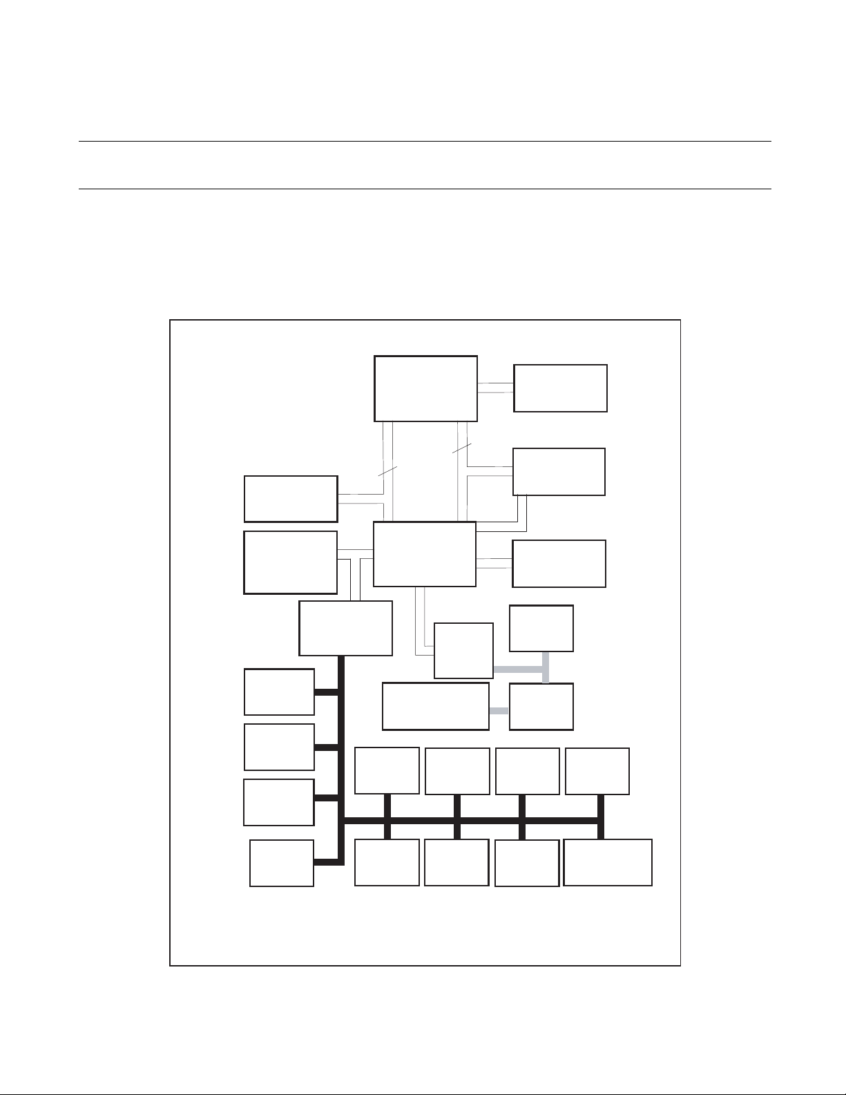
Figure 1.2-1 is a block diagram of the MB91319.
■ Block Diagram
Figure 1.2-1 Block Diagram
CHAPTER 1 OVERVIEW
Bit search
RAM
EVA 64KB
FLASH 48KB
MASK 32KB
Clock
control
Interrupt
controller
External
interrupt
32
32 to 16
adapter
FR
CPU Core
Bus converter
Font ROM
FLASH 512 KB*
ROM 384 KB*
UART
5ch
32
External
memory
I/F
2
C
I
4ch
2
2
A/D
10ch
DSU*
Flash 1MB
MASK 512KB
DMAC5ch
USB
function
OSDC
CCD
2ch
1
Port
PWC
4ch
PPG
4ch
Reload
timer 3ch
Multifunction
timer 4ch
*1 : DSU is loaded only in MB91FV319A/R
*2 : Font ROM: MB91FV319A/R: FLASH 512 KB
: MB91F318A/S, MB91316 : MASK ROM 384 KB
7
Page 30
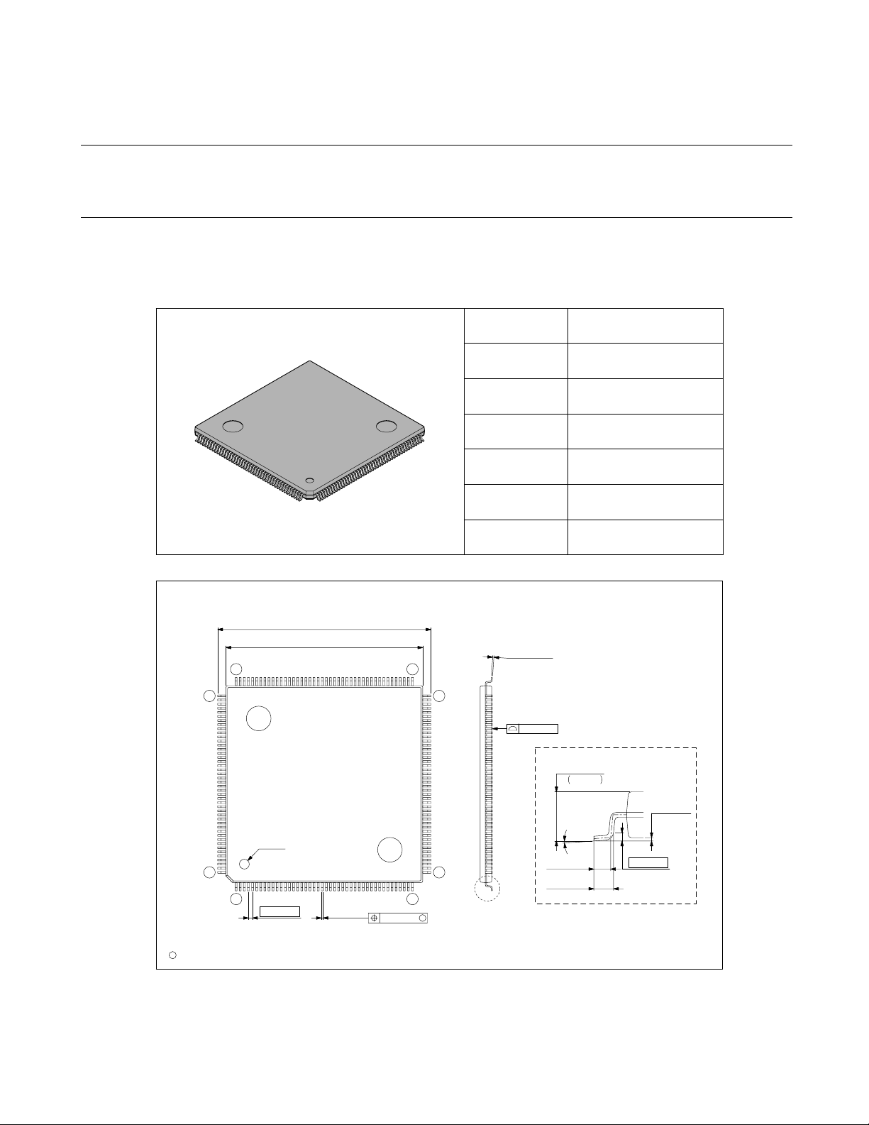
CHAPTER 1 OVERVIEW
176-pin plastic LQFP Lead pitch 0.50 mm
Package width ×
package length
24.0 × 24.0 mm
Lead shape Gullwing
Sealing method Plastic mold
Mounting height
1.70 mm MAX
Code
(Reference)
P-LQFP-0176-2424-0.50
176-pin plastic LQFP
(FPT-176P-M07)
(FPT-176P-M07)
C
2004 FUJITSU LIMITED F176013S-c-1-1
Details of "A" part
0˚~8˚
0.50±0.20
(.020±.008)
0.60±0.15
(.024±.006)
0.25(.010)
(Stand off)
(.004±.004)
0.10±0.10
1.50
+0.20
–0.10
+.008
–.004.059
(Mounting height)
0.08(.003)
(.006±.002)
0.145±0.055
"A"
INDEX
1
LEAD No.
44
45
88
89132
133
176
0.50(.020)
0.22±0.05
(.009±.002)
M
0.08(.003)
*24.00±0.10(.945±.004)SQ
26.00±0.20(1.024±.008)SQ
Dimensions in mm (inches).
Note: The values in parentheses are reference values.
Note 1)* : Values do not include resin protrusion.
Resin protrusion is +0.25(.010)Max(each side).
Note 2) Pins width and pins thickness include plating thickness
Note 3) Pins width do not include tie bar cutting remainder.
1.3 External Dimensions
The MB91319 is available in one type of package.
Figure 1.3-1 shows the dimensions of the MB91319.
■ Dimensions of the MB91319
Figure 1.3-1 External Dimensions of MB91319
8
Page 31

1.4 Pin Layout
This section shows the pin layout of the MB91319.
■ Pin Layout of the MB91 319
Figure 1.4-1 is a diagram of the pin layout of the MB91319 .
Figure 1.4-1 Pin Layout of the MB91319
VSYNC
DOCKI
DCKOFHVOB1
VOB2
176
175
174
VDDIR2R1R0G2G1G0B2B1B0UDP
173
172
171
170
169
168
167
166
165
164
163
162
161
160
UDM
159
VDDE
X0B
158
157
VSS
156
X1B
155
VDDI
154
PB7
153
PB6
152
PB5
151
PB4
150
PB3
149
PB2
148
PB1
147
PB0
146
P17
145
P16/ATRG
P15/PPG3
144
143
P14/PPG2
P13/PPG1
P12/PPG0
142
141
140
CHAPTER 1 OVERVIEW
P11/TMO3
P10/TMO2
P07/TMO1
P06/TMO0
P05/TOUT2
P04/TOUT1
P03/TOUT0
139
138
137
136
135
134
133
HSYNC1
HSYNC2
HSYNC3
VDDDE
VSS
VGS1/BCI1
CP01
VSSP1
VDDP1
VGS2/BCI2
CP02
VSSP2
VDDP2
VGS3/BCI3
CP03
VSSP3
VDDP3
VDDR
VRef(1.1V)
VR0(2.7kΩ)
ROUT
VSSR
VDDG
GOUT
VSSG
VDDB
BOUT
VSSB
VIN0
VIN1
VDDIS
VSSS
VDDI
AVCC
AVRH
AVSS/AVRL
PC0/AN0
PC1/AN1
PC2/AN2
PC3/AN3
PC4/AN4
PC5/AN5
PC6/AN6
PC7/AN7
1
2
3
4
5
6
7
8
9
10
11
12
13
14
15
16
17
18
19
20
21
22
23
24
25
26
27
28
29
30
31
32
33
34
35
36
37
38
39
40
41
42
43
44
4546474849505152535455565758596061626364656667686970717273747576777879
X1
VSS
X0
VDDE
P32
P31
P30
P27
P26
P25
P24
P23
P22
P21/AN9
P20/AN8
TOP VIEW
LQFP-176
MB91FV319A/R
MB91F318A/S
MB91316
ICS1
ICS0
IBREAK
ICLK
TRSTX
VDDI
ICS2
ICD0
ICD1
ICD2
ICD3
MD0
MD1
MD2
MD3
P80/SCL0
INITX
P82/SCL1
P81/SDA0
80
81828384858687
P86/SCK0
P85/SO0
P84/SI0
P83/SDA1
P90/SO1
P87/SI1
P93/TMI0
P92/RIN
P91/SCK1
132
131
130
129
128
127
126
125
124
123
122
121
120
119
118
117
116
115
114
113
112
111
110
109
108
107
106
105
104
103
102
101
100
88
P94/TMI1
P02/SCK4/TIN2
P01/SO4/TIN1
P00/SI4/TIN0
P74
P73
P72
P71
P70
VDDE
VSS
VDDI
P57
P56
P55
P54
P53
P52/SCK3
P51/SO3
P50/SI3
P47/SCK2
P46/SO2
P45/SI2
P44/SDA4
P43/SDA3
P42/SCL4
P41/SCL3
P40/SDA2
P37/SCL2
P36/TRG3
P35/TRG2
P34/TRG1
P33/TRG0
NMIX
99
PA2/INT3
98
PA1/INT2
97
PA0/INT1
96
VDDI
95
X1A
94
VSS
93
X0A
92
VDDE
91
P97/INT0
90
P96/TMI3
89
P95/TMI2
Note: Do not be connected anything to TRST, ICS2 to ICS0, ICD3 to ICD0, ICLK and IBREAK pins on MB91FV319AR.
Because these pins are used as open pins on MB91F318A/S, and MB91316.
9
Page 32

CHAPTER 1 OVERVIEW
1.5 List of Pin Functions
This section describes the pin functions of the MB91319.
■ List of Pin Functions
Table 1.5-1 lists the pin functions.
Table 1.5-1 Pin Functions of the MB91319 (1 / 7)
Pin number Pin name I/O circuit type Function
1 HSYNC1 G Horizontal synchronous input 1
2 HSYNC2 G Horizontal synchronous input 2
3 HSYNC3 G Horizontal synchronous input 3
4 VDDE - I/O power supply
5 VSS - Ground
6 VGS1/VCI1 - Guard band ground
7 CPO1 K Charge pump output
8 VSSP1 - Dot clock PLL ground
9 VDDP1 - Dot clock PLL power supply (2.5 V)
10 VGS2/VCI2 - Guard band ground
11 CPO2 K Charge pump output
12 VSSP2 - Dot clock PLL ground
13 VDDP2 - Dot clock PLL power supply (2.5 V)
14 VGS3/VCI3 - Guard band ground
15 CPO3 K Charge pump output
16 VSSP3 - Dot clock PLL ground
17 VDDP3 - Dot clock PLL power supply (2.5 V)
18 VDDR - D/A power supply for Red
19 VREF(1.1V) K Voltage reference input
20 VRO(2.7kΩ) K Resistor connection pin
21 ROUT K Output for Red (analog)
22 VSSR - D/A ground for Red
23 VDDG - D/A power supply for Green
24 GOUT K Output for Green (analog)
25 VSSG - D/A ground for Green
26 VDDB - D/A power supply for Blue
27 BOUT K Output for Blue (analog)
28 VSSB - D/A ground for Blue
29 VIN0 K Data slicer input 0
30 VIN1 K Data slicer input 1
10
Page 33

Table 1.5-1 Pin Functions of the MB91319 (2 / 7)
Pin number Pin name I/O circuit type Function
31 VDDIS - Data slicer power supply (2.5 V)
32 VSSS - Data slicer ground
33 VDDI - Internal logic power supply (2.5 V)
34 AVCC - A/D power supply
35 AVRH - A/D reference power supply
36 AVSS/AVRL - A/D ground
37
38
39
40
41
42
43
44
45
46
47 P22 C Gene r al- pu rp o se po r t
48 P23 C Gene r al- pu rp o se po r t
49 P24 C Gene r al- pu rp o se po r t
50 P25 C Gene r al- pu rp o se po r t
51 P26 C Gene r al- pu rp o se po r t
52 P27 C Gene r al- pu rp o se po r t
53 P30 C Gene r al- pu rp o se po r t
54 P31 C Gene r al- pu rp o se po r t
55 P32 C Gene r al- pu rp o se po r t
56 VDDE - 3.3 V power supply
57 X0 A 10 MHz oscillation pin
58 VSS - Ground
59 X1 A 10 MHz oscillation pin
PC0
AN0 Analog input
PC1
AN1 Analog input
PC2
AN2 Analog input
PC3
AN3 Analog input
PC4
AN4 Analog input
PC5
AN5 Analog input
PC6
AN6 Analog input
PC7
AN7 Analog input
P20
AN8 Analog input
P21
AN9 Analog input
E
E
E
E
E
E
E
E
E
E
General-purpose port
General-purpose port
General-purpose port
General-purpose port
General-purpose port
General-purpose port
General-purpose port
General-purpose port
General-purpose port
General-purpose port
CHAPTER 1 OVERVIEW
11
Page 34

CHAPTER 1 OVERVIEW
Table 1.5-1 Pin Functions of the MB91319 (3 / 7)
Pin number Pin name I/O circuit type Function
60 VDDI - Internal logic power supply (2.5 V)
61
62
63
64
65
66
67
68
69
70
TRSTX
ICLK
IBREAK
ICS0
ICS1
ICS2
ICD0
ICD1
ICD2
ICD3
B
M
L
O
O
O
P
P
P
P
DSU tool reset (this pin is open in the MB91F31x model
series. DO NOT CONNECT)
DSU clock (this pin is open in the MB91F31x model series.
DO NOT CONNECT)
DSU break (this pin is open in the MB91F31x model series.
DO NOT CONNECT)
DSU status (this pin is open in the MB91F31x model series.
DO NOT CONNECT)
DSU status (this pin is open in the MB91F31x model series.
DO NOT CONNECT)
DSU status (this pin is open in the MB91F31x model series.
DO NOT CONNECT)
DSU data (this pin is open in the MB91F31x model series.
DO NOT CONNECT)
DSU data (this pin is open in the MB91F31x model series.
DO NOT CONNECT)
DSU data (this pin is open in the MB91F31x model series.
DO NOT CONNECT)
DSU data (this pin is open in the MB91F31x model series.
DO NOT CONNECT)
71 M D0 F Mode pin
72 M D1 F Mode pin
73 M D2 F Mode pin
74 M D3 L Mode pin
75 INITX B Initial (res et) pin
76
77
78
79
80
81
82
83
P80
SCL0 I
J
P81
SDA0 I
J
P82
SCL1 I
J
P83
SDA1 I
J
P84
SI0 UART 0 serial input
C
P85
SO0 UART 0 serial output
C
P86
SCK0 UART 0 clock I/O
C
P87
SI1 UART 1 serial input
C
General-purpose port
2
C clock pin
General-purpose port
2
C data pin
General-purpose port
2
C clock pin
General-purpose port
2
C data pin
General-purpose port
General-purpose port
General-purpose port
General-purpose port
12
Page 35

Table 1.5-1 Pin Functions of the MB91319 (4 / 7)
Pin number Pin name I/O circuit type Function
84
85
86
87
88
89
90
91
P90
SO1 UART 1 serial output
C
P91
SCK1 UART 1 clock I/O
C
P92
RIN PWC input
C
P93
TMI0 Multifunction timer 0 input
C
P94
TMI1 Multifunction timer 1 input
C
P95
TMI2 Multifunction timer 2 input
C
P96
TMI3 Multifunction timer 3 input
C
P97
INT0 External interrupt input 0
O
General-purpose port
General-purpose port
General-purpose port
General-purpose port
General-purpose port
General-purpose port
General-purpose port
General-purpose port
92 VDDE - 3.3 V power supply
93 X0A A 32 kHz oscillation pin
94 VSS - Ground
95 X1A A 32 kHz oscillation pin
96 VDDI - Internal logic power supply (2.5 V)
97
98
99
PA0
INT1 External interrupt input 1
O
PA1
INT2 External interrupt input 2
O
PA2
INT3 External interrupt input 3
O
General-purpose port
General-purpose port
General-purpose port
100 NMIX B NMIX input
101
102
103
104
105
P33
TRG0 PPG 0 trigger input
C
P34
TRG1 PPG 1 trigger input
C
P35
TRG2 PPG 2 trigger input
C
P36
TRG3 PPG 3 trigger input
C
P37
SCL2 I
N
General-purpose port
General-purpose port
General-purpose port
General-purpose port
General-purpose port
2
C clock pin
CHAPTER 1 OVERVIEW
13
Page 36

CHAPTER 1 OVERVIEW
Table 1.5-1 Pin Functions of the MB91319 (5 / 7)
Pin number Pin name I/O circuit type Function
107
108
106
109
110
111
112
113
114
115
116
117
118
119
120
121
P41
N
SCL3 I
P42
SCL4 I
P40
SDA2 I
P43
N
N
N
SDA3 I
P44
SDA4 I
N
P45
SI2 UART 2 serial input
C
P46
SO2 UART 2 serial output
C
P47
SCK2 UART 2 clock I/O
C
P50
SI3 UART 3 serial input
C
P51
SO3 UART 3 serial output
C
P52
SCK3 UART 3 clock I/O
C
P53
CS7X Chip select
C
P54
CS6X Chip select
C
P55
CS5X Chip select
C
P56
CS4X Chip select
C
P57
CS0X Chip select
C
General-purpose port
2
C clock pin
General-purpose port
2
C clock pin
General-purpose port
2
C data pin
General-purpose port
2
C data pin
General-purpose port
2
C data pin
General-purpose port
General-purpose port
General-purpose port
General-purpose port
General-purpose port
General-purpose port
General-purpose port
General-purpose port
General-purpose port
General-purpose port
General-purpose port
122 VDDI - Internal logic power supply (2.5 V)
123 VSS - Ground
124 VDDE - 3.3 V power supply
125 P70 C General-purpose port
126 P71 C General-purpose port
127 P72 C General-purpose port
128 P73 C General-purpose port
14
Page 37

Table 1.5-1 Pin Functions of the MB91319 (6 / 7)
Pin number Pin name I/O circuit type Function
129 P74 C General-purpose port
P00
130
131
132
133
134
135
136
137
138
139
140
141
142
143
144
145 P17 C General-purpose port
146 PB0 C General-purpose port
147 PB1 C General-purpose port
148 PB2 I General-purpose port
149 PB3 C General-purpose port
SI4 UART 4 serial input
TIN0 Reload timer 0 trigger input
P01
SO4 UART 4 serial output
TIN1 Reload timer 1 trigger input
P02
SCK4 UART 4 clock I/O
TIN2 Reload timer 2 trigger input
P03
TOUT0 Reload timer 0 output
P04
TOUT1 Reload timer 1 output
P05
TOUT2 Reload timer 2 output
P06
TMO0 Multifunction timer 0 output
P07
TMO1 Multifunction timer 1 output
P10
TMO2 Multifunction timer 2 output
P11
TMO3 Multifunction timer 3 output
P12
PPG0 PPG 0 output
P13
PPG1 PPG 1 output
P14
PPG2 PPG 2 output
P15
PPG3 PPG 3 output
P16
ATRG A/D conversion trigger input
C
C
C
C
C
C
C
C
C
C
C
C
C
C
C
General-purpose port
General-purpose port
General-purpose port
General-purpose port
General-purpose port
General-purpose port
General-purpose port
General-purpose port
General-purpose port
General-purpose port
General-purpose port
General-purpose port
General-purpose port
General-purpose port
General-purpose port
CHAPTER 1 OVERVIEW
15
Page 38

CHAPTER 1 OVERVIEW
Table 1.5-1 Pin Functions of the MB91319 (7 / 7)
Pin number Pin name I/O circuit type Function
150 PB4 C General-purpose port
151 PB5 C General-purpose port
152 PB6 H General-purpose port
153 PB7 C General-purpose port
154 VDDI - Internal power supply (2.5 V)
155 X1B A 48 MHz oscillation pin
156 VSS - Ground
157 X0B A 48 MHz oscillation pin
158 VDDE - 3.3 V power supply
159 UDM
160 UDP USP-Function
161 B0 D RGB digital output
162 B1 D RGB digital output
163 B2 D RGB digital output
164 G0 D RGB digital output
165 G1 D RGB digital output
166 G2 D RGB digital output
167 R0 D RGB digital output
168 R1 D RGB digital output
169 R2 D RGB digital output
170 VDDI - Internal logic power supply (2.5 V)
171 VOB2 D Semi-transparent color period output
172 VOB1 D OSD display period output
173 FH D Horizontal synchronous output
174 DCKO D Dot clock output
175 DOCKI G Dot clock input
176 VSYNC G Vertical synchronous output
USB
USB-Function
16
Page 39

CHAPTER 1 OVERVIEW
1.6 Input-output Circuit Forms
This section describes the input-output circuit types of the MB91319.
■ Input-Output Circuit Types
Table 1.6-1 lists the input-output circuit types of the MB91319.
Table 1.6-1 Input-Output Circuit Types of the MB91319 (1 / 6)
Classification Circuit type Remarks
Oscillation feedback
X1
A
XO
Standby control
Clock input
CMOS level hysteresis input with pull-up
resistors
B
Digital input
• CMOS level output
CMOS level hysteresis input with
standby control
Digital output
C
Standby control
Digital output
Digital input
17
Page 40

CHAPTER 1 OVERVIEW
Table 1.6-1 Input-Output Circuit Types of the MB91319 (2 / 6)
Classification Circuit type Remarks
2.5 V CMOS level output
2.5V
Digital output
CMOS level hysteresis input with
standby control
D
Standby control
Digital output
Digital input
CMOS level output
CMOS level hysteresis input with
standby control
Digital output
Digital output
Use of analog input switch
E
Analog input
Control
Digital input
18
Standby control
CMOS level input without standby control
F
Digital input
Page 41

CHAPTER 1 OVERVIEW
Table 1.6-1 Input-Output Circuit Types of the MB91319 (3 / 6)
Classification Circuit type Remarks
CMOS level hysteresis input without
standby control
G
Digital input
CMOS level output
CMOS level hysteresis input with
Pull down control
Digital output
standby control and pull-down resistor
H
Standby control
Digital output
Digital input
CMOS level output
CMOS level hysteresis input with
standby control and pull-up resistor
Digital output
I
Standby control
Digital output
Digital input
19
Page 42

CHAPTER 1 OVERVIEW
Table 1.6-1 Input-Output Circuit Types of the MB91319 (4 / 6)
Classification Circuit type Remarks
Open-drain output
CMOS level hysteresis input with
standby control provided
Open-drain
control
J
Standby control
Digital output
Digital input
Analog pin
K
CMOS level hysteresis input with pulldown resistor
20
L
Digital input
Page 43

CHAPTER 1 OVERVIEW
Table 1.6-1 Input-Output Circuit Types of the MB91319 (5 / 6)
Classification Circuit type Remarks
CMOS level output
Digital output
M
Digital output
2
3 ports for I
C
CMOS level hysteresis input
CMOS level output
Open-drain
control
Use of stop control
Digital output
Digital input
Control
Digital input
Control
N
Open-drain
control
Digital output
Digital input
Open-drain
control
Digital output
21
Page 44

CHAPTER 1 OVERVIEW
Table 1.6-1 Input-Output Circuit Types of the MB91319 (6 / 6)
Classification Circuit type Remarks
CMOS level output
CMOS level hysteresis input without
standby control
Digital output
O
Digital output
Digital input
CMOS level output
CMOS level hysteresis input without
standby control
Digital output
Use of pull-down resistor
P
Digital output
Digital input
22
Page 45

CHAPTER 2
HANDLING THE DEVICE
This chapter provides precautions on handling the
MB91319 series.
2.1 Precautions on Handling the Device
23
Page 46

CHAPTER 2 HANDLING THE DEVICE
2.1 Precautions on Handling the Device
This section contains information on preventing a latch up and on the handling of pins.
■ Preventing a Latch Up
A latch up can occur if, on a CMOS IC, a voltage higher than VCC or a voltage lower than VSS is
applied to an input or output pin or a voltage higher than the rating is applied between VCC and
VSS. A latch up, if it occurs, significantly increases the power supply current and may cause
thermal destruction of an element. When you use a CMOS IC, be very careful not to exceed the
maximum rating.
■ Unused Input Pins
Do not leave an unused input pin open, since it may cause a malfunction. Handle by, for
example, using a pull-up or pull-down resistor.
■ Power Supply Pins
If more than one VCC or VSS pin exists, those that must be kept at the same potential are
designed to be connected to one other inside the device to prevent malfunctions such as latch up.
Be sure to connect the pins to a power supply and ground external to the device to minimize
undesired electromagnetic radiation, prevent strobe signal malfunctions due to an increase in
ground level, and conform to the total output current rating. Given consideration to connecting the
current supply source to VCC and VSS of the device at the lowest impedance possible.
It is also recommended that a ceramic capacitor of around 0.1 µF be connected between VCC
and VSS at circuit points close to the device as a bypass capacitor.
■ Quartz Oscillation Circuit
Noise near the X0 or X1 pin may cause the device to malfunction. Design printed circuit boards
so that X0, X1, the quartz oscillator (or ceramic oscillator), and the bypass capacitor to ground
are located as near to one another as possible.
It is strongly recommended that printed circuit board artwork that surrounds the X0 and X1 pins
with ground be used to increase the expectation of stable operation.
Please ask the crystal maker to evaluate the oscillation characteristics of the crystal and this
device.
■ Mode Pins (MD0 to MD3)
These pins must be directly connected to VCC or VSS when they are used. Keep the pattern
length between a mode pin on a printed circuit board and VCC or VSS as short as possible so
that they can be connected at a low impedance.
■ Tool Reset Pins (TRST
Be sure to input the same signal as the INIT
processing is executed for the product.
24
)
, when this pin is not used for the tool. The same
Page 47

■ Power-on
CHAPTER 2 HANDLING THE DEVICE
Immediately after power-on, be sure to apply a reset with the INIT pin to initialize the settings
(INIT).
Also immediately after power-on, keep the INIT
the required frequency stability. (For initialization by INIT from the INIT
stabilization wait time is set to the minimum value.)
■ Source Oscillation Input at Power-on
At power-on, be sure to input a source clock until the oscillation stabilization wait time is reached.
■ Precautions at Power-On/Power-Off
❍ Precautions when turning on and off VDDI (intern al 2.5 V po wer suppl y) and VDDE (e xternal
3.3 V power supply)
To ensure the reliability of LSI devices, do not continuously apply only VDDE (external) when
VDDI (internal) is off.
When VDDE (external) is changed from off to on, the power noise may make it impossible to
retain the internal state of the circuit.
• Power-on: VDDI (internal) → analog → VDDE (external) → signal
• Power-off: Signal → VDDE (external)→ analog → VDDI (internal)
■ Clocks
pin at the L level until the oscillator has reached
pin, the oscillation
❍ Notes on using external clock
When using an external clock under normal conditions, supply clock signals to X0 (X0A, X0B)
pins and simultaneously supply the antiphase signals to X1 (X1A, X1B) pins. In this case,
however, do not use STOP mode (oscillation stop mode) because in the STOP mode, the X1
(X1A, X1B) pins stop at "H" output state. When operating at 12.5 MHz or lower frequency,
however, the clock signal input is needed only to the X0 (X0A, X0B) pins.
Examples of using an external clock are illustrated in Figure 2.1-1 and Figure 2.1-2.
Figure 2.1-1 Circuit Using External Clock (Normal)
X0, X0A, X0B
X1, X1A, X1B
MB91FV319A/MB91F318A
[STOP mode (oscillation stop mode) cannot be used.]
Figure 2.1-2 Circuit Using External Clock (12.5 MHz or Lower)
X0, X1A, X1B
OPEN
X1, X1A, X1B
MB91FV319A/MB91F318A
25
Page 48

CHAPTER 2 HANDLING THE DEVICE
Note:
Signal delay time between the X0 (X0A, X0B) and X1 (X1A, X1B) pins must be within
15 ns (operating at 10 MHz).
❍ Notes on using MS clock
For MSCLK, MS transfer clock signal is output externally from an internal I/O cell and then
reentered. Therefore, insert damping resistor exteriorly to reduce reflection noise that may affect
the internal circuit.
■ Limitations
❍ Common of MB91319 series
Clock controller
INIT
must be kept at the L level until the oscillation stabilization wait time is reached.
Bit search module
Data register for detection 0 (BSD0), data register for det ection 1 (BSD1) , and d ata regis ter for
change point detection BSDC are word access only.
I/O port
Only byte access is permitted for ports.
Low Power Consumption Mode
To switch to standby mode, use synchronous standby mode (set by the SYNCS bit, that is bit8
of the TBCR, time-base counter control register) and be sure to use the following sequence:
/* STCR write */
ldi #_STCR, r0 ; STCR register (0x0481)
ldi #val_of_Stby, rl ; Val_of_Stby is write data to STCR
stb rl, @r0 ; Write to STCR
/* CTBR write */
ldi #_CTBR, r2 ; CTBR register (0x0483)
ldi #0xA5, rl ; Clear command (1)
stb rl, @r2 ; Write A5 to CTBR
ldi #0x5A, rl ; Clear command (2)
stb rl, @r2 ; Write 5A to CTBR
/* Time base counter is cleared here */
ldub @r0, rl ; Read STCR
/* Synchronous standby transition start */
ldub @r0, rl ; Dummy read STCR
nop ; nop ×5 for timing adjustment
nop
nop
nop
nop
When using the monitor debugger, do not:
• Set a break point within the above sequence of instructions.
• Step of the instructions within the above sequence of instructions.
26
Page 49

CHAPTER 2 HANDLING THE DEVICE
Prefetch
When allowing prefetch in the little endian area, only word access (in 32-bit word) should be
used to access the area.
Byte access and half-word access are not workin g pr op e rly.
Notes on using PS register
PS register is processed by some instructions in advance so that exception operations as
stated below may cause breaks during interruption handling routine when using debugger,
and may cause updates to the display contents of PS flags.
In either case, this device is designed to carry out reprocessing properly after returning from
such EIT events. The operations before and after the events are performed as prescribed in
the specification.
1. The following operations may be performed (c) if an instruction immediately before a data
event or a DIVOU/DIVOS emulator menu instruction (a) receives a user interrupt/NMI, or (b)
breaks during stepping.
• D0 and D1 flags are updated in advance.
• EIT handling routine (u ser interrupt/NMI, or emulator) is executed.
• After returning from the EIT, a DIVOU/DIVOS instruction is e xecuted and the D0 and D1
flags are updated to the same values as in (1).
2. The following operations are performed if each instruction from ORCCR, STILM, MOV Ri and
PS is executed to allow an interruption while user interrupt/NMI trigger exists.
• PS register is updated in advance.
• EIT handling routine (user interrupt/NMI) is executed.
• After returning from the EIT, the above instructions are executed and the PS register is
updated to the same value as in (1).
Watchdog Timer Function
The watchdog timer equipped in this model operates to monitor programs to ensure that they
execute reset defer function within a certain period of time, and to reset the CPU if the reset
defer function is not executed due to the program runaway. For that reason, once the
watchdog timer function is enabled, it keeps its operation until it is reset.
By way of exception, the watchdog timer automatically defers a reset under the condition
where the CPU program executions are stopped. For more detail, refer to the description
section of the watchdog timer function.
If the system gets out of control and the situation becomes as mentioned above, watchdog
reset may not be generated. In that case, please rese t (IN IT) fro m the exte rn al INI T
pin.
Note on using A/D
Nevertheless the MB91319 series contains an A/D converter, be sure not to apply the higher
power supply than V
to the AVCC.
CC
About Software Reset of Synchronous Mode
To use the software reset of synchronous mode, be sure to meet the following 2 conditions.
• Set interrupt enable flag (I-Flag) to "disabled" (I-Flag= 0)
• Do not use NMl
27
Page 50

CHAPTER 2 HANDLING THE DEVICE
❍ Unique characteristic of the evaluation chip MB91FV319A/R
Simultaneous occurrences of software break and user interrupt/NMI (MB91FV319A/R only)
If software break and user interrupt/NMI occur together, emulator debugger may:
• Stop at a point other than the programmed break points.
• Not reexecute properly after halting.
If such failures occur, use hardware break instead of software break. When using monitor
debugger, do not set any break points within the corresponding instructions.
Stepping of the RETI Instruction
In the environment where interruptions occur frequently during stepping, the RETI is executed
repeatedly for the corresponding interrupt process routines after the stepping. As the result of
it, the main routine and low-interrupt-level programs are not executed. To avoid this situation,
do not step the RETI instruction. Otherwise, perform debugging by disabling the interruptions
when the debug on the corresponding interrupt ro utines becomes unnecessary.
Operand Break
Do not set the access to the areas containing the address of stack pointer as a target of data
event break.
Sample Batch File for Configuration
When a program is downloaded to internal RAM to execute debug, be sure to execute the
following batch file after RESET.
#------------------------------------------------------------------------------# Set MODR (0x7fd) = Enable In memory + 16bit External Bus
set mem/byte 0x7fd=0x5
#-------------------------------------------------------------------------------
28
Page 51

CHAPTER 3
CPU AND CONTROL UNITS
This chapter provides basic information required to
understand the functions of the MB91319 series. It
covers architecture, specifications, and instructions.
3.1 Memory Space
3.2 Internal Architecture
3.3 Programming Model
3.4 Data Configuration
3.5 Word Alignment
3.6 Memory Map
3.7 Branch Instructions
3.8 EIT (Exception, Interrupt, and Trap)
3.9 Operating Modes
3.10 Reset (Device Initialization)
3.11 Clock Generation Control
3.12 Device State Control
3.13 Watch Timer
3.14 Main Clock Oscillation Stabilization Wait Timer
29
Page 52

CHAPTER 3 CPU AND CONTROL UNITS
3.1 Memory Space
The MB91319 has a logical address space of 4 GB (232 addresses), which the CPU
accesses linearly.
■ Memory Space
32
The MB91319 has a logical address space of 4GB (2
lineally.
❍ Direct addressing area
The areas in the address space listed below are used for input-output.
These areas called the direct addressing area. The address of an operand can be directly
specified in an instruction.
The size of the direct addressing area varies according to the size of data to be accessed:
• Byte data access : 000
• Half word data access: 000H to 1FF
• Word data access : 000H to 3FF
to 0FF
H
H
H
H
addresses), while the CPU access
■ Memory Map
Figure 3.1-1 shows the memory space of this product.
Figure 3.1-1 Memory Map
Single-chip mode
I/O
I/O
Access disabled
Font RAM
Internal RAM *
Access disabled
Access disabled
USB-FUNC
OSDC
FlashROM1
FlashROM2
1MB *
512KB *
2
3
Access disabled
0000 0000
Direct addressing area
0000 0400
Refer to I/O map
0001 0000
0002 F800
0003 0000
1
0004 0000
0005 0000
0006 0000
0007 0000
0008 0000
Program
0018 0000
Font
0020 0000
FFFF FFFF
H
H
H
H
H
H
H
H
H
H
H
H
H
30
*1: Internal RAM area of MB91F318A/S and MB91FV319R becomes 0003 4000H to 0003 FFFFH.
Internal RAM area of MB91316 becomes 0003 8000H to 0003 FFFFH.
*2: For the MB91316, MASK ROM 512KB is used (0008 0000H to 000F FFFFH).
*3: For the MB91F318A/S, MB91316, MASK ROM 384KB is used (0008 0000H to 0019 7FFFH).
Page 53

CHAPTER 3 CPU AND CONTROL UNITS
3.2 Internal Architecture
The MB91319 CPU is a high-performance core that is designed based on a RISC
architecture with high-level function instructions for embedded applications.
■ Features
❍ RISC architecture used
Basic instruction: One instruction per cycle
❍ 32-bit architecture
General-purpose register: 32 bits × 16
❍ 4 GB linear memory space
❍ Multiplier installed
• 32-bit by 32-bit multiplication: 5 cycles
• 16-bit by 16-bit multiplication: 3 cycles
❍ Enhanced interrupt processing function
• Quick response speed: 6 cycles
• Support of multiple interrupts
• Level mask function: 16 levels
❍ Enhanced instructions for I/O operations
• Memory-to-memory transfer instruction
• Bit-processing instructions
❍ Efficient code
Basic instruction word length: 16 bits
❍ Low-power consumption
Sleep and stop modes
❍ Gear function
31
Page 54

CHAPTER 3 CPU AND CONTROL UNITS
■ Internal Architecture
The FR CPU uses the Harvard architecture, in which the instruction bus and data buses are
independent of each other.
A 32-bit ↔ 16-bit bus converter is connected to the 32-bit bus (F-bus) to provide an interface
between the CPU and peripheral resources. A Harvard ↔ Princeton bus converter is connected
to the I-bus and D-bus to provide an interface be tw ee n th e CPU an d th e bu s c ontroller.
Figure 3.2-1 shows connections in the internal architecture.
Figure 3.2-1 Internal Architecture
D-bus
FRex CPU
I-bus
Data
RAM
32 bits
16 bits
Bus converter
D address
D data
Address
Data
I address
I data
32
32
32
32
32
32
Harvard
Princeton
bus
converter
External address
24
External data
16
32
16
R-bus
Peripheral resources
F-bus
Bus controllersInternal I/O
Page 55

CHAPTER 3 CPU AND CONTROL UNITS
❍ CPU
The CPU is a compact implementation of the 32-bit RISC FR architecture.
Five instruction pipe lines are used to execute one instruction per cycle. A pipeline consists of the
following stages:
• Instruction fetch (IF): Outputs an instruction address to fetch an instructio n.
• Instruction decode (ID): Decodes a fetched instruction. Also reads a register.
• Execution (EX): Execute s an arithmetic operation.
• Memory access (MA): Performs a load or store access to memory.
• Write-back (WB): Writes an operation result (or loaded memory data) to a register.
Figure 3.2-2 Instruction Pipelines
CLK
Instruction 1
Instruction 2
Instruction 3
Instruction 4
Instruction 5
Instruction 6
Instructions are never executed randomly. If Instruction A enters a pipeline before Instruction B, it
always reaches the write-back stage before Instruction B.
In general, one instruction is executed per cycle. However, multiple cycles are required to
execute a load/store instructio n with a m emory wait, a branch instr uctio n with out a delay slot, or a
multiple-cycle instruction. The execution of instructions slows down if the instructions are not
supplied fast enough.
❍ 32-bit/16-bit bus converter
The 32-bit/16-bit bus converter provides an interface between the F-bus accessed with 32-bit
width and the R-bus accessed with 16-bit width and enables data access from the CPU to built-in
peripheral circuits.
WB
MA WB
EX MA WB
ID EX MA WB
IF ID EX MA WB
WBIF ID EX MA
If the CPU performs a 32-bit width access to the R bus, this bus convert er converts the access
into two 16-bit width accesses. Some of the built-in peripheral circuits have limitations on the
access bus width.
❍ Harvard/Princeton bus converter
The Harvard/Princeton bus converter coordinates instruction and data accesses of the CPU to
provide a smooth interface between it and external buses.
The CPU has a Harvard architecture with separate buses for instructions and data. On the other
hand, the bus controller that performs control of external buses has a Princeton architecture with
a single bus. The Harvard/Princeton bus converter assigns priorities to instruction and data
accesses from the CPU to control accesses to the bus controller. This function allows the order of
external bus accesses to be permanently optimized.
33
Page 56

CHAPTER 3 CPU AND CONTROL UNITS
■ Overview of Instructions
The FR supports the general RISC instruction set as well as logical operation, bit manipulation,
and direct addressing instructions optimized for embedded applications. For the instruction set,
see "APPENDIX I Instruction Lists". Each instruction is 16-bit long (except for some instructions
are 32- or 48-bit long), resulting in superior efficiency of memory use.
An instruction set is classified into the following function groups:
• Arithmetic operation
• Load and store
•Branch
• Logical operation and bit manipulation
• Direct addressing
•Other
❍ Arithmetic operation
Arithmetic operation instructions include standard arithmetic operation instructions (addition,
subtraction, and comparison) and shift instructions (logical shift and arithmetic shift). The addition
and subtraction instructions include an operation with carries for use with multiple-word-length
operations and an operation that does not change flag values, a convenience in address
calculations.
Furthermore, 32-bit-by-32-bit and 16-bit-by-16-bit multiplication instructions and a 32-bit-by-32-bit
step division instruction are provided.
Additionally, an immediate data transfer instruction that sets immediate data in a register and a
register-to-register transfer instruction are provided.
An arithmetic operation instruction is executed using the general-purpose registers and the
multiplication and division registers in the CPU.
❍ Load and store
Load and store instructions read and write to external memory. They are also used to read and
write to a peripheral circuit (I/O) on the chip.
Load and store instructions have three access lengths: byte, halfword, and word. In addition to
indirect memory addressing via general registers, indirect memory addressing via registers with
displacements and via registers with register incrementing or decrementing are provided for some
instructions.
❍ Branch
The branch group includes branch, call, interrupt, and return instructions. Some branch
instructions have delay slots while others do not. These may be optimized according to the
application. The branch instructions are described in detail later.
❍ Logical operation and bit manipulation
Logical operation instructions perform the AND, OR, and EOR logical operations between
general-purpose registers or a general-purpose register and memory (and I/O). Bit manipulation
instructions directly manipulate the contents of memory (and I/O). They access memory using
general register indirect addressing.
34
Page 57

CHAPTER 3 CPU AND CONTROL UNITS
❍ Direct addressing
Direct addressing instructions are used for access between an I/O and a general-purpose register
or between an I/O and the memory. High-speed and high-efficiency access can be achieved
since an I/O address is directly specified in an instruction instead of using register indirect
addressing. Indirect memory addressing via registers with register incrementing or decrementing
are provided for some instructions.
❍ Other types of instructions
Other types of instructions include instructions that provide flag setting, stack manipulation, sign/
zero extension, and other functions in the PS register. Also, function entry and exit instructions
that support high-level languages and register multi-load/store instructions are provided.
35
Page 58

CHAPTER 3 CPU AND CONTROL UNITS
3.3 Programming Model
This section explains the programming model in detail.
■ Basic Programming Model
Figure 3.3-1 Basic Programming Model
32 bits
[Initial value]
R0
XXXX XXXX
R1
General-purpose
register
R12
R13
R14
R15
A C
F P
S P
XXXX XXXX
0000 0000
Program counter PC
Program status PS ILM SCR CCR
H
H
H
36
Table base register TBR
Return pointer RP
System stack pointer SSP
User stack pointer USP
Multiply and divide registers MDH
MDL
Page 59

■ Registers
CHAPTER 3 CPU AND CONTROL UNITS
❍ General-purpose registers
Figure 3.3-2 General-Purpose Registers
32 bits
[Initial value]
R0 XXXX XXXX
R1
R12
R13 A C
R14 F P XXXX XXXX
R15 S P 0000 0000
H
H
H
Registers R0 to R15 are general-purpose registers. They are used as the accumulator for various
operations and pointers for memory access.
Of these 16 registers, the following registers are intended for special applications and therefore
enhanced instructions are provided for them:
R13: Virtual accumulator
R14: Frame pointer
R15: Stack pointer
The initial value after reset is not defined for R0 though R14 and is 00000000
(SSP value) for
H
R15.
❍ Program status (PS)
The program status (PS) register holds the program status and consists of three parts: ILM, SCR,
and CCR.
In the figure, all the undefined bits are reserved. During reading, 0 is always read.
This register cannot be written.
Bit location 31 20 16 10 8 7 0
ILM
SCR
CCR
37
Page 60

CHAPTER 3 CPU AND CONTROL UNITS
❍ Condition code register (CCR)
7 6 5 4 3 2 1 0
- - S I N Z V C --00XXXX
[bit5] Stack flag
Specifies the stack pointer to be used as R15.
Value Description
The system stack pointer (SSP) is used as R15.
0
When an EIT occurs, this bit is automatically set to 0.
(Note that the value saved on the stack is the value befor e it is cleared.)
1 The user stack pointer (USP) is used as R15.
Reset clears this bit to 0.
Set this bit to 0 when executing a RETI instruction.
[bit4] Interrupt enable flag
Enable or disable a user interrupt request.
Value Description
User interrupt disabled.
0
When the INT instruction is executed, this bit is cleared to 0.
(Note that the value saved on the stack is the value befor e it is cleared.)
[Initial value]
B
1
User interrupt enabled.
The mask processing of a user interrupt request is controlled by the value held in ILM.
Reset clears this bit to 0.
[bit3] Negative flag
Indicate the sign when the operation result is regarded as an integer represented by its 2's
complement.
Value Description
0 Indicates that the operation result is a positive value.
1 Indicates that the operation result is a negative value.
The initial value after reset is undefined.
[bit2] Zero flag
Indicate whether the operation result is 0.
Value Description
0 Indicates that the operation result is not 0.
1 Indicates that the operation result is 0.
38
The initial value after reset is undefined.
Page 61

CHAPTER 3 CPU AND CONTROL UNITS
[bit1] Overflow flag
Indicate whether an overflow has occurred as a result of the operation when the operand is
regarded as an integer represented by its 2's complement.
Value Description
0 Indicates that the operation did not cause an overflow.
1 Indicates that the operation caused an overflow.
The initial value after reset is undefined.
[bit0] Carry flag
Indicate whether a carry or a borrow has occurred from the most significant bit in the
operation.
Value Description
0 Indicates that no carry or borrow has occurred.
1 Indicates that a carry or borrow has occurred.
The initial value after reset is undefined.
❍ System condition code register (SCR)
10 9 8 [Initial value]
D1 D0 T XX0
B
[bit10, bit9] Step division flag
Hold the intermediate data when step division is executed.
Do not change these bits during step division.
To execute other processing during a step division, save and restore the value of the PS
register to ensure that the step division is restar te d.
The initial value after reset is undefined.
When the DIVOS instruction is executed, the multiplicand and divisor are accessed and this
flag is set.
When the DIV0U instruction is executed, this flag is cleared.
[bit8] Step trace trap flag
This bit specifies whether the step trace trap is to be enabled.
Value Description
0 The step trace trap is disabled.
The step trace trap is enabled.
1
All user NMIs and user interrupts are prohibited.
Reset clears this bit to 0.
The step trace trap function is also used by emulators. When being used by an emulator, this
function cannot be used in a user program.
39
Page 62

CHAPTER 3 CPU AND CONTROL UNITS
❍ ILM
20 19 18 17 16 [Initial value]
ILM4 ILM3 ILM2 ILM1 ILM0 01111
The interrupt level mask (ILM) register holds an interrupt level mask value. The value held in ILM
is used as a level mask.
An interrupt request to the CPU is accepted only when its interrupt level is higher than the level
indicated in this ILM.
B
The highest level is 0 (00000
), and the lowest level is 31 (11111B).
B
The program setting range is limited.
• When the original value is between 16 and 31:
A new value between 16 and 31 can be set. If an instruction that sets a value between 0 and
15 is executed, the specified value plus 16 is transferred.
• When the original value is between 0 and 15:
Any value between 0 and 31 can be set.
Reset initializes this bit to 15 (01111
).
B
❍ Program counter (PC)
31 0 [Initial value]
PC XXXXXXXX
H
[bit31 to bit0]
These are the bits of the program counter that indicates the address of the instruction being
executed.
Bit0 is set to 0 when the PC is upd ated after an instruction is executed. Bit0 can become 1
only if the branch address is an odd number address.
However, even if the branch address is an odd number address, bit0 is invalid and therefore
the instruction should be placed at an even number address.
40
The initial value after reset is undefined.
❍ Table base register (TBR)
31 0 [Initial value]
TBR 000FFC00
H
The table base register holds the first address of the vector table to be used during EIT
processing.
The initial value after reset is 000FFC00
.
H
Page 63

CHAPTER 3 CPU AND CONTROL UNITS
❍ Return pointer (RP)
31 0 [Initial value]
RP XXXXXXXXH
The return pointer holds the address returned from a subroutine.
When a CALL instruction is executed, the PC value is transferred to this RP.
When a RET instruction is executed, the RP contents are transferred to PC.
The initial value after reset is undefined.
❍ System stack pointer (SSP)
31 0 [Initial value]
SSP 00000000
SSP is the system stack pointer.
SSP functions as R15 when the S flag is 0.
SSP can also be specified explicitly.
H
This register is also used as a stack pointer that specifies the stack on which the PS and PC
contents are to be saved if an EIT occurs.
The initial value after reset is 00000000
.
H
❍ User stack pointer (USP)
31 0 [Initial value]
USP XXXXXXXX
H
USP is the user stack pointer
USP functions as R15 when the S flag is 1.
USP can also be specified explicitly.
The initial value after reset is undefined.
This register cannot be used by the RETI instruction.
41
Page 64

CHAPTER 3 CPU AND CONTROL UNITS
❍ Multiply and divide register
31 0
MDH
MDL
The multiply and divide registers are 32-bit long.
The initial value after reset is undefined.
When multiplication is executed
For a 32-bit-by-32-bit multiplication, the 64-bit long operation result is stored in the multiply
and divide registers as follows:
MDH: High-order 32 bits
MDL: Low-order 32 bits
For a 16-bit-by-16-bit multiplication, the result is stored as follows:
MDH: Undefined
MDL: 32-bit result
When division is executed
At the start of calculation, the dividend is stored in MDL.
If a DIV0S/DIV0U, DIV1, DIV2, DIV3, or DIV4S instruction is executed for a division, the result
is stored in MDL and MDH as follows:
MDH: Remainder
MDL: Quotient
42
Page 65

CHAPTER 3 CPU AND CONTROL UNITS
3.4 Data Configuration
The MB91319 uses the following two data ordering methods:
• Bit ordering
• Byte ordering
• Bit ordering
■ Bit Ordering
Use the little endian method for bit ordering.
bit 31 30 29 28 27 26 25 24 23 22 21 20 19 18 17 16 15 14 13 12 11 10 9 8 7 6 5 4 3 2 1 0
LSBMSB
■ Byte Ordering
Use the big endian method for byte ordering.
Address (n+1)
Address (n+2)
Address (n+3)
MSB LSB
Memory bit 31 23
10101010
bit
0
7
10101010Address n
11001100
11111111
00010001
15 7 0
11001100 11111111 00010001
43
Page 66

CHAPTER 3 CPU AND CONTROL UNITS
3.5 Word Alignment
Since instructions and data are accessed in byte units, the addresses at which they are
placed depend on the instruction length or the data width.
■ Program Access
A program must be placed at an address that is a multiple of 2.
Bit0 of the PC is set to 0 if the PC is updated when an instruction is executed.
Bit0 can be set to 1 only if an odd-number address is specified as the branch address.
If bit0 is set to 1, however, bit0 is invalid and an instruction must be placed at the address that is
a multiple of 2.
No odd-number address exception exists.
■ Data Access
If data is accessed, forced alignment is applied to the add re ss ba se d on the width.
Word access: An address must be a multiple of 4. (The lowest-order 2 bits are forcibly set
to 00.)
Halfword access: An address must be a multiple of 2. (The lowest-order bit is forc ibly set to
0.)
Byte access: -
During word or halfword data access, some of the bits in the result of calculating an effective
address are forcibly set to 0. For example, in @(R13, Ri) addressing mode, the register before
addition is used without change in th e calculation (even if the lowest-order bit is 1) and the loworder bits are masked. A register before calculation is not masked.
[Example] LD @(R13, R2), R0
R13 00002222
R2 00000003
H
H
+)
Addition result 00002225
H
Lower 2 bits forcibly masked
Address pin 00002224
H
44
Page 67

3.6 Memory Map
This section shows the memory map for the MB91319.
■ Memory Map
The address space is 32 bits linear.
Figure 3.6-1 Memory Map
CHAPTER 3 CPU AND CONTROL UNITS
0000 0000
0000 0100
H
H
0000 0200H
0000 0400
000F FC00
000F FFFF
FFFF FFFF
H
H
H
H
❍ Direct addressing area
Byte data
Direct addressing areaHalfword data
Word data
Vector table
initial area
The following areas in the address space are the areas for I/O. When direct addressing is used in
these areas, an operand address can be directly specified in an instruction.
The size of an address area for which an address can be directly specified varies is determined
by the data length as follows:
• Byte data (8 bits): 000
• Halfword data (16 bits): 000H to 1FF
• Word data (32 bits): 000H to 3FF
to 0FF
H
H
H
H
❍ Vector table initial area
The area from 000FFC00
to 000FFFFFH is the initial EIT vector table area.
H
You can place the vector table that will be used during EIT processing at any address by rewriting
the TBR. Initialization by a reset places the table at this address.
45
Page 68

CHAPTER 3 CPU AND CONTROL UNITS
3.7 Branch Instructions
An operation with or without a delay slot can be specified for a branch instruction used
in the MB91319.
■ Branch Instruction with Delay Slot
Instructions written as follows perform a branch operation with a de lay slot:
JMP:D @Ri CALL:D label12 CALL:D @Ri RET:D
BRA:D label9 BNO:D label9 BEQ:D label9 BNE:D label9
BC:D label9 BNC:D label9 BN:D label9 BP:D label9
BV:D label9 BNV:D label9 BLT:D label9 BGE:D label9
BLE:D label9 BGT:D label9 BLS:D label9 BHI:D label9
❍ Operation Explanation
In operation with a delay slot, the instruction located just after a branch instruction (placed in a
"delay slot") is executed before the instruction that bra nches is executed.
Since an instruction in the delay slot is executed before the branch operation, the apparent
execution speed is one cycle. However, a NOP instruction must be placed in the delay slot if
there is no valid instruction put there.
[Example]
; List of instructions
ADD R1, R2, ;
BRA:D LABEL ; Branch instruction
MOV R2, R3, ; Delay slot ... Executed before branch
...
LABEL: ST R3, @R4 ; Branch destination
If a conditional branch instruction is used, an instruction placed in the delay slot is executed
whether or not the condition for branching is met.
If a delay branch instruction is used, the order of execution for some instructions seems to be
reversed. However, this occurs only for updating the PC and the instructions are executed in the
specified order for other operations (register update and reference, etc.)
46
The following is a concrete example.
Ri referenced by the JMP:D @Ri / CALL:D @Ri instruction is not affected even though Ri is
updated by the instruction in the delay slot.
Page 69

CHAPTER 3 CPU AND CONTROL UNITS
[Example]
LDI:32 #Label, R0
JMP:D @R0 ; Branch to Label
LDI:8 #0, R0 ; No effect on the branch destination address
...
RP referenced by the RET:D instruction is not affected even though RP is updated by the
instruction in the delay slot.
[Example]
RET:D ; Branch to address defined beforehand in RP
MOV R8, RP ; No effect on the return operation
...
The flag referenced by the Bcc:D rel instruction is not affected by the instruction in the delay slot.
[Example]
ADD #1, R0 ; Flag change
BC:D Overflow ; Branch to execution result of above instruction
ANDCCR #0 ; This flag update is not referenced by the
above branch instruction.
...
If RP is referenced by an instruction in the delay slot of the CALL:D instruction, the data that has
been updated by the CALL:D instruction is read.
[Example]
CALL:D Label ; Updating RP and branching
MOV RP, R0 ; Transferring RP, execution result of above
CALL:D
...
❍ Instructions that can be placed in the delay slot
Only an instruction meeting the following conditions can be executed in the delay slot.
• One-cycle instruction
• Instruction other than a branch instruction
• Instruction whose operation is not affected even though the order is changed
A one-cycle instruction is an instruction denoted in the Number of Cycles column in the list of
instructions as 1, a, b, c, and d.
47
Page 70

CHAPTER 3 CPU AND CONTROL UNITS
❍ Step trace trap
A step trace trap does not occur between the execution of a branch instruction with a delay slot
and the delay slot.
❍ Interrupt NMI
An interrupt NMI is not accepted between the execution of a branch instruction with a delay slot
and the delay slot.
❍ Undefined instruction exception
An undefined instruction exception does not occur if there is an undefined instruction in the delay
slot. If an undefined instruction is in the delay slot, it oper ates as a NOP instruction.
■ Branch Instruction without Delay Slot
Instructions written as follows perform a branch operation without a delay slot:
JMP @Ri CALL label12 CALL @Ri RET
BRA label9 BNO label9 BEQ label9 BNE label9
BC label9 BNC label9 BN label9 BP label9
BV label9 BNV label9 BLT label9 BGE label9
BLE label9 BGT label9 BLS label9 BHI label9
❍ Operation Explanation
In operation without a delay slot, instructions are executed in the order in which they are
specified. An instruction immediately following a branch is never executed before it.
[Example]
; List of instructions
ADD R1, R2, ;
BRA LABEL ; Branch instruction (without a delay slot)
MOV R2, R3, ; Not executed
...
LABEL: ST R3, @R4 ; Branch destination
A branch instruction without a delay slot is executed in two cycles if a branch occurs and in one
cycle if no branch occurs.
Since no appropriate instruction can be placed in the delay slot, this instruction results in a more
efficient instruction code than a branch instruction with a delay slot and with NOP specified.
48
For both optimal execution speed and code efficiency, select an operation with a delay slot if a
valid instruction can be placed in the delay slot; otherwise, select an operation without a delay
slot.
Page 71

CHAPTER 3 CPU AND CONTROL UNITS
3.8 EIT (Exception, Interrupt, and Trap)
EIT, a generic term for exception, interrupt, and trap, refers to suspending program
execution if an event occurs during execution and then executing another program.
■ EIT (Exception, Interrupt, and Trap)
An exception is an event that occurs related to the execution context. Execution restarts from the
instruction that caused the exception.
An interrupt is an event that occurs independently of execution context. The event is caused by
hardware.
A trap is an event that occurs related to the execution context. Some traps, such as system calls,
are specified in a program . Execution restarts from the ins truction following the one that ca used
the trap.
■ Features
■ EIT Causes
ETI for the MB91319 has the following featur es:
• Multi-interrupt support
• Level masking function (15 levels available to the user)
• Trap instruction (INT)
• Emulator activation EIT (hardware/software)
The following are causes of EIT:
• Reset
• User interrupt (internal resource, external interrupt)
•NMI
• Delayed interrupt
• Undefined instruction exception
• Trap instruction (INT)
• Trap instruction (INTE)
• Step trace trap
• No-coprocessor trap
• Coprocessor error trap
■ Return from EIT
• RETI instruction.
49
Page 72

CHAPTER 3 CPU AND CONTROL UNITS
3.8.1 EIT Interrupt Levels
The interrupt levels are 0 to 31 and are managed with five bits.
■ Interrupt Levels
Table 3.8-1 shows the allocation of the levels.
Table 3.8-1 EIT Interrupt Levels
Level
Binary Decimal
00000
...
...
00011
00100
00101
...
...
01110
01111 15 NMI (for user)
10000
10001
...
...
11110
11111
Operation is possible for levels 16 to 31.
The interrupt level does not affect an undefined instruction exception, no-coprocessor trap,
coprocessor error trap, or an INT instruction. It does not change the ILM, either.
0
...
...
3
4
5
...
...
14
16
17
...
...
30
31
(Reserved for system)
...
...
(Reserved for system)
INTE instruction
Step trace trap
(Reserved for system)
...
...
(Reserved for system)
Interrupt
Interrupt
...
...
Interrupt
-
If the original ILM value is between
16 and 31, a program cannot set a
value in this ILM range.
User interrupts prohibited if ILM is set
Interrupts prohibited if ICR is set
■ I Flag
50
A flag that specifies whether an interrupt is permitted or prohibited. This flag is provided as bit4 of
the PS register.
Value Description
Interrupts prohibited
0
1
Cleared to 0 if the INT instruction is executed.
(Note that a value saved on the stack is the value before it is cleared.)
Interrupts permitted
The mask processing of an interrupt request is controlled by th e value in the ILM register.
Page 73

■ Interrupt Level Mask (ILM) Register
A PS register (bit20 to bit16) that holds an inte rrupt level mask value.
The CPU accepts only an interrupt request sent to it with an interrupt level higher than the level
indicated by the ILM.
CHAPTER 3 CPU AND CONTROL UNITS
The highest level is 0 (00000
Values that can be set by a program have a limit. If the original value is between 16 and 31, the
new value must be between 16 and 31. If an instruction that sets a value between 0 and 15 is
executed, the specified value plus 16 is transferred.
If the original value is between 0 and 15, any value between 0 and 31 may be set.
Note:
Use the STILM instruction to set this register.
■ Level Mask for Interrupt and NMI
If an NMI or interrupt request occurs, the interrupt level (Table 3.8-1) of the interrupt source is
compared with the level mask value held in the ILM. A request meeting the following condition is
masked and is not accepted:
Interrupt level of cause
) and the lowest level is 31 (11111B).
B
≥ Level mask value
51
Page 74

CHAPTER 3 CPU AND CONTROL UNITS
3.8.2 Interrupt Control Unit (ICR)
The interrupt control register (ICR: Interrupt Control Register), located in the interrupt
controller, sets the level of an interrupt request. An ICR is provided for each of the
interrupt request inputs. The ICR is mapped on the I/O space and is accessed from the
CPU through a bus.
■ Configuration of Interrupt Control Register (ICR)
7 6 5 4 3 2 1 0
- - - ICR4 ICR3 ICR2 ICR1 ICR0 Initial value ---11111
R R/W R/W R/W R/W
[bit4] ICR4
ICR4 is always set to 1.
B
[bit3 to bit0] ICR3 to 0
These bits are the low-order 4 bits of the interrupt level of the corresponding interrupt source.
They can be read and written to.
Together with bit4, a value between 16 and 31 can be set in the ICR.
■ Mapping of Interrupt Control Register (ICR)
Table 3.8-2 Interrupt Sources, Interrupt Control Registers, and Interrupt Vectors
Interrupt
source
Interrupt control register
IRQ00 ICR00 00000440
IRQ01 ICR01 00000441
IRQ02 ICR02 00000442
...
...
...
...
...
...
Corresponding interrupt vector
Number
Hexadecimal Decimal
H
H
H
10
11
12
H
H
H
...
...
Address
16 TBR + 3BC
17 TBR + 3B8
18 TBR + 3B4
...
...
...
...
H
H
H
52
IRQ45 ICR45 0000046D
IRQ46 ICR46 0000046E
IRQ47 ICR47 0000046F
H
H
H
3D
3E
3F
Note: See "CHAPTER 9 INTERRUPT CONTROLLER".
H
H
H
61 TBR + 308
62 TBR + 304
63 TBR + 300
H
H
H
Page 75

CHAPTER 3 CPU AND CONTROL UNITS
3.8.3 System Stack Pointer (SSP)
The system stack pointer (SSP) is used to point to the stack to save and restore data
when EIT is accepted or a return operation occurs.
■ System Stack Pointer (SSP)
bit 31 0 [Initial value]
SSP 00000000
Eight is subtracted from the register value during EIT processing and eight is added to the
register value during the return operation from EIT that occurs when the RETI instruction is
executed.
H
The system stack pointer (SSP) is initialized to 00000000
by a reset.
H
The SSP is also used as general-purpose register R15 if the S flag in the CCR is set to 0.
■ Interrupt Stack
The value in the PC or PS is saved to or restored from the area indicated by SSP. After an
interrupt occurs, the PC contents are stored at the address indicated by SSP and the PS contents
are stored at the address indicated by SSP plus 4.
Figure 3.8-1 Interrupt Stack
[Example] [Before interrupt] [After interrupt]
SSP 80000000
H
SSP 7FFFFFF8
Memory
80000000
7FFFFFFC
7FFFFFF8
H
H
H
80000000
7FFFFFFC
7FFFFFF8
H
H
H
H
PS
PC
53
Page 76

CHAPTER 3 CPU AND CONTROL UNITS
3.8.4 Table Base Register (TBR)
Indicate the beginning address of the vector table for EIT.
■ Table Base Register (TBR)
The table base register (TBR) consists of 32 bits as shown below:
bit 31 0 [Initial value]
TBR 000FFC00
Obtain a vector address by adding to the TBR the offset value predetermined for an EIT cause.
H
The table base register (TBR) is initialized to 000FFC00
■ EIT Vector Table
A 1 KB area from the address indicated in the table base register (TBR) is the vector area for EIT.
The size for each vector is 4 bytes. The relationship between a vector number and a vector
address can be expressed as follows:
The low-order two bits of the addition result are always handled as 00.
The area from 000FFC00
Special functions are allocated to some of the vectors.
Table 3.8-3 shows the vector table on the architecture.
vctadr = TBR + vctofs
= TBR + (3FC
vctadr: Vector address
vctofs: Vector offset
vct: Vector number
H
by a reset.
H
- 4 × vct)
H
to 000FFFFFH is the initial area for the vector table upon reset.
54
Page 77

Table 3.8-3 Vector Table (1 / 3)
CHAPTER 3 CPU AND CONTROL UNITS
Interrupt number
Interrupt source
Interrupt level Offset
Decimal Hexadecimal
*1
Reset
Mode vector
*1
000 -3FC
101 -3F8
Reserved for system 2 02 - 3F4
Reserved for system 3 03 - 3F0
Reserved for system 4 04 - 3EC
Reserved for system 5 05 - 3E8
Reserved for system 6 06 - 3E4
No-coprocessor trap 7 07 - 3E0
H
H
H
H
H
H
H
H
Default
address of
TBR
000FFFFC
000FFFF8
000FFFF4
000FFFF0
000FFFEC
000FFFE8
000FFFE4
000FFFE0
Coprocessor error trap 8 08 - 3DCH000FFFDC
INTE instruction 9 09 - 3D8
Instruction break exception 10 0A - 3D4
Operand break trap 11 0B - 3D0
H
H
H
000FFFD8
000FFFD4
000FFFD0
Step trace trap 12 0C - 3CCH000FFFCC
H
H
H
H
H
H
H
H
H
H
H
H
H
NMI request (tool) 13 0D - 3C8
Undefined instruction exception 14 0E - 3C4
H
H
000FFFC8
000FFFC4
NMI request 15 0F Fixed to 15(FH)3C0H000FFFC0
External Interrupt 0 16 10 ICR00 3BC
External Interrupt 1 17 11 ICR01 3B8
External Interrupt 2 18 12 ICR02 3B4
External Interrupt 3 19 13 ICR03 3B0
External Interrupt 4 20 14 ICR04 3AC
External Interrupt 5 21 15 ICR05 3A8
External Interrupt 6 22 16 ICR06 3A4
External Interrupt 7 23 17 ICR07 3A0
Reload Timer 0 24 18 ICR08 39C
Reload Timer 1 25 19 ICR09 398
Reload Timer 2 26 1A ICR10 394
Maskable interrupt source
Maskable interrupt source
*2
*2
27 1B ICR11 390
28 1C ICR12 38C
H
H
H
H
H
H
H
H
H
H
H
H
H
000FFFBC
000FFFB8
000FFFB4
000FFFB0
000FFFAC
000FFFA8
000FFFA4
000FFFA0
000FFF9C
000FFF98
000FFF94
000FFF90
000FFF8C
H
H
H
H
H
H
H
H
H
H
H
H
H
H
H
H
55
Page 78

CHAPTER 3 CPU AND CONTROL UNITS
Table 3.8-3 Vector Table (2 / 3)
Interrupt source
Maskable interrupt source
Maskable interrupt source
Maskable interrupt source
Maskable interrupt source
Maskable interrupt source
Maskable interrupt source
Maskable interrupt source
Maskable interrupt source
Maskable interrupt source
Maskable interrupt source
Maskable interrupt source
Maskable interrupt source
Maskable interrupt source
Maskable interrupt source
Maskable interrupt source
Maskable interrupt source
Maskable interrupt source
Maskable interrupt source
Interrupt number
Interrupt level Offset
Decimal Hexadecimal
*2
*2
*2
*2
*2
*2
*2
*2
*2
*2
*2
*2
*2
*2
*2
*2
*2
*2
29 1D ICR13 388
30 1E ICR14 384
31 1F ICR15 380
32 20 ICR16 37C
33 21 ICR17 378
34 22 ICR18 374
35 23 ICR19 370
36 24 ICR20 36C
37 25 ICR21 368
38 26 ICR22 364
39 27 ICR23 360
40 28 ICR24 35C
41 29 ICR25 358
42 2A ICR26 354
43 2B ICR27 350
44 2C ICR28 34C
45 2D ICR29 348
46 2E ICR30 344
H
H
H
H
H
H
H
H
H
H
H
H
H
H
H
H
H
H
Default
address of
TBR
000FFF88
000FFF84
000FFF80
000FFF7C
000FFF78
000FFF74
000FFF70
000FFF6C
000FFF68
000FFF64
000FFF60
000FFF5C
000FFF58
000FFF54
000FFF50
000FFF4C
000FFF48
000FFF44
H
H
H
H
H
H
H
H
H
H
H
H
H
H
H
H
H
H
Time base timer overflow 47 2F ICR31 340
Maskable interrupt source
Maskable interrupt source
Maskable interrupt source
Maskable interrupt source
Maskable interrupt source
Maskable interrupt source
Maskable interrupt source
Maskable interrupt source
Maskable interrupt source
Maskable interrupt source
Maskable interrupt source
*2
*2
*2
*2
*2
*2
*2
*2
*2
*2
*2
48 30 ICR32 33C
49 31 ICR33 338
50 32 ICR34 334
51 33 ICR35 330
52 34 ICR36 32C
53 35 ICR37 328
54 36 ICR38 324
55 37 ICR39 320
56 38 ICR40 31C
57 39 ICR41 318
58 3A ICR42 314
56
H
H
H
H
H
H
H
H
H
H
H
H
000FFF40
000FFF3C
000FFF38
000FFF34
000FFF30
000FFF2C
000FFF28
000FFF24
000FFF20
000FFF1C
000FFF18
000FFF14
H
H
H
H
H
H
H
H
H
H
H
H
Page 79

Table 3.8-3 Vector Table (3 / 3)
CHAPTER 3 CPU AND CONTROL UNITS
Interrupt number
Interrupt source
Interrupt level Offset
Decimal Hexadecimal
Maskable interrupt source
Maskable interrupt source
Maskable interrupt source
Maskable interrupt source
*2
*2
*2
*2
59 3B ICR43 310
60 3C ICR44 30C
61 3D ICR45 308
62 3E ICR46 304
Delayed interrupt source bit 63 3F ICR47 300
Reserved for system (used in REALOS) 64 40 - 2FC
Reserved for system (used in REALOS) 65 41 - 2F8
Reserved for system 66 42 - 2F4
Reserved for system 67 43 - 2F0
Reserved for system 68 44 - 2EC
Reserved for system 69 45 - 2E8
Reserved for system 70 46 - 2E4
Reserved for system 71 47 - 2E0
H
H
H
H
H
H
H
H
H
H
H
H
H
000FFF0C
000FFEFC
000FFEF8
000FFEF4
000FFEF0
000FFEEC
000FFEE8
000FFEE4
000FFEE0
Default
address of
TBR
000FFF10
000FFF08
000FFF04
000FFF00
H
H
H
H
H
H
H
H
H
H
H
H
H
Reserved for system 72 48 - 2DCH000FFEDC
Reserved for system 73 49 - 2D8
Reserved for system 74 4A - 2D4
Reserved for system 75 4B - 2D0
H
H
H
000FFED8
000FFED4
000FFED0
Reserved for system 76 4C - 2CCH000FFECC
Reserved for system 77 4D - 2C8
Reserved for system 78 4E - 2C4
Reserved for system 79 4F - 2C0
Used in INT instruction
80
:
255
50
FF
2BC
:
000
H
H
H
H
:
H
000FFEC8
000FFEC4
000FFEC0
000FFEBC
:
000FFC00
*1:Even though the TBR value is changed, the reset vector and the mode vector are always fixed
addresses. 000FFFFC
and 000FFFF8H are used.
H
*2:The maskable interrupt source is defined for each model.
For the vector table, see "APPENDIX B Interrupt Vector".
H
H
H
H
H
H
H
H
H
H
57
Page 80

CHAPTER 3 CPU AND CONTROL UNITS
3.8.5 Multiple EIT Processing
If multiple EIT causes occur at the same time, the CPU repeats the operation of
selecting and accepting one of the EIT causes, executing the EIT sequence, and then
detecting EIT causes again. If there are no more EIT causes be accepted while the CPU
is detecting EIT causes, the CPU executes the handler instruction of the last accepted
EIT cause. As a result, the order of executing handlers for multiple EIT causes that
occur at the same time is determined according to the following two elements:
• Priority of EIT causes to be accepted
• How other causes can be masked when one cause is accepted
■ Priority of EIT Causes To Be Accepted
The priority of EIT causes to be accepted is the order of causes for which the EIT sequence is to
be executed (that is, saving the PS and PC, updating the PC, and masking other causes, if
required). The handler of a cause accepted earlier is not necessarily executed earlier.
Table 3.8-4 lists the acceptance priority of EIT causes.
Table 3.8-4 Priority of EIT Causes to Be Accepted and Masking of Other Causes
Priority of
acceptance
1 Reset Other causes are abandoned.
2 Undefined instruction exception Canceled
3 INT instruction I flag=0
4 No-coprocessor trap Coprocessor error trap
5 User interrupt ILM=level of cause accepted
6 NMI (for users) ILM=15
7 (INTE instruction) ILM=4
8 NMI (for em u l at or s) ILM=4
9 Step trace trap ILM=4
10 INTE instruction ILM=4
*: The priority is 6 only if the INTE instruction and the NMI for emulators occur at the same time.
(The NMI for emulators is used for breaks due to data access).
Cause Masking of other causes
*
58
Page 81

CHAPTER 3 CPU AND CONTROL UNITS
In consideration of masking other causes after an EIT cause is accepted, the handlers of EIT
causes that occur at the same time are executed in the order shown in Table 3.8-5.
Table 3.8-5 Order of Executing EIT Handlers
Order of executing
handlers
1 Reset
*1
Cause
2 Undefined instruction exception
3 Step trace trap
4 INTE instruction
*2
*2
5 NMI (for us er s)
6 INT instruction
7 User interrupt
8 No-coprocessor trap, coprocessor error trap
*1: Other causes are abandoned.
*2: If the INTE instruction is executed in steps, only a step trace trap EIT occurs. An INTE
cause is ignored.
Figure 3.8-2 Multiple EIT Processing
[Example]
Main routine
Priority
(High) NMI occurring
(Low) INT instruction
executed
NMI handler
INT instruction
handler
(1) Executed first
(2) Executed next
59
Page 82

CHAPTER 3 CPU AND CONTROL UNITS
3.8.6 EIT Operations
This section describes EIT operations.
■ EIT Operations
In the following, it is assumed that the destination source PC indicates the address of the
instruction that detected an EIT cause.
In addition, "address of the next instruction" means that the instruction that detected EIT is as
follows:
• If LDI is 32: PC + 6
• If LDI is 20 and COPOP, COPLD, COPST, and COPSV are used: PC + 4
• Other instructions: PC + 2
■ Operation of User Interrupt/NMI
If an interrupt request for a user interrupt or a user NMI occurs, whether the request can be
accepted is determined with the following procedure:
1. Compare the interrupt levels of requests that have occurred simultaneously and select the
request with the highest level (the smallest value). As levels to be compared, the value held in
the corresponding ICR is used for a maskable interrupt and a predetermined constant is used
for an NMI.
2. If multiple interrupt requests with the same level occur, select the interrupt requ est with the
smallest interrupt number.
3. Mask and do no accept an interrupt request with an interrupt level greater than or equal to the
level mask value. Go to Step 4. if the interrupt level is less than the level mask value.
4. Mask and do not accept the se lected interrupt reques t if it is maskable and the I flag is set to
0. Go to Step 5. if the I flag is 1. If the selected interrupt request is an NMI, go to Step 5)
regardless of the I flag value.
5. If the above co nditions are met, the interrupt re quest is accepted at a break in the instru ction
processing.
If a user interrupt or NMI request is accepted when EIT requests are detected, the CPU operates
as follows, using an interrupt number corresponding to the accepted interrupt request.
Parentheses in [Operation] show an address indicated by the register.
[Operation]
1. SSP-4 → SSP
60
2. PS → (SSP)
3. SSP-4 → SSP
4. Address of next ins tru ct ion → (SSP)
5. Interrupt lev el of ac ce pted request → ILM
6. "0" → S flag
7. (TBR + Vector offset of accepted interrupt request) → PC
Page 83

If a user interrupt or NMI request is accepted when EIT requests are detected, the CPU operates
as follows, using an interrupt number corresponding to the accepted interrupt request.
Parentheses show an address indicated by the register.
■ Operation of INT Instruction
INT #u8
A branch to the interrupt handler for the vector indicated by u8 generation.
[Operation]
1. SSP-4 → SSP
2. PS → (SSP)
3. SSP-4 → SSP
4. PC + 2 → (SSP)
5. "0" → I flag
6. "0" → S flag
CHAPTER 3 CPU AND CONTROL UNITS
7. (TBR + 3FC
-4 × u8) → PC
H
■ Operation of INTE Instruction
INTE
A branch to the interrupt handler for the vector indicated by vector number #9 generation.
[Operation]
1. SSP-4 → SSP
2. PS → (SSP)
3. SSP-4 → SSP
4. PC + 2 → (SSP)
5. "00100" → ILM
6. "0" → S flag
7. (TBR+3D8
) → PC
H
Do not use the INTE instruction in the processing routine of the INTE instruction or a step trace
trap.
During step execution, no EIT due to INTE generation.
61
Page 84

CHAPTER 3 CPU AND CONTROL UNITS
■ Operation of Step Trace Trap
Set the T flag in the SCR of the PS to enable the step trace function. A trap and a break then
occur every time an instruction is executed.
[Step trace trap detection conditions]
T flag =1
There is no delayed branch instruction.
A processing routine other than the INTE instruction or a step trace trap is in progress.
If the above conditions are met, a break occurs between instruction operations.
[Operation]
1. SSP-4 → SSP
2. PS → (SSP)
3. SSP-4 → SSP
4. Address of next ins tru ct ion → (SSP)
5. "00100" → ILM
6. "0" → S flag
7. (TBR+3CC
) → PC
H
Set the T flag to enable the step trace trap to prohibit a user NMI and a user interrupt. No EIT
occurs due to the INTE instruction.
A trap occurs in the instruction following the one in which the T flag has been se t.
■ Operation of Undefined Instruction Exception
If, during instruction decode, an undefined instruction is detected, an undefined instruction
exception occurs.
An undefined instruction exception is detected under the following conditions:
• An undefined instruction is detected during instruction decode.
• The instruction is not located in the delay slot (it does not immediately follow the delay branch
instruction).
If the above conditions are met, an undefined instruction exception and a break occur.
[Operation]
1. SSP-4 → SSP
2. PS → (SSP)
3. SSP-4 → SSP
4. PC → (SSP)
62
5. "0" → S flag
6. (TBR+3C4
) → PC
H
The PC value to be saved is the address of an instruction that detected an undefined instruction
exception.
Page 85

■ No-coprocessor Trap
If a coprocessor instruction using a coprocessor that is not installed is executed, a nocoprocessor trap occurs.
[Operation]
1. SSP-4 → SSP
2. PS → (SSP)
3. SSP-4 → SSP
4. Address of next ins tru ct ion → (SSP)
5. "0" → S flag
CHAPTER 3 CPU AND CONTROL UNITS
6. (TBR+3E0
) → PC
H
■ Coprocessor Error Trap
If an error occurs while a coprocessor is being used and then a coprocessor instruction that
operates on the coprocessor is executed, a coprocessor error trap occurs.
[Operation]
1. SSP-4 → SSP
2. PS → (SSP)
3. SSP-4 → SSP
4. Address of next ins tru ct ion → (SSP)
5. "0" → S flag
6. (TBR+3DC
) → PC
H
■ Operation of RETI Instruction
The RETI instruction specifies return from the EIT processing routine.
[Operation]
1. (R15) → PC
2. R15+4 → R15
3. (R15) → PS
4. R15+4 → R15
The RETI instruction must be executed while the S flag is set to 0.
■ Precaution on Delay Slot
A delay slot for a branch instruction has restrictions regarding EIT.
See "3.7 Branch Instructions".
63
Page 86

CHAPTER 3 CPU AND CONTROL UNITS
3.9 Operating Modes
T wo operating modes are provided: bus mode and access mode. This section describes
these modes.
■ Operating Modes
Access modeBus mode
❍ Bus mode
❍ Access mode
■ Bus Modes
❍ Bus Mode 0 (single-chip mode)
Single chip
Internal ROM/external bus
External ROM/external bus
Bus mode refers to a mode in which the operations of internal ROM and the external access
function are controlled. A bus mode is specified using the setting pins (MD2, MD1, and MD0) and
the ROMA bit in the mode data.
An access mode is specified using the WTH1 and WTH0 bits in the mode register and the DBW1
and DBW0 bits in ACR0 to ACR7 (Area Configuration Register).
The MB91319 has the following three bus modes.
In this mode, internal I/O, DbusRAM, FbusRAM, and FbusROM are valid. Access to other areas
is invalid.
External pins do not serve as bus pins, but serve as peripheral or general-purpose I/O ports.
16-bit bus width
8-bit bus width
64
❍ Bus Mode 1 (internal-ROM/external- bus mode)
In this mode, internal I/O, Db usRAM, and FbusRAM, as well as FbusROM, are valid. Access to
an area that enables external access is handled as access to an external space. Some external
pins serve as bus pins.
❍ Bus Mode 2 (external-ROM/external-bus mode)
In this mode, internal I/O, DbusR AM, and FbusRA M are valid, but a ccess to FbusROM is invalid.
All accesses are handled as access to an external space. Some externa l pins serve as bus pins.
Page 87

■ Mode Settings
For the MB91319, set the operating mode using the mode pins (MD3, MD2, MD1, and MD0) and
the mode register (MODR).
❍ Mode pins
Use the three mode pins (MD3, MD2, MD1, and MD0) to specify mode vector fetch.
CHAPTER 3 CPU AND CONTROL UNITS
Note:
Note:
Mode pin
MD3 MD2 MD1 MD0
0000
0100
Mode name
Internal ROM
mode vector
Serial write
mode vector
Reset vector
access area
Internal -
Remarks
-
Mode settings other than the above are prohibited.
❍ Mode register (MODR)
Mode data is data written to the mode register by a mode vector fetch (see "3.10.3 Reset
Sequence").
Mode data is always set in the mode register when any reset source arises. A user program
cannot write data to the mode register.
Nothing exists at the address (0000_07FF
) of the MB91319 mode register.
H
MODR
000FFFF8
Data can be rewritten to the mode register in emulator mode. Use an 8-bit long data transfer
instruction to rewrite data. A 16-bit or 32-bit long data transfer instruction cannot be used to
rewrite data to the mode register.
Figure 3.9-1 shows the bit configuration of the mode register (MODR).
Figure 3.9-1 Bit Configuration of the Mode Register (MODR)
Initial value
xxxxxxxx
B
H
0 0
000
1
WTH1
Operating mode setting bits
01234567
WTH0
[bit7 to bit3] Reserved bits
These bits are reserved.
65
Page 88

CHAPTER 3 CPU AND CONTROL UNITS
Note:
Be sure to set bit7 to bit3 to 00000. If any other value is set for these bits, operation is unpredictable.
[bit2] Reserved bit
Be sure to set this bit to 1.
[bit1, bit0] WTH1, WTH0 (Bus width specification bit)
These bits indicate the bus width specification to be used in external bus mode.
In external bus mode, this value is set in the BW1 and BW0 bits of AMD0 (CS0 area).
WTH1 WTH0 Function Remarks
0 0 - Setting prohibited
0 1 - Setting prohibited
1 0 32-bit bus width 1 1 - Setting prohibited
66
Page 89

CHAPTER 3 CPU AND CONTROL UNITS
3.10 Reset (Device Initialization)
This section describes a reset (that is, initialization) of the MB91319.
■ Reset (Device Initialization)
If a reset source occurs, the device stops all the programs and hardware operations and
completely initializes the state. This state is called the reset state.
When a reset source no longer exists, the device starts programs and hardware operations from
their initial state. The series o f operations from the reset state to the start of ope rations is called
the reset sequence.
67
Page 90

CHAPTER 3 CPU AND CONTROL UNITS
3.10.1 Reset Levels
The reset operations of the MB91319 are classified into two levels, each of which has
different causes and initialization operations. This section describes these reset levels.
■ Settings Initialization Reset (INIT)
The highest-level reset, which initializes all settings, is called a settings initialization reset (INIT).
A settings initialization reset (INIT) mainly performs the following initialization:
❍ Items initialized in a settings initialization reset (INIT)
• Device operation mode (bus mode and external bus width settings)
• All internal clock settings (clock source selection, PLL control, and divide-by setting)
• All settings on external bus CS0 area
• All settings on pin statuses other than the above settings
• All sections initialized by an operation initialization reset (RST)
For more information, see the description of each of these functions.
Note:
After power-on, be sure to apply the settings initialization reset (INIT) at the INIT
■ Operation Initialization Reset (RST)
A normal-level reset that initializes the operation of a program is called an operation initialization
reset (RST).
If a settings initialization reset (INIT) occurs, an operation initialization reset (RST) also occurs.
An operation initialization reset (RST) mainly initializes the following items:
❍ Items initialized by an operation initialization reset (RST)
• Program operation
• CPU and internal buses
• Register settings of peripheral circuits
• I/O port settings
pin.
68
• All CS0 area settings of external buses
For more information, see the description of each of these functions.
Page 91

CHAPTER 3 CPU AND CONTROL UNITS
3.10.2 Reset Sources
This section describes the reset sources and the reset levels in the MB91319.
To determine reset sources that have occurred in the past, read the RSRR (reset source
register). For more information about registers and flags described in this section, see
"3.11.5 Block Diagram of Clock Generation Controller" and "3.11.6 Register of Clock
Generation Controller".
■ INIT Pin Input (Settings Initialization Reset Pin)
The INIT
A settings initialization reset (INIT) request is generated while the L level is being input to this pin.
Input the H level to this pin to clear a settings initialization reset (INIT) request.
If a settings initialization reset (INIT) is generated in response to a request from this pin, bit15
(INIT bit) of the RSRR (reset source register) is set.
Because a settings initialization reset (INIT) in response to a request from this pin has the highest
interrupt level among all reset sources, it has precedence over any other input, operation, or
state.
Immediately after power-on, be sure to apply a settings initialization reset (INIT) at the INIT
To assure the oscillation stabilization wait time for the oscillation circuit immediately after poweron, input the L level to the INIT
INIT at the INIT
• Reset source: L level input to the external INIT
• Source of clearing: H level input to the external INIT
• Reset level: Settings initialization reset (INIT)
• Corresponding flag: bit15 (INIT)
■ Software Reset (STCR: SRST Bit Writing)
If 0 is written to bit4 (SRSI bit) of the standby control register (STCR), a software reset request
occurs. A software reset request is an operation initialization reset (RST) request.
When the request is accepted and a operation initialization reset (RST) is generated, the software
reset request is cleared.
pin, which is an external pin, is used as the settings initialization reset pin.
pin initializes the oscillation stabilization wait time to the minimum value.
pin.
pin for the stabilization wait time required by the oscillation circuit.
pin
pin
If an operation initialization reset (RST) is generated due to a software reset request, a bit11
(SRST bit) in the RSRR (reset source register) is set.
An operation initialization reset (RST) is generated due to a software reset request only after all
bus access has stopped and if bit7 (SYNCR bit) of the time base counter control register (TBCR)
has been set (synchronization reset mode). Thus, depending on the bus usage status, a long
time is required before an operation initialization reset (RST) occurs.
• Reset source: Writing 0 to bit4 (SRST) of the standby control register (STCR)
• Source of clearing: Generation of an operation initialization reset (RST)
• Reset level: Operation initialization reset (RST)
• Corresponding flag: bit11(SRST)
69
Page 92

CHAPTER 3 CPU AND CONTROL UNITS
Reference:
For details on using software reset of synchronous mode, see restrictions of bit7: SYNCR bit of TBCR (time
base counter control register).
■ Watchdog Reset
Writing to the watchdog timer control register (RSRR) starts the watchdog timer. Unless A5
H
/5A
is written to the time base counter clear register (CTBR) within the cycle specified in bit9 and bit8
(WT1 and WT0 bits) in the RSRR, a watchdog reset request occurs.
A watchdog reset request is a settings initia lization reset (INIT) request. If, after the request is
accepted, a settings initialization reset (INIT) occurs or an operation initialization reset (RST)
occurs, the watchdog reset request is cleared.
If a settings initialization reset (INIT) is generated due to a watchdog reset request, bit13 (WDOG
bit) in the reset source register (RSRR) is set.
Note that, if a settings initialization reset (INIT) is generated due to a watchdog reset request, the
oscillation stabilization wait time is not initialized.
• Reset source: Setting cycle of the watchdog timer elapses
• Source of clearing: Generation of a settings initialization reset (INIT) or an operation
initialization reset (RST)
• Reset level: Settings initialization reset (INIT)
• Corresponding flag: bit13 (WDOG)
H
70
Page 93

CHAPTER 3 CPU AND CONTROL UNITS
3.10.3 Reset Sequence
When a reset source no longer exists, the device starts to execute the reset sequence.
A reset sequence has different operations depending on the reset level.
This section describes the operations of the reset sequence for different reset levels.
■ Setting Initialization Reset (INIT) Clear Sequence
If a settings initialization reset (INIT) request is cleared, the following operations are performed
one step at a time for the device.
1. Clear the settings initialization reset (INIT) and enter the oscillation stabilization wait state.
2. For the oscillation stabilization wait time (set with bit3 and bit2 [OS1 and OS0 bits] in the
STCR), maintain the operation initialization reset (RST) state and stop the internal clock.
3. In the operation initialization reset (RST) state, start internal clock operation.
4. Clear the operation initialization reset (RST) and enter the normal operating state.
5. Read the mode vector from address 000FFFF8
6. Write the mode vector to the MODR (mode register) at address 000007FD
7. Read the reset vector from address 000FFFFC
8. Write the reset vector to the program counter (PC).
9. The program starts execution from the address loaded in the program counter (PC).
■ Operation Initialization Reset (RST) Clear Sequence
If an operation initialization reset (RST) request is cleared, the following operations are performed
one step at a time for the device.
1. Clear the operation initialization reset (RST) and enter the normal operating state.
2. Read the mode vector from address 000FFFF8
3. Write the mode vector to the mode register (MODR) at address 000007FD
4. Read the reset vector from address 000FFFFC
5. Write the reset vector to the program counter (PC).
6. The program starts execution from the address loaded in the program counter (PC).
.
H
.
H
.
H
.
H
.
H
.
H
71
Page 94

CHAPTER 3 CPU AND CONTROL UNITS
3.10.4 Oscillation Stabilization Wait Time
If a device returns from the state in which the original oscillation was or may have been
stopped, the device automatically enters the oscillation stabilization wait state. This
function prevents the use of oscillator output after starting before oscillation has
stabilized.
For the oscillation stabilization wait time, neither an internal nor an external clock is
supplied; only the built-in time base counter runs until the stabilization wait time set in
the standby control register (STCR) has elapsed.
This section describes the oscillation stabilization wait operation.
■ Sources of an Oscillation Stabilization Wait
The following lists sources of an oscillation stabilization wait.
❍ Clearing of a settings initialization reset (INIT)
The device enters the oscillation stabilization wait state if a settings initialization reset (INIT) is
cleared for a variety of reasons.
When the oscillation stabilization wait time has elapsed, the device enters the operation
initialization reset (RST) state.
❍ Returning from stop mode
The device enters the oscillation stabilization wait state immediately after stop mode is cleared.
However, if it is cleared by a settings initialization reset (INIT) request, the device enters the
settings initialization reset (INIT) state. Then, after the settings initialization reset (INIT) is
cleared, the device enters the oscillation stabilization wait state.
When the oscillation stabilization wait time has elapsed, the device enters the state
corresponding to the source that cleared sto p m od e:
• Return due to input of a valid external interrupt request (including NMI):
The device enters the normal operating state.
• Return due to a settings initialization reset (INIT) request:
The device enters the operation initialization reset (RST) state.
• Return due to an operation initialization reset (RST) request:
The device enters the operation initialization reset (RST) state.
❍ Returning from an abnormal state when PLL is selected
72
If, while the device is operating with PLL as the source clock, an abnormal condition* occurs in
PLL control, the device automatically enters an oscillation stabilization wait to assure the PLL lock
time.
When the oscillation stabilization wait time has elapsed, the device enters the normal operating
state.
*: The multiply-by rate is changed while PLL is working, or an incorrect bit such as a bit
equivalent to PLL operation enable bit is gene ra te d .
Page 95

■ Selecting an Oscillation Stabilization Wait Time
The oscillation stabilization wait time is measured with the built-in time base counter.
If a source for an oscillation stabilization wait occurs and the device enters the oscillation
stabilization wait state, the built-in time base counter is initialized and then it starts to measure the
oscillation stabilization wait time.
Using bit3 and bit2 (OS1 and OS0 bits) of the standby control register (STCR), select and set one
of the four types of oscillation stabilization wait time.
Once selected, a setting is initialized only if a settings initialization reset (INIT) is generated due to
the external INIT
maintained if a settings initialization reset (INIT) is generated or an operation initialization reset
(RST) is generated due to a watchdog reset condit ion.
The four types of oscillation stabilization wait time settings are designed for the following four
types of use:
• OS1, OS0=00: No oscillation stabilization wait time (if neither PLL nor the oscillator should
• OS1, OS0=01: PLL lock wait time (if an oscillator should not stop in stop mode)
• OS1, OS0= 10: Oscillation stabilization wait time (intermediate) (if an oscillator that stabilizes
pin. The oscillation stabilization wait time that has been set before a reset is
stop in stop mode)
quickly, such as a ceramic vibrator, is used)
CHAPTER 3 CPU AND CONTROL UNITS
• OS1, OS0=11: Oscillation stabilization wait time (long) (if an ordinary quartz oscillator will be
used)
Immediately after power-on, be sure to apply the settings initialization reset (INIT) at the INIT
To assure the oscillation stabilization wait time of the oscillation circuit immediately after power-
on, maintain L-level input to the INIT
circuit. (INIT generated due to the INIT
to the minimum value.)
pin for the stabilization wait time required by the oscillation
pin initializes the oscillation stabilization wait time setting
pin.
73
Page 96

CHAPTER 3 CPU AND CONTROL UNITS
3.10.5 Reset Operation Modes
Two modes for an operation initialization reset (RST) are provided: normal
(asynchronous) reset mode and synchronous reset mode. The operation initialization
reset mode is selected with bit7 (SYNCR bit) of the time base counter control register
(TBCR). This mode setting is initialized only by a settings initialization reset (INIT). A
settings initialization reset always results in an asynchronous reset.
This section describes the operation of these modes.
■ Normal Reset Operation
Normal reset operation refers to a transition to the operation initialization rest (RST) state
immediately after an operation initialization reset (RST) request.
If a rest (RST) request is accepted in this mode, the device immediately enters the reset (RST)
state regardless of the status of internal bus access.
In this mode, the result of a bus access being performed prior to each state transition is
unpredictable. However, these requests can certainly be accepted.
If bit7 (SYNCR bit) of the time base counter control register (TBCR) is set to 0, normal reset
mode is selected. The initial value after a settings initialization reset (INIT) is normal reset mode.
■ Synchronous Reset Operation
Synchronous reset operation refers to a transition to the operation initialization reset (RST) state
after all bus access has stopped when an operation initialization reset (RST) request occurs.
Even if a reset (RST) request is accepted in this mode, the device does not enter the reset (RST)
state while internal bus access is in progress.
If the above request is acce pted, a sleep req uest is issued to the in ternal buses. If all th e buses
stop and enter the sleep state, the device enters the operation initialization reset (RST) state.
In this mode, the result of all bus accesses is guaranteed because all bus access is stopped prior
to each status transition.
If bus access does not stop for some reason, no requests can be accepted while the bus access
is in progress. Even in this case, the settings initialization reset (INIT) is immediately valid.
Bus access may not stop in the following cases:
• A bus release request (BRQ) continues to be input to the external extended bus interface, bus
release acknowledge (BGRNT
bus.
• A ready request (RDY) continues to be input to the external extended bus interface and bus
wait is valid. In the following cases, the device eventually enters another state but only after a
long time:
Reference:
) is valid, and a new bus access request arrives from an internal
For details on using software reset of synchronous mode, see restrictions of bit7: SYNCR bit of TBCR (time
base counter control register).
The DMA controller, which stops transfer when a request is accepted, does not delay transition to another
state. If bit7 (SYNCR bit) of the time base counter control register (TBCR) is set to 1, synchronous reset mode
is selected. The initial value after a settings initialization reset (INIT) is normal reset mode.
74
Page 97

3.11 Clock Generation Control
This section describes clock generation and control.
■ Clock Generation Control
The internal operating clock of the MB91319 is generat ed as follows:
• Selection of a source clock: Select a clock supply source.
• Generation of a base clock: Divide the source clock by two or perform PLL oscillation to
generate a base clock.
• Generation of an internal clock:Divide the base clock and generate four types of operating
clocks, which are supplied to each section.
Each clock generation and its control is described. The description of each register and the
detailed explanation of the flag ref er to this chapter of clock generation controller "3.11.5 Bloc k
Diagram of Clock Generation Controller" and "3.11.6 Register of Clock Generation Controller".
CHAPTER 3 CPU AND CONTROL UNITS
■ Selection of Source Clock
A resonator is connected to external oscillator pins X0/X1 and X0A/X1A, and the clock pulses
generated by the built-in oscillator circuit is used as the source clock.
The MB91319 is the source of all clocks, including the external bus clock.
The external oscillator pins and built-in oscillator circuit can use the main clock or subclock, and
these two clocks can be arbitrarily switched during operation.
• Main clock
The main clock, generated from the X0/X1 pins, is intended for use as a high-speed clock.
•Subclock
The subclock, generated from the X0A/X1A pins, is intended for use as a low-speed clock.
The main clock and subclock are multiplied by the built-in main PLL and subclock, each of which
can be independently controlled.
Generate an internal base clock by selecting one of the following source clocks:
• Main clock divided by two
• Main clock multiplied in the main PLL
• Subclock as is
Select a source clock by setting the clock source control register (CLKR).
75
Page 98

CHAPTER 3 CPU AND CONTROL UNITS
3.11.1 PLL Controls
The operation (oscillation) enable and disable and multiply-by-rate setting can be
independently controlled for each of the PLL oscillator circuits provided for each of
main source cloc k and subc loc k. Eac h control is set in the clock sour ce contr ol register
(CLKR).
This section describes each control.
■ PLL Operation Enable
To enable or disable the main PLL oscillator circuit operation, set bit10 (PLL1EN bit) of the clock
source control register (CLKR).
To enable or disable the subclock oscillator circuit operation, set bit11 (PLL2EN bit) of the clock
source control register (CLKR).
After a setting initialization reset (INIT), bits PLL1EN and PLL2EN are initialized to 0, causing the
PLL oscillator circuit operation to stop. While it is stopped, PLL output cannot be selected as the
source clock.
When the program operation starts, set the multiply-by rate of the PLL to be used as the clock
source, enable it, and switch the source clock after the PLL lock wait time elapses. For the PLL
lock wait time, use of a time base timer interrupt is recommended.
While PLL output is selected as the source clock, the PLL cannot be stopped (writing to the
register is disabled). To stop a PLL upon transition to stop mode, reselect as the source clock the
main clock divided by two before stopping the PLL.
If bit0 (OSCD1 bit) or bit1 (OSCD2 bit) of the standby control register (STCR) is set to stop
oscillation in stop mode, the corresponding PLL automatically stops when the device enters stop
mode. As a result, you do not need to set operation stop. When the device returns from stop
mode later, the PLL automatically restarts the oscillation operation. If oscillation is not set to stop
in stop mode, the PLL does not automatically stop. In this case, set operation stop before
transition to stop mode as required.
76
Page 99

■ PLL Multiply-by Rate
Set the multiply-by rate of the main PLL in bit14 to bit12 (PLL1S2, PLL1S1, and PLL1S0 bits) of
the clock source control register (CLKR).
After a setting initialization reset (INIT), all bits are initialized to 0.
❍ PLL multiply-by rate setting
To change the PLL multiply-by rate setting from the initial value, do so before or as soon as the
PLL is enabled after the program has started execution. After changing the multiply-by rate,
switch the source clock after the lock wait time elapses. For the PLL lock wait time, use of a time
base timer interrupt is recommended.
To change the PLL multiply-by rate setting during operation, switch the source clock to a clock
other than the PLL in question before making the change. After changing the multiply-by rate,
switch the source clock after the lock wait time has elapsed, as described above.
You can also change the PLL multiply-by rate setting while using a PLL. In this case, however,
the program stops running after the device automatically enters the oscillation stabilization wait
state after the multiply-by rate setting is rewritten and does not resume execution until the
specified oscillation stabilization wait time has elapsed.
The program does not stop running if the clock source is switched to a clock other than a PLL.
CHAPTER 3 CPU AND CONTROL UNITS
77
Page 100

CHAPTER 3 CPU AND CONTROL UNITS
3.11.2 Oscillation Stabilization Wait Time and PLL Lock Wait Time
If a clock selected as the source clock is not already stabilized, an oscillation
stabilization wait time is required (See "3.10.4 Oscillation Stabilization Wait Time").
For a PLL, a lock wait time is required after operation starts until the output stabilizes to
the specified frequency.
This section describes the wait time used in various situations.
■ Wait Time after Power-On
After power-on, an oscillation stabilization wait time for the main clock oscillation circuit is
required.
Since the oscillation stabilization wait time setting is initialized to the minimum value due to INIT
pin input (settings initialization reset pin), assure the oscillation stabilization wait time by using the
time during which the L level is sent to the INIT
pin input.
In this state, since no PLL is enabled, no lock wait time needs to be considered.
■ Wait Time after Setting Initialization
If a settings initialization reset (INIT) is cleared, the device enters the oscillation stabilization wait
state. In this case, the specified oscillation stabilization wait is internally generated. In the first
oscillation stabilization wait state after input from the INIT
minimum value, soon ending this state, and the device enters the operation initialization reset
(RST) state.
If, after a program starts running, a settings initialization reset (INIT) is generated for a reason
other than INIT
program is internally generated.
In these states, since no PLL is enabled, no lock wait time needs to be considered.
■ Wait Time after Enabling a PLL
If you enable a stopped PLL after a program starts execution, use the PLL output only after the
lock wait time elapses. If the PLL is not selected as the source clock, the program can run even
during the lock wait time. For the PLL lock wait time, use of a time base timer interrupt is
recommended.
■ Wait Time after Changing the PLL Multiply-by Rate
If you change the multiply-by rate setting of a running PLL after a program starts execution, use
the PLL output only after lock wait time elapses.
If the PLL is not selected as the source clock, the program can run even during the lock wait time.
pin input and is then cleared, the oscillation stabilization wait time specified in the
pin, the setting time is initialized to the
78
For the PLL lock wait time, use of a time base timer inter ru pt is reco mm e nde d.
 Loading...