

Page 1

FUJITSU SEMICONDUCTOR
CONTROLLER MANUAL
MB91191/MB91192 Series
CM71-10113-1E
FR20
32-Bit Micro Controller
Hardware Manual
Page 2

Page 3

FR20
32-Bit Micro Controller
MB91191/MB91192 Series
Hardware Manual
FUJITSU LIMITED
Page 4

Page 5

PREFACE
■ Purpose of This Document and Intended Reader
The MB91191/MB91192 are developed as one of the "32-bit single-chip microcontroller FR20 series"
around the new RISC architecture CPU as its cores, and the specifications for these products are optimized
for structures on which high-performance CPU processing power is required.
The functions and operations of the MB91191/MB91192 are described in this document specifically for
engineers who actually develop products using the MB91191 and MB91192. Please read through this
manual. For more information on various instructions, refer to "Instruction Manual".
Trademarks
■ Trademarks
FR is the abbreviation of FUJITSU RISC controller, which is a product of Fujitsu LIMITED.
Embedded Algorithm TM is a registered trademark of Advanced Micro Devices, Inc.
Other system and product names used in this manual are trademarks of the related companies and
organizations.
i
Page 6

■ Organization of This Document
This manual contains the following 21 chapters and an appendix.
CHAPTER 1 Overview of MB91191/MB91192 Series
This chapter includes basic explanations including features of the MB91191/MB91192 series, block
diagrams, and a function outline.
CHAPTER 2 Handling Devices
This chapter describes points to note when using the MB91191/MB91192 series.
CHAPTER 3 CPU
This chapter provides basic explanations for such elements as the architecture, specifications, and
commands, etc., required to understand the CPU core functions of the FR series.
CHAPTER 4 External Bus Interface
This chapter describes an outline of the external bus interface, the register configuration/fun ctions, the
bus operation, and the bus timing, and program examples for the bus operation are explained.
CHAPTER 5 I/O Port
This chapter describes an outline of the I/O port and the register configuration/functions.
CHAPTER 6 FG Input
This chapter describes an outline of the FG input section, the register configuration/fu nctions, and their
operation.
CHAPTER 7 FRC Capture
This chapter describes an outline of the FRC capture section, the register configuratio n/functions, and
each input section operation.
CHAPTER 8 Programmable Pulse Generator (PPG0, 1)
This chapter describes an outline of the programmable pulse generator (PPG0, 1), the register
configuration/functions, and their operation.
CHAPTER 9 Real Timing Generator (RTG)
This chapter describes an outline of the real timing generator (RTG), the register configuration/
functions, and their operation.
CHAPTER 10 Timer
This chapter describes an outline of the timer section, the register configuration/functions, and timer
section operation.
CHAPTER 11 12-bit PWM
This chapter describes an outline of the PWM, the register configuration/functions, and the PWM
operations.
CHAPTER 12 8-bit Pulse Width Counter
This chapter describes an outline of the 8-bit pulse width counter, the register configuration/functions,
and 8-bit pulse width counter operations.
CHAPTER 13 External Interrupt
External interrupt comprises of the key input interrupt and external interrupt sections. This chapter
describes an outline of the external interrupt 1 (key input circuit) and exter nal interrupt (INT0 to 2), and
the register configuration/functions, and their operation.
ii
Page 7

CHAPTER 14 Delayed Interrupt Module
This chapter describes an outline of the delayed interrupt m odule, the register configuration/functions,
and delayed interrupt module operations.
CHAPTER 15 Interrupt Controller
This chapter describes an outline of the interrupt controller, the register configuration/functions, and the
interrupt controller operations.
CHAPTER 16 10-bit A/D Converter
This chapter describes an outline of th e 10-bit A/D converter, the regi ster configuration/functions, and
the 10-bit A/D converter operations.
CHAPTER 17 Serial I/O
This chapter describes an outline of the serial I/O, the register configuration/functions, and the serial
data RAM and serial I/O operations.
CHAPTER 18 10-bit General-purpose Prescaler
This chapter describes an outline of the 10-bit general-purpose prescaler, the register configuration/
functions, and the 10-bit general-purpose prescaler operations.
CHAPTER 19 Bit Search Module
This chapter describes an outline of the bit search m odule, the register configuration/functions, the bit
search module operations, and save/return processes.
CHAPTER 20 Wait Controller
This chapter describes an outline of the wait control section, and the register configuration/functions.
CHAPTER 21 Flash Memory
This chapt er de sc ribe s an outl ine of th e fl ash mem ory , the register configuration/functions and the flash
memory operations.
Appendix
Details that could not be described within the body text, such as I/O map, interrupt vector, peripheral
circuit measurement speed, restrictions and commands list for us e o f th e M B 9119 1 /M B 9119 2 s erie s ar e
described in the appendix.
iii
Page 8

• The contents of this document are subject to change without notice. Customers are advised to consult with
FUJITSU sales representatives before ordering.
• The information, su ch as des criptions o f function an d applicat ion circuit examples, in this d ocument are pres ented
solely for the purpose of reference t o show examples of operations and us es of FUJITSU semiconductor device;
FUJITSU does not warrant proper operation of the device with respect to use based on such information. When you
develop equipment incorporating the device based on such information, you must assume any responsibility arising
out of such use of the information. FUJITSU assumes no liability for any damages whatsoever arising out of the
use of the information.
• Any information in this document, including descriptions of function and schematic diagrams, shall not be
construed as license of the use or exercise of any intellectual property right, such as patent right or copyright, or
any other right of FUJITSU or any third party or does FUJITSU warrant non-infringement of any third-party's
intellectual property right or other right by using such information. FUJITSU assumes no liability for any
infringement of the intellectual property rights or other rights of third parties which would result from the use of
information co ntained herein.
• The products d escribed in this document a re designed, developed and ma nufactured as contemplated for general
use, including without limitation, ordinary industrial use, general office use, personal use, and household use, but
are not designed, de veloped and manufactured as cont emplated (1) for use accompanying fatal risks or dangers
that, unless extremely high safety is secured, could have a serious effect to the public, and could lead directly to
death, personal injury, severe physical damage or other loss (i.e., nuclear reaction control in nuclear facility,
aircraft flight control, air traffic control, mass transport control, medical life support system, missile launch control
in weapon system), or (2) for use requiring extremely high reliability (i.e., submersible repeater and artificial
satellite). Please note that FUJITSU will not be liable against you and/or any third party for any claims or damages
arising in connection with above-mentioned uses of the products.
• Any semiconduct or devices have an inheren t chance of failure. You must protect against injury, da mage or loss
from such failures by incorporating safety design measures into your facility and equipment such as redundancy,
fire protection, and prevention of over-cu rr e nt leve ls an d oth er abnormal operating conditions.
• If any products described in this document represent goods or technologies subject to certain restrictions on export
under the Foreig n Exchan ge and Fore ign Trad e Law o f Japan, the pri or aut horizat ion by Japanese govern ment wil l
be required for export of those products from Japan.
Copyright© 2004 FUJITSU LIMITED All rights reserved
iv
Page 9

How to Read This Document.
■ Format of This Book
The explanation concerning the main term used in this book is shown as follows.
Term Meaning
I-bus It is a bus of the widt h o f 16 bits for an intern al ins truction . Becaus e the FR20 series has
adopted internal Harvard Architecture, the instruction and data are the independent
buses. The bus converter is connected with I-BUS.
D-bus It is a data bus of the width of the internal 32 bits. An internal resource is con nected
with D-bus.
C-bus It is an internal multiplex bus. The C-bus connects to the I-bus and D-bus via the switch.
The external interface module is connected with C-BUS. The external data bus
multiplexes data and instructions.
R-bus It is a data bus of the width of the internal 16 bits. R-bus is connected with D-bus
through the adaptor.
Various I/O, the clock generation block, and the interruption controller are connected
with R-bus.
The R-bus is 16-bit width, so the address and data are multiplexed. If the CPU accesses
these resources, it takes a number of cycles.
E-unit It is an operation execution unit.
φ It is a system clock. It is a clock output from the clock generation block to the each
internal resource connected with R-bus. The system clock at the highest speed shows
the same cycle as source oscillation but is divided into 1, 1/2, 1/4, and 1/8 (or 1/2, 1/4,
1/8, and 1/16) by PCK1 and PCK0 of the clock generator GCR register.
θ It is a system clock. It is an operation clock of resource and CPU connected with buses
other than R-bus.
The system clock at the highest speed shows the same cycle as source oscillation but is
divided into 1, 1/2, 1/4, and 1/8 (or 1/2, 1/4, 1/8, and 1/16) by CCK1 and CCK0 of the
clock generator GCR register.
v
Page 10

vi vii
Page 11

CONTENTS
CHAPTER 1 Overview of MB91191/MB91192 Series ..................................................... 1
1.1 Feature of MB91191/MB91192 Series ............................................................................................... 2
1.2 Block Diagram of All MB91191/MB91192 Series ............................................................................... 4
1.3 Package Dimension ............................................................................................................................ 5
1.4 Pin Assignment ................................................................................................................................... 7
1.5 Pin Function Description ..................................................................................................................... 9
1.6 I/O Circuit Type ................................................................................................................................ . 15
CHAPTER 2 Handling Devices ...................................................................................... 17
2.1 Precautions When Handling Devices ............................................................................................... 18
2.2 Others .......................... ................................................................. .................................................... 22
CHAPTER 3 CPU ............................................................................................................ 23
3.1 Memory Space .................................................................................................................................. 24
3.2 CPU Architecture ....................................................................................................................... ....... 26
3.3 Dedicated Registers ......................................................................................................................... 29
3.3.1 Program Status Register (PS) ..................................................................................................... 32
3.4 General-purpose Register ................................................................................................................ 36
3.5 Data Construction ............................................................................................................................. 37
3.6 Word Alignment ................................................................................................................................ 38
3.7 Memory Map .............................................................................................................................. ....... 39
3.8 Overview of Instructions ................................................................................................................... 40
3.8.1 Branch Command with Delay Slot ............................................................................................... 42
3.8.2 Branch Command without Delay Slot .......................................................................................... 44
3.9 EIT (Exception, Interruption, and Trap) ............................................................................................ 45
3.9.1 Interrupt Level of EIT ...................................................................................................... ...... ....... 46
3.9.2 Interrupt Stack Operation ............................................................................................................ 47
3.9.3 EIT Vector Table .......................................................................................................................... 48
3.9.4 Multiple EIT Processing ............................................................................................................... 49
3.9.5 Operation of EIT ................................................................................................................... ....... 51
3.10 Reset Sequence .................................... ....................................... ...... ....... ...... ....... ...... . ...... ...... ....... 55
3.11 Memory Access Mode ............................................................................................................... ....... 56
3.12 Clock Generation Section (Low Power Consumption Mechanism) .................................................. 59
3.12.1 Reset Factor Register (RSRR) and Watchdog Timer Cycle Control Register (WTCR) ............... 61
3.12.2 Standby Control Register (STCR) ............................................................................................... 63
3.12.3 Timebase Timer Clear Register (CTBR) ..................................................................................... 64
3.12.4 Gear Control Register (GCR) ...................................................................................................... 65
3.12.5 Watchdog Reset Generation Delay Register (WPR) ................................................................... 67
3.12.6 Reset Factor Retention .. ....................................... ...... ...... ....... ...... ....... ...... .......................... ....... 68
3.12.7 Stop Status .................................................................................................................................. 70
3.12.8 Sleep Status ......................................................................................................................... ....... 73
3.12.9 State Transition in Standby Mode ............................................................................................... 76
3.12.10 Gear Function ................................................................................................................. ...... ....... 77
3.12.11 Clock Series Diagram .................................................................................................................. 80
Page 12

3.12.12 Clock Series of Peripheral Resource ........................................................................................... 81
3.12.13 Watchdog Function ...................................................................................................................... 82
CHAPTER 4 External Bus Interface .............................................................................. 85
4.1 Overview of External Bus Interface .................................................................................................. 86
4.2 Block Diagram ....... ...... ....... ...... ....... ...... ....................................... ...... ....... ...... ....... ...... ....... ...... ....... 87
4.3 Area of Bus Interface ........................................................................................................................ 88
4.4 Bus Interface ........................................................................................................................ ...... ....... 89
4.5 Register of External bus Interface .................................................................................................... 90
4.5.1 Area Selection Register (ASR) and Area Mask Register (AMR) ................................................. 91
4.5.2 Area Mode Register 1 (AMD1) .................................................................................................... 94
4.5.3 Little Endian Register (LER) ........................................................................................................ 96
4.6 Bus Operation ............................................................................................................................ ....... 97
4.6.1 Relationship between Data Bus Width and Control Signal .......................................................... 98
4.6.2 Bus Access of Big Endian ........................................................................................................... 99
4.6.3 Bus Access of Little Endian ....................................................................................................... 104
4.6.4 Comparison between Big Endian and Little Endian for External Access .................................. 108
4.7 Bus Timing ...................................................................................................................................... 112
4.8 Program Example of External Bus Operation ................................................................................. 113
CHAPTER 5 I/O Port ..................................................................................................... 117
5.1 Overview of I/O Port ....................................................................................................................... 118
5.2 Port 0 .............................................................................................................................................. 119
5.3 Port 1 .............................................................................................................................................. 121
5.4 Port 2, 3 .......................................................................................................................................... 123
5.5 Port 5 .............................................................................................................................................. 125
5.6 Port 6, 7 .......................................................................................................................................... 127
5.7 Port 4, 8, 9 ...................................................................................................................................... 131
5.8 Port A, B ......................................................................................................................................... 135
5.9 Port C, D ......................................................................................................................................... 137
CHAPTER 6 FG Input ................................................................................................... 141
6.1 Overview of FG Input ...................................................................................................................... 142
6.2 Capstan Input ................................................................................................................................. 143
6.3 Drum Input ....................................................................... ...... ....... ...... ....... ...... ....... ........................ 148
6.4 Reel Input ....................................................................................................................................... 152
CHAPTER 7 FRC Capture ............................................................................................ 157
7.1 Overview of FRC Capture ............................................................................................................... 158
7.2 Register of FRC Capture ................................................................................................................ 160
7.3 Operation of FRC Capture .............................................................................................................. 165
CHAPTER 8 Programmable Pulse Generator (PPG0, 1) ........................................... 167
8.1 Overview of Programmable Pulse Generator (PPG0, 1) ................................................................ 168
8.2 Register of Programmable Pulse Generator (PPG0, 1) .................................................................. 171
8.3 PPG Data RAM ............................................................................................................................... 173
8.4 Configuration of Frame Data .......................................................................................................... 174
viii
Page 13

8.5 Operation of PPG ........................................................................................................................... 175
CHAPTER 9 Real Timing Generator (RTG) ................................................................ 177
9.1 Overview of Real Timing Generator (RTG) .................................................................................... 178
9.2 Register of Real Timing Generator (RTG) ...................................................................................... 181
9.3 Operation of Real Timing Generator (RTG) .................................................................................... 183
CHAPTER 10 Timer ........................................................................................................ 185
10.1 Overview of Timer ........................................................................................................................... 186
10.2 Overview of 16-bit Timer (Timer 0 to 4) .......................................................................................... 188
10.3 Register of 16-bit Timer (Timer 0 to 4) ............................................................................................ 190
10.4 Operation of 16-bit Timer (Timer 0 to 4) ......................................................................................... 193
10.5 Overview of 8-/16-bit Timer/Counter ............................................................................................... 195
10.6 Register of 8-/16-bit Timer/Counter ................................................................................................ 197
10.7 Operation of 8-/16-bit Timer/Counter .............................................................................................. 201
CHAPTER 11 12-bit PWM ............................................................................................... 203
11.1 Overview of 12-bit PWM ................................................................................................................. 204
11.2 Register of 12-bit PWM ................................................................................................................... 206
11.3 Operation of 12-bit PWM ................................................................................................................ 208
CHAPTER 12 8-bit Pulse Width Counter ...................................................................... 211
12.1 Overview of 8-bit Pulse Width Counter ........................................................................................... 212
12.2 Register of 8-bit Pulse Width Counter ............................................................................................ 213
12.3 Operation of 8-bit Pulse Width Counter .......................................................................................... 215
CHAPTER 13 External Interrupt .................................................................................... 217
13.1 Overview of External Interrupt ........................................................................................................ 218
13.2 External Interrupt 1 (Key Input Circuit) ........................................................................................... 219
13.3 External Interrupt (INT0 to 2) .......................................................................................................... 221
CHAPTER 14 Delayed Interrupt Module ....................................................................... 225
14.1 Overview of Delayed Interrupt Module ........................................................................................... 226
14.2 Delayed Interrupt Control Register (DICR) ..................................................................................... 227
14.3 Operation of Delayed Interrupt Module ........................................................................................... 228
CHAPTER 15 Interrupt Controller ................................................................................. 229
15.1 Overview of Interrupt Controller ...................................................................................................... 230
15.2 Interrupt Control Register (ICRxx) .................................................................................................. 232
15.3 Operation of Interrupt Controller ..................................................................................................... 233
CHAPTER 16 10-bit A/D Converter ............................................................................... 237
16.1 Overview of 10-bit A/D Converter ................................................................................................... 238
16.2 Register of 10-bit A/D Converter ..................................................................................................... 239
16.3 Operation of 10-bit A/D Converter .................................................................................................. 245
16.4 State Transition of 10-bit A/D Converter ......................................................................................... 247
ix
Page 14

CHAPTER 17 Serial I/O .................................................................................................. 249
17.1 Overview of Serial I/O ..................................................................................................................... 250
17.2 Register of Serial I/O ...................................................................................................................... 252
17.3 Serial Data RAM ............................................................................................................................. 256
17.4 Operation of Serial I/O .................................................................................................................... 257
CHAPTER 18 10-bit General-purpose Prescaler ......................................................... 261
18.1 Overview of 10-bit General-purpose Prescaler ............................................................................... 262
18.2 Register of 10-bit General-purpose Prescaler ................................................................................ 263
18.3 Operation of 10-bit General-purpose Prescaler .............................................................................. 265
CHAPTER 19 Bit Search Module ................................................................................... 267
19.1 Overview of Bit Search Module ...................................................................................................... 268
19.2 Register of Bit Search Module ........................................................................................................ 269
19.3 Operation of Bit Search Module ...................................................................................................... 271
CHAPTER 20 Wait Controller ........................................................................................ 275
20.1 Outline of Wait Control Section ....................................................................................................... 276
20.2 Wait Control Register (WAITC) ....................................................................................................... 277
CHAPTER 21 Flash Memory .......................................................................................... 279
21.1 Overview of Flash Memory ............................................................................................................. 280
21.2 Flash Memory Status Register (FSTR) .. ....... ...... ....... ...... ...... ....... ...... ....................................... ..... 284
21.3 Operation of Flash Memory ............................................................................................................ 286
21.4 Flash Memory Auto Algorithm (Embedded Al gorithm TM) ..................................... ...... ....... ...... ..... 288
21.5 Auto Algorithm Execute State ......................................................................................................... 292
APPENDIX ......................................................................................................................... 297
Appendix A I/O Map ................................................................................................................................ 298
Appendix B Interrupt vector ..................................................................................................................... 306
Appendix C Measurement accuracy of peripheral circuit ........................................................................ 308
Appendix D Restrictions for Using MB91191/MB91192 series ............................................................... 309
Appendix E Instruction List ...................................................................................................................... 310
E.1 Instruction list of FR series ............................................................................................................. 314
x
Page 15

CHAPTER 1
Overview of MB91191/
MB91192 Series
This chapter includes basic explanations including
features of the MB91191/MB91192 series, block
diagrams, and a function outline.
1.1 Feature of MB91191/MB91192 Series
1.2 Block Diagram of All MB91191/MB91192 Series
1.3 Package Dimension
1.4 Pin Assignment
1.5 Pin Function Description
1.6 I/O Circuit Type
1
Page 16

CHAPTER 1 Overview of MB91191/MB91192 Series
1.1 Feature of MB91191/MB91192 Series
The MB91191/MB91192 series is a single-chip microcontroller with a built-in peripheral I/
O resource suited to software servo control of VTRs that require high-speed CPU
processing, featuring a 32-bit RISC-CPU (FR20 series) at its core.
■ Feature of MB91191/MB91192 Series
CPU
●
• 32-bit RISC (FR20), load/store architecture, 5 stages pipeline
• 32-bit general-purpose register x 16
• One instruction/one cycle, 16-bit fixed length instructions (basic instruction)
• Commands for memory to memory transfer, bit processing, and barrel shift, etc.: Commands suitable for
embedded applications
• Commands for function entry/exit, command for multi loading/storing of register contents: Commands
supporting high-level languages
• Register interlock function: Simplification of assembler description
• Branch instruction with a delay slot: Decrease of overhead for branch processing
• Support at internal into/instruction level of multipliers
- 32-bit multiplication with sign: 5 cycles
- 16-bit multiplication with sign: 3 cycles
• Interruption (save of PC and PS): 6 cycles and 16 priority levels
Bus interface
●
• 16-bit address output, 8-/16-bit data I/O
• Basic bus cycle: 2 clock cycle
• Support interface to various memories
• Multiplexed data/address input/output
• Auto-wait cycle: 0 to 7 cycles can be set randomly per area.
• Unused data and address pins can be used as I/O ports.
• Support of little endian mode
Bit search module
●
• 1-cycle search for the change bit position of the first 1/0 from the MSB within a word
Serial I/O
●
• Internal buffer RAM x 3ch (up to 128 bytes can be transferred automatically)
• Independent mode of the transmission/reception buffer (up to 64 bytes can be transferred automatically)
A/D converter (Successive Approximation Type)
●
• 10-bit x 16ch
• Successive appr oximation conversion method (conversion time: 8.4 µs @20MHz)
• Channel scan func tion
• Hardware and software conversion start functions
• Internal FIFO (Software conversion: 6 stages, Hardware conversion: 6 stages)
2
Page 17

Timer
●
• 16-bit x 4ch
• 16-bit timer/Counter x 1ch (with square wave output)
• 8-/16-bit timer/Counter x 1ch (with square wave output)
FG Input
●
• Incorporates capstan, drum, and reel input circuit
Capture
●
• Internal 24-bit free-run counter (Minimum resolution = 50ns@20 MHz)
• Internal FIFO (Data: 21-bit x 8, Detection: 8-bit x 8)
Programmable pules generator
●
• Internal buffer RAM (PPG0: 256 bytes, PPG1: 64 bytes)
• Output timing precision: 800 ns (@20 MHz)
• Includes an A/DC hardware start function
Real time timing generator
●
• RTG: incorporates 3 circuits
• Output timing precision: 400 ns/800 ns selectable
• Timing output ports: 5 ports
PWM
●
• 12-bit PWM x 6ch (rate, multi-type)
• Base frequency = 78.1 KHz/39.0 KHz (@20MHz) selectable
PWC
●
• 8-bit PWC x 1ch (with mask input)
• Measurement precision: 400 ns (@20 MHz)
General-purpose Prescaler
●
• 10-bit prescaler x 1ch (with square wave and pulse outputs)
• Dedicated internal oscillator circuit
• Includes load function driven by PPG output
Interrupt control
●
• External interrupt input: 3 inputs
• Key input interrupt: 8 inputs
3
Page 18
CHAPTER 1 Overview of MB91191/MB91192 Series
1.2 Block Diagram of All MB91191/MB91192 Series
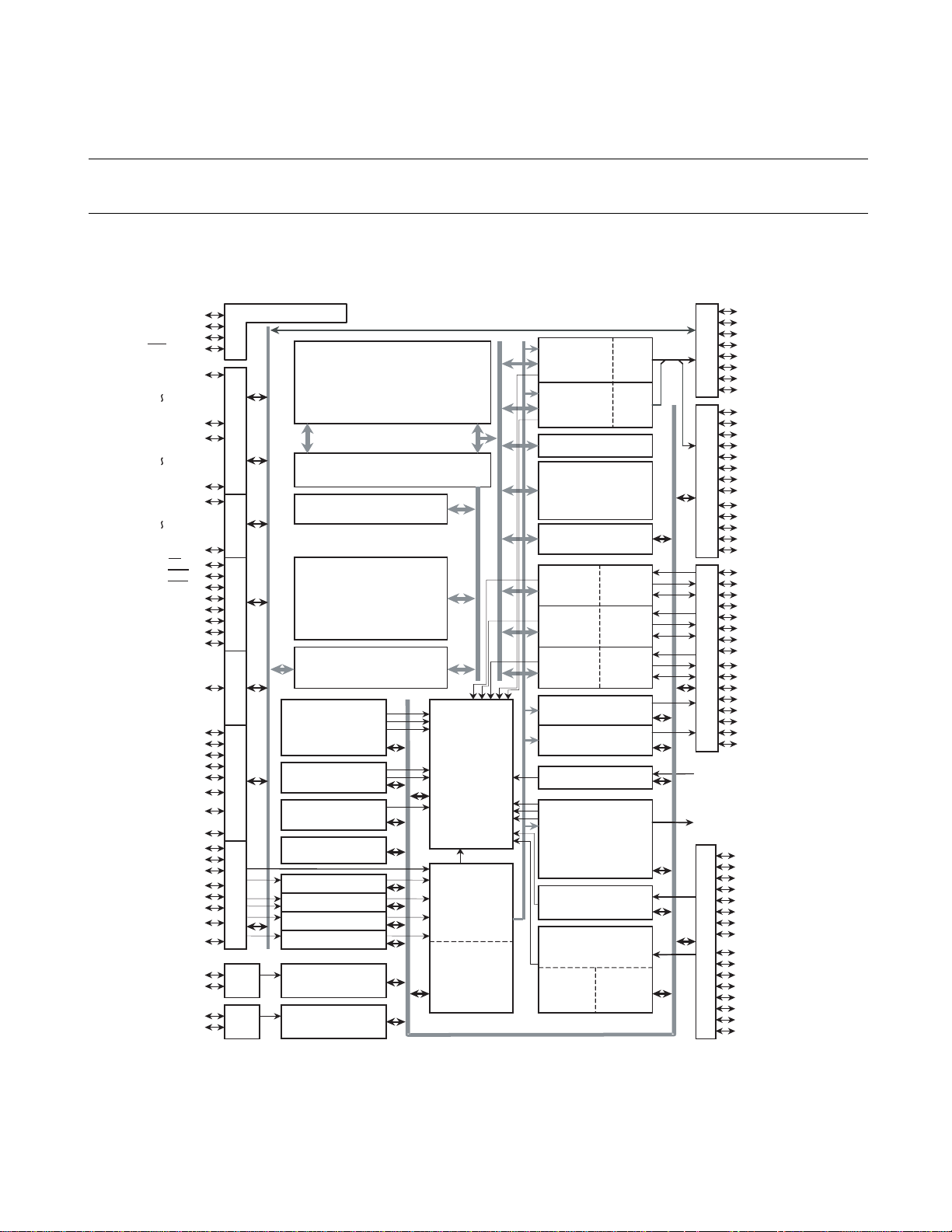
Figure 1.2-1 shows the block diagram of all MB91191/MB91192 series.
■ Block Diagram of All MB91191/MB91192 Series
Figure 1.2-1 Block diagram of all MB91191/MB91192 series
MD0
MD1
MD2
RST
P37/D31
P30/D24
P27/D23
P20/D16
P57/A15
P50/A08
P60/RD
P61/WR0
P62/WR1
P63/ALE
P64
P65
P66/T5O1
P67/T4O
P70/XOUT
P17/RTO 4
P16/RTO 3
P15/RTO 2
P14/RTO 1
P13/RTO 0
P12/EC5/INT1
P11/EC4/INT0
P10/PMSK
P07/EXI 2/PMI
P06/EXI1
P05/EXI 0
P04/CFG
P03/DFG
PO2/DPG
P01/RFG0
P00/RFG1
OSCI
OSCO
XO
X1
Mode Control
P
O
R
T
2
/
3
P
O
R
T
5
P
O
R
T
6
P
O
R
T
7
P
O
R
T
1
P
O
R
T
0
OSC
OSC
FR20 CPU Core
I-bu s D-bus
I-bu s D-bus
RAM 2KB
MB91191R : ROM 254KB
MB91192 : ROM 384KB
MB91F191A: FLASH 254KB
MB91F192 : FLASH 384KB
External Bus CTL
16bit Timer0-3
Interrapt
8/16bit Timer
Controler
16bit Timer4
8bit PWC
CFG
DFG
RFG0
RFG1
fifo
C-unit
29bit x 8
10bit Programale
Prescaler
C-bus
24bit FRC
RAM 256Byte
RAM 64Byte
PPG0
PPG1
Bit Search
MB91191R :RAM 6KB
MB91192 :RAM 8KB
MB91F191A:RAM 6KB
MB91F192 :RAM 8KB
D-bus R-bus
Serial
RAM
128Byte
RAM
128Byte
RAM
128Byte
ch0
Serial
ch1
Serial
ch2
12bit PWM00-02
12bit PWM10-12
External-Interrapt
16bit RTGO-2
External-Interrapt
(Key input)
10bit A/DC
fifo
(soft)
fifo
(hard)
P
O
R
T
4
P
O
R
T
8
/
9
P
O
R
T
C
/
D
INT2-0 (from por t1,D )
RTO4-0 (t o port 1)
P
O
R
T
A
/
B
P47
P46/PPG18
P45/PPG17
P44/PPG16
P43/PPG15
P42/PPG14
P41/PPG13
P40/PPG12
P87/PPG11
P86/PPG10
P85/PPG09
P84/PPG08
P83/PPG07
P82/PPG06
P81/PPG05
P80/PPG04
P94/PPG03
P93/PPG02
P92/PPG01
P91/PPG00
P90/PO
PD0/SI2
PD1/SO2
PD2/SCK 2
PD3/SI1 /INT 2
PD4/SO1
PD5/SCK1
PD6/SCS0
PD7/SI0
PC0/SO0
PC1/SCK0
PC2/PWM 12/SCS1
PC3/PWM11/SCS2
PC4/PWM10
PC5/PWM02
PC6/PWM01
PC7/PWM00
PA7/AN-F/KEY7
PA6/AN-E/KEY6
PA5/AN-D/KEY5
PA4/AN-C/KEY4
PA3/AN-B/KEY3
PA2/AN-A/KEY2
PA1/AN-9 /KEY1
PA0/AN-8 /KEY0
PB7/AN-7
PB6/AN-6
PB5/AN-5
PB4/AN-4
PB3/AN-3
PB2/AN-2
PB1/AN-1
PB0/AN-0
4
Page 19
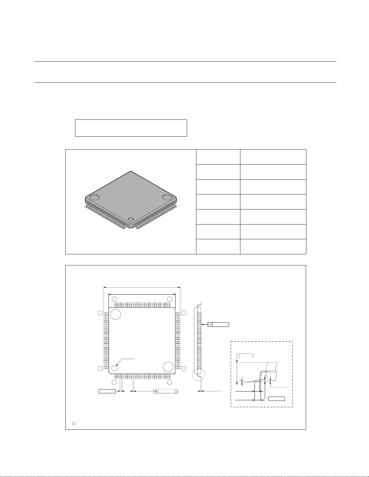
1.3 Package Dimension
120-pin plastic LQFP Lead pitch 0.40 mm
Package width ×
package length
14.0 × 14.0 mm
Lead shape Gullwing
Sealing method Plastic mold
Mounting height 1.70 mm MAX
Weight 0.62 g
Code
(Reference)
P-LFQFP120-14×14-0.40
120-pin plastic LQFP
(FPT-120P-M05)
(FPT-120P-M05)
C
2003 FUJITSU LIMITED F120006S-c-4-5
0.07(.003)
M
INDEX
16.00±0.20(.630±.008)SQ
14.00±0.10(.551±.004)SQ
130
31
6091
120
6190
LEAD No.
(Stand off)
0.10±0.10
(.004±.004)
0.25(.010)
(.024±.006)
0.60±0.15
(.020±.008)
0.50±0.20
(Mounting height)
0~8˚
Details of "A" part
1.50
+0.20
–0.10
+.008
–.004
.059
"A"
0.40(.016)
0.16±0.03
(.006±.001)
0.145±0.055
(.006±.002)
0.08(.003)
*
Dimensions in mm (inches).
Note: The values in parentheses are reference values.
FPT-120P-M05
Note 1)* : These dimensions do not include resin protrusion.
Note 2) Pins width and pins thickness include plating thickness.
Note 3) Pins width do not include tie bar cutting remainder.
MB91191/MB91192 series is available in one type of packages.
■ Package Dimension (LQFP-120)
Figure 1.3-1 Package Dimension of FTP-120-M05
5
Page 20
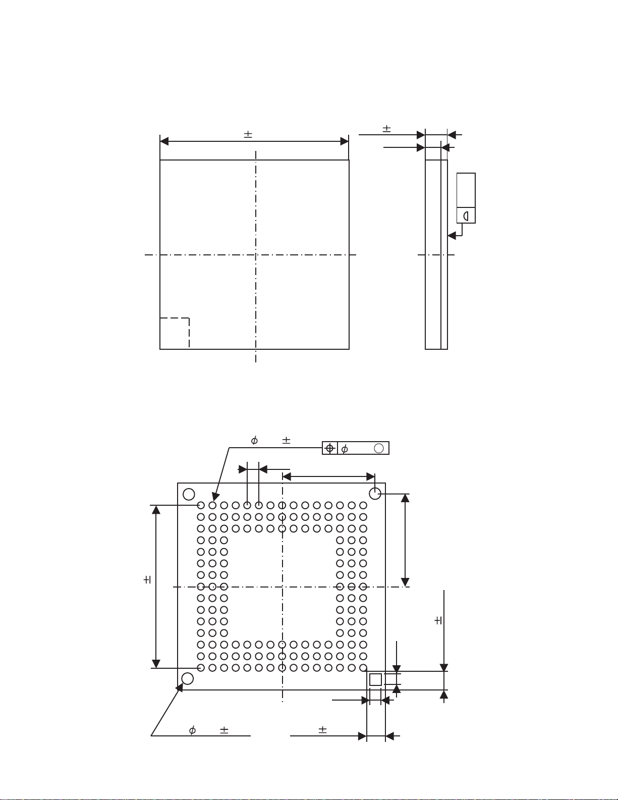
CHAPTER 1 Overview of MB91191/MB91192 Series
0.35 0.05
5
■ Package Dimension (FLGA-144)
Figure 1.3-2 Package dimension of FLGA-144
(INDEX AREA)
11.00
0.05 S Q.
1.10
0.10
(0.80)
0.05
0.05
9.10
3 0.45 0.05
144
0.65
0.755
.175
0.45
0.050
0.08
M
5.175
0.755 0.050
0.45
6
Page 21
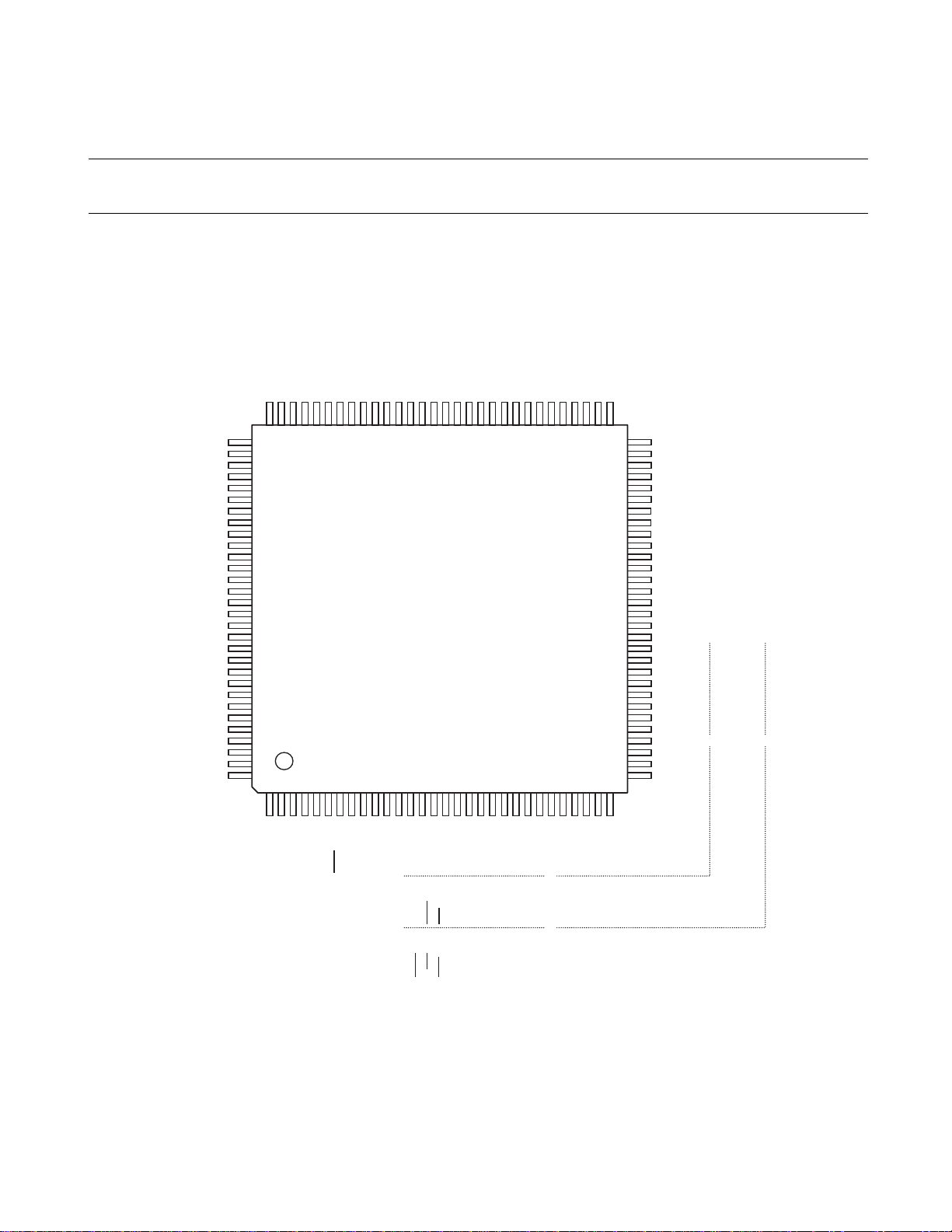
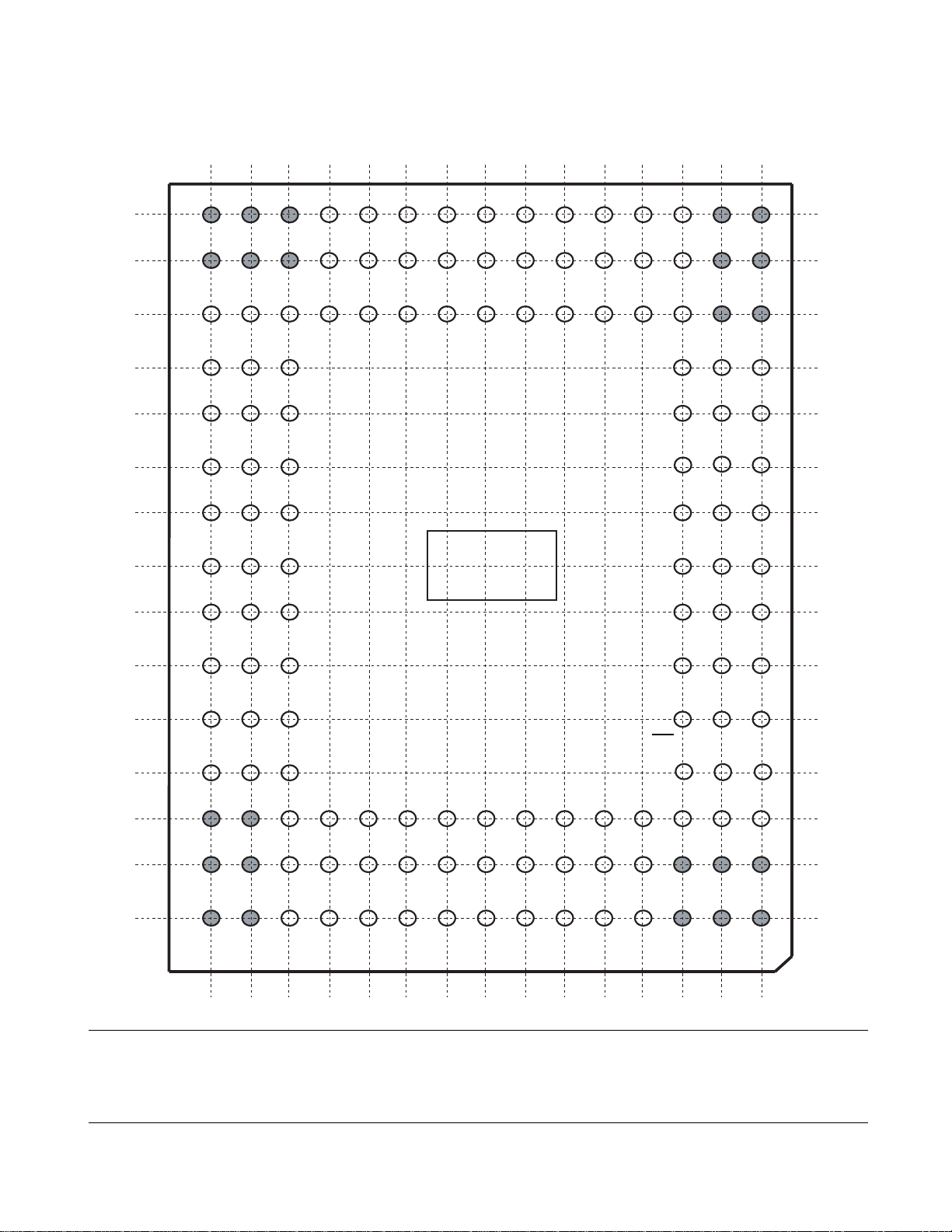
1.4 Pin Assignment
Figure 1.4-1 and Figure 1.4-2 show the pin assignment of the MB91191/MB91192 series.
■ Pin Assignment (LQFP-120)
Figure 1.4-1 Pin assignment of LQFP-120
SS
VDD
PA1/AN-9/KEY1
PA2/AN-A/KEY2
PA3/AN-B/KEY3
PA4/AN-C/KEY4
PA5/AN-D/KEY5
PA6/AN-E/KEY6
PA7/AN-F/KEY7
PD0/SI2
PD1/SO2
PD2/SCK2
PD3/SI1/IN T2
PD4/SO1
PD5/SCK1
PD6/SCS0
PD7/SI0
PC0/SO0
PC1/SCK0
PC2/PWM5/SCS1
PC3/PWM4/SCS2
PC4/PWM3
PC5/PWM2
PC6/PWM1
V
PC7/PWM0
OSCI/PCK
OSCO
P90/PO
P91/PPG00
P92/PPG01
PA0/AN-8/KEY0
PB7/AN-7
PB6/AN-6
PB5/AN-5
PB4/AN-4
PB3/AN-3
PB2/AN-2
PB1/AN-1
PB0/AN-0
AVDD
AVRH
AVSS
V
SS
P17/RTO4
P16/RTO3
P15/RTO2
P14/RTO1
P13/RTO0
P12/EC5/IN T1
P11/EC4/IN T0
P10/PMSK
P07/EXI 2/PMI
P06/EXI1
P05/EXI0
P04/CFG
P03/DFG
P02/DPG
P01/RFG0
P00/RFG1
VDD
95
100
105
110
115
120
90
X0X1MD2
VSS
85
80
75
70
Top View
5
MD1
10
MD0
RST
P70/XOUT
P67/T4O
P66/T5O1
15
P65
P64
P63
P62
P61
20
P60
P20
P21
P22
P23
P24
65
25
P25
P26
P27
VDDP30
60
P93/PPG02
P94/PPG03
P80/PPG04
P81/PPG05
P82/PPG06
55
P83/PPG07
P84/PPG08
P85/PPG09
P86/PPG10
P87/PPG11
50
P40/PPG12
P41/PPG13
P42/PPG14
P43/PPG15
P44/PPG16
45
P45/PPG17
P46/PPG18
P47
P57
P56
40
P55
P54
P53
P52
P51
35
P50
V
SS
P37
P36
P35
30
P31
P32
P33
P34
A15
A14
A13
A12
A11
A10
A09
A08
D31/A07
D30/A06
D29/A05
P57
P56
P55
P54
P53
P52
P51
P50
D31/A15
D30/A14
D29/A13
8bit MPX mode
A00/D24
A01/D25
A02/D26
A03/D27
A08/D24
A09/D25
A10/D26
A11/D27
A04/D28
16bit MPX mode
A12/D28
P25
P26
P20
P21
P22
RD
RD
A00/D16
A01/D17
A02/D18
P23
A03/D19
ALE
P62
WR0
ALE
WR1
WR0
P24
A04/D20
A05/D21
A06/D22
P27
A07/D23
7
Page 22
CHAPTER 1 Overview of MB91191/MB91192 Series
■ Pin Assignment (FLGA-144)
Figure 1.4-2 Pin assignment of FLGA-144
59 56 53 50 47 44 41 38 3 5 32
P94 P82 P85 P40 P43 P46 P56 P53 P 50 P36
58 55 52 4 9 46 45 42 39 36 33
P80 P83 P86 P41 P44 P45 P57 P54 P51 P37
62 63 6 1 60 57 54 51 48 43 40 3 7 34 31
P91 P90 P92 P93 P81 P84 P87 P42 P47 P55 P52 VSS P35
65 66 64 30 28 29
OSCO OSCI VDD P34 P32 P33
68 69 67 27 25 26
PC7 PC6 VSS P31 VDD P30
71 72 70
PC4 PC3
74 75 73 2 1 19 20
PC1 PC0 PC2 P 24 P22 P23
PC5
Top View
77 76 78
PD6 PD7 PD5 P21 P60 P20
22
24
P 27
1 8 16 17
P25
23
P26
Note:
80 7 9 81 1 3 15 14
PD3 PD4 PD2 P 63 P61 P62
83 8 2 84 1 0 12 11
PD0 PD1 PA7 P66 P64 P65
86 85 87 7 9 8
PA5 PA6 PA4 RST P67 P70
89 88 90
PA2 PA3 PA1 MD2 MD0 MD1
91 94 97 100 103 108 111 114 117 120 1 3 2
PA0 PB5 PB2 AVDD P13 P10 P05 P02 VDD X0 VSS X1
93 96 99 102 105 106 109 112 1 15 118
PB6 PB3 PB0 AVSS P16 P15 P12 P07 P04 P01
92 95 98 01 104 107 110 1 13 116 119
PB7 PB4 P B1 AVRH P17 P14 P11 P06 P03 P00
VSS
4 6 5
For the MB91191 series, the FLGA- 144 package does not suppl y. It only supplies for the MB9119 2
series.
8
Page 23

1.5 Pin Function Description
Table 1.5-1 lists the pin function of MB91191/MB91192 series.
The numbers shown in the tables has nothing to do with package pin numbers. For pin
numbers, see "1.4 Pin Assignment".
■ Pin Function List
Table 1.5-1 Pin Function List
Pin No. (LQFP) Pin name Form Function
1 X0(I)
2 X1(O)
3 Vss - It is Vss pin.
4 MD2
5 MD1
6 MD0
7 RST
8
9
10
11 P65 It is general-purpose I/O port. It is CMOS input.
12 P64 It is general-purpose I/O port. It is CMOS input.
13
P70/XOUT
P67/T4O
P66/T5O1 This pin is shared with timer 5 square wave output. It is
P63/ALE/ALE This pin is shared with address strobe output.
A It is crystal oscillation pin.
B
B It is reset input pin. It is CMOS schmitt input.
C
C
It is operating mode specification pin.
It is CMOS schmitt input.
This pin is shared with clock output (X0/2, PCK/2). It is
CMOS input.
This pin is shared with timer 4 square wave output. It is
CMOS input.
CMOS input.
It is CMOS input.
14
15
16
P62/P62/WR1
P61/WR0
P60/RD
/WR0 This pin is shared with write strobe output 0.
/RD This pin is shared with read strobe output.
This pin is shared with write strobe output 1.
It is CMOS input.
It is CMOS input.
It is CMOS input.
9
Page 24

CHAPTER 1 Overview of MB91191/MB91192 Series
Table 1.5-1 Pin Function List
Pin No. (LQFP) Pin name Form Function
17 P20/P20/D16:A00
18 P21/P21/D17:A01
19 P22/P22/D18:A02
20 P23/P23/D19:A03
C
21 P24/P24/D20:A04
It is general-purpose I/O port.
It is CMOS input.
22 P25/P25/D21:A05
23 P26/P26/D22:A06
24 P27/P27/D23:A07
V
25
DD
- It is power supply pin.
26 P30/D24:A00/D24:A08
27 P31/D25:A01/D25:A09
28 P32/D26:A02/D26:A10
29 P33/D27:A03/D27:A11
C
30 P34/D28:A04/D28:A12
It is high-current I/O port and shared with external bus pins.
It is CMOS input.
31 P35/D29:A05/D29:A13
32 P36/D30:A06/D30:A14
33 P37/D31:A07/D31:A15
34 Vss - It is Vss pin.
10
35 P50/A08/P50
36 P51/A09/P51
37 P52/A10/P52
38 P53/A11/P53
39 P54/A12/P54
40 P55/A13/P55
41 P56/A14/P56
42 P57/A15/P57
C
It is high-current I/O port and shared with external bus pins.
It is CMOS input.
Page 25

Table 1.5-1 Pin Function List
Pin No. (LQFP) Pin name Form Function
43 P47
44 P46/PPG18
45 P45/PPG17
46 P44/PPG16
47 P43/PPG15
48 P42/PPG14
49 P41/PPG13
50 P40/PPG12
51 P87/PPG11
52 P86/PPG10
53 P85/PPG09
54 P84/PPG08
55 P83/PPG07
56 P82/PPG06
57 P81/PPG05
C
C
It is general-purpose I/O port. It is CMOS input.
This pin is shared with PPG output.
It is CMOS input.
This pin is shared with PPG output.
It is CMOS input.
58 P80/PPG04
59 P94/PPG03
60 P93/PPG02
61 P92/PPG01
62 P91/PPG00
63
64
P90/PO This pin is shared with general-purpose prescaler output. It is
V
DD
65 OSCO (O)
66 OSCI/PCK(I)
C
C
- It is power supply pin.
A
This pin is shared with PPG output.
It is CMOS input.
This pin is shared with PPG output.
It is CMOS input.
CMOS input.
It is crystal oscillation pin for dedicated general-purpose
prescaler.
67 Vss - It is Vss terminal.
68 PC7/PWM0
69 PC6/PWM1
C
70 PC5/PWM2
This pin is shared with PWM output.
It is CMOS input.
71 PC4/PWM3
11
Page 26

CHAPTER 1 Overview of MB91191/MB91192 Series
Table 1.5-1 Pin Function List
Pin No. (LQFP) Pin name Form Function
72
73
74
75
76
77
78
79
80
81
PC3/PWM4/SCS2
PC2/PWM5/SCS1 This pin is shared with PWM ou tput a nd serial 1 chip select. It
PC1/SCK0 This pin is shared with serial 0 shift clock.
PC0/SO0
PD7/SI0
PD6/SCS0 This pin is shared with serial 0 chip select input.
PD5/SCK1 This pin is shared with serial 1 shift clock.
PD4/SO1
PD3/SI1/INT2
PD2/SCK2 This pin is shared with serial 2 shift clock.
F
C
F
C
F
This pin is shared with PWM output and serial 2 chip select. It
is CMOS schmitt input.
is CMOS schmitt input.
It is CMOS schmitt input.
This pin is shared with serial 0 serial output.
It is CMOS input.
This pin is shared with serial 0 serial input.
It is CMOS schmitt input.
It is CMOS schmitt input.
It is CMOS schmitt input.
This pin is shared with serial 1 serial input.
It is CMOS input.
This pin is shared with serial 1 serial input and external
interrupt 2. It is CMOS schmitt input.
It is CMOS schmitt input.
82
83
84 PA7/AN-F/KEY7
85 PA6/AN-E/KEY6
86 PA5/AN-D/KEY5
87 PA4/AN-C/KEY4
88 PA3/AN-B/KEY3
89 PA2/AN-A/KEY2
90 PA1/AN-9/KEY1
91 PA0/AN-8/KEY0
PD1/SO2
PD0/SI2
C
F
E
This pin is shared with serial 2 serial output.
It is CMOS input.
This pin is shared with serial 2 serial input.
It is CMOS schmitt input.
This pin is shared with analog input and key input.
It is CMOS schmitt input.
12
Page 27

Table 1.5-1 Pin Function List
Pin No. (LQFP) Pin name Form Function
92 PB7/AN-7
93 PB6/AN-6
94 PB5/AN-5
95 PB4/AN-4
D
96 PB3/AN-3
This pin is shared with analog input.
It is CMOS schmitt input.
97 PB2/AN-2
98 PB1/AN-1
99 PB0/AN-0
AV
100
DD
- It is A/D converter power supply pin.
101 AVRH - It is A/D converter reference power supply pin.
102 AVss - It is Vss pin of A/D converter.
103 Vss - It is Vss pin.
104 P17/RTO4
105 P16/RTO3
106 P15/RTO2
C
This pin is shared with RTG output.
It is CMOS input.
107 P14/RTO1
108 P13/RTO0
109
P12/EC5/INT1
This pin is shared with timer 5 clock input and external
interrupt input. It is CMOS schmitt input.
110
111
P11/EC4/INT0 This pin is shared with timer 4 clock input and external
F
interrupt input. It is CMOS schmitt input.
P10/PMSK This pin is shared with PWC mask input.
It is CMOS schmitt input.
13
Page 28

CHAPTER 1 Overview of MB91191/MB91192 Series
Table 1.5-1 Pin Function List
Pin No. (LQFP) Pin name Form Function
112
P07/EXI2/PMI
113 P06/EXI1
114 P05/EXI0
115
116
117
P04/CFG This pin is shared with capstan FG input.
P03/DFG This pin is shared with drum FG input.
P02/DPG This pin is shared with drum pulse input.
118 P01/RFG0
119 P00/RFG1
120
V
DD
This pin is shared with external capture input and PWC input.
It is CMOS schmitt input.
This pin is shared with external capture input.
It is CMOS schmitt input.
It is CMOS schmitt input.
F
It is CMOS schmitt input.
It is CMOS schmitt input.
This pin is shared with reel FG input.
It is CMOS schmitt input.
- It is power supply pin.
14
Page 29
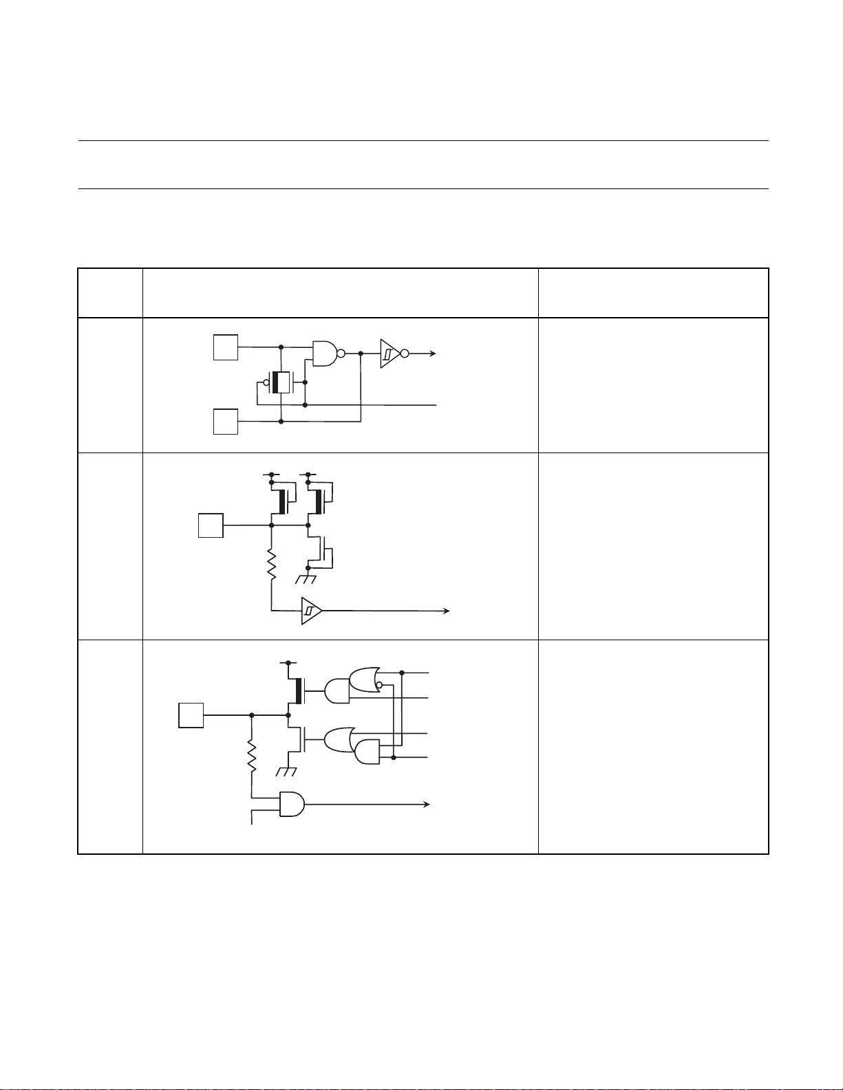
1.6 I/O Circuit Type
Table 1.6-1 shows the I/O circuit type.
■ I/O Circuit Type
Table 1.6-1 I/O circuit types
Classifi-
cation
A
B
X0,OSCI
X1,OSCO
Circuit Type Remark
• Oscillation return resistance about
Clock input
Standby control
1MΩ
• CMOS schmitt inpu t
Input
• CMOS level output
Output data
DC test
• CMOS input without standby
control
C
DC test
Direction CTL
Input
Standby control = 1 fix
15
Page 30

CHAPTER 1 Overview of MB91191/MB91192 Series
Table 1.6-1 I/O circuit types
Classifi-
cation
D
E
Input control
Circuit Type Remark
• CMOS level output
Output data
DC test
DC test
Direction CTL
Analog input
CH selection
Digital input
• CMOS input with input control
• Analog input
• CMOS level output
Output data
DC test
• CMOS schmitt input with input
control
• Analog input
DC test
Direction CTL
F
Input control
Standby control = 1 fix
Analog input
CH selection
Digital input
Output data
DC test
DC test
Direction CTL
Input
• CMOS level output
• CMOS schmitt input without
standby control
16
Page 31

CHAPTER 2
Handling Devices
This chapter describes points to note when using the
MB91191/MB91192 series.
2.1 Precautions When Handling Devices
2.2 Others
17
Page 32

CHAPTER 2 Handling Devices
2.1 Precautions When Handling Devices
The semiconductor device breaks down at a certain probability. Moreover, the failure of
the semiconductor device is greatly controlled by the condition (circuit condition and
environmental condition, etc.) used.
To have the high use, the semiconductor device is explained about reliability about the
matter which should be noted and considered as follows.
■ Precautions when Designing
Here, the matter which should be noted when an electronic equipment is designed with a semiconductor
device is described.
Observance of absolute maximum rating
●
When an excessive stress (voltage, current, and temperature, etc.) adds, the semiconductor device has the
possibility to destroy. The value that this thres hold was provided is an absolute maximum rating. Therefore,
care must be taken not to exceed the rating even for one item.
Observance of recommended operation condition
●
The recommended operation condition is a condition to guarantee normal movement of the semiconductor
device. All standard values for electric features are assured within this condition range. Always u se under
the recommended operation condition. When this condition is exceeded and used, the adverse effect is
occasionally caused for reliability.
Use by the item, the condition, and th e logi cal combinatio n not described t o thi s material is not guaranteed.
Please consult with the section in charge of sales of our company about use by conditions other than being
described for the idea beforehand.
Processing and protection of terminal
●
In the semiconductor device, there are a power supply and various input/output terminals. The followi ng
attention is necessary for these.
• Prevention of over-voltage/over-current
Deterioration is caused in the device when the voltage/current which exceeds the maximum rating is
applied to each terminal, and when it is remarkable, it becomes destruction. Please prevent such an overvoltage/over-current occurring when you design the equipment.
• Protection of output terminal
If the output terminal is short circu ited with the power terminal or other output terminal, or when large
capacity load is connected, a large electrical current may result. If this condition is prolonged, the device
will be damaged, so this kind of connection should not be made.
• Processing of unused input terminal
18
If the input terminal with very high impedance is used while opened, the operation might become unstable.
Ensure connections to the power terminal and ground terminal have the appropriate resistance.
Page 33

Latch up
●
The semiconductor device is composed by the formation of the region of the P-type and the N-type on the
substrate. Internal parasitism PN junction (thyristor structure) might keep doing on-line when the voltage of
an external abnormal voltage is added, and the heavy-current which exceeds hundreds of mA flow to the
power supply terminal. This is called a latch up. The reliability of the device is not only damaged when this
phenomenon occurs but also there is dreading the arrival heat generation, smoking, and the ignition to
destruction. Please note the following points to prevent this.
• There must not be what the voltage more than the maximum rating adds the terminal. Please note
abnormal noise and surge etc.
• An abnormal current must not flow in consideration of the power supply turning on sequence.
Restriction of safety etc. and observance of standard
●
All over the world, various restrictions and standards of safety and the EMI, etc. have been installed. Please
suit these restriction and standard when the customer designs the equipment.
Fail safe design
●
The semiconductor device breaks down at a certain probability. The customer safely designs such as the
device redundancy, fire spreading prevention, exceeding current prevention, and prevention of malfunction
not to occur the injury accident, fire accident, and social damage consequently when the semiconductor
device is broken.
Attention concer nin g usag e
●
The our company semiconductor device is intended to be used for a standard usage (associated equipment
for office appliances such as computers/OA and industries/communications/the measurements and
personal/home equipment etc.). The customer concerns the usage of threatening the life by the breakdown
and malfunction, dreading the damage to the human body, or the special application which the extreme
high reliability is requested (fro aviation/space, atomic control, device for relayed the bottom of the sea,
running control, the medical device to keep the life, etc.), be sure to consult with the sales divisio n of our
company. When you use without the consultation and acknowledge that the responsibility cannot be
assumed about the occurring damage etc.
■ Precautions when Mounting Package
In the package, there are a lead insertion type and a surface mounting type. In both cases, quality assurance
for heat resistance at the soldering stage only applies to the mounting under conditions recommended by us.
Please inquire the section in charge of sales of our company about details of the mounting condition.
Lead insertion type
●
There are two ways to mount the lead insertion type package onto the printing board-the first is to directly
solder it onto the printing board, and the second is to mount it on the printing board using the socket.
When soldering it directly to the printing board, the flow soldering method (wave soldering method)
whereby the solder is melted after inserting the lead through the hole in the printing board is generally used.
In this case, heat stress in excess of the usual maximum rating preservation temperature is added to the lead
part at the soldering stage. Please mount under the mounting recommendation condition of our company.
When the mounting method using the socket is used, if surface processing of the socket contact point and
surface processing of the IC lead are different, contact failure may be generated after a prolonged period.
Therefore, checking the surface processing of the socket contact and surface processing of the IC lead is
recommended before mounting.
19
Page 34

CHAPTER 2 Handling Devices
Surface mounting type
●
The lead used in the surface mounting type package is thinner than that for the insertion type, so its shape is
easily changed. In line with the increased number of pins in the package, the lead pitch is also narrow, and
opening defects due to the lead change and short circuits due to the solder bridge can easily be caused, so
an appropriate mounting technique is required. We recommend the solder re-flow method, and implement
rank classification of the mounting conditions per product. Please mount according to the rank
classification of the our company recommendation.
About keeping the semiconductor device
●
The plastic package is made of resin, so moisture is absorbed if left in a natural environment. When the
heat when mounting on the moisture absorption package joins, the decrease and the package crack of the
wet-proofing by the interfacial flaking off generation might be generated. Please note the following points.
• The be dewy of moisture happens to the product in the place with a rapid temperature change. Store it in
a place with minimum temperature fluctuations that avoid such an environment.
• The depository of the product recommends the use of a dry box. Please keep under the relative humidity
to 70% RH and the temperature to 5 to 30 °C.
• Silica-gel is used as a dry medicine in our company with a damp-proof and high as packing material of
the semiconductor device if necessary an aluminum laminate bag. Put the semiconductor device in the
laminated aluminum bag and close it tightly for storage.
• Please avoid the place where a lot of places and dust where the corrosively gas is generated.
About the baking
●
The moisture absorption package can be dehumidified by executing the baking (heating dryness). Please
execute the baking by the condition which our company recommends.
Static electricity
●
Please note the following points so that the semiconductor device may cause destruction by static electricity
easily.
• Please adjust the relative humidity of th e working environment to 40% to 70% RH. Please examine the
use of TEL device (apparatus for generating ion) etc. if necessary.
• Earth the conveyer, soldering tank and iron, and peripheral incidental equipment to be used.
• In order to prevent electrocution of human body, try to earth through a ring or armlet with high
resistance (about 1MΩ), wear conductive clothing and shoes, and place a conductive mat on the floor to
minimize static build-up.
• Please execute the earth or the electrification prevention to the treatment device and meters.
• Avoid using materials that are easily charged, such as polystyrene foam, to store the assembled board.
20
Page 35

■ Precautions
The reliability of the semiconductor is affected by the peripheral temperature as mentioned before, and
other environmental conditions. Please note the following points.
Humidity
●
As for environment long-term use under the high humidity environment, something wrong with the leak
character might occur in not only the device but also printed wiring board, etc. Please consider the dampproof processing such as giving when the high humidity is assumed.
Static electricity discharge
●
The semiconductor device might cause the malfunction by being generate the electrical discharge in Kon
when electrified thing exists in high voltage near the device. For this case, please treat the prevention of
electrification or the prevention of the electrical discharge.
Corrosively gas, dust, and oil
●
If the device is used within a corrosive gas environment or where dust and oil, etc. may become attached,
the effect may be detrimental due to chemical reactions. Protective measures should be considered when
used under such an environment.
Radiation and cosmic ray
●
A general device does not assume the environment exposed to the radiation and the cosmic ray in the
design. Therefore, use this to shield.
Smoking and ignition
●
The device of the resin molding type is not nonflammability. Do not use the device near any ignitable
substance. In the event of smoke or fire may be generated toxic gases.
Additionally, please consult the section in charge of sales of our company about use under a special
environment for the idea.
21
Page 36

CHAPTER 2 Handling Devices
2.2 Others
The others are explained
■ External Reset Input
When "L" level is input to the RST pin, to ensure the inside ach ieves reset status, "L" level input to the
RST
pin is required for at least five machine cycles.
■ Note on Using External Clock
When using the external clock, drive the X0. Figure 2.2-1 shows the example of using an external clock.
Figure 2.2-1 Example of using an external clock
OPEN
X0
X1
MB91191/MB91192 series
*:Be sure to make X1 pin open.
■ Power Supply Pin
If there are multiple VDD and VSS pins, from the point of view of device design, pins to be of the same
potential are connected the inside of the device to prevent such malfunctioning as latch up. To reduce
unnecessary radiation, prevent malfunctioning of the strobe signal due to the rise of ground level, and
observe the standard for total output current, be sure to connect the V
and ground externally.
Also try to ensure that connection to the V
the power supply source. In addition, We will recommend the ceramic capacitor of about 0.1 µF to be
connected as bypass capacitor between V
■ Crystal Oscillation Circuit
The noise near X0 and the X1 terminal becomes original of the malfunction of this device. The printing
board should be designed so that the X0, X1, crystal oscillator (or ceramic oscillator), and bypass capacitor
to the ground are arranged as close as possible.
Printing board artwork around the X0 and X1 terminals to the ground is strongly recommended, as steady
operation can be expected.
■ Handling NC Pin
Use the Non Connect (N.C.) terminal while open.
■ Mode (MD0 to MD2) Pin
Please tie directly to VDD or VSS and use these terminals.
In order to prevent erroneous entry to test mode due to noise, the pattern length between each mode
terminal and V
at low impedance.
or VSS on the printing board should be as short as possible, and they should be connected
DD
■ At Power On
When the power is turned on, the RST pin must be started from "L" level status, and changed to "H" level
after at least five cycles of the internal operation clock have passed, after the power source reaches the V
level.
and VSS pins to the po wer supp ly
DD
, Vss on this device is at the lowest impedance possible f rom
DD
and VSS near this device.
DD
DD
22
Page 37

CHAPTER 3
CPU
This chapter provides basic explanations for such
elements as the architecture, specifications, and
commands, etc., required to understand the CPU core
functions of the FR series.
3.1 Memory Space
3.2 CPU Architecture
3.3 Dedicated Registers
3.4 General-purpose Register
3.5 Data Construction
3.6 Word Alignment
3.7 Memory Map
3.8 Overview of Instructions
3.9 EIT (Exception, Interruption, and Trap)
3.10 Reset Sequence
3.11 Memory Access Mode
3.12 Clock Generation Section (Low Power Consumption Mechanism)
23
Page 38

CHAPTER 3 CPU
3.1 Memory Space
The logical address space of the FR20 series is 4 Gbytes (232 addresses), and the CPU
performs linear access.
■ Direct Addressing Area
The under-mentioned area of the address space is used for I/O. This area is called the "direct addressing
area" and operand addresses can be specified directly within the command. A direct area is different as
follows depending on the size of the accessed data.
• Byte data access:0-0FF
• Half word data access:0-1FF
• Word data access:0-3FF
■ Memory Map
Figure 3.1-1 shows the memory map of the MB91191/MB91192.
H
H
H
24
Page 39

Figure 3.1-1 MB91191/MB91192 Memory Map
00000000
000001FF
00000200
000002FF
00000300
0000037F
00000380
000003BF
000003C0
000003FF
00000400
000007FF
00000800
00000FFF
00001000
0000107F
00001080
000010FF
00001100
0000E7FF
0000E800
0000FFFF
00010000
000BFFFF
000C0000
000C07FF
000C0800
000FFFFB
000FFFFC
00100000
FFFFFFFF
H
H
H
PPG0 Data RAM area 256byte
H
H
I/O area
SIO0 Data RAM area 128byte
H
H
PPG1 Data RAM area 64byte
H
H
I/O area
H
H
H
H
I/O area
Access interdiction
H
H
SIO1 Data RAM area 128byte
H
H
SIO2 Data RAM area 128byte
H
H
Access interdiction
H
H
Internal RAM area 6Kbyte
H
H
Access interdiction
H
H
Internal RAM
H
H
Internal ROM
H
Reset vector
H
H
area 2Kbyte
area (254kByte)
External expansion area
H
MB91191R MB91192
Direct
Access
Area
1KB
Initial vector area
I/O area
PPG0 Data RAM area 256byte
SIO0 Data RAM area 128byte
PPG1 Data RAM area 64byte
I/O area
I/O area
Access interdiction
SIO1 Data RAM area 128byte
SIO2 Data RAM area 128byte
Access interdiction
Internal RAM area 8Kbyte
Access interdiction
Internal RAM
area 2Kbyte
Access interdiction
Internal ROM
area (384kByte)
Reset vector
External expansion area
00000000
000001FF
00000200
000002FF
00000300
0000037F
00000380
000003BF
000003C0
000003FF
00000400
000007FF
00000800
00000FFF
00001000
0000107F
00001080
000010FF
00001100
0000DFFF
0000E000
0000FFFF
00010000
0007FFFF
00080000
000807FF
00080800
0009FFFF
000A0000
000FFFFB
000FFFFC
00100000
FFFFFFFF
H
H
H
H
H
H
H
H
H
H
H
H
H
H
H
H
H
H
H
H
H
H
H
H
H
H
H
H
H
H
H
H
H
Note:
Under single-chip mode, access to the external extension area is impossible.
Select internal RO M external bus mode using the mode register to access the external exte nsion
area.
25
Page 40

CHAPTER 3 CPU
3.2 CPU Architecture
The FR20 CPU is a high performance core that adopts highly functional commands for
the embedded application as well as RISC architecture.
■ Feature of CPU Architecture
Adoption of RISC architecture
●
• Basic instruction: one instruction one cycle
32 bit architecture
●
• General-purpose register 32 bits × 16
Linear memory space of 4 GB
●
Installing of multipliers
●
• 32 bits x multiplication 32 bits: 5 cycles
• 16 bits x multiplication 16 bits: 3 cycles
Reinforcement of interruption processing function
●
• High-speed response speed (6 cycles)
• Support for multiple interr up ts
• Lev el mask function (16 levels)
Reinforcement of instruction for I/O operation
●
• Memory memory transfer operation
• Bit processing instruction
High code efficiency
●
• 16 bits in basic instruction word length
Low power consumption
●
• Sleep mode, stop mode
■ Construction of Internal Architecture
The FR20 CPU adopts the Harvard architecture structure whereby the command bus and data bus are
independent.
26
The on chip command cache is connected to the command bus (T-bus). A 32-bit <--> 16-bit bus converter
is connected to the data bus (D-bus), and performed interfaces between the CPU and peripheral resources.
A Harvard <--> Princeton bus converter is connected to both the I-bus and D-bus, performed and interfaces
between the CPU and bus controller.
Page 41

Figure 3.2-1 shows the construction of internal architecture.
Figure 3.2-1 Construction of Internal architecture
FR20 CPU
D-BUS I-BUS
Instruction
Cache
32bit
16bit
Bus converter
R-bus C-bus
Harvard
Princeton
Bus converter
●
Resource
CPU
Bus controller
The FR20's 32-bit RISC architecture is compactly implemented on the CPU. A five-level command
pipeline method is adopted to execute one command per cycle. The pipeline is composed of the following
stages.
• Instruction fetch (IF): The instruction address is output, and the instruction is fetched.
• Instruction decode (ID): The decode does the fetched instruction. The register is read.
• Execution (EX): The operation is executed.
• Memory access (MA): Loading into the memory or the store is accessed.
• Write-back (WB): Writes th e operation results (or loaded memory data) to the register.
Figure 3.2-2 shows the instruction pipeline.
Figure 3.2-2 Instruction pipeline
CLK
Instruction 1 WB
Instruction 2 MA
Instruction 3 EX
Instruction 4 ID
Instruction 5 IF
Instruction 6
WB
MA
EX
ID
IF
WB
MA
EX
ID
WB
MA
EX
WB
MA
WB
The instruction is never in any order executed. Accordingly, if command A enters the pipeline before
command B, command A always reaches write backstage before command B.
As a rule, the instruction is executed at the speed of one instruction per cycle. However, a number of cycles
27
Page 42

CHAPTER 3 CPU
are required to execute commands for the load/store command to which memory wait is attached, branch
commands that do not have delay slots, and multi -cycle commands. Also, when the supplied instruction is
slow, the execution speed of the instruction decrease.
Refer to "3.8 Overview of Instructions" for details.
32-bit ↔ 16-bit bus converter
●
Interfaces between the D-BUS that quickly accesses at 32-bit width and the R-BUS that accesses at 16-bit
width, and realizes data access from the CPU to built-in peripheral circuit.
When 32-bit width access is performed from the CPU, this bus converter accesses the R-BUS by
converting it to 16-bit width access twice. Some of built-in peripheral circuits have access width-related
restrictions.
Harvard ↔ Princeton bus converter
●
Coordinates between the CPU command access and data access, and realizes smooth interface with the
external bus.
In CPU, the instruction bus and the data bus are the independent Harvard architecture structures. On the
other hand, the bus controller that controls the external bus has a Princeton architectural structure with a
single bus. This bus converter ranks the priority order for command access and data access of the CPU, and
controls access to the bus controller. This operation always optimizes the external bus access ranking.
It also has a two-word write buffer to eliminate CPU bus waiting time and a one-word pre-fetch buffer to
fetch commands.
28
Page 43

3.3 Dedicated Registers
Use the dedicated registers for specified purposes. Program counter (PC), program
status (PS), tabl e base register (TBR), return pointer (RP), system stack pointer (SSP),
user stack pointer (USP), and multiplication/division results registers (MDH/MDL) are
prepared.
■ Dedicated Registers List
Figure 3.3-1 shows the dedicated register list.
Figure 3.3-1 Dedicated registers list
Program counter (PC)
Program status (PS) ILM SCR CCR
Table base register (TBR)
Return pointer (RP)
System stack pointer (SSP)
User stack pointer (USP)
Multiplication and division result register
(MDH)
(MDL)
■ Program Counter (PC)
Function of program counter (PC: Program Counter) is described.
The program counter (PC) consists of 32-bit.
Figure 3.3-2 shows the bit configuration of the program counter (PC).
Figure 3.3-2 Program counter (PC)
bit
The address of the executed instruction is shown with the program counter.
If the PC is updated when an i nstruction is execute d, Bit 0 is set to "0". B it 0 ma y be "1 " only when an odd
address is specified as the branch destination address.
Even in that case, bit 0 is invalid, and the command must be placed in the address of the multiple of two.
The initial value by reset is irregular.
31 0 Initial value
■ Program Status Register (PS)
This register retains the program status, and is separated into three parts, namely, ILM, SCR, and CCR.
Refer to "3.3.1 Program Status Register (PS)" for details.
The undefined bits are all reserved bits. When the register is read, "0" is always read. Writing is invalid.
XXXXXXXX
H
29
Page 44

CHAPTER 3 CPU
■ Table Base Register (TBR)
Function of table base register (TBR : Table Base Register) is described .
The table base register (TBR) consists of 32-bit.
Figure 3.3-3 shows the bit configuration of the table base register (TBR).
Figure 3.3-3 Table base register (TBR)
bit
31 0 Initial value
The table base register retains the starting address of the vector table used for EIT processing.
The initial value by reset is 000FFC00
■ Return Pointer (RP)
Function of Return Pointer (RP: Return Pointer) is described.
The return pointer (RP) consists of 32-bit.
Figure 3.3-4 shows the bit configuration of the return pointer (RP).
bit
31 0 Initial value
The address which returns from the sub routine is maintained at the return poin ter.
The value of PC is forwarded to this RP at CALL instruction execution time.
The content of RP is forwarded to PC at RET instruction execution time.
The initial value by reset is irregular.
■ System Stack Pointer (SSP)
Function of system stack poi nter (SSP: System Stack Pointer) is descr ibed.
The system stack pointer (SSP) consists of 32-bit.
.
H
Figure 3.3-4 Return pointer (RP)
000FFC00
H
XXXXXXXXH
30
Figure 3.3-5 shows the bit configuration of the system stack pointer (SSP).
Figure 3.3-5 System stack pointer (SSP)
bit
31 0 Initial value
00000000
H
SSP is the system stack pointer.
When the S flag is "0", the SSP functions as R15. The SSP can be specified explicitly.
Also used as the stack pointer specifying the stack that saves the PS and PC when EIT occurs.
The initial value by reset is 00000000
.
H
Page 45

■ User Stack Pointer (USP)
Function of user stack pointer (USP: User Stack Pointer) is described.
The user stack pointer (USP) consists of 32-bit.
Figure 3.3-6 shows the bit configuration of the user stack pointer (USP).
Figure 3.3-6 User stack pointer (USP)
bit
USP is the user stack pointer.
When the S flag is "1", the USP functions as R15. The USP can be s pecified explicitly . The initial v alue by
reset is irregular.
The USP cannot be used for the RETI instruction.
31 0 Initial value
■ Multiplication and Division Result Register (MDH/MDL)
Function of multiplication and division result register (MDH/MDL: Multiply & Divide register) is
described.
The multiplication and division result register (MDH/MDL) consists of 32-bit.
Figure 3.3-7 shows the bit configuration of the multiplication and division result register (MDH/MDL).
Figure 3.3-7 Multiplication and division result storage register (MDH/MDL)
bit
MDH
MDL
MDH and MDL are the multiplication and division register. Each register is 32-bit long.
The initial value by reset is irregular.
31 0
XXXXXXXX
Initial value
XXXXXXXX
XXXXXXXXH
H
H
Functions when multiplication is executed
●
In the case of 32-bit x 32-bit multiplication, the 64-bit long operation results are stored in the
multiplication/division results register in the following format.
• MDH: Higher 32-bit
• MDL: Lower 32-bit
In the case of 16-bit x 16-bit multiplication, the results are stored in the multiplication/division results
register as follows.
• MDH: Indeterminate
• MDL: 32-bit
Functions when division is executed
●
When beginning to calculate, the dividend is stored in MDL.
When division is calculated using the DIV0S/DIV0U, DIV1, DIV2, DIV3, or DIV4S commands, the
results are stored in the MDL and MDH as follows.
• MDH: surplus
• MDL: commerce
31
Page 46

CHAPTER 3 CPU
3.3.1 Program Status Register (PS)
The register retains the program status, and is separated into three parts, ILM, SCR, and
CCR.
A bit undefined in figure is reservation all bit. When the register is read, "0" is always
read. Writing is invalid.
■ Program Status Register (PS)
Figure 3.3-8 shows the configuration of the program status register (PS).
Figure 3.3-8 Program status register (PS)
bit
Condition code register (CCR)
●
Figure 3.3-9 shows the configuration of the condition code register (CCR).
bit
The function of each bit is explained as follow.
[bit5] S: Stack flag
This bit specifies the stack pointer to be used as R15.
Value Function
31 20 16 10 8 7 0
7 6 5 4 3 2 1 0 Initial value
S I N Z V C --00XXXX
0
ILM
Figure 3.3-9 Condition code register (CCR)
The system stack pointer (SSP) is used as R15. When the EIT occurs, this bit is
automatically set to "0". (Note t hat a value saved on the stack is the value before it is
cleared)
SCR
CCR
H
32
1 The user stack pointer (USP) is used as R15.
This bit is cleared to "0" by a reset.
Select the SSP when the RETI instruction is executed.
Page 47

[bit4] I: Interrupt enable flag
Permission and the interdiction of the user interruption demand are controlled.
Value Function
User interruption interdiction.
0
When the INT instruction is executed, this bit is cleared to "0".
(Note that a value saved on the stack is the value before it is cleared)
1
This bit is cleared to "0" by a reset.
[bit3] N: Negative flag
This bit indicates the code when the operation results are defined as integers expressed as complements
of 2.
Value Function
0 It is indicated that operation result was a positive value.
1 It is indicated that operation result was a negative value.
Initial state by reset is irregular.
[bit2] Z: Zero flag
This bit indicates whether or not the operation result is 0.
Value Function
0 It is indicated that operation result was the values other than 0.
User interruption permission.
Mask processing of user interrupt requests is controlled by the value retained by ILM.
1 It is shown that operation result was 0.
Initial state by reset is irregular.
[bit1] V: Overflow flag
This bit is considered to be the integer expressing the operand used for operations as complements of 2,
and indicates whether or not an overflow was generated as the result of such operation.
Value Function
0 It is indicated that no overflow has occurred as a result of the operation.
1 It is indicated that an overflow has occurred as a result of the operation.
Initial state by reset is irregular.
33
Page 48

CHAPTER 3 CPU
[bit0] C: carrying flag
System Condition code Register (SCR)
●
Figure 3.3-10 shows the configuration of the system condition code register (SCR: System Condition Code
Register).
This bit indicates whether or not carry or borrow was generated from the highest bit through the
operation.
Value Function
0 It is indicated that no carry or borrow has occurred.
1 It is indicated that a carry or borrow has occurred.
Initial state by reset is irregular.
Figure 3.3-10 System condition code register (SCR)
bit
10 9 8 Initial value
D1 D0 T XX0
H
Each bit function of the system condition code register (SCR) is explained as follows.
[bit10, 9] D1, D0: Flag for step division
The middle data of step division execution time is maintained. Do not change while executing the
division processing.
Restart of the step division is guaranteed by saving/returning the PS register value when other processes
are carried out during the step division. Initial state by reset is irregular.
When the DIV0S instruction is executed, the divided and the divisor are referenced and set.
When the DIV0U instruction is executed, the bits clear forcibly.
[bit8] T: step trace trap flag
It is a flag which specifies whether to make the step trace trap effective.
Value Function
0 Step trace trap invalidity
1
Step trace trap effective
In this case, all NMIs for user and user interrupts will be interrupt disabled.
34
This bit is initialized to "0" by a reset.
The emulator uses the function of the step trace trap. When the emulator is used, it cannot be used in user
program.
Page 49

Interrupt level mask register (ILM)
●
Figure 3.3-11 shows the configuration of the interrupt level mask register (ILM).
Figure 3.3-11 Interrupt level register (ILM)
bit
20 19 18 17 16 Initial value
ILM4 ILM3 ILM2 ILM1 ILM0 01111
H
The interrupt level mask register (ILM) retains the interrup t level mask value, and values retained by this
ILM are used as the level mask.
Interrupt requests are received only when the supported interrupt level is higher than the level indicated by
this ILM out of the interrupt requests to be input to the CPU.
As for the level value, 0(00000
) is the strongest, and 31(11111B) is weakest.
B
There is a limitation in the value which can be set from the program.
If the original value is between 16 to 31, the new value must be between 16 to 31. When the command
setting 0 to 15 is executed, the value (specified value + 16) is transferred.
If the original value is between 0 to 15, an arbitrary value between 0 to 31 can be set.
This register is initialized to 15 (01111
) by a reset.
B
35
Page 50

CHAPTER 3 CPU
3.4 General-purpose Register
Register R0 to R15 is a general-purpose register. These registers are used as the
pointer for memory access and accumulator for various operations.
■ General-purpose Register
Figure 3.4-1 shows the configuration of the general-purpose register.
Figure 3.4-1 Configuration of general-purpose register
32
R0
XXXX XXXX
R1
XXXX XXXX
R12
R13
R14
R15
bit
[Initial value]
XXXX XXXX
XXXX XXXX
AC
FP
SP
XXXX XXXX
0000 0000
H
H
H
H
H
H
Register R0-R15 is a general register. These registers are used as the pointer for memory access and
accumulator for various operations. The following of the 16 registers are expected to have special uses, so
some commands are emphasized.
• R13: Virtual accumulator (AC)
• R14: Frame pointer (FP)
• R15: Stack pointers (SP)
R0 to R14 of the initial value by reset is irregular. R15 becomes 00000000
(value of SSP).
H
36
Page 51

3.5 Data Construction
B
The data allocation of the FR20 series uses as follow.
• Bit ordering: Little endian
• Byte ordering: Big endian
■ Bit Ordering
In the FR20 series, the little endian has been adopted as a bit ordering.
Figure 3.5-1 shows the data allocation of the bit ordering.
Figure 3.5-1 Data allocation of bit ordering
bit
31 30 29 28 27 26 25 24 23 22 21 20 19 18 17 16 15 14 13 12 11 10 9 8 7 6 5 4 3 2 1 0
MSB
■ Byte Ordering
Big endian is adopted as the byte ordering for the FR family.
Figure 3.5-2 shows the data allocation of the byte ordering.
(n+1) address 11001100
(n+2) address 11111111
(n+3) address 00010001
LS
Figure 3.5-2 Data allocation of byte ordering
MSB LSB
Memory bitNo.31 23 15 7 0
10101010 11001100 11111111 00010001
bit
70
n address 10101010
37
Page 52

CHAPTER 3 CPU
3.6 Word Alignment
As commands and data are accessed per byte, addresses to be allocated differ
depending on the command length and data width.
■ Program Access
It is necessary to arrange the program of the FR20 series in the address of the multiple of two. Bit 0 of the
program counter (PC) is set to "0" when updating the PC in line with execution of the com mand. It may be
"1" only when an odd address is specified as the branch destination address. Even in that case, bit 0 is
invalid, and the command must be placed in the address of the multiple of two.
There is no odd number address exception.
■ Data Access
In the FR20 series, when data is accessed, forced alignment is applied to the address depending on its width
as follows.
• Word Access: An address must be a multiple of 4. (The lowest 2-bit is forcibly "00".)
• Half-word access: An address must be a multiple of 2. (The lowest bit is forcibly "0".)
• Byte Access: -
When word or half-word data is accessed, "0" is forcibly set to some bits, which are the calculation results
of the effective address. For example, in the @(R13,Ri) addressing mode, the register before addition is
used for calculations as it is (even tho ugh the lowest bit is 1), and th e lower bits of th e addition results will
be masked. A register before calculation is not masked.
(example) LD @(R13,R 2),R0
R13 00002222
R2 00000003
Addition result 00002225
Address pin 00002224
H
H
H
Lower 2-bit forcibly mask
H
38
Page 53

3.7 Memory Map
The memory map for the FR20 series is shown.
■ Memory Map
The address space of the memory is 32 bit linear.
Figure 3.7-1 shows the memory map.
Figure 3.7-1 Memory map
0000 0000
0000 0100
0000 0200
0000 0400
000F FC00
000F FFFF
FFFF FFFF
H
H
H
H
H
H
H
Byte data
Halfword data
Word data
Vector table
initial region
Direct addressing region
Direct addressing
●
The under-mentioned region of the address space is a region for I/O. In this area, the operand address can
be specified directly within the command through direct addressing.
The size of the address area which an address can be directly specified is different in each data length.
• Byte data: (8 bits): 0 to 0FF
• Half-word data: (16 bits): 0 to 1FF
• Word data: (32 bits): 0 to 3FF
Vector table initial region
●
The region of 000FFC00
The vector table used for EIT processing can be allocated to an arbitrary address by rewriting the TBR, but
it is allocated to this address on initialization through reset.
H
H
H
- 000FFFFFH is EITT vector table initial area.
H
39
Page 54

CHAPTER 3 CPU
3.8 Overview of Instructions
The FR20 series supports logical operation and bit operations that are optimized for
embedded application, and direct addressing commands as well as a general RISC
command system. The set list shows the appendix. As each command is 16 bits length
(some commands are 32 or 48 bits), memory usage is more efficient.
■ Overview of Instructions
The instruction set can be divided into the following function groups.
• Arithmetic operation
• Load and store
•Divergence
• Logical operation and bit operation
• Direct addressing
•Others
Arithmetic operation
●
It has standard arithmetic operation commands (addition, subtraction, comparison) and shift commands
(logic shift, arithmetic operation shift). Operations with carry that are us ed for multi-word length operations
and operations that do not change the flag value which are convenient for address calculations are enabled
for addition and subtraction.
Furthermore, it has 32-bit x 32-bit and 16-bit x 16-bit multip lication commands, and the 32-bit/3 2-bit step
division commands.
Also equipped with an immediate transfer command that sets immediate values to the register, and an interregister transfer command.
The arithmetic operation command executes all operations using a general-purpose register and
multiplication/division register within the CPU.
Load and store
●
Load and store are the commands that read and write to external memories. They are also used to read and
write the peripheral circuits (I/O) within the chip.
Load and store have three types of access length, namely byte, half-word, and word. In addition to normal
indirect register memory addressing, memory addressing is also possible for certain commands such as
indirect displacement registers and indirect increment/decrement registers.
40
●
Branch
In the FR20 series, whether the operations are with or without delay slots can be specified for the branch
command.
It is an instruction of the branch, the call, the interruption, and the return. There are two types of branch
command. One type has a delay slot and the other does not. They can be optimized to suit the purpose.
Refer to "3.8.1 Branch Command with Delay Slot" and "3.8.2 Branch Command without Delay Slot" for
Page 55

details of the branch commands.
Logical operation and bit operation
●
Logic operation instruction can perform AND, OR, and EOR logic operations between general-purpose
registers, or between a general-purpose register and the memory (or I/O). Moreover, the bit operation
instruction can operate the content of the memory (And, I/O) directly. The register of the memory
addressing is generally indirect.
Direct addressing
●
Direct addressing commands are used to access between I/O and general-purpose registers, or between I/O
and the memory. The I/O address can be accessed quickly and efficiently by direct specification within the
command instead of indirect register. Indirect memory addressing to the register with register increment/
decrement is also enabled for some commands.
Others
●
This command executes flag set up within the PS register, stack operation, code/zero expansion, etc. Also
equipped with high-level language supported function entry/exit, and register multi-load/store commands.
41
Page 56

CHAPTER 3 CPU
3.8.1 Branch Command with Delay Slot
The operation with the delay slot branches prior to execute the command at the branch
destination after executing the command located immediately after the branch
command.
■ Branch Command with Delay Slot
The following commands execute the branch command with delay slot.
JMP:D @Ri CALL:Dlabel12 CALL:D @Ri RET:D
BRA:D label9 BNO:D label9 BEQ:D label9 BNE:D label9
BC:D label9 BNC:D label9 BN:D label9 BP:D label9
BV:D label9 BNV:D label9 BLT:D label9 BGE:D label9
BLE:D lab el9 BGT:D label9 BLS:D label9 BHI:D label9
■ Operation of Branch Command with Delay Slot
Operations with delay slots branch out after executing the command placed just after the branch command
(called a "delay slot") prior to execute the branch destination command.
As the delay slot command is executed before the branch operation, the apparent execution speed is 1
cycle. The NOP command must be placed as an alternative if an effective command cannot be inserted in
the delay slot.
[example]
; Row of instruction
ADD R1, R2 ;
BRA:D LABEL ; Branch instructio ns
MOV R2, R3 ; Delay slot ......Executed before branch
...
LABEL:STR 3 and @R4 ; The divergence ahead
The command placed in the delay slot is executed whether the branch condition for the condition branch
command will be realized or not.
For delay branch commands, the execution order of the partial command seems to be reversed, but this
applies only to PC update operations, and other operations (i.e. update and refer to register) are absolutely
executed in the described order.
Concrete examples are shown below.
The Ri to be referred to the JMP:D@Ri/CALL:D@Ri command will not be effected even if the command
●
within the delay slot updates the Ri.
42
[example]
LDI:32 #Label, R0
JMP:D @R0 ; Branches out to Label
LDI:8 #0, R0 ; No effects on the branch destination address
...
Page 57

The RP to be referred by the RET:D command will not be effected even if the command within the delay
●
slot updates the RP.
[example]
RET:D ; Branch to address defined beforehand in RP
MOV R8, RP; No effect on the return operation
...
The flag referred by the Bcc: Drel command is not effected by the delay slot command either.
●
[example]
ADD #1, R0; Flag change
BC:D Overflow ; Branch to execution result of above instruction
ANDCCR #0 ; Do not refer to this flag update in the above-mentioned branch instruction.
...
When RP is referred to for the command within the delay slot under the CALL:D command, the updated
●
contents will be read by the CALL:D command.
[example]
CALL:D Label ; Update RP and branch
MOV RP and R0 ; RP of an execution above-mentioned CALL:D result is forwarded.
..
■ Limitations for Branch Command with Delay
Instruction that can be placed in the delay slot
●
Only commands that satisfy the following conditions can be executed within the delay slot.
• 1 cycle instruction.
• No branch instruction.
• Inst ruction which does not influence operation even when order chang es
The "1-cycle command" is a command in which "1", "a", "b", "c", or "d" is described in the cycle number
column within the commands list.
Step trace trap
●
Step trace trap will not be generated between execution of the branch command with delay slot and the
delay slot.
Interrupt/NMI
●
No interrupt/NUM is received between execution of the branch command with delay slot and the delay slot.
Undefined instruction exception
●
If an undefined command exists with the delay slot, undefined command exception will not be generated.
At this time, undefined instruction operates as NOP instruction.
43
Page 58

CHAPTER 3 CPU
3.8.2 Branch Command without Delay Slot
Branch Command without Delay Slot is described.
■ Branch Command without Delay Slot
The following commands execute the branch command without delay slot.
JMP @Ri CALL label12 CALL @Ri RET
BRA label9 BNO label9 BEQ label9 BNE label9
BC label9 BNC label9 BN label9 BP label9
BV label9 BNV label9 BLT label9 BGE label9
BLE label9 BGT label9 BLS label9 BHI label9
■ Operation of Branch Command without Delay Slot
Operation of ones without delay slots are absolutely executed in command rank order. The instruction
provided immediately before the branch instruction is not executed after branching.
[example]
; Row of instruction
ADD R1, R2 ;
BRA LABEL ; Branch instruction (delay slot none)
MOV R2, R3 ; Not executed
...
LABEL:STR 3 and @R4 ; The branch ahead
Execution cycle number for branch commands without delay slots will be 2 cycles branched, or 1 cycle
non-branched. As the appropriate command cannot be inserted into the delay slot, the command code
efficiency is better than the branch command with the delay slot described the NOP instruction. A balance
between execution speed and code efficiency can be struck by selecting either the operation with the delay
slot when effective commands can be set in the delay slot, or the operat ion without the delay slot when
effective commands cannot be set.
44
Page 59

3.9 EIT (Exception, Interruption, and Trap)
EIT indicates suspension of program execution due to generation of an event while
executing the current and other programs. It is a general term for Exception, Interrupt,
and Trap.
■ EIT (Exception, Interruption, and Trap)
The exception is an incident which occurs in relation to the context under execution. Execution restarts
from the instruction that caused the exception.
The interruption is an incident which occurs without any relation to the context under execution. The event
factor is hardware.
The trap is an incident which occurs in relation to the context under execution. There is something directed
by the program like the system call. Execution restarts from the instruction following the one that caused
the trap.
■ EIT Factor
The EIT factors are as follow.
• Reset
• User interruption (internal resource and exter nal interruption)
•NMI
• Delayed interrupt
• Undefined instruction exception
• Trap instruction (INT)
• Trap instruction (INTE)
• Step trace trap
• Coprocessor absent trap
• Coprocessor error trap
■ Return from EIT
Use the RETI instruction to return from EIT.
45
Page 60

CHAPTER 3 CPU
3.9.1 Interrupt Level of EIT
Interrupt levels is controlled by 0 to 31 by five bits.
■ Interrupt level of EIT
The allocation of each level is as follow.
Table 3.9-1 Interrupt level
Interrupt level
2 decimal
number
00000 0
00001 1
00010 2
00011 3
00100 4 INTE instruction, step trace trap
00101 to
01110
01111 15 NMI (for user)
10000 to
11110
11111 31 - When ICR is set, it is an interruption interdiction.
10 decimal
number
5 to 14 (System reservation)
16 to 30 Interrupt
It is a level of 16 to 31 that the operation is possible.
Undefined command exception, coprocessor absence trap, coprocessor error trap and INT instruction are
unaffected by the interrupt level. Moreover, ILM is occasionally changed.
Factor Remark
(System reservation)
When the original value of the ILM is 16 to 31,
values within this range cannot be set as the ILM
by the program.
When ILM is set, it is a user interruption
interdiction.
■ Level Mask to Interruption/NMI
When NMI and interrupt requests are generated, the interrupt l evel held by the interru pt factor is compared
with the level mask value held by the ILM. And, when the following condition consists, the mask is done,
and the demand is not accepted.
Interrupt level held by factor ≥ Level mask value
46
Page 61
3.9.2 Interrupt Stack Operation
The value of PC and PS is saved and revived in the area shown by SSP. After an
interrupt, PC is stored in the address indicated by the SSP, and PS is stored in the
address (SSP+4).
■ Interrupt Stack
Figure 3.9-1 shows the example of the interrupt stack.
Figure 3.9-1 Interrupt stack operation diagram
[Example] [Befor interrupt] [After interrupt]
SSP SSP
80000000
H
Memory
80000000
H
7FFFFFFC
7FFFFFF8
H
H
80000000
7FFFFFFC
7FFFFFF8
7FFFFFF8
H
H
H
H
PS
PC
47
Page 62

CHAPTER 3 CPU
3.9.3 EIT Vector Table
From address which TBR shows to vector region for EIT region of 1KB
■ EIT Vector Table
Each vector is 4 bytes, and the relationship between the vector number and vector address is expressed
below.
vctadr = TBR + vctofs = TBR +(03FCH - 4 × vct)
vctadr: Vector Address
vctofs: Vector offset
vct: Vector number
The lowest 2-bit of the addition result are always handled as "00".
The area of 000FFC00
to 000FFFFFH is an initial area of the vector table by reset. A special function is
H
allocated partially of the vector. The vector table on the architecture is shown in Table 3.9-2 .
Table 3.9-2 Vector table
Vector number Vector Address Description
0 00
1 01
2 02
3 03
4 04
5 05
6 06
7 07
8 08
9 09
10 0A
11 0B
12 0C
13 0D
14 0E
15 0F
16 10
17 to
63
64 40
65 41
66 to
255
11
42
3F
FF
H
H
H
H
H
H
H
H
H
H
H
H
H
H
H
H
H
to
H
H
H
H
to
H
H
000FFFFC
TBR + 03F8
TBR + 03F4
TBR + 03F0
TBR + 03EC
TBR + 03E8
TBR + 03E4
TBR + 03E0
TBR + 03DC
TBR + 03D8
TBR + 03D4
TBR + 03D0
TBR + 03CC
TBR + 03C8
TBR + 03C4
TBR + 03C0
TBR + 03BC
H
H
H
H
H
H
H
H
H
H
H
H
H
H
H
H
H
TBR + 03B8H to
TBR + 0300
TBR + 02FC
TBR + 02F8
H
H
H
TBR + 02F4H to
TBR + 0000
H
Reset
System reservation
System reservation
System reservation
System reservation
System reservation
System reservation
Coprocessor absent trap
Coprocessor error trap
INTE Instruction
Instruction break exception
Operand break trap
Step trace trap
System reservation
Undefined instruction exception
NMI (for user)
Mask enable interrupt factor #0 (IRQ0)
Mask enable interrupt factor #1 (IRQ2) to
Mask enable interrupt factor #47 (IRQ47)
System reservation (used for REAL OS)
System reservation (used for REAL OS)
INT Instruction
48
Page 63

3.9.4 Multiple EIT Processing
When a number of EIT factors are generated simultaneously, one of the EIT factors is
selected and accepted in the CPU, and after the EIT sequence is executed, such EIT
factors are detected again. This operation is repeated as necessary.
When EIT factors are detected, if there are no more EIT factors that can be accepted, the
handler command for the last EIT factor accepted will be executed.
Therefore, the handler order for each factor when a number of EIT factors are generated
simultaneously is determined by the following two elements.
• Priority level of EIT factor acceptance
• How to mask the other fact or at receiving
■ Priority Level of EIT Factor Acceptance
Priority for acceptance of the EIT factors indicates the order when selecting the factors executing the EIT
sequence that saves PS and PC, updates the PC (on demand) and performs mask processing of other
factors. The handler of the factor previously accepted is not always executed first.
Table 3.9-3 shows the priority level of the EIT factor acceptance.
Table 3.9-3 Priority level of EIT factor acceptance and masking other factor
Priority order
of acceptance
1 Reset Other factors are abandoned.
2 Undefined instruction exception Cancellation
3
4 User Interrupt ILM = Level of accepted factor
5 NMI (for user) ILM=15
7 INTE Instruction ILM=4
8 Step trace trap ILM=4
A tinge of mask processing onto other factors after accepting the EIT factors is added, and each handling
procedure for the generated EIT factors are also mentioned in Table 3.9-4 .
Coprocessor absent trap
Coprocessor error trap
Factor Masking of other factor
INT Instruction I Flag=0
None
49
Page 64

CHAPTER 3 CPU
Table 3.9-4 Execution sequence of EIT handler
Execution sequence of handler Factor
1
Reset
*1
2 Undefined instruction exception
3
4
Step trace trap
INTE instruction
*2
*2
5 NMI (for user)
6 INT instruction
7 User interrupt
Coprocessor absent trap
8
Coprocessor error trap
*1: Other factors are abandoned.
*2: If the INTE instruction is executed in steps, only EIT of the step trace trap generates
INTE instruction.
The factor by INTE is disregarded.
Figure 3.9-2 shows the example of multiple EIT processing.
Figure 3.9-2 Example of multiple EIT processing
[Example]
Priority level
(High) NMI generation
(Low) INT instruction execute
Main routine
NMI handler
INT instruction handler
First execute
Next execute
50
Page 65

3.9.5 Operation of EIT
This section explains operation of EIT
■ Operation of EIT
As per the following explanation, the "PC" at the transfer origin indicates the address of the command that
detected each EIT factor.
The "following command address" means that the command that detected EIT is as follows.
• If LDI is 32: PC+6
• If LDI: 20 and COPOP, COPLD, C OPST and used: PC+4
• Other instructions: PC+2
Operation of user interruption/NMI
●
When a user interrupt or interrupt request of NMI for user is generated, the request is accepted or not is
determined in the following order.
Right or wrong judgment of interruption demand acceptance
●
1. The interruption levels of request s that are gener ated simultaneously are compared, and the one with the
highest level (the smallest numeric value) will be selected. In terms of the levels used for comparisons,
the value retained by the supported ICR is used for mask enable interrupts, and a predetermined constant
is used for NMI.
2. When a number of interrupt requests of the same level are generated, the one with the youngest interrupt
number is selected.
3. Compares the interrupt level wit h the se lected inter rupt request with th e level m ask va lue determin ed by
ILM.
When the interrupt level is greater th an or equal to the level mask value, the int errupt request is masked
and not accepted.
To (4) at interrupt levels < level mask value.
4. When the selected interruption request is an interr uption that can be masked, the interruption request
will be masked and will not be accepted when the I flag is 0. If the I flag is 1, go to 5). When the
selected interrupt request is NMI, go to 5) regardless of the I-flag value.
5. When the above condition occurs, the interrupt request is accepted at the command-processing gap.
When an EIT request is detected, if the user interrupt/NMI request is accepted, the CPU operates as follows
using the interrupt number supporting the accepted interrupt request. ( ) in the [operation] shows the
address which the register indicates.
51
Page 66

CHAPTER 3 CPU
[Operation]
1. SSP-4 → SSP
2. PS → (SSP)
3. SSP-4 → SSP
4. Address of the following instruction→(SSP)
5. Interrupt level of accepted request→ ILM
6. "0" → S Flag
7. (TBR + Vector offset of accepted interrupt request)→ PC
Prior to execute the front command of th e handler after the interrupt sequence ends, a new EIT is detected.
At this stage, if an acceptable EIT is generated, the CPU transits to the EIT processing sequence.
■ Operation of INT Instruction
The INT #u8 instruction operates as follow.
Branch to the interrupt handler for the vector indicated by u8.
[Operation]
1. SSP-4 → SSP
2. PS → (SSP)
3. SSP-4 → SSP
4. PC+2 → (SSP)
5. "0" → I Flag
6. "0" → S Flag
7. (TBR+3FCH - 4 × u8)→ PC
■ Operation of INT Instruction
The INT instruction operates as follow.
Branch to the interrupt handler for the vector indicated by vector number #9.
[Operation]
1. SSP-4 → SSP
2. PS → (SSP)
3. SSP-4 → SSP
4. PC+2 → (SSP)
5. "00100" → ILM
6. "0" → S Flag
7. (TBR+3D8H)→ PC
Do not use the INTE instruction during the INTE ins truction and step trace trap processing routine.
Moreover, EIT is not generated while executing the step by INTE.
52
Page 67

■ Operation of Step Trace Trap
When the T flag of the SCR within the PS is set, and the step trace function is set to Enabled, a trap is
generated per command execution and creates a break.
Condition of step trace trap detection
●
•T Flag = 1
• There is no delayed branch instructio n.
• While executing other than the INTE command and step trace trap processing routine.
When the above condition occurs, breaks at the command operation gap.
[Operation]
1. SSP-4 → SSP
2. PS → (SSP)
3. SSP-4 → SSP
4. Address of the following instruction→(SSP)
5. "00100" → ILM
6. "0" → S Flag
7. (TBR+3CCH)→ PC
When step trace traps are enabled by setting the T flag, NMI for users and user interruption are disabled.
Moreover, EIT by the INTE instruction is not generated.
■ Operation of Undefined Instruction Exception
If an undefined instruction is detected when decoding the command, an undefined instruction exception is
generated.
Detection condition of undefined instruction exception
●
• 1) It is detected that it is undefined instru ctio n at the decoding of the instruction.
• 2) Placed outside the delay slot (not immediately after the delay branch command).
When the above condition occurs, an undefined instruction exception is generated, and a break is created.
[Operation]
1. SSP-4 → SSP
2. PS → (SSP)
3. SSP-4 → SSP
4. PC → (SSP)
5. "0" → S Flag
6. (TBR+3C4H)→ PC
The address of the actual command that detected the undefined instruction exception is saved as the PC.
53
Page 68

CHAPTER 3 CPU
■ Coprocessor Absent Trap
When a coprocessor command using an unmounted coprocessor is executed, a coprocessor absence trap is
generated.
[Operation]
1. SSP-4 → SSP
2. PS → (SSP)
3. SSP-4 → SSP
4. Address of the following instruction→(SSP)
5. "0" → S Flag
6. (TBR+3E0H)→ PC
■ Coprocessor Error Trap
If an error occurs while using a coprocessor, when the coprocessor command that operates the coprocessor
is executed next, a coprocessor error trap is generated.
[Operation]
1. SSP-4 → SSP
2. PS → (SSP)
3. SSP-4 → SSP
4. Address of the following instruction→(SSP)
5. "0" → S Flag
6. (TBR+3DCH)→ PC
Note:
This product does not contain the coprocessor.
■ Operation of RETI Instruction
The RETI instruction is an instruction which returns from EIT processing routine.
[Operation]
1. (R15) → PC
2. R15+4 → R15
3. (R15) → PS
4. R15+4 → R15
Care must be taken that the stack pointer to be referred to returning of the PS and PC is selected in
accordance with the S flag contents. When the command that operates R15 (stack pointer) within the
interrupt handler is executed, set the S flag to "1" and use the USP as R15. The S flag must be returned to
"0" before the RETI command.
■ Delay Slot
54
In the delay slot of the branch instruction, there is a restriction concerning EIT.
Refer to "3.8.1 Branch Command with Delay Slot" for details.
Page 69

3.10 Reset Sequence
This section explains the reset when the CPU is the operation state.
■ Reset Factor
The reset factor is as follow.
• Input from external reset pin
• Software reset by the SRST bit operation of the standby control register (STCR)
• Count up of watchdog timer
•Power on reset
■ Initialization by Reset
The reset factor is generated, the CPU is initialized.
Releasing from the external reset pin or software reset
●
• The pin is set to the predetermined state.
• Each resource in the device is put in the reset state. The control register is initialized to the
predetermined value.
• The lowest gear is selected for the clock.
■ Reset Sequence
When a reset factor is released, the CPU executes the following reset sequence.
• (000FFFFC
Note:
After reset, operation mode needs to be set by the mode register setting.
) → PC
H
55
Page 70

CHAPTER 3 CPU
3.11 Memory Access Mode
In the FR20 series, operation mode is controlled by the mode pins (MD2, 1, 0) and the
mode register (MODR).
■ Operation Mode
In the operation mode, there are a bus mode and an access mode.
Bus mode Access mode
Single-chip
Bus Mode
●
Internal ROM
external bus
External ROM
external bus
32 - bit bus widht
16 - bit bus widht
8 - bit bus widht
The bus mode controls the internal ROM operation and external access function operation, and is specified
by the mode set up pins (MD2, 1, 0) and M1, M0 bit of the mode register (MODR).
Access mode
●
The access mode controls the external data bus width, and is specified by the mode set up pins (MD2, 1, 0)
and BW1, 0 bits within the AMD0/AM D1/AMD32/AMD4 and AMD5 (address mode registe rs).
■ Mode Pin
Operation is specified by three pins (MD2, 1, 0) as per Table 3.11-1 .
Table 3.11-1 Mode Pin and setting mode
Mode pin
Mode name
MD2 MD1 MD0
0 0 0
0 0 1
0 1 0
External
vector mode 0
External
vector mode 1
External
vector mode 2
Reset vector
access area
External 8 bits
External 16 bit
External 32 bit
External data bus
width
Remark
The use of the terminal
is prohibited.
0 1 1
1 - - - - -
56
Internal vector
mode
Internal (Mode register) Single-chip mode
The use of the terminal
is prohibited.
Page 71

■ Mode Data
Data that the CPU writes at "0000 07FFH" after reset is called mode data.
The mode register (MODR) exists in "0000 07FF
under the set up mode of this register. The mode register can be written only once after resetting.
The set value of this register is valid immediately after writing.
■ Mode Register (MODR)
bit
Initial value
Address: 0000 07FF
Access
[bit7, 6]: M1, M0
Table 3.11-2 Bus mode setting bits and function
M1 M0 Function Remark
0 0 Single-chip mode
0 1 Internal ROM external bus mode
H M1 M0 XXXXXXXXB
WW
There are bus mode setting bits. These bits specify the bus mode after writing the mode register.
" and after setting to this register, operation is carried out
H
Figure 3.11-1 Mode register (MODR)
76543210
Bus mode setting mode
Note:
1 0 External ROM external bus mode Setting disabled
1 1 - Setting disabled
Only set the "00" and "01" for this product above.
[bit5-0]:System Reserved bit
Always write "0" to these bits.
57
Page 72

CHAPTER 3 CPU
■ Notes on Writing to Mode Register (MODR)
Before writing to the MODR, AMD0 to AMD5 must be set, and the bus width in each chip select (CS) area
must be decided.
The MODR has no bits used to set the bus width.
For the bus width, before writing to the MODR, the mode pins (MD2 to 0) are valid. After MODR writing,
set values (BW1, BW0) of the AMD0 to AMD5 will be valid.
For example, the external reset vector performs in the normal area 0 (the area in which the CSOX is active),
but in this case, the bus width is decided by the MD2 to MD0 pi ns . The bus width at that time is set to 32 or
16 bits by MD2 to MD0, and if MODR is written while nothing is set to AMD0, the initial value of the
AMD0 bus width has been set to 8 bits. So bus operation will be performed by transiting the area 0 to 8 bit
bus mode after writing the MODR, and erroneous operation will result.
AMD0 to AMD5 must be set before writing the MODR to prevent this kind of problem.
Figure 3.11-2 Notes on writing to mode register (MODR)
RST (Reset)
MODR programming
Bus width setting: MD2, 1, 0 BW1, 0 of MD0-5A
58
Page 73

3.12 Clock Generation Section (Low Power Consumption Mechanism)
The clock generation section is the modules that have the following functions:
• CPU clock generation (including the gear function)
• Peripheral clock generation (including the gear function)
• Reset generation and cause retention
• Standby function
• Built-in PLL (duty correction circuit)
■ Register in Clock Generation Section
Figure 3.12-1 Register in Clock Generation Section
bit
Address: 000480H
000481H
000482H
000483H
000484H
000485H
17
RSRR/WTCR Reset Factor/Watchdog Cycle Control Register
STCR Standby Control Register
Reserve (Access interdiction)
CTBR Timebase Timer Clear Register
GCR Gear Control Register
WPR Watchdog Reset Generation Dalayed Register
59
Page 74

CHAPTER 3 CPU
■ Block Diagram of Clock Generation Section
Figure 3.12-2 Block Diagram of Clock Generation Sec tion
X0
X1
Oscillation
circuit
Internal interrupt
Internal reset
R-bus
[Gear control unit]
GCR register
1/ 2
PLL
[Stop/Sleep control unit]
STCR regiter
[Reset factor circuit]
CPU gear
Peripheral
gear
M
P
X
State
transition
control
circuit
Internal
clock
generation
circuit
Reset
generation
F/F
CPU clock
Internal bus clock
Internal peripheral clock
STOP state
SLEEP state
CPU hold request
Internal reset
Power-on detection
RST pin
RSRR register
[Watchdog control unit]
WPR register
CTBR register
Watchdog F/F
Timebase timer
Count
clok
60
Page 75

3.12.1 Reset Factor Register (RSRR) and Watchdog Timer Cycle
Control Register (WTCR)
The reset factor register (RSRR) retains reset types generated, and the watchdog timer
cycle control register (WTCR) specifies the cycle for the watchdog timer.
■ Reset Factor Register (RSRR) and Watchdog Timer Cycle Control Register (WTCR)
Figure 3.12-3 Reset factor register (RSRR) and watchdog timer cycle control register (WTCR)
Initial value after
Power ON
Address: 000480
Access
[bit7]: PONR
When this bit is "1", it indicates that the previo usly generated reset was a powe r-on reset. When t his bit
is "1", contents other than this bit of this register are invalid.
[bit6]: (Reserved)
It is reserved bit. The reading value is undefined.
[bit5]: WDOG
bit
H
76543210
PONR WDOG ERST SRST WT1 WT0 1XXX XXXXB
R RRR WW
When this bit is "1", it indicates that the previously generated reset was a watchdog reset.
[bit4]: ERST
When this bit is "1", it indicates that the previously generated reset was caused by the external reset pin.
[bit3]: SRST
When this bit is "1", it indicates that the previously generated reset was caused by the s oftware reset
request.
[bit2]: (Reserved)
It is reserved bit. The reading value is undefined.
[bit1, 0]: WT1, 0
These bits specify the cycle of the watchdog timer. The bits and the selected cycle have the following
relationship. These bits are initialized when the entire reset is generated.
61
Page 76

CHAPTER 3 CPU
Table 3.12-1 Watchdog timer cycle specified by WT1 and WT0
WT1 WT0
0 0
0 1
1 0
1 1
Note: φ is twice as large as X0 when GCR CHC is 1, and is one time as large as X0 when GCR CHC is 0.
Writing spacing to at least necessary for
control generation of watchdog reset WPR
15
φ × 2
(Initial value) φ × 2 15 to φ × 2
17
φ × 2
19
φ × 2
21
φ × 2
φ × 2 21 to φ × 2
Timer from last 5A
write to WPR to
H
occurrence of watchdog resettin g
16
φ × 2
φ × 2
17
to φ × 2
19
to φ × 2
18
20
22
62
Page 77

3.12.2 Standby Control Register (STCR)
This register controls standby operations and specifies the oscillation stabilization wait
time.
■ Standby Control Register (STCR)
Figure 3.12-4 Standby control register (STCR)
bit
7 6 5 4 3 2 1 0
Address: 00000481
Access
[bit7]:STOP
When "1" is written to this bit, the status will be stop that stops the internal peripheral clock, the internal
CPU clock, and oscillation.
[bit6]:SLEP
When "1" is written to this bit, the status will be standby that stops the internal CPU clock. If "1" is
written to both the STOP bit and this bit, the STOP bit is handled as the priority, so the status will be
stop.
H
STOP SLEEP SRST OSC1 OSC0
R/W R/W R/W R/W R/W
Initial value
000111--
B
[bit5]:(Reserved)
[bit4]:SRST
When "0" is written to this bit, a software reset request is generated.
[bit3, 2]:OSC1, 0
These bits specify the oscillation stabilization wait time. These bits and selected cycle have the
following relationship. This bit is initialized by a power-on reset, an d is unaffected by any other rese t
factors.
Table 3.12-2 Oscillation stabilization wait time specified by OSC1 and OSC0
OSC1 OSC0 Oscillation Stabilization Wait Time
0 0
0 1
1 0
1 1
φ × 2
15
φ × 2
17
φ × 2
19
φ × 2
21
(Initial value)
Note: φ is twice as large as X0 when GCR CHC is 1, and is one time as large as X0 when GCR CHC is 0.
[bit1, 0]:(Reserved)
There are reserved bits. The reading value is undefined.
63
Page 78

CHAPTER 3 CPU
3.12.3 Timebase Timer Clear Register (CTBR)
This register initializes the timebase timer contents to 0.
■ Timebase Timer Clear Register (CTBR)
Figure 3.12-5 Timebase timer clear register (CTBR)
Note:
bit
Address: 000483
Access
76543210
D7 D6 D5 D4 D3 D2 D1 D0 XXXX XXXXB
H
WWWWWWWW
Initial value
[bit7 to 0]
Writing A5
, 5AH continuously to this register clears the timebase timer to 0 immediately after 5AH.
H
The reading value of this register is irregular. There is no restriction on the time interval between A5
and 5AH writing.
Clearing the timebase timer using this register temporarily fluctuates oscillation stability wait interval,
watchdog cycle, and peripheral cycles that use the timebase.
H
64
Page 79

3.12.4 Gear Control Register (GCR)
The gear control register controls the gear functions of the CPU and peripheral clocks.
■ Gear Control Register (GCR)
Figure 3.12-6 Gear Control Register (GCR)
bit
Address: 000484
Access
[bit7, 6]:C CK1, 0
These bits specify the CPU gear cycle. The bits and selected cycles have the following relationship.
These bits are initialized by a reset.
Table 3.12-3 CPU machine clock
CCK1 CCK0 CHC
76543210
CCK1 CCK0 PCK1 PCK0 CHC 11--11-1B
H
R/W R/W R/W R/W R/W
CPU machine clock
(source oscillation: input frequency from X0)
0 0 0 Source oscillation × 1
0 1 0 Source oscillation × 1/2
1 0 0 Source oscillation × 1/4
1 1 0 Source oscillation × 1/8
0 0 1 Source oscillation × 1/2
0 1 1 Source oscillation × 1/2 × 1/2
1 0 1 Source oscillation × 1/2 × 1/4
Initial value
1 1 1 Source oscillation × 1/2 × 1/8 (Initial value)
65
Page 80

CHAPTER 3 CPU
[bit3, 2]:PCK1, 0
Table 3.12-4 Peripheral machine clock
These bits specify the peripheral gear cycle. The bits and the selected cycles have the following
relationship. These bits are initialized by a reset.
PCK1 PCK0 CHC
0 0 0 Source oscillation × 1
0 1 0 Source oscillation × 1/2
1 0 0 Source oscillation × 1/4
1 1 0 Source oscillation × 1/8
0 0 1 Source oscillation × 1/2
0 1 1 Source oscillation × 1/2 × 1/2
1 0 1 Source oscillation × 1/2 × 1/4
1 1 1 Source oscillation × 1/2 × 1/8 (Initial value)
[bit0]:CHC
This bit selects whether 1/2 division cycle or PLL/DCC cycle of the oscillation circuit is used as the
basic clock. The setting "1" is the 1/2 division cycle and the setting "0" is the PLL/DCC cycle.
(source oscillation: input frequency from X0)
Peripheral machine clock
66
Page 81

3.12.5 Watchdog Reset Generation Delay Register (WPR)
This register clears the flip-flop for the watchdog timer. Using this register postpones
generation of the watchdog reset.
■ Watchdog Reset Generation Delay Register (WPR)
Figure 3.12-7 Watchdog reset generation delay register (WPR)
bit
764543210
Address: 000485
Access
D7 D6 D5 D4 D3 D2 D1 D0 XXXX XXXXB
H
WWWWWWWW
[bit7 to 0]
Writing A5
immediately after 5A
, 5AH continuously to this register clears the flip-flop for the watchdog timer to "0"
H
, and postpones generation of the watchdog reset.
H
The reading value of this register is irregular. There is no time limit between A5
writing both data is not finished within the period as per the following table, a watchdog reset is
generated. However, clearing is automatically carried out under stop/sleep mode, so when these
conditions are generated, the watchdog reset is automatically post poned.
Table 3.12-5 Watchdog timer cycle specified by WT1 and WT2
WT1 WT0
Writing spacing to at least
necessary for control generation of
Time from 5A
watchdog reset WPR
0 0
0 1
1 0
φ × 2
φ × 2
φ × 2
15
17
19
final writing in WPR to
H
generation of watchdog reset
φ × 2
φ × 2
φ × 2
15
to φ × 2
17
to φ × 2
19
to φ × 2
16
18
20
Initial value
and 5AH, but if
H
1 1
Note: φ is twice as large as X0 when GCR CHC is 1, and is one time as large as X0 when GCR CHC is 0.
φ × 2
21
φ × 2
21
to φ × 2
22
67
Page 82

CHAPTER 3 CPU
3.12.6 Reset Factor Retention
The reset factor retention holds the factor of previous generation. All flag is cleared to
"0" by reading.
Once a factor flag is set, it is not cleared unless the factor is read.
■ Block Diagram of Reset Factor Retention Circuit
Figure 3.12-8 Reset factor circuit Block Diagram
Power-on
detection
watch-dog Timer
reset detect Circuit
RST pin
Reset input circuit ERST
■ Setting of Reset Factor Retention
No special settings are required to use the rest factor function. Commands for reading the reset factor
register and branching to the appropriate program shall be placed near the front of the program to be set in
the reset entry address.
[example]
State
transition
circuit
PONR
WDOG
ERST
SRST
decoder
.or.
Internal bus
PONR
WDOG
SRST
SRST
68
RESET-ENTRY
LDI:32 #RSRR,R10
LDI:8 #10000000B,R2
LDUB @R10,R1 ; GET RSRR VALUE INTO R1
MOV R1,R10 ; R10 USED AS A TEMPORARY REGISTER
AND R2,R10 ; WAS PONR RESET?
BNE PONR-RESET
LSR #1,R2 ; POINT NEXT BIT
MOV R1,R10 ; R10 USED AS A TEMPORARY REGISTER
AND R2,R10 ; WAS WATCH DOG RESET?
BNE WDOG-RESET
...
Page 83

Notes:
• When the PONR bit is 1, contents of bits other than that should be handled as indeterminate. Thus, if a
reset factor needs to be checked, the command for checking the power-on reset must be placed at the
front.
• Checking reset factors other than power-on reset can be done in any position. Priorities are determined
in the order of checking.
69
Page 84
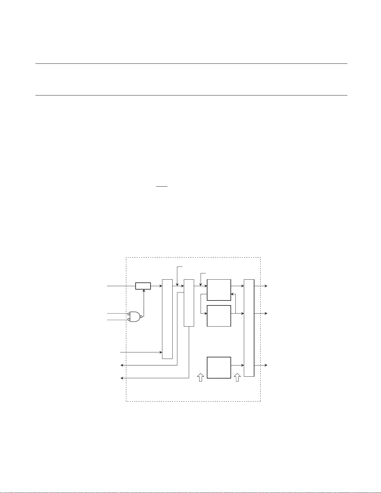
CHAPTER 3 CPU
3.12.7 Stop Status
Stop status indicates the status that stops all internal clocks and oscillation circuit
operation. It can be minimized the power consumption.
■ Overview of Stop Status
Stop status indicates the status that stops all internal clocks and oscillation circuit operation. It can be
minimized the power consumption.
Transition to the stop status is performed as follow.
• Writing in standby control register ( STCR) using the instruction
Returning from the stop status is performed one of the following.
• Inte rrupt reque st (only appl ies to periphe rals where interrupt request can be generated even under stop
status)
• Applying the L level to the RST
Under stop status, all internal clock s are stopped, so bu ilt-in peripherals other than those that can generate
interrupts for returning will be stopped.
pin
■ Block Diagram of Stop Control Section
Figure 3.12-9 shows the block diagram of stop control section.
Figure 3.12-9 Block diagram of stop control section
STCR
Internal bus
Internal Interrupt
Internal reset
CPU Hold Enable
CPU Hold Request
STOP state display singal
STOP
Clear
State transition control circuit
STOP state transition request signal
Stop signal
State decoder
Clock
generation
Internal
bus clock
generation
Internal
peripheral
clock
generation
Clok stop
request singal
Internal clock generation circuit
Clok cancel
request singal
CPU clock
Internal bus clock
Internal peripheral clock
70
Page 85

■ Transition to Stop Status
Transition to the stop state using an instruction
●
Write "1" to bit 7 of the STCR register to enter stop status.
After a stop request is issued, the status is changed such that the CPU does not use the internal bus, and
then the clocks are stopped in the following order.
CPU clock →internal bus clock → internal peripheral clock
The oscillation circuit stops when the internal peripheral clock stops.
Notes:
The following routine must be used to change the status to stop using a command.
• Before writing to the STCR, set the s ame value to the CCK1, 0 and PCK1, 0 bit lots of the GCR, and the
gear ratios between the CPU system clock and peripheral system clock should be the same.
• Do not provide the stop state when the CHC bit of GCR is "0". To enter stop status, "1" must be set to
the CHC bit of the GCR, and 1/2 division system clock must be selected.
• At least five consecutive NOP instructions must be provided immediately after writing to the STCR.
[Setting]
DI:8 #00000001b,R1 ; CPU=Peripheral gear ratio, CHC=1
LDI:32 #GCR,R2
STB R1,@R2
LDI:8 #10010000b,R1 ; STOP=1
LDI:32 #STCR,R2
STB R1,@R2
NOP ;
NOP ;
NOP ;
NOP ;
NOP ;
■ Return by Stop Status
Returning from stop status can be performed by generating an interrupt or reset.
Return by interrupt
●
If the interrupt-enabled bit attached to the peripheral function is valid, returns from the stop status by
generating a peripheral interrupt.
Returning from the stop status to the normal operation status is carried out in the following procedure.
Generates interrupt -> Restarts oscillation circu it operation -> Waits for oscillation stabilization -> After
stabilization, restarts supply of internal peripheral clock -> Restarts supply of internal bus clock -> Restarts
supply of internal CPU clock
The program execution after oscillation stabilization waiting time is as follows.
• When the level of the interrupt is enabled by the I flag of CPU ILM
71
Page 86

CHAPTER 3 CPU
• When the level of the interrupt is disabled by the I flag of CPU ILM
Return by RST pin
●
Returning from stop status to normal operating status is as per the following procedure.
- After saving the register, fetches in the interrupt vector and executes from the processing routine.
- Executes the instruction the following instruction that changed to the stop s tatu s.
Notes:
L level application to the RST
Waits for oscillation stabilization -> After stabilization, restarts supply of internal peripheral clock ->
Restarts supply of internal bus clock -> Restarts supply of internal CPU clock -> Fetches in the reset vector
-> Restarts the command execution from the reset entry address
• If an interrupt request has already been generated from a peripheral, status is not changed to stop, and
writing is ignored.
• No internal clocks are supplied while waiting for oscillation stabilization except for power-on reset. For
power-on reset, the internal status needs to be initialized, so all internal clocks are supplied.
pin -> Generates an internal reset -> Restarts o scillation cir cuit operation - >
72
Page 87

3.12.8 Sleep Status
Sleep status indicates that the CPU clock and internal bus clock are stopped.
Power consumption under the status where CPU operation is not required can be
reduced in some extent.
■ Overview of Sleep Status
Sleep status indicates that the CPU clock and internal bus clock are stopped.
Power consumption under the status where CPU operation is not required can be reduced in some extent.
The transition to the sleep status is performed as follow.
• Writing in standby control register ( STCR) using the instruction
Returning from the sleep status is performed one of the following.
• Interrupt request
• Reset factor generation
Under sleep status, the peripheral clock operates, so reset is possible by interrupt of built-in peripheral.
■ Block Diagram of Sleep Control Section
Figure 3.12-10 shows the block diagram of the sleep control section.
Figure 3.12-10 Block diagram of sleep control section
Internal bus
Internal Interrupt
Internal reset
STOP state display singal
SLEP
STCR
Clear
Sleep state transition request signal
Stop signal
State transition control circuit
State decoder
Clock
generation
Internal
bus clock
generation
Internal
peripheral
clock
generation
Clok stop
request singal
CPU clock
Internal clock generation circuit
Internal bus clock
Internal peripheral clock
Clok cancel
request singal
73
Page 88

CHAPTER 3 CPU
■ Transition to Sleep Status
To enter sleep status, write "0" to bit 7 of the STCR register and "1" to bit 6.
Issues the sleep request, and then stops clocks in the following order once the status of the CPU is changed
so that the internal bus is not used.
CPU clock → Internal bus clock
Notes:
The following routine must be used to change to sleep status.
• Before writing the STCR , set the same value to the CC K1, 0 and PCK1, 0 bit lots of the GCR , and the
gear ratio between the CPU system clock and peripheral system clock should be the same.
• The CHC bit of GCR is can be any value.
• At least five consecutive NOP instructions must be provided immediately after writing to the STCR.
[Setting]
LDI:8 #11001100b,R1 ; CPU=Peripheral gear ratio (left example: oscillation x 1/8), CHC is option.
LDI:32 #GCR,R2
STB R1,@R2
LDI:8 #01010000b,R1 ; SLEP=1
LDI:32 #STCR,R2
STB R1,@R2
NOP ;
NOP ;
NOP ;
NOP ;
NOP ;
■ Return by Sleep Status
Returning from sleep status can be done by generating an interrupt or reset.
Return by interrupt
●
If the interrupt-enabled bit attached to the peripheral function is valid, returns from sleep status by
generating a peripheral interrupt.
Returning from sleep status to normal operating status is as per the following procedure.
Generates interrupt -> Restarts supply of internal bus clock -> Restarts supply of internal CPU clock
The program execution after clock supply is as follow.
74
• When the level of the interrupt is enabled by the I flag of CPU ILM
- After saving the register, fetches in the interrupt vector and executes from the processing routine.
• When the level of the interrupt is disabled by the I flag of CPU ILM
- Executes the instruction of the following instruction that changed to the stop status.
Page 89

Notes:
Return by Reset request
●
Returning from sleep status to normal operating status is as per the following procedure.
Generates an internal reset -> Restarts supply of internal bus clock -> Restarts supply of internal CPU clock
-> Fetches in the reset vector -> Restarts the command execution from the reset entry address
• Execution of the numeric command following the command that writes the STCR may be complete.
Therefore, if a cancel or branch command for the interrupt request is placed immediately after, it may
seem as though a different operation from that expected is carried out.
• If an interrupt request has already been generated from a peripheral, the status will not be sleep.
75
Page 90

CHAPTER 3 CPU
3.12.9 State Transition in Standby Mode
Figure 3.12-11 shows the state transition in standby mode.
■ State Transition in Standby Mode
Figure 3.12-11 State transition in standby mode
Oscillation Stabilization
Wait Reset State
Oscillation Stabilization
Wait Time
STOP State
(1) Oscillation Stabilization Wait Time end
(2) Reset cancellation
(3) Reset input
(4) STCR register SLEP=1
(5) Interrupt input or NMI input
Power ON
Reset State
RUN State
SLEEP State
76
(6) STCR register STOP=1
Page 91

3.12.10 Ge ar Functio n
The gear function supplies to thin out the clock. There are two types of independent
circuits (for the CPU and for peripherals), and data can be transmitted and received
between the CPU and peripherals even with different gear ratios. Furthermore, whether
to use a clock with the same cycle as the clock from the oscillation circuit or a clock via
the 1/2 division circuit ca n be specified as the ori g inal clock selection.
■ Block Diagram of Gear Control Section
Figure 3.12-12 Block diagram of gear control section
Gear interval indication
signal for CPU
Inaternal clock generation circuit selection circuit
Gear interval
generation circuit
for CPU clock
Gear interval
generation circuit
for peripheral clock
CPU clock
Internal bus
clock
Internal peripheral
clock
Internal bus
X0
X1
Oscillation
circuit
CCK
PCK
CHC
1/2
PLL
Selection
circuit
(1 multiplication)
■ Setting of Gear Function
The requested gear ratio can be set by setting the CCK1, 0 bit of the gear control register (GCR) to the
requested value under the CPU clock control, or by setting the PCK1, 0 bit of the same register to the
requested value under the peripheral clock control.
[example]
LDI:32 #GCR,R2
LDI:8 #11111100b,R1 ; CCK=11, PCK=11, CHC=0
STB R1,@R2 ; CPU clock=1/8f, Peripheral clock=1/8f, f=direct
LDI:8 #01111000b,R1 ; CCK=01, PCK=10, CHC=0
STB R1,@R2 ; CPU clock=1/2f, Peripheral clock=1/4f, f=direct
LDI:8 #00111000b,R1 ; CCK=00, PCK=10, CHC=0
STB R1,@R2 ; CPU clock=f, Peripheral clock=1/4f, f=direct
Gear interval indication
signal for peripheral
77
Page 92

CHAPTER 3 CPU
Setting "1" to the CHC bit of the gear control register selects the 1/2 division circuit output as the source
clock, and uses "0" and the clock whose cycle is the same as the clock from the oscillation circuit as they
are. The CPU system and peripheral system are simultaneously changed to switch the source clock.
[example]
Figure 3.12-13 shows the timing.
LDI:8 #00110000b,R1 ; CCK=00, PCK=00, CHC=0
STB R1,@R2 ; CPU clock=f, Peripheral clock=f, f=direct
LDI:8 #10110000b,R1 ; CCK=10, PCK=00, CHC=0
STB R1,@R2 ; CPU clock=1/4f, Peripheral clock=f, f=direct
LDI:8 #01110001b,R1 ; CCK=01, PCK=00, CHC=1
LDI:32 #GCR,R2
STB R1,@R2 ; CPU clock=1/2f, Peripheral clock=f, f=1/2xtal
LDI:8 #00110001b,R1 ; CCK=00, PCK=00, CHC=1
STB R1,@R2 ; CPU clock=f, Peripheral clock=f, f=1/2xtal
LDI:8 #00110000b,R1 ; CCK=00, PCK=00, CHC=0
STB R1,@R2 ; CPU clock=f, Peripheral clock=f, f=direct
Figure 3.12-13 Diagram of gear switching timing
Source clock
CPU clock (a)
CPU clock (b)
Peripheral clock (a)
Peripheral clock (b)
CHC
CCK value
0 0
PCK value
■ Restrictions of Gear Function
Table 3.12-6 shows the combination of the gear that can be used in MB91191/MB91192 series.
Table 3.12-6 Restrictions of gear function
For CHC=0
0, 0
0, 1 ×
PCK
1, 0 × ×
CCK
0, 0 0, 1 1, 0 1, 1
78
1, 1 × × ×
×: Selection disabled
: Specify the 1 Wait in the Wait control register before setting. (Refer to "CHAPTER 20 Wait
Controller")
: The resource of the SIO and PPG is disabled the operation.
Page 93

Note:
When the CHC is 1, the peripheral resource of SIO and PPG does not operate correctly.
79
Page 94

CHAPTER 3 CPU
3.12.11 Clock Series Diagram
Figure 3.12-14 shows the clock series diagram.
■ Clock Series Diagram
Figure 3.12-14 Clock series diagram
XO
PLL
1/2
Clock
generation
unit
CPU
I/D
convert
C bus
ROM
RAM
Custom
External bus control
R bus
D
convert
Interrupt control
A/DC
SIO to 2
FRC
PPG0 to 1
φ
θ
RAM
RAM
80
CFG,DFG,FRG0-1
Sync with X0
PCK
EC4
EC5
Sync with φ
RTG0 to 2
PWM0x to 1x
PWC
FG input unit
Ext-INT
General - purpose
Prescaler
Timer 0 to 4
Timer 5
General - purpose
port C to D
General - purpose
port 0 to 7
Page 95

3.12.12 Clock Series of Peripheral Resource
Table 3.12-7 shows the table for the clock series list of peripheral resource.
■ Table for Clock Series List of Peripheral Resource
Table 3.12-7 Table for clock series list of peripheral resource
Peripheral resource Clock
Capstan
Servo
FRC, Capture X0(fch) PPG
PPG PPG0 FRC φ-FRC
RTG RTG0 FRC - FRC
A/D converter φ - Clock generation block
General-purpose
prescaler
SIO SIO0 φ - Clock generation block Each input is
Timer TIM0 FRC - FRC Operation by FRC Clock
PWM PWM0x X0(fch) - -
PWC FRC - FRC Operation by FRC Clock
Drum
Reel
PPG1
RTG1
RTG2
SIO1
SIO2
TIM1
TIM2
TIM3
TIM4 FRC, EC FRC Operation by FRC, external
TIM5 φ(FRC, EC) - FRC
PWM1x
X0(fch) - FRC
FRC
OSC
Division clock
supply destination
RTG
Servo
General-purpose
prescaler
Tim er 0-5
PWC
-FRC
Division clock generation
destination
-
Clock generation block
OSCI(PCK)
Clock generation block
Remark
Each input is synchronized
with X0
synchronized with φ
clock
FRC and external clock is
synchronized with φ
81
Page 96

CHAPTER 3 CPU
3.12.13 Watchdog Function
The watchdog function detects any uncontrolled programs. If writing A5H and 5AH to
the watchdog reset postpone register is not performed within the predetermined period
due to an uncontrolled program or suchlike, a watchdog reset request is generated by
the watchdog timer.
■ Block Diagram of Watchdog Control Section
Figure 3.12-15 Block Diagram of Watchdog control section
M
Timebase
timer
Edge
P
Detect
X
clr
Watchdog
F/F
Latch
Rese
generation F/F
State decoder
Reset state transition
request signal
State transition
control circuit
Internal reset
CTBR WPR RSRR
■ Activating Watchdog Timer
The watchdog timer starts operation by writi ng to the watchdog control reg ister (WTCR). In this case, th e
interval time for the watchdog timer is set by the WT1 and WT0 bits. In terms of interval time setup, only
the time set by the first writing is valid, and subsequent settings will be ignored.
[example]
LDI:8 #10000000b,R1 ; WT1, 0=10
LDI:32 #WTCR,R2
STB R1,@R2 ; Watchdog timer activation
A5&5A WDOGWTx
Internal bus
82
Page 97

■ Reset Generation Delay
Once the watchdog timer is initiated, A5H and 5AH must be regularly written to the watchdog reset
postpone register (WPR) by the program.
The flip-flop for watchdog reset memorizes the falling edge of th e tap s elected by t he tim ebase timer if t his
flip-flop is not cleared by the 2nd falling edge, a reset is generated.
Figure 3.12-16 shows the operations of the watchdog timer.
Timebase timer Overflow
Watchdog flip-flop
WTE write
Notes:
• The time interval between the first 5A
watchdog can be performed only when the interval for 5A
WT bit twice, and A5
• After the first A5
Therefore, A5
Figure 3.12-16 Operations of watchdog timer
Watchdog start Watchdog clear Watchdog reset generation
and the next 5AH is not specified. Postponement of the
H
writing is within the period specified by the
H
writing is performed once between them.
H
if writing other than 5AH is performed, the first A5H writing will be invalid.
H
must be written again.
H
■ Timebase Timer
φ 1/2
1
The timerbase timer is used as the timer for the clock supplying to the watchdog timer and timer for the
oscillation stabilization wait time. The operation clo ck φ is twice as large as X0 when GCR CHC is 1, and
is one time as large as X0 when GCR CHC is 0.
Figure 3.12-17 Configuration of Timebase Timer
1/22 1/23 1/ 218 1/219 1/220 1/221
83
Page 98

CHAPTER 3 CPU
84
Page 99

CHAPTER 4
External Bus Interface
This chapter describes an outline of the external bus
interface, the register configuration/functions, the bus
operation, and the bus timing, and program examples
for the bus operation are explained.
4.1 Overview of External Bus Interface
4.2 Block Diagram
4.3 Area of Bus Interface
4.4 Bus Interface
4.5 Register of External bus Interface
4.6 Bus Operation
4.7 Bus Timing
4.8 Program Example of External Bus Operation
85
Page 100

CHAPTER 4 External Bus Interface
4.1 Overview of External Bus Interface
The external bus interface controls the external memory and interface with the external
I/O.
■ Feature of External Bus Interface
• 16-b it (64KB) address output
• Only 1 bank can be set by the chip select function
- Capable of setting by the 64KB in the arbitrary position on the logical address space
• Capable of setting a 16-/8-bit bus width
• Insertion of the programm able auto memory wait (maximum for 7 cycles)
• Support for the time division I/O interface of address and data
• Support of little endian mode
86
 Loading...