

Page 1
Page 2

Page 3

FR30
32-BIT MICROCONTROLLER
MB91150 Series
HARDWARE MANUAL
FUJITSU LIMITED
Page 4

Page 5

PREFACE
■ Objectives and Intended Reader
The MB91150 Series, hereafter referred to as MB91150, is a member of the "32-bit single-chip
microcontroller FR30 Series" family and has a CPU based on a new RISC architecture at its
core. This single-chip microcontroller contains peripheral I/O resources suited for audio
equipment and MD drives that require low power consumption.
This manual is for engineers who develop products incorporating the MB91150. It also
describes the functions and operation of the MB91150. Read this manual thoroughly. For details
on each instruction, see the Instructions Manual.
■ Trademarks
FR is an abbreviation of FUJITSU RISC controller and a product of FUJITSU LIMITED.
Embedded Algorithm
■ License
Purchase of FUJITSU I
use these components in the I
Standard Specification as defined by Philips.
TM
is a trademark of Advanced Micro Device Corporation.
2
C components conveys a license under the Philips I2C Patent Right to
2
C system, provided that the system conforms to the I2C
i
Page 6

■ Structure of This Manual
This manual contains 21 chapters and one appendix.
CHAPTER 1 "OVERVIEW OF THE MB91150"
This chapter provides basic items that are required to fully understand the MB91150, such
as a description of MB91150 features, block diagrams, and an outline of functions.
CHAPTER 2 "HANDLING THE DEVICE"
This chapter provides details on handling the MB91150.
CHAPTER 3 "MEMORY SPACE, CPU AND CONTROL UNIT"
This chapter describes basic items that are required to understand the FR Series CPU core
functions, its architecture, specifications, and instructions.
CHAPTER 4 "BUS INTERFACE"
This chapter describes the bus interface and bus operation.
CHAPTER 5 "I/O PORTS"
This chapter describes the I/O ports and provides the block diagrams of individual ports. It
also describes the structure and functions of registers.
CHAPTER 6 "8/16-BIT UP/DOWN COUNTER/TIMER"
This chapter describes the 8-bit and 16-bit up/down counter/timer and provides their block
diagrams. It also describes the structures and functions of registers and the operations of the
8-bit and 16-bit up/down counter/timer.
CHAPTER 7 "16-BIT RELOAD TIMER"
This chapter describes the 16-bit reload timer. It also describes the operations of the 16-bit
reload timer, block diagram, and the structures and functions of the timer registers.
CHAPTER 8 "PPG TIMER"
This chapter describes the PPG timer. It also describes the operations of the PPG timer,
block diagram, and the structures and functions of the timer registers.
CHAPTER 9 "MULTIFUNCTIONAL TIMER"
This chapter describes the multifunctional timer. It also describes the operations of the
multifunctional timer, block diagram, and the structures and functions of the timer registers.
CHAPTER 10 "EXTERNAL INTERRUPT CONTROL BLOCK"
This chapter describes the external interrupt control block. It also describes the operation of
the external interrupt control block, and the structures and functions of the related registers.
CHAPTER 11 "DELAYED INTERRUPT MODULE"
This chapter describes the delayed interrupt module. It also describes the operation of the
delayed interrupt module, and the structures and functions of related registers.
CHAPTER 12 "INTERRUPT CONTROLLER"
This chapter describes the interrupt controller and provides its block diagram. It also
describes the structures and functions of registers and the operation of the interrupt
controller.
CHAPTER 13 "8/10-BIT A/D CONVERTER"
This chapter describes the 8-bit D/A converter and provides its block diagram. It also
describes pins, structures and functions of registers, interrupts, device operation, and the A/
D conversion data protection function. The chapter also provides notes on using the 8/10-bit
A/D converter.
ii
Page 7

CHAPTER 14 "8-BIT D/A CONVERTER"
This chapter describes the 8-bit D/A converter. It also describes the operation of the
converter, block diagram, and the structures and functions of the converter registers.
CHAPTER 15 "UART"
This chapter describes the UART and provides its block diagram. It also describes pins,
structures and functions of registers, interrupts, timing, baud rates, and device operation.
The chapter also provides notes on using the UART.
CHAPTER 16 "I
This chapter describes the I
register structures and functions and I
2
C INTERFACE"
2
C interface and provides its block diagram. It also describes
2
C interface operation.
CHAPTER 17 "DMAC"
This chapter describes the DMAC and provides its block diagram. It also describes registers,
operation, DMA transfer sources, and DMAC timing. The chapter also provides notes on
using the DMAC.
CHAPTER 18 "BIT SEARCH MODULE"
This chapter describes the bit search module. It also describes the structures and functions
of bit search module registers, and the processing for saving and restoring.
CHAPTER 19 "PERIPHERAL STOP CONTROL"
This chapter describes peripheral stop control and structures and functions of the registers.
CHAPTER 20 "CALENDAR MACROS"
This chapter describes the calendar macros, structures and functions of registers, and the
operation of the calendar macro.
CHAPTER 21 "FLASH MEMORY"
This chapter describes the flash memory, structures and functions of the registers, device
operation, and the automation algorithm. It also provides detailed information on flash
memory writing and erasing.
APPENDIX
The appendix contains I/O maps and information on the interrupt vectors, pin status for
various CPU states, details regarding the little-endian area, and references for programming.
iii
Page 8

• The contents of this document are subject to change without notice.
Customers are advised to consult with FUJITSU sales representatives before ordering.
• The information, such as descriptions of function and application circuit examples, in this document are presented
solely for the purpose of reference to show examples of operations and uses of Fujitsu semiconductor device;
Fujitsu does not warrant proper operation of the device with respect to use based on such information. When you
develop equipment incorporating the device based on such information, you must assume any responsibility
arising out of such use of the information. Fujitsu assumes no liability for any damages whatsoever arising out of
the use of the information.
• Any information in this document, including descriptions of function and schematic diagrams, shall not be
construed as license of the use or exercise of any intellectual property right, such as patent right or copyright, or
any other right of Fujitsu or any third party or does Fujitsu warrant non-infringement of any third-party' s intellectual
property right or other right by using such information. Fujitsu assumes no liability for any infringement of the
intellectual property rights or other rights of third parties which would result from the use of information contained
herein.
• The products described in this document are designed, developed and manufactured as contemplated for general
use, including without limitation, ordinary industrial use, general office use, personal use, and household use, but
are not designed, developed and manufactured as contemplated (1) for use accompanying fatal risks or dangers
that, unless extremely high safety is secured, could have a serious effect to the public, and could lead directly to
death, personal injury, severe physical damage or other loss (i.e., nuclear reaction control in nuclear facility,
aircraft flight control, air traffic control, mass transport control, medical life support system, missile launch control
in weapon system), or (2) for use requiring extremely high reliability (i.e., submersible repeater and artificial
satellite).
Please note that Fujitsu will not be liable against you and/or any third party for any claims or damages arising in
connection with above-mentioned uses of the products.
• Any semiconductor devices have an inherent chance of failure. You must protect against injury, damage or loss
from such failures by incorporating safety design measures into your facility and equipment such as redundancy,
fire protection, and prevention of over-current levels and other abnormal operating conditions.
• If any products described in this document represent goods or technologies subject to certain restrictions on
export under the Foreign Exchange and Foreign Trade Law of Japan, the prior authorization by Japanese
government will be required for export of those products from Japan.
©2003 FUJITSU LIMITED Printed in Japan
iv
Page 9

READING THIS MANUAL
■ Details Regarding the Manual Format
An explanation of the most important terms in this manual is given in the table below.
Term Meaning
I-BUS 16-bit bus for internal instructions. The FR Series employs internal Harvard
architecture; there are independent buses for instructions and data. A bus
converter is connected to the I-BUS.
D-BUS Internal 32-bit data bus. An internal resource is connected to the D-BUS.
C-BUS Internal multiplex bus. The C-BUS is connected to both the I-BUS and D-Bus
through a switch. An external interface module is connected to the C-BUS. On
external data buses, data and instructions are multiplexed.
R-BUS Internal 16-bit data bus. The R-Bus is connected to the D-BUS via an adapter.
Various I/O devices, a clock generator, and an interrupt controller are connected
to the R-BUS. The R-BUS has a bandwidth of 16 bits over which addresses and
data are multiplexed; CPU access time of these resources is several cycles.
E-unit Arithmetic execution unit
φ System clock. It provides the clock signals output to each of the built-in
resources connected to the R-BUS from the clock generator. The maximum
clock speed (cycle) is identical to the original clock oscillation. The clock cycle
can be divided by 1, 1/2, 1/4, and 1/8 (or 1/2, 1/4, 1/8, and 1/16) depending on
the setting of the PCK1 and PCK0 bits of the GCR register in the clock
generator.
θ System clock. Clock used by the CPU and resources connected to a bus other
than the R-BUS. The maximum clock speed (cycle) is identical to the original
clock oscillation. The clock cycle can be divided by 1, 1/2, 1/4, and 1/8 (or 1/2, 1/
4, 1/8, and 1/16) depending on the setting of the CCK1 and CCK0 bits of the
GCR register in the clock generator.
v
Page 10

vi
Page 11

CONTENTS
CHAPTER 1 OVERVIEW OF THE MB91150 ..................................................................... 1
1.1 MB91150 Features ................................................................................................................................ 2
1.2 Block Diagrams ...................................................................................................................................... 5
1.3 Package Dimensions ............................................................................................................................. 7
1.4 Pin Assignment ...................................................................................................................................... 9
1.5 Pin Functions ....................................................................................................................................... 12
1.6 I/O Circuit Types .................................................................................................................................. 20
CHAPTER 2 HANDLING THE DEVICE ........................................................................... 23
2.1 Notes on Handling Devices ................................................................................................................. 24
2.2 Notes on Using Devices ...................................................................................................................... 26
2.3 Power-On ............................................................................................................................................. 27
CHAPTER 3 MEMORY SPACE, CPU AND CONTROL UNIT ......................................... 29
3.1 Memory Space ..................................................................................................................................... 30
3.2 CPU Architecture ................................................................................................................................. 33
3.3 Programming Model ............................................................................................................................ 36
3.4 Data Structure ...................................................................................................................................... 44
3.5 Word Alignment ................................................................................................................................... 45
3.6 Special Memory Areas ......................................................................................................................... 46
3.7 Overview of Instructions ...................................................................................................................... 47
3.7.1 Operations with Delay Slots ........................................................................................................... 49
3.7.2 Branch Instructions without a Delay Slot ........................................................................................ 52
3.8 EIT (Exception, Interrupt, and Trap) .................................................................................................... 53
3.8.1 Interrupt Level ................................................................................................................................. 54
3.8.2 Interrupt Stack Operation ............................................................................................................... 55
3.8.3 EIT Vector Table ............................................................................................................................. 56
3.8.4 Multiple EIT Processing .................................................................................................................. 58
3.8.5 EIT Operation ................................................................................................................................. 60
3.9 Reset Sequence .................................................................................................................................. 64
3.10 Operation Mode ................................................................................................................................... 65
3.11 Clock Generator (Low-Power Consumption Mechanism) .................................................................... 67
3.11.1 Reset Source Register (RSRR) and Watchdog Cycle Control Register (WTCR) .......................... 69
3.11.2 Standby Control Register (STCR) .................................................................................................. 71
3.11.3 Time-base Timer Clear Register (CTBR) ....................................................................................... 72
3.11.4 Gear Control Register (GCR) ......................................................................................................... 73
3.11.5 Watchdog Reset Generation Delay Register (WPR) ...................................................................... 75
3.11.6 DMA Request Suppression Register (PDRR) ................................................................................ 76
3.11.7 PLL Control Register (PCTR) ......................................................................................................... 77
3.11.8 Watchdog Function ......................................................................................................................... 78
3.11.9 Gear Function ................................................................................................................................. 80
3.11.10 Retaining a Reset Source ............................................................................................................... 82
3.11.11 Example of Setting the PLL Clock .................................................................................................. 84
3.12 Low-Power Consumption Mode ........................................................................................................... 87
vii
Page 12

3.12.1 Stop Status .................................................................................................................................... 89
3.12.2 Sleep Status .................................................................................................................................. 92
3.12.3 Status Transition of the Low-power Consumption Mode .............................................................. 95
CHAPTER 4 BUS INTERFACE ....................................................................................... 97
4.1 Outline of Bus Interface ...................................................................................................................... 98
4.2 Block Diagram of the Bus Interface .................................................................................................. 100
4.3 Registers of the Bus Interface ........................................................................................................... 101
4.3.1 Area Select Registers (ASR) and Area Mask Registers (AMR) ................................................... 102
4.3.2 Area Mode Register 0 (AMD0) ..................................................................................................... 104
4.3.3 Area Mode Register 1 (AMD1) ..................................................................................................... 106
4.3.4 Area Mode Register 32 (AMD32) ................................................................................................. 107
4.3.5 Area Mode Register 4 (AMD4) ..................................................................................................... 108
4.3.6 Area Mode Register 5 (AMD5) ..................................................................................................... 109
4.3.7 External Pin Control Register 0 (EPCR0) .................................................................................... 110
4.3.8 External Pin Control Register 1 (EPCR1) .................................................................................... 112
4.3.9 Little-endian Register (LER) ........................................................................................................ 113
4.4 Bus Operation ................................................................................................................................... 114
4.4.1 Relationship Between Data Bus Width and Control Signals ........................................................ 115
4.4.2 Bus Access in Big-endian Mode .................................................................................................. 116
4.4.3 Bus Access in Little-endian Mode ................................................................................................ 122
4.4.4 Comparison of External Access in Big-endian and Little-endian Mode ....................................... 126
4.5 Bus Timing ........................................................................................................................................ 131
4.5.1 Basic Read Cycle ........................................................................................................................ 132
4.5.2 Basic Write Cycle ......................................................................................................................... 134
4.5.3 Read Cycle in Each Mode ........................................................................................................... 136
4.5.4 Write Cycle in Each Mode ........................................................................................................... 138
4.5.5 Mixed Read/Write Cycles ............................................................................................................. 140
4.5.6 Automatic Wait Cycle ................................................................................................................... 141
4.5.7 External Wait Cycle ..................................................................................................................... 142
4.5.8 External Bus Request .................................................................................................................. 143
4.6 Internal Clock Multiply Operation (Clock Doubler) ............................................................................ 144
4.7 Program Examples for the External Bus ........................................................................................... 146
CHAPTER 5 I/O PORTS ................................................................................................ 149
5.1 Overview of I/O Ports ....................................................................................................................... 150
5.2 Block Diagram of Basic I/O Port ....................................................................................................... 151
5.3 Block Diagram of I/O Ports (Including the Pull-up Resistor) ............................................................. 152
5.4 Block Diagram of I/O ports (Including the Open-drain Output and the Pull-up Resistor) .................. 153
5.5 Block Diagram of I/O Port (With Open-Drain Output Function) ........................................................ 155
5.6 Port Data Register (PDR) ................................................................................................................. 156
5.7 Data Direction Register (DDR) .......................................................................................................... 157
5.8 Pull-up Control Register (PCR) ......................................................................................................... 159
5.9 Open-Drain Control Register (ODCR) .............................................................................................. 160
5.10 Analog Input Control Register (AICR) ............................................................................................... 161
CHAPTER 6 8/16-BIT UP/DOWN COUNTER/TIMER ................................................... 163
6.1 Overview of 8/16-Bit Up/Down Counter/Timer .................................................................................. 164
viii
Page 13

6.2 Block Diagram of the 8/16-bit Up/Down Counter/Timer ..................................................................... 166
6.3 List of Registers of the 8/16-Bit Up/Down Counter/Timer .................................................................. 168
6.3.1 Counter Control Register H/L (CCRH/L) ...................................................................................... 169
6.3.2 Counter Control Register H/L ch1 (CCR H/L Ch1) ....................................................................... 173
6.3.3 Counter status register 0/1 (CSR0/1) ........................................................................................... 174
6.3.4 Up/down count register 0/1 (UDCR 0/1) ....................................................................................... 176
6.3.5 Reload/compare Register 0/1 (RCR 0/1) ...................................................................................... 177
6.4 Selection of Counting Mode ............................................................................................................... 178
6.5 Reload and Compare Functions ........................................................................................................ 181
6.6 Writing data to the up/down count register (UDCR) .......................................................................... 185
CHAPTER 7 16-BIT RELOAD TIMER ........................................................................... 187
7.1 Overview of 16-bit Reload Timer ....................................................................................................... 188
7.2 Block diagram of a 16-bit reload timer ............................................................................................... 189
7.3 Registers of 16-bit Reload Timer ....................................................................................................... 190
7.3.1 Control status register (TMCSR) .................................................................................................. 191
7.3.2 16-bit Timer Register (TMR) and 16-bit Reload Register (TMRLR) ............................................. 193
7.4 Internal Clock Operation .................................................................................................................... 194
7.5 Underflow operation ........................................................................................................................... 195
7.6 Counter Operation States .................................................................................................................. 197
CHAPTER 8 PPG TIMER ............................................................................................... 199
8.1 Overview of PPG Timer ..................................................................................................................... 200
8.2 Block Diagram of PPG Timer ............................................................................................................. 201
8.3 Registers of PPG Timer ..................................................................................................................... 203
8.3.1 Control status registers (PCNH, PCNL) ....................................................................................... 205
8.3.2 PWM cycle set register (PCSR) ................................................................................................... 209
8.3.3 PWM duty set register (PDUT) ..................................................................................................... 210
8.3.4 PWM timer register (PTWR) ......................................................................................................... 211
8.3.5 General control register 1 (GCN1) ................................................................................................ 212
8.3.6 General control register 2 (GCN2) ................................................................................................ 215
8.4 PWM Operation ................................................................................................................................. 216
8.5 One-shot Operation ........................................................................................................................... 218
8.6 PWM Timer Interrupt Source and Timing Chart ................................................................................ 220
8.7 Activating Multiple Channels by Using the General Control Register (GCN) .................................... 222
CHAPTER 9 MULTIFUNCTIONAL TIMER .................................................................... 225
9.1 Overview of Multifunctional Timer ...................................................................................................... 226
9.2 Block Diagram of the Multifunctional Timer ...................................................................................... 228
9.3 Registers of Multifunctional Timer ..................................................................................................... 229
9.3.1 Registers of 16-bit Free-run Timer ............................................................................................... 230
9.3.2 Registers of the Output Compare ................................................................................................. 234
9.3.3 Registers of Input Capture ............................................................................................................ 237
9.4 Operations of Multifunctional Timer ................................................................................................... 239
9.4.1 Operation of 16-bit Free-run Timer ............................................................................................... 240
9.4.2 Operation of 16-bit Output Compare ............................................................................................ 242
9.4.3 Operation of 16-bit Input Capture ................................................................................................. 245
ix
Page 14

CHAPTER 10 EXTERNAL INTERRUPT CONTROL BLOCK ......................................... 247
10.1 Overview of External Interrupt .......................................................................................................... 248
10.2 External Interrupt Registers .............................................................................................................. 249
10.2.1 Enable Interrupt Register (ENIRn) ............................................................................................... 250
10.2.2 External Interrupt Request Register (EIRRn) ............................................................................... 251
10.2.3 External Interrupt Level Setting Register (ELVR: External Level Register) ................................. 252
10.3 External Interrupt Operation .............................................................................................................. 253
10.4 External Interrupt Request Level ...................................................................................................... 254
CHAPTER 11 DELAYED INTERRUPT MODULE ........................................................... 255
11.1 Overview of Delayed Interrupt Module .............................................................................................. 256
11.2 Delayed Interrupt Control Register (DICR) ....................................................................................... 257
11.3 Operation of Delayed Interrupt Module ............................................................................................. 258
CHAPTER 12 INTERRUPT CONTROLLER .................................................................... 259
12.1 Overview of Interrupt Controller ........................................................................................................ 260
12.2 Block Diagram of the Interrupt Controller .......................................................................................... 261
12.3 List of Interrupt Controller Registers ................................................................................................. 262
12.3.1 Interrupt Control Register (ICR) ................................................................................................... 264
12.3.2 Hold-Request Cancellation-Request Level-Set Register (HRCL) ................................................ 266
12.4 Priority Evaluation ............................................................................................................................. 267
12.5 Return from Standby (Stop or Sleep) Mode ...................................................................................... 269
12.6 Hold-Request Cancellation Request ................................................................................................. 270
12.7 Example of Using Hold-Request Cancellation-Request Function (HRCR) ....................................... 271
CHAPTER 13 8/10-BIT A/D CONVERTER ...................................................................... 275
13.1 Overview of the 8/10-bit A/D Converter ............................................................................................ 276
13.2 8/10-bit A/D Converter Block Diagram .............................................................................................. 277
13.3 8/10-bit A/D Converter Pins .............................................................................................................. 279
13.4 8/10-bit A/D Converter Registers ...................................................................................................... 281
13.4.1 A/D Control Status Register 1 (ADCS1) ...................................................................................... 282
13.4.2 A/D Control Status Register 0 (ADCS0) ...................................................................................... 285
13.4.3 A/D Data Register (ADCR) .......................................................................................................... 287
13.5 8/10-bit A/D Converter Interrupt ........................................................................................................ 289
13.6 Operation of the 8/10-bit A/D Converter ........................................................................................... 290
13.7 A/D Converted Data Preservation Function ...................................................................................... 292
13.8 Notes on Using the 8/10-bit A/D Converter ....................................................................................... 293
CHAPTER 14 8-BIT D/A CONVERTER ........................................................................... 295
14.1 Overview of the 8-bit D/A Converter ................................................................................................. 296
14.2 8-bit D/A Converter Block Diagram ................................................................................................... 297
14.3 8-bit D/A Converter Registers ........................................................................................................... 298
14.3.1 D/A Control Registers (DACR0, DACR1, DACR2) ...................................................................... 299
14.3.2 D/A Data Registers (DADR2, DADR1, DADR0) .......................................................................... 300
14.4 8-bit D/A Converter Operation .......................................................................................................... 301
CHAPTER 15 UART ........................................................................................................ 303
15.1 Overview of the UART ...................................................................................................................... 304
x
Page 15

15.2 UART Block Diagram ......................................................................................................................... 306
15.3 UART Pins ......................................................................................................................................... 308
15.4 UART Registers ................................................................................................................................. 311
15.4.1 Control register (SCR0-3) ............................................................................................................. 312
15.4.2 Mode register (SMR0-3) ............................................................................................................... 314
15.4.3 Status register (SSR0-3) .............................................................................................................. 316
15.4.4 Input-data register (SIDR0-3), output-data register (SODR0-3) ................................................... 318
15.4.5 Communication prescaler control register (CDCR) ...................................................................... 320
15.5 Interrupts ........................................................................................................................................... 322
15.6 Receive-Interrupt Generation and Flag Set Timing ........................................................................... 324
15.7 Send-Interrupt Generation and Flag Set Timing ................................................................................ 325
15.8 Baud Rate .......................................................................................................................................... 326
15.8.1 Baud Rate Based on the Dedicated Baud-Rate Generator .......................................................... 328
15.8.2 Baud Rate Based on the Internal Timer (16-bit Reload Timer 0) ................................................. 331
15.8.3 Baud Rate Based on the External clock ....................................................................................... 333
15.9 UART Operations .............................................................................................................................. 334
15.9.1 Operation in asynchronous mode (operation modes 0 to 1) ........................................................ 336
15.9.2 Operation in synchronous mode (operation mode 2) ................................................................... 339
15.9.3 Bidirectional communication function (normal mode) ................................................................... 341
15.9.4 Master/slave-type communication function (multiprocessor mode) .............................................. 343
15.10 Notes on Using UART ....................................................................................................................... 345
CHAPTER 16 I2C INTERFACE ........................................................................................ 347
16.1 Overview of I2C Interface ................................................................................................................... 348
16.2 Block Diagram of I
16.3 Registers of I
16.3.1 Bus Control Register (IBCR) ........................................................................................................ 351
16.3.2 Bus Status Register (IBSR) .......................................................................................................... 354
16.3.3 Address Register (IADR)/Data Register (IDAR) ........................................................................... 356
16.3.4 Clock Control Register (ICCR) ..................................................................................................... 357
16.4 Operation of I
2
C Interface .......................................................................................................... 349
2
C Interface .................................................................................................................. 350
2
C Interface .................................................................................................................. 359
CHAPTER 17 DMA CONTROLLER ................................................................................. 361
17.1 Overview of the DMA Controller Overview ........................................................................................ 362
17.2 Block Diagram of the DMA Controller ................................................................................................ 363
17.3 Registers of the DMA Controller ........................................................................................................ 364
17.3.1 DMAC parameter descriptor pointer (DPDP) ............................................................................... 365
17.3.2 MAC control status register (DACSR) .......................................................................................... 366
17.3.3 DMAC pin control register (DATCR) ............................................................................................. 368
17.3.4 Register of the descriptor in RAM ................................................................................................. 370
17.4 Transfer Modes Supported by the DMA Controller ............................................................................ 373
17.4.1 Step Transfer (Single/Block Transfer) .......................................................................................... 376
17.4.2 Continuos Transfer ....................................................................................................................... 377
17.4.3 Burst Transfer ............................................................................................................................... 378
17.4.4 Differences Because of DREQ Sense Mode ................................................................................ 379
17.5 Transfer-Acceptance Signal Output and Transfer-End Signal Output ............................................... 381
17.6 Notes on the DMA Controller ............................................................................................................. 382
17.7 Timing Charts for the DMA Controller ................................................................................................ 384
xi
Page 16

17.7.1 Timing charts for the descriptor access section ........................................................................... 385
17.7.2 Timing charts for the data transfer section ................................................................................... 387
17.7.3 Timing charts for transfer termination in continuous transfer mode ............................................. 389
17.7.4 Timing charts for the transfer termination operation .................................................................... 391
CHAPTER 18 BIT-SEARCH MODULE ............................................................................ 393
18.1 Overview of the Bit-Search Module .................................................................................................. 394
18.2 Registers of the Bit-Search Module .................................................................................................. 395
18.3 Operation of the Bit-Search Module .................................................................................................. 397
CHAPTER 19 PERIPHERAL STOP CONTROL .............................................................. 399
19.1 Overview of Peripheral Stop Control ................................................................................................. 400
19.2 Peripheral Stop Control Registers .................................................................................................... 401
CHAPTER 20 CALENDAR MACROS ............................................................................. 405
20.1 Overview of Calendar Macros ........................................................................................................... 406
20.2 Calendar Macro Registers ................................................................................................................ 407
20.3 Calendar Macro Operation ................................................................................................................ 411
CHAPTER 21 FLASH MEMORY ..................................................................................... 413
21.1 Overview of Flash Memory ............................................................................................................... 414
21.2 Flash Memory Registers ................................................................................................................... 418
21.3 Flash Memory Operation .................................................................................................................. 421
21.4 Automatic Algorithm of Flash Memory .............................................................................................. 423
21.5 Checking the Automatic Algorithm Execution Status ........................................................................ 427
21.6 Writing and Erasing Flash Memory ................................................................................................... 432
21.6.1 Putting flash memory into read/reset status ................................................................................. 433
21.6.2 Writing data to flash memory ....................................................................................................... 434
21.6.3 Erasing data ................................................................................................................................. 436
21.6.4 Temporarily Stopping and Restarting Sector Erase ..................................................................... 438
APPENDIX .......................................................................................................................... 439
APPENDIX A I/O Map ............................................................................................................................... 440
APPENDIX B Interrupt Vectors ................................................................................................................... 448
APPENDIX C Pin Status in Each CPU State .............................................................................................. 452
APPENDIX D Notes on Using the Little-Endian Area ................................................................................. 459
D.1 C Compiler (fcc911) ....................................................................................................................... 460
D.2 Assembler (fasm911) ..................................................................................................................... 463
D.3 Linker (flnk911) ............................................................................................................................... 464
D.4 Debuggers (sim911, eml911, and mon911) ................................................................................... 465
APPENDIX E Instruction Lists .................................................................................................................... 466
INDEX ...................................................................................................................................487
xii
Page 17

CHAPTER 1 OVERVIEW OF THE MB91150
This chapter provides basic information required to fully understand the MB91150,
such as a description of MB91150 features, block diagrams, and an outline of
functions.
1.1 "MB91150 Features"
1.2 "Comprehensive Block Diagram of MB91150"
1.3 "Exterior Dimensions"
1.4 "Pin Assignment Drawing"
1.5 "Pin Functions"
1.6 "I/O Circuit Types"
1
Page 18

CHAPTER 1 OVERVIEW OF THE MB91150
1.1 MB91150 Features
The MB91150 is a single-chip microcontroller with peripheral I/O resources suited for
controlling devices such as audio equipment and MD drives that require operation
with low-power consumption. The core of the MB91150 is a 32-bit RISC CPU (FR30
Series).
■ MB91150 features
❍ CPU
• 32-bit RISC (FR30), load/store architecture, 5-stage pipeline
• 32-bit general-purpose register x 16
• 16-bit fixed-length instructions (basic instruction), one instruction per cycle
• Instructions for memory-to-memory transfer, bit processing, parallel shift, etc.
The instructions are suited for embedded-type usage.
• Instructions for entry/exit functions, multiple load/store instructions for the register contents,
instructions for high-level languages.
• Register interlock function allowing simpler assembler code
• Branch instruction with a delay slot allowing a decrease in overhead for branch processing
• Built-in multiplier, supported on the instruction level
• Signed 32-bit multiplication: 5 cycles
• Signed 16-bit multiplication: 3 cycles
• Interrupt (PC and PS saving): 6 cycles, 16 priority levels
❍ Bus interface
• 24-bit address output, 8-bit and 16-bit data I/O
• Basic bus cycle: 2 clock cycles
• Interface for supporting various memory types
• Unused data and address pins can be used as I/O pins.
• Support of little endian mode
❍ Internal ROM
• MB91F155A, MB91FV150
• FLASH product, EVA-FLASH product: 510 KB
• MB91155
• Mask product: 510 KB
• MB91154
• Mask product: 384 KB
2
Page 19

CHAPTER 1 OVERVIEW OF THE MB91150
❍ Internal RAM
Mask product, FLASH product, EVA-FLASH product: 2 KB
❍ Internal data RAM
• MB91FV150, MB91F155A, MB91155
• EVA-FLASH product, FLASH product, Mask product: 32 KB
• MB91154
• Mask product: 20 KB
❍ DMA controller (DMAC)
• DMAC of the descriptor type according to which transfer parameters are allocated in main
storage
• Capable of transferring up to eight internal and external sources
• External source: 3 channels
❍ Bit search module
The bit search module makes a one-cycle search for the location of the first I/O bit change
starting with the MSB of a word.
❍ Timer
• 16-bit OCU x 8 channels, ICU x 4 channels, free-run timer x 1 channel
• 8-bit or 16-bit up/down timer/counter (8-bit x 2 channels or 16-bit x 1 channel)
• The AIN and BIN pins are shared with internal interrupts.
• 16-bit PPG timer x 6 channels. The cycle and duty of an output pulse can be changed to an
arbitrary value.
• 16-bit reload timer x 4 channels
❍ D/A converter
8 bits x 3 channels
❍ A/D converter (successive approximation type)
• 10 bits x 8 channels
• Successive approximation type (conversion time: 5.0 µs@33 MHz)
• Singe and scan conversions can be selected, and single, continuous, and stop conversion
modes can be set.
• Hardware-driven or software-driven conversion function
3
Page 20

CHAPTER 1 OVERVIEW OF THE MB91150
❍ Serial I/O
• UART x 4 channels. Each UART can perform clock-synchronized serial transfer with the
LSB/MSB switching function.
• Serial data output and serial clock output can be selected by open-drain or push-pull
software.
• Built-in 16-bit timer (U-Timer) as a dedicated baud rate generator, which can generate any
baud rate
2
❍ I
C bus interface
• 1-channel master/slave transmission/reception
• Arbitration function and clock synchronization function
• (As long as the customer uses this product in an I
Standard Specifications prepared by Philips, the customer is granted a license of the I
patent of Philips.)
❍ Clock switching function
The ratio of the operating clock to the base clock can independently be set with the gear
function to 1:1. 1:2, 1:4, or 1:8 for the CPU and for each peripheral device.
2
C system conforming to the I2C
2
C
❍ Clock function (calendar macro)
• Built-in 32 kHz clock function
• The 32 kHz oscillation clock function can operate in stop mode as well.
• (32-kHz oscillation does not stop in stop mode.)
❍ Interrupt controller
• External interrupt input (up to 16 channels)
• The leading edge, trailing edge, H level, or L level can be set.
• Internal interrupt source
• Resource interrupt, delayed interrupt
❍ Other features
• Reset sources
• Power-on reset, watchdog timer, software reset, and external reset
• Low-power consumption mode
• Sleep mode and stop mode
• Packages
• PGA-299 (MB91FV150)
• LQFP-144 [MB91F155A, MB91155, MB91154]
• CMOS technology (0.35 µm)
• Power supply
• 3.15 V to 3.6 V
4
Page 21
CHAPTER 1 OVERVIEW OF THE MB91150
1ch
1.2 Block Diagrams
This section provides MB91150 block diagrams separately for individual packages.
■ Block diagram for MB91FV150, MB91F155A and MB91155
Figure 1.2-1 "Block diagram (MB91FV150, MB91F155A and MB91155)" is a block diagram for
the MB91FV150, MB91F155A and MB91155.
Figure 1.2-1 Block diagram (MB91FV150, MB91F155A and MB91155)
M
………
OSC
(2)
O
D
E
(4)
P
O
R
T
3
/
2
(16)
P
O
R
T
6
/
5
/
4
(24)
P
O
R
T
8
(7)
P
O
R
T
L
(8)
P
O
R
T
D
(8)
P
O
R
T
C
(8)
FR30 CPU Core
I-Bus
I-Bus
External
Bus CTL
RAM
2KB
ROM
510KB
Clock
Control
Interrupt
Controller
8bit
Up/Down
2
h
External
I2C Interface
Interrupt
16ch
Counter
1ch
D-Bus
D-Bus
C-Bus
Calendar
Data RAM
32KB
DMAC 8ch
Bit Search
D-Bus R-Bus
UART 4ch
UTIMER 4ch
16bit
Reload Timer
4ch
16bit
Free RUN Timer
16bit PPG
16bit
Input Capture
16bit
Output Compare
10bit 8input
A/D converter
8bit 3output
D/A converter
I2C Interface
6ch
4ch
8ch
1ch
OSC
(2)
P
O
R
T
E
(8)
P
O
R
T
G
(6)
P
O
R
T
H
(6)
P
O
R
T
I
(6)
P
O
R
T
J
(2)
P
O
R
T
K
(8)
P
O
R
T
F
(5)
D
A
(3)
X0A
X1A
PE7/OC7
PE6/OC6
PE5/OC5
PE4/OC4
PE3/OC3
PE2/OC2
PE1/OC1
PE0/OC0
PG5/PPG5
PG4/PPG4
PG3/PPG3
PG2/PPG2
PG1/PPG1
PG0/PPG0
PH0/SIN0
PH1/SOT0
PH2/SCK0/T00
PH3/SIN1
PH4/SOT1
PH5/SCK1/T01
PI0/SIN2
PI1/SOT2
PI2/SCK2/T02
PI3/SIN3
PI4/SOT3
PI5/SCK3/T03
PJ0/SCL
PJ1/SDA
PK0/AN0
PK1/AN1
PK2/AN2
PK3/AN3
PK4/AN4
PK5/AN5
PK6/AN6
PK7/AN7
PF4
PF3/IN3
PF2/IN2
PF1/IN1
PF0/IN0
DA2
DA1
DA0
Clock
Output
Compare
PPG
UART
TOX:
Reload
Timer
I2C
A/D
Input
Capture
A/D
DMAC
Up/Down
Counter
External
nterrupt
DATA
Address
Bus
Control
DMAC
Clock
MD0
MD1
MD2
RST
P37/D31(IO)
………
P30/D24
P27/D23
P20/D16
P67/A23(O)
P60/A16
P57/A15
……
P50/A8
P47/A7
P40/A0
P86/CLK(O)
P85/WR1(O)
P84/WR0
P83/RD(O)
P82/BRQ(I)
P81/BGRNT(O)
P80/RDY(I)
PL7/DACK2
PL6/DREQ2
PL5/DEOP1
PL4/DACK1
PL3/DREQ1
PL2/DEOP0(O)
PL1/DACK0(O)
PL0/DREQ0(I)
X0 (I)
X1 (I)
PD7/INT15/ATG(I)
PD6/INT14/DEOP2
PD5/INT13/ZIN1
PD4/INT12/ZIN0
PD3/INT11/BIN1
PD2/INT10/AIN1
PD1/INT9/BIN0(I)
PD0/INT8/AIN0(I)
PC7/INT7/CS3
PC6/INT6/CS2
PC5/INT5/CS1
PC4/INT4/CS0
PC3/INT3
PC2/INT2
PC1/INT1
PC0/INT0(I)
5
Page 22
CHAPTER 1 OVERVIEW OF THE MB91150
4ch
e
■ Block diagram for MB91154
Figure 1.2-2 "Block diagram (MB91154)" is a block diagram for the MB91154.
Figure 1.2-2 Block diagram (MB91154)
M
…
…
…
OSC
(2)
O
D
E
(4)
P
O
R
T
3
/
2
(16)
P
O
R
T
6
/
5
/
4
(24)
P
O
R
T
8
(7)
P
O
R
T
L
(8)
P
O
R
T
D
(8)
P
O
R
T
C
(8)
I-Bus
I-Bus
RAM
2KB
ROM
384KB
Clock
Control
Interrupt
Controller
8bit
I2C Interface
16ch
A/D
DMAC
Up/Down
Counter
External
Interrupt
DATA
Address
Bus
Control
DMAC
Clock
MD0
MD1
MD2
RST
P37/D31(IO)
…
P30/D24
P27/D23
…
P20/D16
P67/A23(O)
………
P60/A16
P57/A15
P50/A8
P47/A7
P40/A0
P86/CLK(O)
P85/WR1(O)
P84/WR0
P83/RD(O)
P82/BRQ(I)
P81/BGRNT(O)
P80/RDY(I)
PL7/DACK2
PL6/DREQ2
PL5/DEOP1
PL4/DACK1
PL3/DREQ1
PL2/DEOP0(O)
PL1/DACK0(O)
PL0/DREQ0(I)
X0 (I)
X1 (I)
PD7/INT15/ATG(I)
PD6/INT14/DEOP2
PD5/INT13/ZIN1
PD4/INT12/ZIN0
PD3/INT11/BIN1
PD2/INT10/AIN1
PD1/INT9/BIN0(I)
PD0/INT8/AIN0(I)
PC7/INT7/CS3
PC6/INT6/CS2
PC5/INT5/CS1
PC4/INT4/CS0
PC3/INT3
PC2/INT2
PC1/INT1
PC0/INT0(I)
FR30 CPU Core
D-Bus
External
Bus CTL
Up/Down
Counter
2ch
External
Interrupt
1ch
D-Bus
C-Bus
Calendar
Data RAM
DMAC 8ch
Bit Search
D-Bus R-Bus
UART 4ch
UTIMER 4ch
16bit
Reload Timer
16bit
Free RUN Timer
1ch
16bit PPG
16bit
Input Capture
16bit
Output Compare
10bit 8input
A/D converter
8bit 3output
D/A converter
I2C Interface
6ch
4ch
8ch
1ch
OSC
(2)
P
O
R
T
E
(8)
P
O
R
T
G
(6)
P
O
R
T
H
(6)
P
O
R
T
I
(6)
P
O
R
T
J
(2)
P
O
R
T
K
(8)
P
O
R
T
F
(5)
D
A
(3)
X0A
X1A
PE7/OC7
PE6/OC6
PE5/OC5
PE4/OC4
PE3/OC3
PE2/OC2
PE1/OC1
PE0/OC0
PG5/PPG5
PG4/PPG4
PG3/PPG3
PG2/PPG2
PG1/PPG1
PG0/PPG0
PH0/SIN0
PH1/SOT0
PH2/SCK0/T00
PH3/SIN1
PH4/SOT1
PH5/SCK1/T01
PI0/SIN2
PI1/SOT2
PI2/SCK2/T02
PI3/SIN3
PI4/SOT3
PI5/SCK3/T03
PJ0/SCL
PJ1/SDA
PK0/AN0
PK1/AN1
PK2/AN2
PK3/AN3
PK4/AN4
PK5/AN5
PK6/AN6
PK7/AN7
PF4
PF3/IN3
PF2/IN2
PF1/IN1
PF0/IN0
DA2
DA1
DA0
Clock
Output
Compar
PPG
UART
TOX:
Reload
Timer
I2C
A/D
Input
Capture
6
Page 23
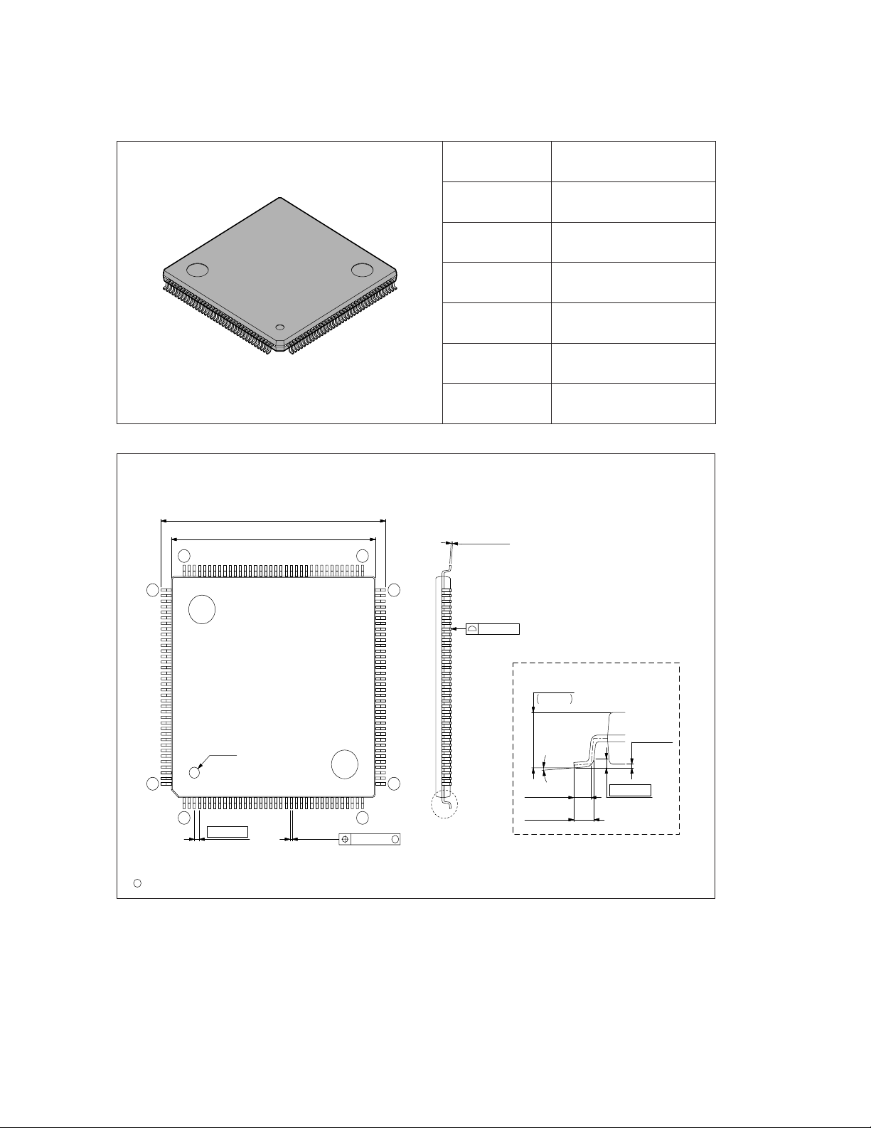
1.3 Package Dimensions
Two types of MB91150 packages are provided.
■ Package dimensions of PGA-299C-A01 (MB91FV150 Only)
Figure 1.3-1 Package dimensions of PGA-299C-A01
299-pin ceramic PGA Lead pitch 2.54mm(100mil)
Sealing method Metal seal
CHAPTER 1 OVERVIEW OF THE MB91150
Pin matrix 20
(PGA-299C-A01)
299-pin ceramic PGA
(PGA-299C-A01)
INDEX AREA
2.41 ± 0.10
(.095 ± .004)
1.65 ± 0.10
(.065 ± .004)
30.48 ± 0.31
(1.200 ± .012)
52.32 ± 0.56
(2.060 ± .022)
SQ
35.56 ± 0.41
(1.400 ± .016)
3.94 ± 0.10
(.155 ± .004)
5.59 (.220) MAX
+ 0.13
0.46
+ .005
(.018 )
2.54 (.100) MAX
48.26 (19.00)
REF
2.54 ± 0.25
(.100 ± .010)
1.27 ± 0.25
(.050 ± .010)
+ 0.41
3.40
+ .016
(.134 )
1.27 (.050) DIA TYP
(4 PLCS)
INDEX AREA
C
1994 FUJITSU LIMITED R299001SC-2-2
Dimensions in mm (inches).
7
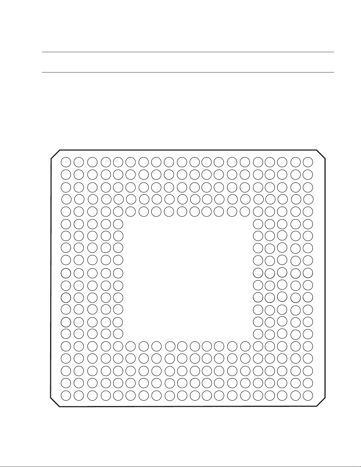
Page 24
CHAPTER 1 OVERVIEW OF THE MB91150
■ Package dimensions of FPT-144P-M08 (MB91F155A, MB91155 and MB91154)
Figure 1.3-2 Package dimensions of FPT-144P-M08
144-pin plastic LQFP Lead pitch 0.50 mm
(FPT-144P-M08)
144-pin plastic LQFP
(FPT-144P-M08)
22.00±0.20(.866±.008)SQ
*
20.00±0.10(.787±.004)SQ
109
Package width ×
package length
20.0 × 20.0 mm
Lead shape Gullwing
Sealing method Plastic mold
Mounting height
1.70 mm MAX
Weight 1.20g
Code
(Reference)
Note 1)*:Values do not include resin protrusion.
Resin protrusion is +0.25(.010)Max(each side).
Note 2) Pins width and pins thickness include plating thickness.
Note 3) Pins width do not include tie bar cutting remainder.
0.145±0.055
73108
72
(.006±.002)
P-LFQFP144-20×20-0.50
INDEX
144
1 36
LEAD No.
C
2003 FUJITSU LIMITED F144019S-c-4-6
0.50(.020)
0.22±0.05
(.009±.002)
0.08(.003)
0.08(.003)
Details of "A" part
+0.20
1.50
–0.10
(Mounting height)
+.008
.059
–.004
0.10±0.10
0˚~8˚
37
M
"A"
0.50±0.20
(.020±.008)
0.60±0.15
(.024±.006)
Dimensions in mm (inches).
Note: The values in parentheses are reference values.
(.004±.004)
(Stand off)
0.25(.010)
8
Page 25
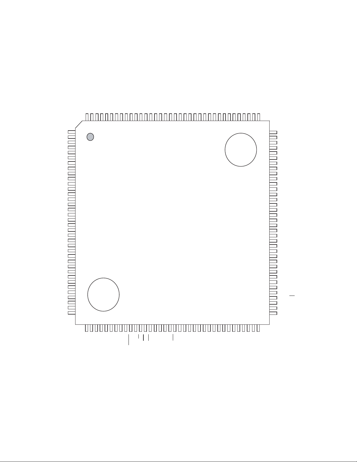
CHAPTER 1 OVERVIEW OF THE MB91150
1.4 Pin Assignment
This section shows the MB91150 pin assignment for each type of package.
■ Pin assignment of MB91FV150 (PGA-299C-A01)
Figure 1.4-1 "MB91FV150 (PGA-299C-A01) pin assignment" shows the MB91FV150 (PGA299C-A01) pin assignment. Table 1.4-1 "Correspondence between pin numbers and pin names
(MB91FV150 (PGA-299C-A01)) (Device: MB91FV150, Package: PGA-299C-A01)" lists the
correspondences between pin numbers and pin names.
Figure 1.4-1 MB91FV150 (PGA-299C-A01) pin assignment
3
2
5
8
25
27
32
34
22
29
37
50
53
296299
292
298
4
10
13
6
16 11
15 12
19
18
23
24
26
33
3839
40 41 4243
444546 47 48
51
54 565758
55
60 61
270
274 275
277 278
293
280
283
286
289
284
287
291
297
285
290
295
300
288
294
1
7
9
14
17
2021
28
3031
35 36
64
264
265
267
266
262
263
261
259
260
268
276
279
281
282
269
271
272
273
PGA-299C-A01
(Bottom View)
254
258
256
255
253
247
251
249
246
244
257
248
242
241
238
252
243
239
236
232
245
250
240
237
235
226231
222
227
220
216
214
208
206
198
197
193
186
185
178
180
170 171
164
167
233
234
228229
223
217
213
210211
204
196
191192
188
181
174
168
230
225
215
212
209
205
201
194
190
189
183
176
173
224
221
218219
207
202
199
195
203
200
187
179
172
184
182
59
49
52
62
65
68 69
71
75
80
74
66
63
67
72
73
76
78 79
84
87
83
95
70
82
77
86
81
85
89
90
93
100 102
88
91
92
98
107
94
96
99
101
97
103
105
106
108
104
110
116
117
109
111
115
113
114
112
125 118
123
122
121
119
133
131
129
126
139
136
135
130
120
145
141
138
134
124
159
153
147
142
137
127128
165
162
157
161
156
151
148
154 155
140
144
132
143
169
166
163
160
150
146
177
175
158
152
149
9
Page 26

CHAPTER 1 OVERVIEW OF THE MB91150
Table 1.4-1 Correspondence between pin numbers and pin names (MB91FV150 (PGA-299C-A01))
(Device: MB91FV150, Package: PGA-299C-A01)
No. Pin name No. Pin name No. Pin name No. Pin name No. Pin name No. Pin name
1 P20/D16 51 P81/BGRNT
2V
SS
3OPEN 53V
52 P82/BRQ 102 PK2/AN2 152 V
CC
4 P21/D17 54 P83/RD
5V
CC
55 P84/WR0 105 PK4/AN4 155 V
6 P22/D18 56 P85/WR1
7 P23/D19 57 P86/CLK 107 PK6/AN6 157 PE0/OC0 207 IHIT0 257 TDT33
8V
SS
58 PL0/DREQ0 108 PK7/AN7 158 V
9 P24/D20 59 PL1/DACK0 109 DAVC 159 PE1/OC1 209 OPEN 259 OPEN
10 P25/D21 60 PL2/DEOP0 110 DAVS 160 PE2/OC2 210 OPEN 260 OPEN
11 P26/D22 61 PL3/DREQ1 111 DA0 161 PE3/OC3 211 V
12 P27/D23 62 PL4/DACK1 112 V
13 P30/D24 63 PL5/DEOP1 113 DA1 163 PE5/OC5 213 MOD30 263 TDT38
14 P31/D25 64 PL6/DREQ2 114 DA2 164 PE6/OC6 214 MOD29 264 TDT39
15 P32/D26 65 PL7/DACK2 115 PH0/SIN0 165 PE7/OC7 215 MOD28 265 TDT40
16 P33/D27 66 OPEN 116 PH1/SOT0 166 V
17 P34/D28 67 OPEN 117 PH2/SCK0/T00 167 PF0/IN0 217 MOD26 267 TDT42
18 P35/D29 68 V
CC
19 P36/D30 69 OPEN 119 PI1/SOT1 169 PF2/IN2 219 MOD25 269 V
20 P37/D31 70 OPEN 120 PI2/SCK1/T01 170 PF3/IN3 220 MOD24 270 OPEN
21 P40/A00 71 V
22 V
CC
72 OPEN 122 PI4/SOT2 172 V
SS
23 P41/A01 73 OPEN 123 PI5/SCK2/T02 173 PG0/PPG0 223 MOD22 273 OPEN
24 P42/A02 74 V
CC
25 P43/A03 75 OPEN 125 V
26 P44/A04 76 MD0 126 PI4/SOT3 176 PG3/PPG3 226 MOD20 276 TDT49
27 P45/A05 77 MD1 127 PI5/SCK3/T03 177 PG4/PPG4 227 MOD19 277 TDT50
28 P46/A06 78 MD2 128 V
29 V
SS
30 P47/A07 80 V
79 V
CC
SS
31 P50/A08 81 X0 131 OPEN 181 OPEN 231 MOD16 281 OPEN
32 P51/A09 82 X1 132 OPEN 182 OPEN 232 MOD15 282 OPEN
33 P52/A10 83 V
CC
34 P53/A11 84 RST
35 P54/A12 85 OPEN 135 V
36 P55/A13 86 ICLK 136 PC0/INT0 186 OPEN 236 MOD12 286 V
37 V
CC
87 ICS0 137 PC1/INT1 187 V
38 P56/A14 88 ICS1 138 PC2/INT2 188 OPEN 238 MOD10 288 OPEN
39 P57/A15 89 ICS2 139 PC3/INT3 189 OPEN 239 MOD9 289 OPEN
40 P60/A16 90 ICD0 140 PC4/INT4/CS0 190 OPEN 240 V
41 P61/A17 91 ICD1 141 PC5/INT5/CS1 191 MCLK 241 MOD8 291 OPEN
42 P62/A18 92 ICD2 142 PC6/INT6/CS2 192 MRST
43 P63/A19 93 ICD3 143 V
44 P64/A20 94 BREAK 144 PC7/INT7/CS3 194 DHIT5 244 MOD5 294 OPEN
45 P65/A21 95 AV
CC
46 P66/A22 96 AVRH 146 V
47 P67/A23 97 V
SS
48 P80/RDY 98 AVRL 148 PD2/INT10/AIN1 198 DHIT1 248 MOD2 298 OPEN
49 V
50 V
CC
SS
99 AV
SS
100 PK0/AN0 150 PD3/INT11/BIN1 200 V
101 PK1/AN1 151 PD4/INT12/ZIN0 201 OPEN 251 OPEN
103 PK3/AN3 153 PD5/INT13/ZIN1 203 V
SS
202 OPEN 252 OPEN
CC
253 OPEN
104 OPEN 154 PD6/INT14/DEOP2 204 IHIT3 254 VCC5
CC
205 IHIT2 255 TDT31
106 PK5/AN5 156 PD7/INT15/ATG 206 IHIT1 256 TDT32
SS
SS
162 PE4/OC4 212 MOD31 262 V
CC
118 PI0/SIN1 168 PF1/IN1 218 V
121 PI3/SIN2 171 PF4 221 V
CC
124 PJ0/SIN3 174 PG1/PPG1 224 V
CC
SS
129 OPEN 179 V
175 PG2/PPG2 225 MOD21 275 VCC5
178 PG5/PPG5 228 MOD18 278 V
SS
130 OPEN 180 OPEN 230 V
133 PJ0/SCL 183 OPEN 233 V
208 OPEN 258 TDT34
CC
261 OPEN
SS
216 MOD27 266 TDT41
SS
CC
268 OPEN
3
CC
271 OPEN
222 MOD23 272 OPEN
SS
274 OPEN
SS
229 MOD17 279 OPEN
CC
SS
280 OPEN
283 OPEN
134 PJ1/SDA 184 OPEN 234 MOD14 284 OPEN
SS
185 OPEN 235 MOD13 285 OPEN
CC
CC
237 MOD11 287 OPEN
CC
290 OPEN
242 MOD7 292 OPEN
CC
193 V
CC
243 MOD6 293 V
CC
145 PD0/INT8/AIN0 195 DHIT4 245 MOD4 295 OPEN
SS
147 PD1/INT9/BIN0 197 DHIT2 247 V
149 V
CC
196 DHIT3 246 MOD3 296 V
SS
297 OPEN
199 DHIT0 249 MOD1 299 V
SS
250 MOD0 300 OPEN
SS
CC
10
Page 27
CHAPTER 1 OVERVIEW OF THE MB91150
6
5
5PD6/DEOP2/
5/
G5
■ Pin assignments of MB91F155A, MB91155, MB91154 (FPT-144P-M08) and MB91F155A (FPT-144P-M01)
Figure 1.4-2 "Pin assignments of MB91F155A, MB91155, MB91154 (FPT-144P-M08) and
MB91F155A (FPT-144P-M01)" shows the MB91F155A, MB91155, MB91154 (FPT-144P-M08)
and MB91F155A (FPT-144P-M01) pin assignments.
Figure 1.4-2 Pin assignments of MB91F155A, MB91155, MB91154 (FPT-144P-M08) and
MB91F155A (FPT-144P-M01)
VSSX1A
X0A
TEST
VCCPK7/AN7
PK6/AN6
PK5/AN5
PK4/AN4
PK3/AN3
PK2/AN2
PK1/AN1
PK0/AN0
AVSSAVRL
AVRH
AVCCDAVC
DAVS
DA0
DA1
DA2
VCCPL7/DACK2
PL6/DREQ2
PL5/DEOP1
PL4/DACK1
PL3/DREQ1
PL2/DEOP0
PL1/DACK0
PL0/DREQ0
PH0/SIN0
PH1/SOT0
PH2/SCK0/TO0
PH3/SIN1
PH4/SOT1
144
143
142
141
140
139
138
137
136
135
134
133
132
131
130
129
128
127
126
125
124
123
122
121
120
119
118
117
116
115
114
113
112
111
110
P20/D16 1 108
P21/D17 2 107
P22/D18 3 106
P23/D19 4 105
P24/D20 5 104
P25/D21 6 103
P26/D22 7 102
P27/D23 8 101
V
P30/D24 10 99
P31/D25 11 98
P32/D26 12 97
P33/D27 13 96
P34/D28 14 95
P35/D29 15 94
P36/D30 16 93
P37/D31 17 92
P40/A00 18 91
P41/A01 19 90
P42/A02 20 89
P43/A03 21 88 PF2/IN2
P44/A04 22 87 PF1/IN1
P45/A05 23 86 PF0/IN0
P46/A06 24 85 PE7/OC7
P47/A07 25 84 PE6/OC6
V
V
P50/A08 28 81 PE3/OC3
P51/A09 29 80 PE2/OC2
P52/A10 30 79 PE1/OC1
P53/A11 31 78 PE0/OC0
P54/A12 32 77 V
P55/A13 33 7
P56/A14 34 7
P57/A15 35 74 P D
P60/A16 36 7
9 100
SS
Top View
FPT-144P-M08
26 83 PE5/OC5
SS
27 82 PE4/OC4
CC
3738394041424344454647484950515253545556575859606162636465666768697071
FPT-144P-M01
109
72
PH5/SCK1/TO1
PI0/SIN2
PI1/SOT2
PI2/SCK2/TO2
PI3/SIN3
PI4/SOT3
PI5/SCK3/TO3
V
SS
PJ0/SCL
PJ1/SDA
V
SS
V
CC
PG5/PPG5
PG4/PPG4
PG3/PPG3
PG2/PPG2
PG1/PPG1
PG0/PPG0
PF4
PF3/IN3
CC
PD7/ATG/INT1
ZIN1/INT13/TR
PD4
ZIN
INT12TR4
INT14
P61/A17
P62/A18
P63/A19
P64/A20
P65/A21
P66/A22
SS
V
P67/A23
P80/RDY
P81/BGRNT
P83/RD
P82/BRQ
P84/WR0
P86/CLK
P85/WR1
MD2
MD1
MD0
RST
SS
CC
X1
X0
V
V
PC0/INT0
PC1/INT1
PC2/INT2
PC3/INT3
PC4/INT4/CS0
CC
V
PC5/INT5/CS1
PC6/INT6/CS2
PC7/INT7/CS3
PD0/AIN0/INT8/TRG0
PD1/BIN0/INT9/TRG1
PD2/AIN1/INT10/TRG2
PD3/BIN1/INT11/TRG3
11
Page 28

CHAPTER 1 OVERVIEW OF THE MB91150
1.5 Pin Functions
Table 1.5-1 "Functions of the MB91150 pins" lists the functions of the MB91150 pins.
■ Functions of the MB91150 pins
Table 1.5-1 Functions of the MB91150 pins
Pin No. Pin name Circuit type Function description
1
2
3
4
5
6
7
8
10
11
12
13
14
15
16
17
18
19
20
21
22
23
24
25
28
29
30
31
32
33
34
35
P20/D16
P21/D17
P22/D18
P23/D19
P24/D20
P25/D21
P26/D22
P27/D23
P30/D24
P31/D25
P32/D26
P33/D27
P34/D28
P35/D29
P36/D30
P37/D31
P40/A00
P41/A01
P42/A02
P43/A03
P44/A04
P45/A05
P46/A06
P47/A07
P50/A08
P51/A09
P52/A10
P53/A11
P54/A12
P55/A13
P56/A14
P57/A15
C External data bus bits 16 to 23
Effective only in external bus 16-bit mode.
Can be used as a port in single chip or external bus 8bit mode.
C External data bus bits 24 to 31
Can be used as a port in single chip mode.
F External address bus bits 0 to 15
Effective in external bus mode.
Can be used as a port in single chip mode.
12
Page 29

CHAPTER 1 OVERVIEW OF THE MB91150
Table 1.5-1 Functions of the MB91150 pins (Continued)
Pin No. Pin name Circuit type Function description
36
37
38
39
40
41
42
43
P60/A16
P61/A17
P62/A18
P63/A19
P64/A20
P65/A21
P66/A22
P67/A23
O External address bus bits 16 to 23
Can be used as a port when the address bus is not
used.
45 P80/RDY C External RDY input
Effective when external RDYU input is enabled.
"0" is input if the bus cycle in progress fails to be
complete.
Can be used as a port when external RDY input is not
used.
46 P81/BGRNT
F External bus open acceptance output
Effective when external bus open acceptance output is
enabled.
Outputs L when the external bus is opened.
Can be used as a port when external bus open
acceptance output is disabled.
47 P82/BRQ C External bus open request input
Effective when external bus open request input is
enabled.
Input "1" to open the external bus.
Can be used as a port when external bus open
request input is disabled.
48 P83/RD
F External bus read strobe output
Effective when external bus read strobe output is
enabled.
Can be used as a port when external bus read strobe
output is disabled.
49 P84/WR0
F External bus write strobe output
Effective in external bus mode.
Can be used as a port in single chip mode.
50 P85/WR1
F External bus write strobe output
Effective when MB91150 is in external bus mode and
bus width is 16 bits.
Can be used as a port when MB91150 is in single chip
mode or 8-bit external bus mode.
51 P86/CLK F System clock output
Outputs a clock signal that is equal to the operating
frequency of the external bus. Can be used as a port
when the system clock is not used.
52
53
54
55 RST
MD2
MD1
MD0
G Connect these pins directly to V
These pins set the basic MCU operation mode.
Mode pins
B External reset input
or VSS.
CC
13
Page 30

CHAPTER 1 OVERVIEW OF THE MB91150
Table 1.5-1 Functions of the MB91150 pins (Continued)
Pin No. Pin name Circuit type Function description
57
58
60
61
62
63
64
65
66
67
X1
X0
PC0/INT0
PC1/INT1
PC2/INT2
PC3/INT3
PC4/INT4/CS0
PC5/INT5/CS1
PC6/INT6/CS2
PC7/INT7/CS3
A High-speed clock oscillation pins (16.5 MHz)
H External interrupt request inputs 0 to 3
These inputs are always in use while the
corresponding external interrupts are enabled. Stop
port output in advance unless the resulting processing
is intentional.
This port can be used to release the standby status
because its input is enabled even during standby.
Can be used as a port when the pin is not used for
external interrupt request input.
H Used for both chip select outputs and external interrupt
request inputs 4 to 7
Can be used for external interrupt request input or as a
port when chip select output is disabled.
These inputs are always in use while the
corresponding external interrupts are enabled. Stop
port output in advance unless the resulting processing
is intentional.
This port can be used to release the standby status
because its input is enabled even during standby.
Can be used as a port when the pin is not used for
external interrupt request input and chip select output.
69
70
71
72
73
74
75 PD6/DEOP2/INT14 H External interrupt request input 14
PD0/AIN0/INT8/TRG0
PD1/BIN0/INT9/TRG1
PD2/AIN1/INT10/TRG2
PD3/BIN1/INT11/TRG3
PD4/ZIN0/INT12/TRG4
PD5/ZIN1/INT13/TRG5
H External interrupt request inputs 8 to 13
These inputs are always in use while the
corresponding external interrupts are enabled. Stop
port output in advance unless the resulting processing
is intentional.
[AIN, BIN] Up/down timer input
[TRG] PPG external trigger input
These inputs are always in use while they are enabled.
Stop port output in advance unless the resulting
processing is intentional.
Can be used as a timer when the pin is not used for
external interrupt request input, up/down timer input,
and PPG external trigger input.
This input is always in use while the corresponding
external interrupt is enabled. Stop port output in
advance unless the resulting processing is intentional.
[DEOP2] DMA external transfer end output
Effective when DMAC external transfer end output
specification is enabled.
Can be used as a port when the pin is not used for
external interrupt request input or DMA external
transfer end output.
14
Page 31

CHAPTER 1 OVERVIEW OF THE MB91150
Table 1.5-1 Functions of the MB91150 pins (Continued)
Pin No. Pin name Circuit type Function description
76 PD7/ATG
78
79
80
81
82
83
84
85
86
87
88
89
PE0/OC0
PE1/OC1
PE2/OC2
PE3/OC3
PE4/OC4
PE5/OC5
PE6/OC6
PE7/OC7
PF0/IN0
PF1/IN1
PF2/IN2
PF3/IN3
/INT15 H External interrupt request input 15
This input is always in use while the corresponding
external interrupt is enabled. Stop port output in
advance unless the resulting processing is intentional.
[ATG
] A/D converter external trigger input
This input is always in use while the corresponding
external interrupt is enabled. Stop port output in
advance unless the resulting processing is intentional.
Can be used as a port when the pin is not used for
external interrupt request input and A/D converter
external trigger input.
F Output compare output
Can be used as a port when output compare output
specification is disabled.
F Input capture input
Effective for input with input capture.
Can be used as a port when the pin is not used as
Input capture input.
90 PF4 F General-purpose I/O port
91
92
93
94
95
96
PG0/PPG0
PG1/PPG1
PG2/PPG2
PG3/PPG3
PG4/PPG4
PG5/PPG5
99 PJ1/SDA Q I
F PPG timer output
Effective when PPG timer output specification is
enabled.
Can be used as a port when PPG timer output
specification is disabled.
2
C interface data I/O pin
Effective when I
Set port output to Hi-Z while the I
2
C interface operation is enabled.
2
C interface is
operating.
2
C is not used.
2
C interface is
100 PJ0/SCL Q I
Can be used as a port when I
2
C interface I/O pin
Effective when I
2
C interface operation is enabled.
Set port output to Hi-Z while the I
operating.
Can be used as a port when I
2
C is not used.
102 PI5/SCK3/TO3 P UART3 clock I/O, Reload Timer 3 output
Acts as output for Reload Timer 3 when UART3 clock
output is disabled and Reload Timer 3 output is
enabled.
Can be used as port when UART3 clock output and
reload timer output are disabled.
15
Page 32

CHAPTER 1 OVERVIEW OF THE MB91150
Table 1.5-1 Functions of the MB91150 pins (Continued)
Pin No. Pin name Circuit type Function description
103 PI4/SOT3 P UART3 data output
Effective when UART3 data output specification is
enabled.
Can be used as a port when UART3 data output
specification is disabled.
104 PI3/SIN3 P UART3 data input
This input is always in use while UART3 is performing
input processing. Stop port output in advance unless
the resulting processing is intentional.
Can be used as a port when the pin is not used for
UART3 data input.
105 PI2/SCK2/TO2 P UART2 clock I/O, Reload Timer 2 output
Acts as output for Reload Timer 2 when UART2 clock
output is disabled and Reload Timer 2 output is
enabled.
Can be used as port when UART2 clock output and
reload timer output are disabled.
106 PI1/SOT2 P UART2 data output
Effective when UART2 data output specification is
enabled.
Can be used as a port when UART2 data output
specification is disabled.
107 PI0/SIN2 P UART2 data input
This input is always in use while UART2 is performing
input processing. Stop port output in advance unless
the resulting processing is intentional.
Can be used as a port when the pin is not used for
UART2 data input.
108 PH5/SCK1/TO1 P UART1 clock I/O, Reload Timer 1 output
Acts as output for Reload Timer 1 when UART1 clock
output is disabled and Reload Timer 1 output is
enabled.
Can be used as port when UART1 clock output and
reload timer output are disabled.
109 PH4/SOT1 P UART1 data output
Effective when UART1 data output specification is
enabled.
Can be used as a port when UART1 data output
specification is disabled.
110 PH3/SIN1 P UART1 data input
This input is always in use while UART1 is performing
input processing. Stop port output in advance unless
the resulting processing is intentional.
Can be used as a port when the pin is not used for
UART1 data input.
16
Page 33

CHAPTER 1 OVERVIEW OF THE MB91150
Table 1.5-1 Functions of the MB91150 pins (Continued)
Pin No. Pin name Circuit type Function description
111 PH2/SCK0/TO0 P UART0 clock I/O, Reload Timer 0 output
Acts as output for Reload Timer 0 when UART0 clock
output is disabled and Reload Timer 0 output is
enabled.
Can be used as port when UART0 clock output and
reload timer output are disabled.
112 PH1/SOT0 P UART0 data output
Effective when UART0 data output specification is
enabled.
Can be used as a port when UART0 data output
specification is disabled.
113 PH0/SIN0 P UART0 data input
This input is always in use while UART0 is performing
input processing. Stop port output in advance unless
the resulting processing is intentional.
Can be used as a port when the pin is not used for
UART0 data input.
114 PL0/DREQ0 F DMA external transfer request input
This pin is always in use when the pin is selected for a
DMA controller transfer source. Stop port output in
advance unless the resulting processing is intentional.
Can be used as a port when the pin is not used for
DMA transfer request input.
115 PL1/DACK0 F DMA external transfer request acceptance output
Effective when external transfer request acceptance
output specification of the DMA controller is enabled.
Can be used as a port when external transfer request
acceptance output specification of the DMA controller
is disabled.
116 PL2/DEOP0 F DMA external transfer end output
Effective when external transfer end output
specification of the DMA controller is enabled.
117 PL3/DREQ1 F DMA external transfer request input
This pin is always in use when the pin is selected for a
DMA controller transfer source. Stop port output in
advance unless the resulting processing is intentional.
Can be used as a port when the pin is not used for
DMA transfer request input.
118 PL4/DACK1 F DMA external transfer request acceptance output
Effective when external transfer request acceptance
output specification of the DMA controller is enabled.
Can be used as a port when external transfer request
acceptance output specification of the DMA controller
is disabled.
119 PL5/DEOP1 F DMA external transfer end output
Effective when external transfer end output
specification of the DMA controller is enabled.
17
Page 34

CHAPTER 1 OVERVIEW OF THE MB91150
Table 1.5-1 Functions of the MB91150 pins (Continued)
Pin No. Pin name Circuit type Function description
120 PL6/DREQ2 F DMA external transfer request input
This pin is always in use when the pin is selected for a
DMA controller transfer source. Stop port output in
advance unless the resulting processing is intentional.
Can be used as a port when the pin is not used as
DMA transfer request input.
121 PL7/DACK2 F DMA external transfer request acceptance output
Effective when external transfer request acceptance
output specification of the DMA controller is enabled.
Can be used as a port when external transfer request
acceptance output specification of the DMA controller
is disabled.
123
124
125
DA2
DA1
DA0
- D/A converter output
Effective when D/A converter output specification is
enabled.
126 DAVS - Power supply pin of D/A converter
127 DAVC - Power supply pin of D/A converter
128 AV
CC
-V
power supply for A/D converter
CC
129 AVRH - A/D converter reference voltage (high potential side)
Be sure to turn on or off this pin when a potential of
AVRH or higher is applied to V
CC
.
130 AVRL - A/D converter reference voltage (low potential side)
131 AV
132
133
134
135
136
137
138
139
PK0/AN0
PK1/AN1
PK2/AN2
PK3/AN3
PK4/AN4
PK5/AN5
PK6/AN6
PK7/AN7
SS
-V
N A/D converter analog input
power supply for A/D converter
SS
Effective when the AIC register specifies analog input.
Can be used as a port when A/D converter analog
input is not used.
141 TEST G Always connect the pin to the V
142
143
27, 56,
68, 77,
X0A
X1A
V
CC
K Oscillation pins for low-speed clock frequency (32 kHz)
- Power supply of digital circuit
Be sure to connect the power supply to all V
97, 122,
140
18
power supply.
CC
CC
pins.
Page 35

CHAPTER 1 OVERVIEW OF THE MB91150
Table 1.5-1 Functions of the MB91150 pins (Continued)
Pin No. Pin name Circuit type Function description
9,26,
44, 59,
V
SS
- Ground level of digital circuit
Be sure to ground the power supply to all V
98, 101,
144
Note:
For most of the above pins, port I/O and resource I/O are multiplexed as in xxx/Pxx.
If port and resource outputs compete at these pins, resource output precedes port output.
SS
pins.
19
Page 36

CHAPTER 1 OVERVIEW OF THE MB91150
1.6 I/O Circuit Types
Table 1.6-1 "I/O circuit types" shows the MB91150 I/O circuit types.
■ I/O circuit types
Table 1.6-1 I/O circuit types
Classification Circuit Remarks
• High-speed oscillator (16.5
MHz)
X1
Xout
Oscillation feedback resistor:
about 1 MΩ
A
X0
Standby control signal
• CMOS hysteresis input pin
CMOS hysteresis input
(Without standby control)
With pull-up resistance
B
Digital input
• CMOS level I/O pin
CMOS level output
CMOS level input
Pout
(With standby control)
IOL=4mA
C
Nout
20
R
CMOS input
Standby control
Page 37

CHAPTER 1 OVERVIEW OF THE MB91150
X
Table 1.6-1 I/O circuit types
Classification Circuit Remarks
• CMOS hysteresis I/O pin
CMOS level output
CMOS hysteresis input
Pout
(With standby control)
IOL=4mA
F
R
Nout
Hysteresis input
Standby control
• CMOS level input pin
CMOS level input
(Without standby control)
G
R
Digital input
• CMOS hysteresis I/O pin with
Pull-up control
pull-up control
CMOS level output
CMOS hysteresis input
R
Pout
H
(Without standby control)
Pull-up resistance: about 50 KΩ
(typically)
Nout
IOL=4mA
R
Hysteresis input
• Clock oscillation circuit (32 kHz)
X1A
K
0A
Xout
21
Page 38

CHAPTER 1 OVERVIEW OF THE MB91150
Nout
R
R
Table 1.6-1 I/O circuit types
Classification Circuit Remarks
Pout
• Analog/CMOS level I/O pin
CMOS level output
CMOS level input
N
R
Nout
(With standby control)
Analog input
(Analog input is enabled when
CMOS input
Standby control
Analog input
the bit corresponding AIC is 1.)
IOL=4mA
• CMOS hysteresis I/O pin with
pull-up control
Pull-up control
CMOS level output
CMOS hysteresis input
R
Pout
(With standby control)
Pull-up resistance: about 50 KΩ
O
Nout
R
Hysteresis input
Standby control
(typically)
IOL=4mA
• CMOS hysteresis I/O pin with
Pull-up control
Open-drain control
pull-up control
CMOS level output
(With open-drain control)
CMOS hysteresis input
(With standby control)
P
Pull-up resistance: about 50 KΩ
(typically)
IOL=4mA
Hysteresis input
Standby control
• Open-drain I/O pin
• 5 V dielectric strength
• CMOS hysteresis input
Nout
Q
(With standby control)
IOL=15mA
R
Hysteresis input
Standby control
22
Page 39

CHAPTER 2 HANDLING THE DEVICE
This chapter provides details on handling the MB91150.
2.1 "Notes on Handling the MB91130"
2.2 "Notes on Using Devices"
2.3 "Power-On"
23
Page 40

CHAPTER 2 HANDLING THE DEVICE
2.1 Notes on Handling Devices
This section describes latch-up prevention, pin processing, and circuit handling.
■ Latch-up prevention
CMOS ICs may suffer a latch-up when a higher voltage than V
applied to an input or output pin or when a voltage exceeding the applicable rating is applied
between V
thermal damage to an element. For this reason, ensure that the voltage to be applied does not
exceed the absolute maximum ratings.
■ Pin processing
❍ Unused pin processing
Leaving unused input pins open may result in a malfunction; pull them up or down.
❍ NC pin processing
Be sure to open the NC pin when using it.
❍ Output pin processing
Connecting one output pin with another, connecting an output pin with the power supply, or
connecting a large capacity load may cause flow of high current. Over a long period, this
condition results in device deterioration. For this reason, ensure that the current does not
exceed the absolute maximum ratings.
❍ Mode pins (MD0 to MD2)
or a lower voltage than VSS is
CC
and VSS. This latch-up may rapidly increase power supply current, resulting in
CC
24
Connect the MD0 to MD2 pins direct to V
or VSS when using them. To prevent MB91150 from
CC
entering the test mode mistakenly due to noise, make the pattern length between each mode
pin and V
or VSS on a PC board as short as possible and connect these in low impedance.
CC
❍ Power supply pins
If there are several V
and VSS pins, those that must be set to the same potential in the device
CC
are connected to each other in device design to prevent such malfunctions as latch-up. To
prevent the strobe signal from malfunctioning due to fluctuations in background radiation and
increase in ground level current or to observe the total output current regulations, be sure to
externally connect all these power supply pins to the power supply and ground.
Also, connect the power supply pins from the power supply source to the V
and VSS pins of
CC
this device at low impedance as far as possible. In addition, a ceramic capacitor of about 0.1µF
should be connected between V
and VSS pins near this device as a bypass capacitor.
CC
Page 41

■ Circuit handling
❍ Crystal oscillation circuit
Noise near the X0, X1, X0A, or X1A pin causes this device to malfunction. Design PC boards so
that the X0 and X1 (X0A and X1A) pins, crystal oscillators (or ceramic oscillators), and bypass
capacitors to the ground can be placed as close as possible.
In the interest of stable operation, it is strongly recommended that a PC board artwork that
encloses the surroundings of the X0, X1, X0A, and X1A pins with the ground should be used.
The MB91FV150 has a feedback resistor in the 32 kHz oscillation circuit (X0A, X1A), but the
MB91F155A, MB91155 and MB91154 do not. Therefore, when the clock function is used,
connect an external resistor as shown in Figure 2.1-1 "Resistor connection".
Figure 2.1-1 Resistor connection
X0A
CHAPTER 2 HANDLING THE DEVICE
X0A
X1A
MB91FV150
MB91F155A
X1A
MB91155/MB91154
25
Page 42

CHAPTER 2 HANDLING THE DEVICE
2.2 Notes on Using Devices
This section provides notes on using external reset input and external clocks.
■ External reset input
To securely put the device into the reset state, at least five machine cycles of L level input to the
RST
pin are required.
■ External clock
When an external clock is used, feed the clock to the X0 pin and antiphase clock to the X1 pin
simultaneously. However, when the STOP mode (oscillation stop mode) is also used, the X1 pin
stops with H output in STOP mode. To prevent output collision, provide an external resistor of
about 1 kΩ.
Figure 2.2-1 "Example of using an external clock" shows an example of using an external clock.
Figure 2.2-1 Example of using an external clock
X0
■ Notes on during operation of PLL clock mode
If the PLL clock mode is selected, the microcontroller attempt to be working with the selfoscillating circuit even when there is no external oscillator or external clock input is stopped.
Performance of this operation, however, cannot be guaranteed.
■ Watchdog timer function
The watchdog timer supported by the FR family monitors the program that performs the reset
delay operation for a specified time. If the program hangs and the reset delay operation is not
performed, the watchdog timer resets the CPU. Therefore, once the watchdog timer is enabled,
operation continues until the CPU is reset.
As an exception, a reset delay automatically occurs if the CPU stops program execution. For the
conditions that apply to this exception, refer to the section that describes the watchdog function.
X1
MB91150
26
Page 43

CHAPTER 2 HANDLING THE DEVICE
2.3 Power-On
This section provides notes on power-on and notes applicable when the clock function
is not used.
■ Notes on power-on
❍ Power-on
At power-on, be sure to start the RST
the V
elapsed, then set the RST
level, wait until the time for at least five cycles of the internal operating clock has
CC
pin to the H level.
pin at the L level. After the power supply level becomes
❍ Oscillation input
At power-on, be sure to continue inputting clock signals until the oscillation stabilization wait
status is released.
❍ Power-on reset
Be sure to perform a power-on reset to turn on power. Perform a power-on reset also when
powering on again if the power supply voltage has dropped to less than the voltage for assuring
operation.
❍ Power on order
Turn on power in the order of V
--> AVCC --> AVRH, and turn off power in the reverse order.
CC
❍ A/D converter
Even when the A/D converter is not used, connect AV
to the VCC level and AVSS to the V
CC
level.
❍ D/A converter
Even when the D/A converter is not used, connect DAVC to the V
level and DAVS to the V
CC
level.
SS
SS
27
Page 44

CHAPTER 2 HANDLING THE DEVICE
■ When the clock function (calendar macro) Is not used
When the clock function is not used, arrange the clock oscillation pins as shown in Figure 2.3-1
"Arrangement of clock oscillation pins when the clock function is not used".
Figure 2.3-1 Arrangement of clock oscillation pins when the clock function is not used
X0A
OPEN
X1A
MB91150
Note:
The crystal oscillator for the clock used in this type of product cannot be stopped by
software.
28
Page 45

CHAPTER 3 MEMORY SPACE, CPU AND CONTROL
UNIT
This chapter provides basic information regarding the architecture, specifications,
instructions, and other topics, that is required to understand the CPU core functions of
the FR series.
3.1 "Memory Space"
3.2 "CPU Architecture"
3.3 "Programming Model"
3.4 "Data Structure"
3.5 "Word Alignment"
3.6 "Special Memory Areas"
3.7 "Overview of Instructions"
3.8 "EIT (Exception, Interrupt, and Trap)"
3.9 "Reset Sequence"
3.10 "Operation Mode"
3.11 "Clock Generator (Low-Power Consumption Mechanism)"
3.12 "Low-Power Consumption Mode"
29
Page 46

CHAPTER 3 MEMORY SPACE, CPU AND CONTROL UNIT
3.1 Memory Space
The logical address space of the FR series is four gigabytes (232 addresses). The CPU
accesses this space linearly.
■ Direct addressing area
The following area of the address space is used for I/O operations.
This area is called the direct addressing area. The addresses in this area can directly be
specified in instruction operands.
The size of the direct area varies depending on the size of data to be accessed as follows:
• Byte data access: 000
• Half word data access: 000H to 1FFH
• Word data access: 000
to 0FFH
H
to 3FF
H
H
30
Page 47

CHAPTER 3 MEMORY SPACE, CPU AND CONTROL UNIT
■ Memory map for MB91FV150, MB91F155A and MB91155
Figure 3.1-1 "Memory map for MB91FV150, MB91F155A and MB91155" shows the memory
space allocation for the MB91FV150, MB91F155A and MB91155.
Figure 3.1-1 Memory map for MB91FV150, MB91F155A and MB91155
0000 0000
0000 0400
0000 0800
0000 1000
0000 9000
0001 0000
FFFF FFFF
External ROM
external bus mode
H
I/O I/O I/O
H
I/O I/O I/O
H
Access disabled
H
Built-in RAM
32KB
H
Access disabled
H
External area
H
Internal ROM
external bus mode Single-chip mode
Access disabled Access disabled
Built-in RAM
32KB
Access disabled
External area
Built-in RAM
2KB
Built-in ROM
510KB
External area
Built-in RAM
32KB
Access disabled
Access disabled
Built-in RAM
2KB
Built-in ROM
510KB
Access disabled
Direct addressing area
I/O map reference
0001 0000
0008 0000
0008 0800
0010 0000
FFFF FFFF
H
H
H
H
H
Note: Single-chip mode disables access to the external area.
31
Page 48

CHAPTER 3 MEMORY SPACE, CPU AND CONTROL UNIT
■ Memory map for MB91154
Figure 3.1-2 "MB91154 memory map" shows the memory space allocation for the MB91154.
Figure 3.1-2 MB91154 memory map
0000 0000
0000 0400
0000 0800
0000 1000
0000 6000
0001 0000
FFFF FFFF
External ROM
external bus mode
H
Internal ROM
external bus mode Single-chip mode
I/O I/O I/O
H
I/O I/O I/O
H
Access prohibited Access prohibited Access prohibited
H
Built-in RAM
20KB
H
Built-in RAM
20KB
Built-in RAM
20KB
Access prohibited Access prohibited Access prohibited
H
External area
External area
Built-in RAM
2KB
Access prohibited
Built-in RAM
2KB
Access prohibited Access prohibited
Built-in ROM
384KB
External area
H
Built-in ROM
384KB
Access prohibited
Direct addressing area
I/O map reference
0001 0000
0008 0000
0008 0800
000A 0000
0010 0000
FFFF FFFF
H
H
H
H
H
H
32
Note: Access to the external area is prohibited in single chip mode.
Page 49

CHAPTER 3 MEMORY SPACE, CPU AND CONTROL UNIT
3.2 CPU Architecture
The FR CPU is a high-performance core employing RISC architecture and using highlevel function instructions for insertion.
■ Features
❍ Use of the RISC architecture
❍ Basic instructions, one instruction for one cycle
❍ 32-bit architecture
• 32-bit general-purpose registers: 16
❍ Linear 4-gigabyte memory space
❍ Multiplier mounted
• Multiplication of 32 bits x 32 bits: 5 cycles
• Multiplication of 16 bits x 16 bits: 3 cycles
❍ Enforced interrupt processing functions
• High-speed response (6 cycles)
• Multiple interrupts supported
• Level mask function (16 levels)
❍ Enforced I/O operation instructions
• Memory-to-memory transfer instructions
• Bit processing instructions
❍ High code efficiency
• Word length of a basic instruction: 16 bits
❍ Low power consumption
• Sleep mode and stop mode
33
Page 50

CHAPTER 3 MEMORY SPACE, CPU AND CONTROL UNIT
■ Internal architecture
The FR CPU uses the Harvard architecture in which the instruction bus and data bus are
mutually independent.
The bus converter for 32 bits <--> 16 bits is connected to the data bus (D-BUS) to provide the
interface between the CPU and peripheral resources.
The bus converter for Harvard <--> Princeton is connected to both I-BUS and D-BUS to provide
the interface between the CPU and bus controller.
Figure 3.2-1 "Internal architecture" shows the internal architecture of the device.
Figure 3.2-1 Internal architecture
FR CPU
D-BUS I-BUS
Harvard
Princeton
32bit
Bus-Converter
16bit
Bus-Converter
R-bus
Resource
C-bus
Bus-Controller
❍ CPU
The FR architecture of 32-bit RISC is compactly implemented in the CPU of this product. The
CPU uses the 5-stage instruction pipeline method to execute one instruction per cycle. The
pipeline consists of the following stages:
• Instruction fetch (IF): Outputs an instruction address and fetches the instruction.
• Instruction decode (ID): Decodes the fetched instruction. Also reads a register.
• Execution (EX): Executes arithmetic operations.
• Memory access (MA): Accesses the memory (loads or stores data in the memory).
• Write back (WB): Writes the arithmetic operation results (or loaded memory data) to the
register.
34
Figure 3.2-2 "Instruction pipeline" shows the instruction pipeline.
Page 51

CLK
CHAPTER 3 MEMORY SPACE, CPU AND CONTROL UNIT
Figure 3.2-2 Instruction pipeline
Instruction 1
Instruction 2
Instruction 3
Instruction 4
Instruction 5
Instruction 6
WB
MA
EX
ID
IF
WB
MA
EX
ID
IF
WB
MA
EX
Instructions are not executed out of sequence. In other words, when instruction A enters the
pipeline before instruction B, it will reach the write back stage before instruction B.
Instructions are generally executed at the speed of one instruction per cycle. However, the
following instructions require multiple cycles for their execution: load and store instructions
accompanied by memory wait, branch instructions having no delay slot, and instructions having
multiple cycles.
In addition, the instruction execution speed decreases when the instruction supply is slow.
❍ Bus converter for conversion between 32 bits and 16 bits
Provides an interface between the D-BUS for high-speed 32-bit access and the R-BUS for 16bit access to enable the CPU to access the built-in peripheral circuits.
When a 32-bit access is instructed from the CPU, this bus converter converts it into two 16-bit
accesses for R-BUS access. Some built-in peripheral circuits have restrictions with respect to
the access width.
WB
MA WB
WBMAEXID
❍ Bus converter for conversion between Harvard and Princeton architecture
Matches instruction and data accesses of the CPU to provide a smooth interface with external
buses.
The CPU employs the Harvard architecture, in which the instruction and data buses are
mutually independent.
The bus controller that controls the external buses employs the Princeton architecture and has a
single bus.
This bus converter assigns priority to instruction and data accesses of the CPU to control
accesses to the bus controller. With this function, the order of bus accesses to the outside is
always optimized.
This bus converter has a two-word write buffer for eliminating the bus wait time of the CPU and
a one-word prefetch buffer for fetching instructions.
35
Page 52

CHAPTER 3 MEMORY SPACE, CPU AND CONTROL UNIT
3.3 Programming Model
This section describes the basic programming model and each register of the device.
■ Basic programming model
Figure 3.3-1 "Basic programming mode" shows the basic programming model.
Figure 3.3-1 Basic programming model
32 bits
[Initial value]
R0
R1 XXXX XXXX
XXXX XXXX
H
H
…
General-purpose register
…
…
R12 XXXX XXXX
R13 AC XXXX XXXX
R14 FP XXXX XXXX
R15
SP
0000 0000
Program counter PC XXXX XXXX
Program status PS
ILM
SCR CCR
Table base register TBR FC00000F
Return pointer RP XXXX XXXX
System stack pointer SSP 0000 0000
User stack pointer USP XXXX XXXX
Multiplication or division
result register
MDH XXXX XXXX
MDL XXXX XXXX
H
H
H
H
H
H
H
H
H
H
H
36
Page 53

■ General-purpose registers
Figure 3.3-2 "General-purpose register configuration" shows the configuration of the generalpurpose register.
Figure 3.3-2 General-purpose register configuration
CHAPTER 3 MEMORY SPACE, CPU AND CONTROL UNIT
32 Bit
R1
R2
[Initial value]
XXXX XXXX
XXXX XXXX
:::
R12
R13
R14
R15
AC
FP
SP
Registers R0 to R15 are general-purpose registers. They are used as accumulators for various
types of operation or as for storing memory access pointers.
Of the 16 registers, those shown below are supposed to be used for special purposes, and
therefore some instructions have been enhanced.
• R13: Virtual accumulator
• R14: Frame pointer
• R15: Stack pointer
The initial values of R0 to R14 after resetting are undefined. The initial value of R15 is
00000000
(SSP value).
H
XXXX XXXX
XXXX XXXX
XXXX XXXX
0000 0000
37
Page 54

CHAPTER 3 MEMORY SPACE, CPU AND CONTROL UNIT
■ Program status (PS)
This register stores the program status. It is divided into three parts: ILM, SCR, and CCR.
All the undefined bits in the figure are reserved. They always return 0 in read access. Writing
operations have no effect.
Bit position -->
31 20 16 10 8 7 0
ILM SCR CCR
PS
❍ Condition code register (CCR)
7654321 0
INZVC
S
CCR
[Bit 5] Stack flag
Specifies the stack pointer to be used as R15.
Value Content
0 SSP is used as R15. When EIT is generated, the flag is automatically set to 0.
However, the value to be saved on the stack is the value before clearing.
1 USP is used as R15.
[Initial value]
--00XXXX
The flag is cleared to 0 by resetting.
To execute the RETI instruction, select SSP.
[Bit 4] Interrupt enable flag
Allows or prohibits user interrupt requests.
Value Content
0 Disables user interrupts. The flag is cleared to 0 when an INT instruction is
executed.
However, the value to be saved on the stack is the value before clearing.
1 Enables user interrupts.
Masking of user interrupt requests is controlled by the value stored in the ILM.
The flag is cleared to 0 by resetting.
38
Page 55

CHAPTER 3 MEMORY SPACE, CPU AND CONTROL UNIT
[Bit 3] Negative flag
Indicates the sign when the arithmetic operation result is assumed to be an integer
represented in twos-complement form.
Value Content
0 Indicates that the result of an arithmetic operation was a positive value.
1 Indicates that the result of an arithmetic operation was a negative value.
The initial value after resetting is undefined.
[Bit 2] Zero flag
Indicates whether the result of an arithmetic operation is 0.
Value Content
0 Indicates that the result of an arithmetic operation is not 0.
1 Indicates that the result of an arithmetic operation is 0.
The initial value after resetting is undefined.
[Bit 1] Overflow flag
Indicates whether an overflow occurred as a result of an arithmetic operation, assuming that
the operand for the arithmetic operation is represented in twos-complement form.
Value Content
0 Indicates that no overflow occurred as the result of an arithmetic operation.
1 Indicates that an overflow occurred as the result of an arithmetic operation.
The initial value after resetting is undefined.
[Bit 0] Carry flag
Indicates whether a carry or borrow from the highest bit occurred during operation.
Value Content
0 Indicates that neither a carry nor borrow occurred.
1 Indicates that a carry or borrow occurred.
The initial value after resetting is undefined.
❍ System condition code register (SCR)
The system condition code register (SCR) is configured as follows:
10 9 8
D1 D0 XX0
SCR
[Initial value]
39
Page 56

CHAPTER 3 MEMORY SPACE, CPU AND CONTROL UNIT
[Bits 10 and 9] Step division flag
Stores intermediate data when executing step division. The flag must not be changed during
the division operation.
When another operation is performed while step division is being executed, the restart of the
step division operation is assured by saving and restoring the value of the PS register. The
initial status after resetting is undefined.
This flag is set after referencing a divisor and dividend when a DIV0S instruction is executed.
This flag is forcibly cleared by the DIV0U instruction.
[Bit 8] Step trace trap flag
Specifies whether to make the step trace trap instruction effective.
Value Content
0 Disables the step trace trap instruction.
1 Makes the step trace trap instruction effective. In this case, all user NMIs and
user interrupts are disabled.
This flag is initialized to 0 by resetting. The emulator uses the step trace trap function. When
the emulator is used, the step trace trap function cannot be used in a user program.
❍ ILM
20 19 18 17 16
ILM4 ILM3 ILM2 ILM1 ILM0 01111
ILM
[Initial value]
This register stores an interrupt level mask value that is used for level masking.
An interrupt request to be input to the CPU is accepted only when the associated interrupt level
is higher than the level indicated by this ILM. The highest level value is 0 (00000
lowest level value is 31 (11111
).
B
) and the
B
Restrictions apply to the value that can be set from programs. If the original values are 16 to 31,
the values that can be set as new ones are 16 to 31. When an instruction that sets 0 to 15 is
executed, the value that is transferred is the result of adding 16 to the specified value. If the
original values are 0 to 16, any value from 0 to 31 can be set.
The register value is initialized to 15 (01111
) by resetting.
B
40
Page 57

■ Program counter (PC)
CHAPTER 3 MEMORY SPACE, CPU AND CONTROL UNIT
This register indicates the address of the instruction being executed. Bit 0 is set to 0 when
updating the PC during instruction execution.
Bit 0 may be set to 1 only when an odd address is specified as a branch destination address.
However, bit 0 is invalid in this case, and the instruction must be placed at an address that is a
multiple of 2.
The initial value at reset is undefined.
■ Table base register (TBR)
This register stores the starting address of the vector table used for EIT processing. The initial
value at reset is 000FFC00
■ Return pointer (RP)
31 0
PC
PC
31 0
TBR
TBR
.
H
[Initial value]
XXXXXXX
[Initial value]
000FFC00
H
H
31 0
RP
RP
[Initial value]
XXXXXXXX
H
This register stores the address for return from a subroutine. When the CALL instruction is
executed, a PC value is transferred to this register. When the RET instruction is executed, the
content of the RP is transferred to the PC.
The initial value at reset is undefined.
41
Page 58

CHAPTER 3 MEMORY SPACE, CPU AND CONTROL UNIT
■ System stack pointer (SSP)
The SSP is a system stack pointer.
When the S flag is 0, this register functions as R15. The SSP can be explicitly specified.
At EIT generation, this register is also used for the stack pointer specifying the stack for saving
the values of the PS and PC.
The initial value at reset is 00000000
■ User stack pointer (USP)
The USP is a user stack pointer. When the S flag is 1, this register functions as R15. The USP
can be explicitly specified.
The initial value at reset is undefined.
To use the RETI instruction, use the SSP.
31 0
SSP
SSP
.
H
31 0
USP
USP
[Initial value]
00000000
[Initial value]
XXXXXXXX
H
H
■ Multiplication and division result registers (MDH and MDL)
31 0
MDH
MDL
Multiplication or division result register
These registers are used for multiplication and division. Each of them is 32 bits long. Their initial
values at reset are undefined.
❍ For multiplication
For a multiplication of 32 bits x 32 bits, the arithmetic operation result of a 64-bit length is stored
in the multiplication and division result storage registers as follows:
• MDH: Higher 32 bits
• MDL: Lower 32 bits
For a multiplication of 16 bits x 16 bits, the result is stored as follows:
• MDH: Undefined
• MDL: Result of 32 bits
[Initial value]
XXXXXXXX
XXXXXXXX
H
H
42
Page 59

CHAPTER 3 MEMORY SPACE, CPU AND CONTROL UNIT
❍ For division
At the start of the operation, the dividend is stored in the MDL.
When a division is performed by executing the DIV0S, DIV0U, DIV1, DIV2, DIV3, and DIV4
instructions, the result is stored in the MDL and MDH.
• MDH: Remainder
• MDL: Quotient
43
Page 60

CHAPTER 3 MEMORY SPACE, CPU AND CONTROL UNIT
3.4 Data Structure
The following data structures are used in the FR series:
• Bit ordering: Little endian
• Byte ordering: Big endian
■ Bit ordering
FR uses little-endian bit ordering.
Figure 3.4-1 "Bit configuration of data items according to bit ordering" shows the bit
configuration of data items according to the specified bit ordering.
Figure 3.4-1 Bit configuration of data Items according to bit ordering
Bit 31302928 2726 2524232221 201918 1716 151413 121110 9 8 7 6 5 4 3 2 1 0
MSB LSB
■ Byte ordering
FR uses big-endian byte ordering.
Figure 3.4-2 "Byte configuration according to byte ordering" shows the byte configuration of data
items according to byte ordering.
Address n
Address (n + 1)
Address (n + 2)
Address (n + 3)
Figure 3.4-2 Byte configuration according to byte ordering
MSB LSB
bit 31 23 15 7 0
Memory
bit
70
10101010
11001100
11111111
00010001
10101010 11001100 11111111 00010001
44
Page 61

CHAPTER 3 MEMORY SPACE, CPU AND CONTROL UNIT
3.5 Word Alignment
Instructions and data are accessed in units of bytes. The address structure depends
on the instruction length and data length.
■ Program access
An FR program must be located at an address that is a multiple of 2. Bit 0 of the PC is set to 0
when the PC is updated during instruction execution. Bit 0 of the PC may be set to 1 only when
an odd address is specified as a branch destination address. However, bit 0 is invalid in this
case, and the instruction must be placed at an even address.
There is exception allowing odd addresses.
■ Data access
For data access, the FR series performs the following forcible alignment of addresses in
accordance with the bandwidth for data access:
Word access: Addresses are a multiple of 4 (the lower two bits are forcibly set to 00.)
Half word access: Addresses are a multiple of 2 (the lowest bit is forcibly set to 0.)
Byte access: -
At word or half word data access, some bits are forcibly set to 0 for calculating the effective
address. For example, in the addressing mode of @ (R13, Ri), the register value before addition
is used for calculation (even if the LSB is 1) and the lower bits of the addition result are masked.
[Example] LD @ (R13, R2), R0
R13 00002222H
R2 00000003
+ )
Addition result
Address pin 00002224
00002225
H
H
Lower two bits forcibly masked
H
45
Page 62

CHAPTER 3 MEMORY SPACE, CPU AND CONTROL UNIT
3.6 Special Memory Areas
This section shows a memory map of the MB91150.
■ Special memory areas
The address space for special memory areas is a 32-bit linear space.
Figure 3.6-1 "MB91150 memory map" shows a memory map of the MB91150.
Figure 3.6-1 MB91150 memory map
0000 0000
0000 0100
0000 0200
0000 0400
000F FC00
000F FFFF
FFFF FFFF
H
Byte data
H
Halfword data
H
Word data
H
H
Vector table initialization area
H
H
Direct addressing area
❍ Direct addressing area
The following area of the address space is an I/O area. This area enables an operand address
to be directly specified in an instruction by direct addressing.
The size of the address area for which direct addressing is possible differs for each data length.
• Byte data (8 bits): 0 to 0FF
H
46
• Half word data (16 bits): 0 to 1FF
• Word data (32 bits): 0 to 3FF
H
H
❍ Vector table initialization area
The area of 000FFC00
to 000FFFFFH is an EIT vector table initialization area.
H
The vector table used for EIT processing can be located at any address by rewriting the
contents of the TBR. However, it is located at this address after initialization by reset.
Page 63

CHAPTER 3 MEMORY SPACE, CPU AND CONTROL UNIT
3.7 Overview of Instructions
In addition to the general RISC instruction system, the FR series supports logical
operation instructions and bit operation instructions that were optimized for insertion,
and direct addressing instructions. Each instruction is at least 16 bits long (some
instructions are 32 or 48 bits long), which makes for excellent memory use efficiency.
The instruction sets can be divided into the following functional groups:
• Arithmetic operation
• Load and store
•Branch
• Logical operation and bit operation
• Direct addressing
•Others
■ Overview of Instructions
❍ Arithmetic operation
This functional group includes the standard arithmetic operation instructions (addition,
subtraction, and comparison) and shift instructions (logical shift and arithmetic operation shift).
The operations for addition and subtraction that are supported include
multi-word length operations with carry-over, and operations in which flag values that are used
to support address calculation remain unchanged.
In addition, multiplication instructions of 32 bits x 32 bits and of 16 bits x 16 bits and the step
division instruction of 32 bits divided by 32 bits are provided.
The immediate data transfer instructions for setting immediate data in registers and the registerto-register transfer instructions are also provided.
The arithmetic operation instructions can use all of the general-purpose registers and
multiplication and division registers in the CPU.
❍ Load and store
The load and store instructions are used for read and write-accesses to external memory. They
are also used for read and write-accesses to the peripheral circuit (I/O) on the chip.
The load and store instructions support three types of access lengths: byte, half word and word.
In addition to direct memory addressing between general registers, some instructions support
register indirect memory addressing with displacement or with register increment and
decrement.
❍ Branch
This functional group includes branch, call, interrupt, and return instructions. Some branch
instructions have delay slots and others do not, which allows optimization in accordance with
usage.
The branch instructions are detailed later.
47
Page 64

CHAPTER 3 MEMORY SPACE, CPU AND CONTROL UNIT
❍ Logical operation and bit operation
The logical operation instructions can perform the logical operations AND, OR, and EOR
between general-purpose registers and between a general-purpose register and memory (and I/
O). The bit operation instructions can directly change the contents of the memory (and I/O).
General register indirect memory addressing is supported.
❍ Direct addressing
The direct addressing instructions are used for accesses between I/O and general-purpose
registers and between I/O and memory. High-speed and high-efficiency accesses can be
implemented by directly specifying an I/O address in an instruction, not by using register indirect
memory addressing. Some instructions support register indirect memory addressing with
register increment and decrement.
❍ Others
The following other instructions are supported: Instructions for setting flags in the PS register,
instructions for stack operations, instructions for sign and zero expansion, instructions for
function entry and exit that support high-level languages, and instructions for register multiload
and multistore.
48
Page 65

CHAPTER 3 MEMORY SPACE, CPU AND CONTROL UNIT
3.7.1 Operations with Delay Slots
During operations with delay slots, a branch occurs at an instruction immediately after
a branch instruction (called a delay slot) before the branch destination instruction is
executed.
■ Branch instructions with delay slots
The following branch instructions with delay slots are provided:
JMP:D @Ri CALL:D label12 CALL:D @Ri RET:D
BRA:D label9 BNO:D label9 BEQ:D label9 BNE:D label9
BC:D label9 BNC:D label9 BN:D label9 BP:D label9
BV:D label9 BNV:D label9 BLT:D label9 BGE:D label9
BLE:D label9 BGT:D label9 BLS:D label9 BHI:D label9
■ Explanation of the operation of branch instructions with delay slots
During operation with delay slots, a branch occurs after an instruction immediately after the
branch instruction (called a delay slot) is executed before a branch destination instruction is
executed.
A delay slot instruction is executed before the branch operation. Consequently, the execution
speed appears to be one cycle. If an effective instruction cannot be placed in a delay slot, the
NOP instruction must be placed instead.
[Example]
; Instruction list
ADD R1, R2 ;
BRA:D LABEL ; Branch instruction
MOV R2, R3 ; Delay slot: Executed before a branch.
...
LABEL : STR3, @R4 ; Branch destination
In a conditional branch instruction, an instruction placed in a delay slot is executed regardless of
whether a branch condition is met.
For the delayed branch instruction, the execution order of some instructions appears to be
reversed. However, this appearance of reversal applies only for the PC update operation. In
other operations (register update and reference, etc.), the instructions are executed in the
specified order.
A specific example is given below.
49
Page 66

CHAPTER 3 MEMORY SPACE, CPU AND CONTROL UNIT
❍ Ri to be referenced by the JMP:D @Ri or CALL:D @Ri instruction is not affected even if an
instruction in a delayed slot updates Ri.
[Example]
LDI:32 #Label, R0
JMP:D @R0 ; Branch to Label
LDI:8 #0, R0 ; No effect on the branch destination address
...
❍ RP to be referenced by the RET:D instruction. The RET:D instruction is not affected even if
an instruction in a delayed slot updates the RP.
[Example]
RET:D ; Branch to the address indicated by the previous
value of the RP
MOV R8, RP ; No effect on the return operation
...
❍ The flag to be referenced by the Bcc: The D rel instruction is not affected by a delayed slot
instruction.
[Example]
ADD #1, R0 ; Flag change
BC:D Overflow ; Branch is made in accordance with the
execution result of the above instruction.
ANDCCR #0 ; The above branch instruction does not
reference this flag update.
...
❍ When an instruction in the delayed slot of the CALL:D instruction references the RP, the
content updated by the CALL:D instruction is read.
[Example]
CALL:D Label ; Branch after RP is updated
MOV RP, R0 ; Transfer of RP as an execution result of the above
CALL:D
...
50
Page 67

CHAPTER 3 MEMORY SPACE, CPU AND CONTROL UNIT
■ Restrictions on branch instructions with delay slots
❍ Instructions that can be placed in delay slots
Only instructions that satisfy the following conditions can be executed in delay slots:
• One-cycle instructions
• Instructions other than branch instructions
• Instructions that do not affect the operation although the execution order changes
A one-cycle instruction is indicated by writing 1, a, b, c, or d in the cycle count column of the
instruction list.
❍ Step trace trap
No step trace trap occurs between the execution of a branch instruction with the delay slot and
the delay slot.
❍ Interrupt and NMI
An interrupt and NMI are not accepted between the execution of a branch instruction with the
delay slot and the delay slot.
❍ Undefined instruction execution
No undefined instruction exception occurs if an undefined instruction exists in the delay slot. In
this case, the undefined instruction operates as the NOP instruction.
51
Page 68

CHAPTER 3 MEMORY SPACE, CPU AND CONTROL UNIT
3.7.2 Branch Instructions without a Delay Slot
During operation without a delay slot, the instructions are executed in the order of the
instruction list.
■ Branch instructions without a delay slot
The following branch instructions without a delay slot are supported:
JMP @Ri CALL label12 CALL @Ri RET
BRA label9 BNO label9 BEQ label9 BNE label9
BC label9 BNC label9 BN label9 BP label9
BV label9 BNV label9 BLT label9 BGE label9
BLE label9 BGT label9 BLS label9 BHI label9
■ Explanation of operation for branch instructions without a delay slot
During operation without a delay slot, the instructions are executed in the order of the instruction
list. The succeeding instruction is not executed before a branch.
[Example]
; Instruction list
ADD R1, R2 ;
BRA LABEL ; Branch instruction (without a delay slot)
MOV 2, R3 ; Not executed
...
LABEL ST R3, @R4 ; Branch destination
The execution cycle count of an instruction without a delay slot is two cycles for an instruction
with a branch and one cycle for an instruction without a branch. This increases the instruction
code efficiency as compared with branch instructions with a delay slot for which NOP was
specified because an appropriate instruction could not be entered in the delay slot. When an
effective instruction can be placed in the delay slot, the operation with a delay slot is selected. If
not, the operation without a delay slot is selected. This enables improvements with respect to
both execution speed and code efficiency.
52
Page 69

CHAPTER 3 MEMORY SPACE, CPU AND CONTROL UNIT
3.8 EIT (Exception, Interrupt, and Trap)
EIT indicates that a program being executed is suspended by an event for the purpose
of executing another program. EIT is the generic name for exception, interrupt, and
trap.
■ Notes on EIT
❍ Exception
An exception is an event that is thrown in accordance with the context of program execution.
Execution resumes later, starting at the instruction that caused the exception.
❍ Interrupt
An interrupt is an event that is thrown by hardware with no relationship to the context of the
program execution.
❍ Trap
A trap is an event that is thrown in accordance with the context of the program execution. As
with system calls, some traps are instructed by the program. Execution resumes, beginning
from the instruction following the instruction that caused the trap.
■ EIT sources
The EIT sources are as follows:
• Reset
• User interrupt (internal source, external interrupt)
• Delayed interrupt
• Undefined instruction exception
• Trap instruction (INT)
• Trap instruction (INTE)
• Step trace trap
• Coprocessor absence trap
• Coprocessor error trap
■ Return from EIT
Use the RETI instruction to return from EIT.
■ Delay slot
EIT restrictions apply to the delay slots of branch instructions.
For more information, see Section 3.7.1 "Operations with Delay Slots".
53
Page 70

CHAPTER 3 MEMORY SPACE, CPU AND CONTROL UNIT
3.8.1 Interrupt Level
The interrupt levels are 0 to 31 and are controlled with five bits.
■ Interrupt level
Table 3.8-1 "Interrupt level" shows the assignment of each interrupt level.
Table 3.8-1 Interrupt level
Interrupt level -
Binary
number
00000 0 -
00001 1 -
00010 2 -
00011 3 -
00100 4
00101 to
01110
01111 15 (System-reserved: NMI) -
10000 to
11110
11111 31 -
Operation is possible for levels 16 to 31.
Undefined instruction exceptions, coprocessor absence traps, coprocessor error traps, and INT
instructions are not affected by the interrupt levels. The level does not change the ILM, either.
Decimal
number
INTE instruction, step trace
trap
5 to 14 (System-reserved)
16 to 30 Interrupt
--
When the original value of the
ILM is 16 to 31, the values in
this range cannot be set in the
ILM with a program.
User interrupt is disabled while
making the ILM settings.
Interrupt is disabled while
making the ICR settings.
■ Level mask for interrupts
If an interrupt request occurs, the interrupt level of the interrupt source is compared with the
level mask value stored in the ILM. When the following condition is met, the interrupt request is
masked and is not accepted:
Interrupt level of the source greater than or equal to level mask value
54
Page 71

CHAPTER 3 MEMORY SPACE, CPU AND CONTROL UNIT
3.8.2 Interrupt Stack Operation
This area is indicated by the system stack pointer (SSP). PC and PS values are saved
in, or restored from this area.
After an interrupt, the PC is stored at the address indicated by the SSP and the PS is
stored at the address of (SSP + 4).
■ Interrupt stack
Figure 3.8-1 "Interrupt stack operation" gives an example of using of the interrupt stack.
Figure 3.8-1 Interrupt stack operation
[Example] [Example][Before the interrupt] [After the interrupt]
SSP SSP
80000000 80000000
7FFFFFFC 7FFFFFFC
7FFFFFF8 7FFFFFF8
80000000 7FFFFFF8
Memory Memory
PS
PC
55
Page 72

CHAPTER 3 MEMORY SPACE, CPU AND CONTROL UNIT
3.8.3 EIT Vector Table
The table base register (TBR) indicates the first address of the EIT vector table.
The vector area for EIT is a 1-KB area starting at the address indicated by the table
base register (TBR).
■ EIT vector table
The size per vector is four bytes. The relationship between a vector number and vector address
can be expressed as follows:
vctadr = TBR + vctofs = TBR + (03FC
vctadr: Vector address
vctofs: Vector offset
vct: Vector number
The lower two bits of the addition result are always handled as 00.
The area of 000FFC00
vectors are assigned special functions. Table 3.8-2 "Vector table" shows the vector table for the
architecture.
to 000FFFFFH is the initial area of the vector table for reset. Some
H
- 4 x vct)
H
56
Page 73

Table 3.8-2 Vector table
Vector No. Vector address Explanation
CHAPTER 3 MEMORY SPACE, CPU AND CONTROL UNIT
000
101
H
H
000FFFFC
TBR + 03F8
202HTBR + 03F4
303
404
H
H
TBR + 03F0
TBR + 03EC
505HTBR + 03E8
606
707
H
H
TBR + 03E4
TBR + 03E0
808HTBR + 03DC
909
10 0A
11 0B
12 0C
13 0D
14 0E
H
H
H
H
H
H
TBR + 03D8
TBR + 03D4
TBR + 03D0
TBR + 03CC
TBR + 03C8
TBR + 03C4
H
H
H
H
H
H
H
H
H
H
H
H
H
H
H
Reset
System-reserved
System-reserved
System-reserved
System-reserved
System-reserved
System-reserved
Coprocessor absence trap
Coprocessor error trap
INTE instruction
Instruction break exception
Operand break trap
Step trace trap
System-reserved NMI (for emulator)
Undefined instruction exception
15 0F
16 10
17 to 63 11
64 40
65 41
66 to 255 42
to 3F
H
to FF
H
H
H
H
H
H
H
TBR + 03C0
TBR + 03BC
TBR + 03B8
to
TBR + 0300
TBR + 02FC
TBR + 02F8
TBR + 02F4
to
TBR + 0000
H
H
H
H
H
H
H
H
System-reserved (NMI)
Interrupt source that can be masked #0 (IRQ0)
Interrupt source that can be masked #1 (IRQ2)
to
Interrupt source that can be masked #47 (IRQ47)
System-reserved (used for REALOS)
System-reserved (used for REALOS)
INT instruction
57
Page 74

CHAPTER 3 MEMORY SPACE, CPU AND CONTROL UNIT
3.8.4 Multiple EIT Processing
If two or more EIT sources occur at the same time, the CPU selects and accepts one
EIT source. After executing the EIT sequence, the CPU repeats monitoring for EIT
sources.
If no acceptable EIT source can be found at EIT source detection, the CPU executes
the instruction of the handler for the EIT source it accepted last.
Therefore, if two or more EIT sources occur at the same time, the handler execution
order of the sources depends on the following two elements:
• EIT source acceptance priority
• How other sources were masked when the source was accepted
■ EIT source acceptance priority
EIT source acceptance priority means the order in which a source for EIT sequence execution is
selected after the PS and PC are saved, the PC updated as necessary, and other sources
masked. The handler of the source previously accepted is not always executed first.
Table 3.8-3 "EIT source acceptance priority and masking of other sources" shows the EIT
source acceptance priority.
Table 3.8-3 EIT source acceptance priority and masking of other sources
Acceptance
priority
1 Reset Other sources are discarded.
2 Undefined instruction exception Canceled
INT instruction I flag = 0
3
4 User interrupt ILM = level of the accepted source
5 (NMI) ILM=15
7 INTE instruction ILM=4
8 Step trace trap ILM=4
Table 3.8-4 "EIT handler execution order" shows the execution order of the handlers for the
concurrent EIT sources, considering the mask processing for other EIT sources after an EIT
source is accepted.
Coprocessor absence trap
Coprocessor error trap
Source Masking for other sources
None
58
Page 75

CHAPTER 3 MEMORY SPACE, CPU AND CONTROL UNIT
Table 3.8-4 EIT handler execution order
Handler execution order Source
1 Reset
*1
2 Undefined instruction exception
3 Step trace trap
4 INTE instruction
*2
*2
5(NMI)
6INT instruction
7 User interrupt
8
Coprocessor absence trap
Coprocessor error trap
*1: The other sources are discarded.
*2: If the INTE instruction is subject to step execution, only the EIT for the step trace trap
occurs.
Sources caused by INTE are ignored.
Figure 3.8-2 "Example for multiple EIT processing" gives an example for multiple EIT
processing.
Figure 3.8-2 Example for multiple EIT processing
Main routine
NMI handler
Priority
INT instruction
(High) NMI generation
(Low) INT instruction
execution
handler
(1) Executed first
(2) Executed next
59
Page 76

CHAPTER 3 MEMORY SPACE, CPU AND CONTROL UNIT
3.8.5 EIT Operation
This section describes EIT operation.
Assume that the PC of the transfer source in the explanation below indicates the
address of the instruction for which an EIT source was detected.
"Address of the next instruction" means that the instruction for which EIT was
detected satisfies the following conditions:
• LDI:32: PC + 6
• LDI:20, COPOP, COPLD, COPST, and COPSV: PC + 4
• Other instructions: PC + 2
■ User interrupt operation
If a user interrupt request occurs, the system determines whether the request can be accepted
in the following order:
❍ Determination of whether the interrupt request can be accepted
1. The interrupt levels of concurrent requests are compared with each other. The request with
the highest level (smallest value) is selected. For an interrupt that can be masked, the value
stored by the associated ICR is used as the level for comparison.
2. If two or more interrupt requests with the same level occur, the interrupt request having the
smallest number is selected.
3. The interrupt level of the selected interrupt request is compared with the level mask value
determined by the ILM.
• In case the interrupt level is equal to or greater than the level mask value, the interrupt
request is masked and is not accepted.
• If the interrupt level is smaller than the level mask value, the system proceeds with step 4.
4. When the selected interrupt request can be masked and the I flag is 0, the interrupt request
is masked and is not accepted.
• If the I flag is 1, the system proceeds with step 5.
5. When the above condition is met, the interrupt request is accepted at a pause of instruction
processing.
❍ Operation
When a user interrupt request is accepted at EIT request detection, the CPU operates as shown
below while using the interrupt number associated with the accepted interrupt request.
60
The items in parentheses in 1. to 7. below show the address indicated by the register.
1. SSP-4 --> SSP
2. PS --> (SSP)
3. SSP-4 --> SSP
4. Address of the next instruction --> (SSP)
5. Interrupt level of the accepted request --> ILM
Page 77

6. 0 --> S flag
7. (TBR + vector offset of the accepted interrupt request) --> PC
At the end of the interrupt sequence, the CPU detects a new EIT before executing the first
instruction of the handler. If there is an acceptable EIT at this time, the CPU proceeds with the
EIT processing sequence.
■ Operation for INT instruction
The INT #u8 instruction operates as follows:
Control branches to the interrupt handler of the vector indicated by u8.
Each item in parentheses in 1. to 7. below shows the address indicated by the register.
❍ Operation
1. SSP-4 --> SSP
2. PS --> (SSP)
3. SSP-4 --> SSP
4. PC + 2 --> (SSP)
5. 0 --> I flag
CHAPTER 3 MEMORY SPACE, CPU AND CONTROL UNIT
6. 0 --> S flag
7. (TBR + 3FCH - 4 x u8) --> PC
■ Operation for INTE instruction
The INTE instruction operates as follows:
Control branches to the interrupt handler of the vector with vector number 9.
Each item in parentheses in 1. to 7. below shows the address indicated by the register.
❍ Operation
1. SSP-4 --> SSP
2. PS --> (SSP)
3. SSP-4 --> SSP
4. PC + 2 --> (SSP)
5. 00100 --> ILM
6. 0 --> S flag
7. (TBR + 3D8H) --> PC
Do not use the INTE instruction within another INTE instruction or in the step trace trap
processing routine.
No EIT is generated by INTE during step execution.
61
Page 78

CHAPTER 3 MEMORY SPACE, CPU AND CONTROL UNIT
■ Operation for step trace trap
If the T flag in SCR of the PS is set and the step trace function is enabled, a trap occurs and a
break in processing occurs each time one instruction is executed.
❍ The conditions for detecting a step trace trap are as follows:
1. T flag = 1
2. The instruction in execution is not a delayed branch instruction
3. An operation other than execution of the INTE instruction or the step trace trap processing
routine is being executed.
4. When the above conditions are met, a processing break occurs at a pause in operation for
the instruction.
❍ Operation
Each item in parentheses in 1. to 7. below shows the address indicated by the register.
1. SSP-4 --> SSP
2. PS --> (SSP)
3. SSP-4 --> SSP
4. Address of the next instruction --> (SSP)
5. 00100 --> (SSP)
6. 0 --> S flag
7. (TBR + 3CCH) --> PC
When the T flag is set and the step trace trap is enabled, both user NMI and user interrupt are
disabled.
No EIT is generated by the INTE instruction in this case.
■ Operation for an undefined instruction exception
If an undefined instruction is detected at instruction decoding, an undefined instruction
exception occurs.
❍ The conditions for detecting the undefined instruction exception are as follows:
1. An undefined instruction is detected at instruction decoding.
2. The instruction is located outside the delay slot (not immediately after the delayed branch
instruction).
3. When the above conditions are met, an undefined instruction exception occurs, causing a
break.
❍ Operation
62
Each item in parentheses in 1. to 6. below shows the address indicated by the register.
1. SSP-4 --> SSP
2. PS --> (SSP)
3. SSP-4 --> SSP
4. PC --> (SSP)
5. 0 --> S flag
6. (TBR + 3C4H) --> PC
Page 79

The address of the instruction that detected the undefined instruction exception is saved in the
PC.
■ Coprocessor absence trap
If there is an attempt to execute a coprocessor instruction for a coprocessor that is not mounted,
a coprocessor absence trap occurs.
❍ Operation
Each item in parentheses in 1. to 6. below shows the address indicated by the register.
1. SSP-4 --> SP
2. PS --> (SSP)
3. SSP-4 --> SSP
4. Address of the next instruction --> (SSP)
5. 0 --> S flag
6. (TBR + 3E0H) --> PC
■ Coprocessor error trap
Assume that an error occurred while the coprocessor was used. When a coprocessor instruction
using that coprocessor is executed next, a coprocessor error trap occurs.
CHAPTER 3 MEMORY SPACE, CPU AND CONTROL UNIT
Note:
The MB91150 is not equipped with a coprocessor.
❍ Operation
Each item in parentheses in 1. to 6. below shows the address indicated by the register.
1. SSP-4 --> SP
2. PS --> (SSP)
3. SSP-4 --> SSP
4. Address of the next instruction --> (SSP)
5. 0 --> S flag
6. (TBR + 3DCH) --> PC
■ Operation for RETI instruction
The RETI instruction returns from the EIT processing routine.
❍ Operation
Each item in parentheses in 1. to 4. below shows the address indicated by the register.
1. (R15) --> PC
2. R15 + 4 --> R15
3. (R15) --> PS
4. R15 + 4 --> R15
Note that the stack pointer to be referenced for resetting the PS and PC is selected in
accordance with the content of the S flag. To execute the instruction that manipulates R15
(stack pointer) in the interrupt handler, set the S flag to 1 to use the USP as R15. In this case,
be sure to return the S flag to 0 before executing the RETI instruction.
63
Page 80

CHAPTER 3 MEMORY SPACE, CPU AND CONTROL UNIT
3.9 Reset Sequence
This section describes the reset operation for placing the CPU in operation status.
■ Reset sources
The causes for reset are as follows:
• Input from an external reset pin
• Software reset by the SRST bit operation of the standby control register (STCR)
• Count-up of the watchdog timer
• Power-on reset
■ Initialization by reset
If a reset source occurs, the CPU is initialized.
❍ Releasing the reset source from an external reset pin or software reset
• Set the pin to the specified status.
• Set each resource in the device to reset status. The control register is initialized to the
• The slowest gear is selected as a clock.
■ Reset sequence
When a reset source is released, the CPU executes the following reset sequence:
(000FFFFC
Note:
predetermined value.
) --> PC
H
After reset, the operating mode must be set via the mode register.
64
Page 81

CHAPTER 3 MEMORY SPACE, CPU AND CONTROL UNIT
3.10 Operation Mode
The FR Series controls the operation mode using the mode pins (MD2, 1, 0) and mode
register (MODR).
■ Operation mode
Two operation modes, bus mode and access mode, are used.
Bus mode Access mode
Single chip
Internal ROM external bus 32-bit bus
16-bit bus
External ROM external bus 8-bit bus
❍ Bus mode
In bus mode, the FR Series controls the operations of the internal ROM and external access
function. The mode setting pins (MD2, 1, 0) and the M1 and M0 bits of the mode register
(MODR) are used to specify the bus mode.
❍ Access mode
In access mode, the FR Series controls the width of the external data bus. The mode setting
pins (MD2, 1, 0) and BW1 and BW0 bits of AMD0, AMD1, AMD32, AMD4, and AMD5 address
mode registers are used to specify the access mode.
■ Mode pins
Three pins MD2, MD1, and MD0 are used to specify operation modes as shown in Table 3.10-1
"Mode pins used to set modes".
Table 3.10-1 Mode pins used to set modes
Mode pin
Mode name
MD2 MD1 MD0
0 0 0 External vector mode 0 External 8 bits
0 0 1 External vector mode 1 External 16 bits
Reset
vector
access
area
Width of external
data bus
External ROM external
bus mode
0 1 0 External vector mode 2 External 32 bits
0 1 1 Internal vector mode Internal (Mode register) Single chip mode
1 - - - - - Cannot be used
Cannot be used in this
model
65
Page 82

CHAPTER 3 MEMORY SPACE, CPU AND CONTROL UNIT
■ Mode data
Address
The data written at "0000 07FF
A mode register (MODR) is allocated at "0000 07FF
" by the CPU after a reset is called mode data.
H
". After data is set in this register, the
H
system runs in the mode specified by this register. Data can be written to the mode register only
once after resetting.
The setting in this register becomes effective immediately.
Initial value Access
MODR
: 0000 07FF
H
M1 M0
******
Bus mode setting bits
XXXXXXXX W
[Bits 7, 6] M1, M0
These bits set the bus mode. Specify the bus mode to be used after mode register writing.
M1 M0 Function Remarks
0 0 Single chip mode
0 1 Internal ROM external bus mode
1 0 External ROM external bus mode
1 1 - This setting is not allowed
[Bits 5-0] *
These bits are reserved for the system.
Keep these bits set to 0.
❍ Notes on writing to MODR
Before writing to MODR, be sure to set AMD0-5 to decide the bus width of each Chip Select
(CS) area.
MODR has no bits for setting the bus width.
As for bus width, the value set for mode pins MD2 to MD0 is effective before MDR writing, and
the value set in BW1 and BW0 of AMD0-5 is effective after MODR writing.
For instance, an external reset vector is normally handled in Area 0 (in which CS0 is active) and
the bus width is determined by mode pins MD2 to MD0. Suppose MD2 to MD0 are set to
determine the bus width as 32 or 16 bits, while nothing is set in AMD0 (default bus width of 8
bits). If MODR is written under this condition, area 0 enters 8-bit bus mode, which results in a
malfunction.
To prevent this problem, always set AMD0-5 before writing to MODR.
66
MODR writing
RST (reset)
Bus width specification: MD2, 1, 0 BW1, 0 of AMD0-5
→
Page 83

CHAPTER 3 MEMORY SPACE, CPU AND CONTROL UNIT
3.11 Clock Generator (Low-Power Consumption Mechanism)
The clock generator is a module for the following functions:
• CPU clock generation (this includes the gear function)
• Peripheral clock generation (this includes the gear function)
• Generating resets and storing sources
• Standby function
• Built-in PLL (gradual-double circuit)
■ Register configuration
Figure 3.11-1 "Registers of the clock generator" shows the registers of the clock generator.
Figure 3.11-1 Registers of the clock generator
Address
000480
000481
000482
000483
000484
000485
000488
70
H
H
H
H
H
H
H
RSRR/WTCR
STCR
PDRR
CTBR
GCR
WPR
PCTR
Reset source and watchdog cycle control register
Standby control register
DMA request suppression register
Time-base timer clear register
Gear control register
Watchdog reset generation delay register
PLL
67
Page 84

CHAPTER 3 MEMORY SPACE, CPU AND CONTROL UNIT
■ Block diagram of the clock generator
Figure 3.11-2 "Block diagram of the clock generator" shows the block diagram of the clock
generator.
Figure 3.11-2 Block diagram of the clock generator
[Gear control block]
GCR register
CPU gear
Peripheral
gear
X0
X1
Power-on detection circuit
Oscil-
lation
circuit
Internal interrupt
Internal reset
DMA request
V
CC
R
GND
RST pin
1/2
PLL
[Stop and sleep control block]
STCR register
PDRR register
[Reset source circuit]
RSRR register
[Watchdog control block]
Status
transition
control circuit
Internal clock
generation
circuit
generation
CPU Clock
Internal bus clock
Internal peripheral clock
STOP status
SLEEP status
CPU hold request
Reset
Internal reset
F/F
68
WPR register
Watchdog F/F
Count clock
CTBR register
Time-base timer
Page 85

CHAPTER 3 MEMORY SPACE, CPU AND CONTROL UNIT
3.11.1 Reset Source Register (RSRR) and Watchdog Cycle Control Register (WTCR)
The reset source register (RSRR) is used to store the type of the generated reset. The
watchdog cycle control register (WTCR) is used to specify the cycle of the watchdog
timer.
■ Reset source register (RSRR) and watchdog cycle control register (WTCR)
The reset source register (RSRR) and watchdog cycle control register (WTCR) are configured
as follows:
76543210
RSRR/WTCR PONR WDOG ERST SRST WT1 WT0 1-XX X-00
000480H ( R ) ( ) ( R ) ( R ) ( R ) ( )(W)(W)
[Bit 7]: PONR
If this bit is 1, the last reset was a power-on reset, and bits other than this bit are invalid.
[Bit 6]: (Reserved)
This bit is a reserved bit. Its value during read accesses is undefined.
[Bit 5]: WDOG
If this bit is 1, the last reset was a watchdog reset.
[Bit 4]: ERST
If this bit is 1, the last reset was caused by the external reset pin.
[Bit 3]: SRST
If this bit is 1, the last reset was caused by a software reset request.
[Bit 2]: (Reserved) LRST: not implemented on the MB91100 series
This bit is reserved. Its value during read accesses is undefined.
[Bits 1 and 0]: WT1 and WT0
Initial value after
power-on
B
These bits specify the watchdog cycle. The relationship between these bits and the cycle to
be selected is shown below. These bits are initialized by all resets.
69
Page 86

CHAPTER 3 MEMORY SPACE, CPU AND CONTROL UNIT
Interval of writing to the
WT1 WT0
required minimum WPR to
suppress watchdog reset
generation
00 φ x 2
01 φ x 2
10 φ x 2
11 φ x 2
15
17
19
21
-
[Initial value] φ x 215 to φ x 2
- φ x 217 to φ x 2
- φ x 219 to φ x 2
- φ x 221 to φ x 2
Time from writing the last
5AH to the WPR to
watchdog reset generation
16
18
20
22
However, for GCR CHC = 1, the cycle of φ is two cycles of X0. For GCR CHC = 0, it is one
cycle of X0.
70
Page 87

CHAPTER 3 MEMORY SPACE, CPU AND CONTROL UNIT
3.11.2 Standby Control Register (STCR)
The standby control register (STCR) controls standby operation and specifies the
oscillation stabilization wait time.
■ Standby control register (STCR)
The register is configured as follows:
Initial value
STCR STOP SLEP HIZX SRST OSC1 OSC0 - - 0001 11--
000481 ( R/W) (R/W) (R/W) ( W) (R/W) (R/W) ( - ) ( - )
[Bit 7]: STOP
If this bit is set to 1, the stop status is entered to stop the internal peripheral clock, internal
CPU clock, and oscillation.
[Bit 6]: SLEP
If this bit is set to 1, the standby status is entered to stop the internal CPU clock. If both the
STOP bit and this bit are set to 1, the STOP bit is given priority and stop status is entered.
[Bit 5]: HIZX
If the stop status is entered while this bit is 1, the device pin is set to high impedance.
[Bit 4]: SRST
If this bit is set to 0, a software reset request is generated.
Its value during read access is undefined.
[Bits 3 and 2]: OSC1 and OSC0
These bits specify the oscillation stabilization wait time. The relationship between these bits
and the cycle to be selected is shown below. These bits are initialized by power-on reset,
and are not affected by other reset sources.
OSC1 OSC0 Oscillation stabilization wait time
3
00φ x 2
01φ x 2
10φ x 2
11φ x 213 [Initial value]
80msx2x8
16
18
However, for GCR CHC = 1, the cycle of φ is two cycles of X0. For GCR CHC = 0, it is one
cycle of X0.
[Bits 1 and 0]: (Reserved)
This bit is reserved. Its value during read accesses is undefined.
71
Page 88

CHAPTER 3 MEMORY SPACE, CPU AND CONTROL UNIT
3.11.3 Time-base Timer Clear Register (CTBR)
This register is used to initialize the time-base timer to 0.
■ Time-base timer clear register (CTBR)
The register is configured as follows:
CTBR D7 D6 D5 D4 D3 D2 D1 D0 XXXX XXXX
000483 ( W ) ( W ) ( W ) ( W ) ( W ) ( W ) ( W ) ( W )
[Bits 07 to 00]
If A5H and 5AH are consecutively written to this register, the time-base timer is set to 0
immediately after 5AH was written. The value of this register during read accesses is
undefined. There are no restrictions with respect to the time between writing A5H and 5AH.
Initial value
Note:
If the time-base timer is cleared by using this register, the oscillation stabilization wait interval
and watchdog cycle change temporarily.
72
Page 89

CHAPTER 3 MEMORY SPACE, CPU AND CONTROL UNIT
3.11.4 Gear Control Register (GCR)
This register controls the gear function of the CPU and peripheral system clocks.
■ Gear control register (GCR)
The register is configured as follows:
Initial value
GCR CCK1 CCK0 DBLAK DBLON PCK1 PCK0 - CHC 110011-1
000484 ( R/W) (R/W ) ( R ) ( R/W ) (R/W) (R/W) ( - ) ( R/W)
❍ [Bits 7 and 6]: CCK1 and CCK0
These bits specify the CPU system gear cycle. The relationship between these bits and the
cycle to be selected is shown below. These bits are initialized at reset.
CCK1 CCK0 CHC
0 0 0 PLL x 1
0 1 0 PLL x 1/2
1 0 0 PLL x 1/4
1 1 0 PLL x 1/8
0 0 1 Oscillation x 1/2
0 1 1 Oscillation x 1/2 x 1/2
1 0 1 Oscillation x 1/2 x 1/4
1 1 1 Oscillation x 1/2 x 1/8 [Initial value]
❍ [Bit 5] DBLAK
This bit indicates a clock doubler operation status. This bit is read-only, and attempts to access
it for writing are ignored. The bit is initialized at reset.
A time lag occurs when switching the bus frequency. However, this bit allows checking whether
switching was actually performed.
DBLAK Internal operating frequency: same as external operating frequency
CPU machine clock (oscillation: input frequency
from X0)
0 Operating in 1:1 relationship [Initial value]
1 Operating in 2:1 relationship
73
Page 90

CHAPTER 3 MEMORY SPACE, CPU AND CONTROL UNIT
❍ [Bit 4] DBLON
This bit specifies the operation status of the clock doubler. It is initialized at reset.
DBLON Internal operating frequency: same as external operating frequency
0 Operating in 1:1 relationship [Initial value]
1 Operating in 2:1 relationship
[Bits 3 and 2]: PCK1 and PCK0
These bits specify the peripheral system gear cycle. The relationship between these bits and
the cycle to be selected is shown below. These bits are initialized at reset.
PCK1 PCK0 CHC
0 0 0 PLL x 1
0 1 0 PLL x 1/2
1 0 0 PLL x 1/4
1 1 0 PLL x 1/8
0 0 1 Oscillation x 1/2
0 1 1 Oscillation x 1/2 x 1/2
1 0 1 Oscillation x 1/2 x 1/4
1 1 1 Oscillation x 1/2 x 1/8 [Initial value]
[Bit 0]: CHC
This bit specifies the divided-by-2 system or PLL system of the oscillation circuit as the basic
clock.
Setting this bit to 1 specifies the divided-by-2 system. Setting this bit to 0 specifies the PLL
system.
CPU machine clock (oscillation: input frequency
from X0)
74
Page 91

CHAPTER 3 MEMORY SPACE, CPU AND CONTROL UNIT
B
3.11.5 Watchdog Reset Generation Delay Register (WPR)
The watchdog reset generation delay register is used for clearing the watchdog timer
flip-flop. It can delay the watchdog reset generation.
■ Watchdog reset generation delay register (WPR)
The register is configured as follows:
Initial value
WPR D7 D6 D5 D4 D3 D2 D1 D0 XXXX XXXX
000485
H
[Bits 7 to 0]
(W) (W) (W) (W) (W) (W) (W) (W)
When A5
set to 0 immediately after 5A
and 5AH are consecutively written to this register, the watchdog timer flip-flop is
H
in order to delay watchdog reset generation.
H
The value of this register during read accesses is undefined. The time between A5H and 5A
is not restricted. However, if neither of these values is written within the period listed in the
table below, a watchdog reset occurs.
WT1 WT0
00φ x 2
01φ x 2
10φ x 2
11φ x 2
Minimum interval required
for writing to WPR to
suppress watchdog reset
generation
15
17
19
21
Time from the last time 5AH was
written to the WPR to watchdog
reset generation
φ x 2
φ x 2
φ x 2
φ x 2
15
to φ x 2
17
to φ x 2
19
to φ x 2
21
to φ x 2
16
18
20
22
However, for GCR CHC = 1, the cycle of φ is two cycles of X0. For GCR CHC = 0, it is a one
cycle of PLL.
H
75
Page 92

CHAPTER 3 MEMORY SPACE, CPU AND CONTROL UNIT
3.11.6 DMA Request Suppression Register (PDRR)
The DMA request suppression register temporarily suppresses a DMA request so as to
enable CPU operation.
■ DMA request suppression register (PDRR)
The register is configured as follows:
15 14 13 12 11 10 9 8
PDRR
000482 ( - ) ( - ) ( - ) ( - ) (R/W) (R/W) (R/W) ( R/W)
[Bits 11 to 08]: D3 to D0
If these bits are set to a value other than 0, DMA transfer from subsequent DMAs to the CPU
is suppressed. Afterwards, DMA can be used only when these bits are set to 0.
Note:
Do not use the PDRR register alone. Be sure to use it together with HRCL.
----
D3 D2 D1 D0 ——0000
Initial value
76
Page 93

CHAPTER 3 MEMORY SPACE, CPU AND CONTROL UNIT
3.11.7 PLL Control Register (PCTR)
The PLL control register controls PLL oscillations.
The setting of this register can be changed only when GCR CHC is 1.
■ PLL control register (PCTR)
The PLL control register (PCTR) has the following configuration:
15 14 13 12 11 10 9 8
PCTR SLCT1 SLCT0 - - VSTP - - - 00XX0XXX
000488 (R/W) (R/W) (R/W)
[Bits 15 and 14]: SLCT1 and SLCT0
These bits control the Multiply ratio of the PLL. They are initialized only at power-on.
The setting of these bits indicates the internal operating frequency when GCR CHC is set to
0.
SLCT1 SLCT0 Internal operating frequency (oscillation: 16.5 MHz)
0 0 8.25-MHz operation [Initial value]
0 1 16.5-MHz operation
1 X 33.0-MHz operation
[Bits 13, 12, and 10-8]: Reserved
Always set these bits to 0. Their values during read access are undefined.
[Bit 11]: VSTP
This bit controls the PLL oscillation. It is initialized at power-on or an external reset.
If PLL is used in stopped state, it must be stopped every time the reset is canceled.
( - ) ( - ) ( - ) ( - ) ( - )
Initial value
VSTP PLL operation
0 Oscillation [Initial value]
1 Stop of oscillation
Note:
When the stop mode is entered, the PLL stops regardless of the setting of this bit.
77
Page 94

CHAPTER 3 MEMORY SPACE, CPU AND CONTROL UNIT
3.11.8 Watchdog Function
The watchdog function can detect a "program crashed" status. Assume that A5H and
5AH could not be written to the watchdog reset delay register within the given time due
to a program crash. In this case, the watchdog timer generates a watchdog reset
request.
■ Diagram of the watchdog function
Figure 3.11-3 "Block diagram of the watchdog control block" shows a diagram of the watchdog
function.
Figure 3.11-3 Block diagram of the watchdog control block
Time-base
timer
■ Activating the watchdog timer
The watchdog timer starts its operation when a value is written to the watchdog control register
(WTCR). The interval time of the watchdog timer is set with bits WT1 and WT0. Only the time
set in the first writing operation becomes valid as the interval time. Subsequent settings are
ignored.
[Example]
Edge
Detect
Latch
F/F
Watchdog
clr
CTBR WPR RSRR
A5&5A WDOGWTx
Internal bus
Reset
generation F/F
Status decoder
Reset status transition
request signal
Status transition
control circuit
Internal reset
78
LDI:8 #10000000b,R1 ; WT1,0=10
LDI:32 #WTCR,R2
STB R1,@R2 ; Watchdog activation
Page 95

■ Delaying reset generation
CHAPTER 3 MEMORY SPACE, CPU AND CONTROL UNIT
Once the watchdog tim er is activated, the program must periodically write A5
watchdog reset delay register (WPR).
The watchdog reset flip-flop st ores the falli ng edge of the tap selec ted by the time-ba se timer. If
this flip-flop is not cleared at the second falling edge, a reset is generated.
Figure 3.11-4 "Watchdog timer operation" shows the timing of watchdog timer operation.
Figure 3.11-4 Watchdog timer operation
Time-base timer overflow
Watchdog flip-flop
WPR write
Watchdog activation Watchdog clear Watchdog reset generation
■ Causes of reset delays other than programs
The following cause the watchdog timer to automatically delay generation of a reset:
1. Stop or sleep state
2. DMA transfer
3. A break occurs when the emulator debugger or the monitor debugger is being used.
4. The INTE instruction is executed.
5. Step trace trap (a break occurs at each instruction by specifying 1 for T in the PS register)
and 5AH to the
H
Notes:
• There is no rule for the writing interval between the first A5
• If a va lue other than 5A
■ Time-base timer
The time-base timer is used for su pplying clock pulses to the watchdog time r and for waiting for
oscillation stabilization. For GCR CHC = 1, the cycle of the operating clock φ is two cycles of X0.
For GCR CHC = 0, it is one cycle of X0.
1/211/221/23
and the next 5AH. The watchdog
H
reset can be d elayed only when th e interval between two i nstances of writin g 5A
the time specified by the WT bit and A5
instances of writing 5A
this case, A5
must be written again.
H
.
H
is written after the firs t A5H, the first A5H written is invalidated . In
H
is written at least once between these two
H
Figure 3.11-5 Time-base timer configuration
......
1/218 1/219 1/2
20
1/2
21
is within
H
79
Page 96

CHAPTER 3 MEMORY SPACE, CPU AND CONTROL UNIT
3.11.9 Gear Function
The gear function allows the elimination of some clock pulses from clock signals. It
has two independent circuits: A CPU and a peripheral circuit. These circuits allow the
exchange of data between the CPU and peripherals even when the gear ratio is
different. This function allows also to specify whether to use the same clock cycle as
that of the oscillation circuit or that from the divided-by-2 circuit.
■ Block diagram of the gear control block
Figure 3.11-6 "Block diagram of the gear control block" shows a block diagram of the gear
control block.
Figure 3.11-6 Block diagram of the gear control block
CPU system gear interval
indication signal
Internal bus
X0
X1
Oscillation
circuit
CCK
PCK
CHC
1/2
(Gradually doubled)
PLL
CPU clock system
gear interval
generation circuit
Peripheral clock
system gear
interval generation
circuit
Selection
circuit
Peripheral system gear
interval specification signal
CPU clock
Internal bus clock
Internal
peripheral clock
Internal clock generation circuit selection circuit
80
Page 97

■ Settings of the gear function
For the CPU clock control, the desired gear ratio can be set by setting the CCK1 and CCK0 bits
of the gear control register (GCR) to the desired values. For the peripheral clock control, the
desired gear ratio can be set by setting the PCK1 and PCK0 bits of that register to the desired
values.
[Example]
LDI:32 #GCR,R2
LDI:8 #11111100b,R1 ; CCK=11,PCK=11,CHC=0
STB R1,@R2 ; CPU clock=1/8f, Periferal clock=1/8f,
f=direct
LDI:8 #01111000b,R1 ; CCK=01,PCK=10,CHC=0
STB R1,@R2 ; CPU clock=1/2f, Periferal clock=1/4f,
f=direct
LDI:8 #00111000b,R1 ; CCK=00,PCK=10,CHC=0
STB R1,@R2 ; CPU clock=f, Periferal clock=1/4f, f=direct
LDI:8 #00110000b,R1 ; CCK=00,PCK=00,CHC=0
STB R1,@R2 ; CPU clock=f, Periferal clock=f, f=direct
LDI:8 #10110000b,R1 ; CCK=10,PCK=00,CHC=0
STB R1,@R2 ; CPU clock=1/4f, Periferal clock=f, f=direct
CHAPTER 3 MEMORY SPACE, CPU AND CONTROL UNIT
When the CHC bit of the gear control register is set to 1, the output of the divided-by-2 circuit is
selected as the original clock. When it is set to 0, the same clock cycle as that from the
oscillation circuit is used.
To switch the original clock, the change with respect to the CPU and peripheral system is made
at the same time.
[Example]
Figure 3.11-7 "Timing for gear switching" shows the timing for gear switching.
Original clock
CPU clock (a)
CPU clock (b)
Peripheral clock (a)
Peripheral clock (b)
CHC
CCK value
PCK value
LDI:8 #01110001b,R1 ; CCK=01,PCK=00,CHC=1
LDI:32 #GCR,R2
STB R1,@R2 ; CPU clock=1/2f, Periferal clock=f, f=1/2xtal
LDI:8 #00110001b,R1 ; CCK=00,PCK=00,CHC=1
STB R1,@R2 ; CPU clock=f, Periferal clock=f, f=1/2xtal
LDI:8 #00110000b,R1 ; CCK=00,PCK=00,CHC=0
STB R1,@R2 ; CPU clock=f, Periferal clock=f, f=direct
Figure 3.11-7 Timing for gear switching
01
00
00
81
Page 98

CHAPTER 3 MEMORY SPACE, CPU AND CONTROL UNIT
3.11.10 Retaining a Reset Source
The system stores the last generated reset source. All related flags are set to 0 during
a read access.
A source flag that was set remains as long as it is not read.
■ Block diagram of the reset source retention circuit
Figure 3.11-8 "Block diagram of the reset source retention circuit" shows the block diagram of
the reset source retention circuit.
Figure 3.11-8 Block diagram of the reset source retention circuit
■ Setting
Power-on detection
RST pin
watch-dog Timer
reset detect Circuit
Reset input circuit
Status
transition
circuit
PONR
WDOG
ERST
SRST
decoder
.or.
PONR
WDOG
Internal bus
ERST
SRST
SRST
No special setting is required to use this function. Set the instruction for reading the reset source
register and the instruction for branching to an appropriate program at the beginning of the
program to be stored at the reset entry address.
[Example]
82
RESET-ENTRY
LDI:32 #RSRR,R10
LDI:8 #10000000B,R2
LDUB @R10,R1 ; GET RSRR VALUE INTO R1
MOV R1,R10 ; R10 USED AS A TEMPORARY REGISTER
AND R2,R10 ; WAS PONR RESET?
BNE PONR-RESET
LSR #1,R2 ; POINT NEXT BIT
MOV R1,R10 ; R10 USED AS A TEMPORARY REGISTER
AND R2,R10 ; WAS WATCH DOG RESET?
BNE WDOG-RESET
...
Page 99

CHAPTER 3 MEMORY SPACE, CPU AND CONTROL UNIT
Notes:
• If the PONR bit is 1, consider the other bits as being undefined. When a check of reset
sources is to be performed afterwards, be sure to place the instruction for confirming poweron reset at the beginning.
• Any reset source check other than a power-on reset check can be performed at any location.
The priority of the sources depends on the order in which the check was performed.
83
Page 100

CHAPTER 3 MEMORY SPACE, CPU AND CONTROL UNIT
3.11.11 Example of Setting the PLL Clock
This section gives an example of setting the PLL clock and also provides an example
of the related assembler source code.
■ Example of setting the PLL clock
Figure 3.11-9 "Example of setting the PLL clock" gives an example of the procedure for
switching to 33-MHz operation using the PLL.
Figure 3.11-9 Example of setting the PLL clock
CHC = 1
Ye s
DBLON = 1
Ye s
VSTP = 0
Ye s
No
CHC <-- 1
No
DBLON <-- 1
DBLACK = 1
Ye s
No
VSTP <-- 0
WAIT 300 s
Before making the PLL-related settings, be sure to
switch to the clock signal of the divided-by-2
system.
The gear is fixed to CPU = 1/1 by setting the
doubler to ON. The peripheral system can be set
arbitrarily.
(Note: If no external bus is used, the doubler need
not be used. In this case, the CPU gear can
arbitrarily be set as well.)
No
If the PLL stops, it restarts automatically. However,
for PLL restart, the software needs a stabilization
wait time of 300 s or more.
84
SLCTO <-- 1
CHC <-- 0
The output tap from the PLL is switched to 33 MHz.
The clock is switched from the divided-by-2 system
to the PLL system.
Notes:
• No particular setting order of the DBLON, VSTP, and SLCT1 bits shown here was specified
in the example.
• For a restart of PLL VC0, be sure to program a wait time of at least 300µs to ensure
stabilization.
Ensure that the wait time does not become insufficient by cache ON or OFF operations.
 Loading...