


查询F497供应商
FUJITSU SEMICONDUCTOR
Advance Information
Data Sheet (Advance Information)
16-bit Proprietary Microcontroller
CMOS
F2MC-16LX MB90495 Series
MB90497/F497
1. OUTLINE
The MB90495-series with FULL-CAN interface and FLASH ROM is especially designed for automotive and industrial applications.
Its main feature is the on-chip CAN Interface, which conforms to V2.0 Part A and Part B, while supporting a very flexible message
buffer scheme, including 8 message buffers, and so offering more functions than a normal full CAN approach.
With the new 0.5 mm CMOS technology, Fujitsu now also offers on-chip FLASH-ROM program memory. An internal voltage
booster removes the necessity for a second programming voltage. An on-chip voltage regulator provides 3V to the internal MCU
core. This creates a major advantage in terms of EMI and power consumption.
The internal PLL clock frequency multiplier provides an internal 62.5 nsec instruction cycle time from an external 4 MHz clock. A
32kHz Subsystem clock has been included for power saving modes and real time measurement.
There are 2 on-chip UART’s, which also provide synchronous communication modes. Furthermore the MCU features an 8 channel ADC, 8 channel External interrupt controller, two 16 bit PPG channels, 4 channel Input Capture Unit and a 16-bit free running
I/O-timer.
MB90495 Series Data Sheet (Advance Information) 1 / 40 FME EMDC June 19, 2000

MB90495 Series
2. FEATURES
• 16-bit core CPU; 4MHz external clock (16 MHz internal, 62.5 ns instruction cycle time)
• 32kHz Subsystem Clock
• 0.5 mm CMOS Technology
• Internal voltage regulator supports 3V MCU core, offering low EMI and low power consumption figures
• 64 KB FLASH ROM; supports automatic programming, 10.000 erase cycles, 10 year data
retention time and no second programming voltage required
• 2 KB static RAM
• FULL-CAN interface; conforming to Version 2.0 Part A and Part B, flexible message buffering
(mailbox and FIFO buffering can be mixed)
• 2 UART’s; both offering synchronous communication modes.
• Powerful interrupt functions (8 programmable priority levels; 8 external interrupts)
• I/O Timer
• A/D Converter: 8 channel analogue inputs (Resolution 10 bits or 8 bits)
• ICU (Input capture) 16bit * 4ch
• PPG (Programmable Pulse Generator) 16bit * 2ch; Can be configured as 8bit * 4ch
• Optimised instruction set for controller applications
(bit, byte, word and long-word data types; 23 different addressing modes; barrel shift; variety
of pointers)
• 4-byte instruction execution queue
• Signed multiply (16bit*16bit) and divide (32bit/16bit) instructions available
• Program Patch Function
• Fast Interrupt processing
• 16-bit reload timer: 2 channels
• Low Power Consumption - Several different Lo-Power modes: (Sleep, Stop, Watch,...)
• Package: QFP-64; 12mm x 12mm body, 0.65mm pin pitch
• QFP-64; 20mm x 18mm body, 1.0mm pin pitch
MB90495 Series Data Sheet (Advance Information) 2 / 40 FMG EMDC June 19, 2000

MB90495 Series
3. PRODUCT LINEUP
The following table provides an overview of the MB90495 Series
Features MB90F497 MB90497
CPU
System clock
ROM
RAM 2 Kbytes 2 Kbytes
Technology
Operating
voltage range
Temperature
range
Package
On-chip PLL clock multiplier (x1, x2, x3, x4, 1/2 when PLL stop)
Minimum instruction execution time: 62.5 ns (4 MHz osc. PLL x4)
Boot-block
Flash memory 64 Kbytes
0.5 mm CMOS with on-chip voltage regulator
for internal power supply + Flash memory Onchip charge pump for programming voltage
F2MC-16LX CPU
Mask ROM 64 Kbytes
0.5 mm CMOS with on-chip voltage regulator for
internal power supply
5 V +/- 10%
- 40 to 85 °C
QFP64
MB90495 Series Data Sheet (Advance Information) 3 / 40 FME EMDC June 19, 2000

MB90495 Series
4. BLOCK DIAGRAM
X0,X1
RSTX
X0A, X1A
SOT1
SCK1
SIN1
SOT 0
SCK0
SIN0
Clock
Controller
Watch
Timer
Time Base
Timer
RAM
2K
ROM/Flash
64K
Prescaler
UART 1
(SCI)
Prescaler
UART 0
(SCI)
16LX
CPU
FMC-16 Bus
IO Timer
Input
Capture
4ch
16-bit
PPG
2ch
CAN
External
Interrupt
FRCK
IN[3:0]
PPG[3:0]
RX
TX
INT[7:0]
16bit Reload
AVCC
AVSS
AN[7:0]
AVR
ADTG
MB90495 Series Data Sheet (Advance Information) 4 / 40 FMG EMDC June 19, 2000
10-bit ADC
8ch
Timer
2ch
TIN[1:0]
TOT[1:0]

5. PIN ASSIGNMENT
P30/ALE/SOUT0
VSS
P31/RDX/SCK0
P32/WRLX/SIN0
P33/WRHX
P34/HRQ
P35/HAKX
VCC
P36/FRCK/RDY
P37/ADTG/CLK
P40/SIN1
P41/SCK1
P42/SOUT1
P43/TX
P44/RX
P27/INT7/A23
48
49
50
51
52
53
54
55
56
57
C
58
59
60
61
62
63
64
123456789
P26/INT6/A22
P25/INT5/A21
P24/INT4/A20
P23/TOUT1/A19
P22/TIN1/A18
P21/TOUT0/A17
P20/TIN0/A16
P17/PPG3/AD15
P16/PPG2/AD14
P15/PPG1/AD13
P14/PPG0/AD12
P13/IN3/AD11
P12//IN2/AD10
P11/IN1/AD09
474645444342414039383736353433
QFP-64
Package code (mold)
FPT-64P-M09
10111213141516
P10/IN0/AD08
P07/AD07
32
P06/AD06
31
P05/AD05
30
P04/AD04
29
P03/AD03
28
P02/AD02
27
P01/AD01
26
P00/AD00
25
VSS
24
X1
23
X0
22
MD2
21
MD1
20
RSTX
19
MD0
18
P63/INT3
17
MB90495 Series
P31/RDX/SCK0
P32/WRLX/SIN0
P33/WRHX
P34/HRQ
P35/HAKX
VCC
P36/FRCK/RDY
P37/ADTG/CLK
P40/SIN1
P41/SCK1
P42/SOUT1
P43/TX
P50/AN0
P51/AN1
P52/AN2
P53/AN3
P54/AN4
P55/AN5
P56/AN6
P61/INT1
P62/INT2
P57/AN7
Figure 5.1 FPT-64P-M09
P30/ALE/SOUT0
VSS
P27/INT7/A23
P26/INT6/A22
P25/INT5/A21
P24/INT4/A20
P23/TOUT1/A19
P22/TIN1/A18
P21/TOUT0/A17
P20/TIN0/A16
474645444342414039383736353433
515049
52
53
54
55
56
57
C
58
59
60
61
62
63
64
48
QFP-64
Package code (mold)
FPT-64P-M06
123456789
X0A
X1A
AVR
AVSS
AVCC
P60/INT0
P17/PPG3/AD15
P16/PPG2/AD14
P15/PPG1/AD13
P14/PPG0/AD12
P13/IN3/AD11
P12//IN2/AD10
P11/IN1/AD09
101112131415161718
P10/IN0/AD08
P07/AD07
32
P06/AD06
31
P05/AD05
30
P04/AD04
29
P03/AD03
28
P02/AD02
27
P01/AD01
26
P00/AD00
25
VSS
24
X1
23
X0
22
MD2
21
MD1
20
RSTX
19
P44/RX
P61/INT1
P50/AN0
P51/AN1
P62/INT2
P52/AN2
P53/AN3
P54/AN4
P55/AN5
P56/AN6
P57/AN7
AVCC
AVR
AVSS
P60/INT0
MD0
P63/INT3
X0A
X1A
Figure 5.2 FPT-64P-M06
MB90495 Series Data Sheet (Advance Information) 5 / 40 FME EMDC June 19, 2000

MB90495 Series
6. PIN DESCRIPTION
6.1 Pin Function
Pin No.
M06 M09
21
32
4 to 11 3 to 10
12 11 AVCC
13 12 AVR
14 13 AVSS
15 14
16 15 X0A A Low frequency oscillation input
17 16 X1A A Low frequency oscillation output
18 17
19 18 MD0 C H CMOS Mode input
20 19 RSTX B L CMOS Reset input
21 20 MD1 C H CMOS Mode input
22 21 MD2 F H CMOS Mode input
23 22 X0 A High frequency oscillation input
24 23 X1 A High frequency oscillation output
25 24 VSS Power ground
26 to 33 25 to 32
34 to 37 33 to 36
38 to 41 37 to 40
42 41
43 42
44 43
Pin Name
P61
INT1 External Interrupt input 1
P62
INT2 External interrupt 2
P50 to P57
AN0 to AN7 Inputs for A/D Converter
P60
INT0 External interrupt input 0
P63
INT3 External interrupt 3
P00 to P07
AD00 to AD07 Addresss Data Bus
P10 to P13
IN0 to IN3 Inputs for Input Captures
AD08 to AD11 Address Data Bus
P14 to P17
PPG0 to PPG3
AD12 to AD15 Address Data Bus
P20
TIN0 Input for 16-bit Reload Timer 0
A16 Address Bus
P21
TOT0 Output for 16-bit Reload Timer 0
A17 Address Bus
P22
TIN1 Input for 16-bit Reload Timer 1
A18 Address Bus
Circuit
Type
Active Level at RST Priority Function
DH
DH
E H CMOS High-Z Port
DH
DH
GH
GH
GH
GH
GH
GH
CMOS/
TTL
CMOS/
TTL
CMOS/
TTL
CMOS/
TTL
CMOS/
TTL
CMOS/
TTL
CMOS/
TTL
CMOS/
TTL
CMOS/
TTL
CMOS/
TTL
High-Z Port
High-Z Port
High-Z Port
High-Z Port
High-Z Port
High-Z Port
High-Z Port
High-Z Port
High-Z Port
High-Z Port
General pupose IO
General pupose IO
General pupose IO
Dedicated power supply for A/D Converter
Reference Volgate inupt for A/D Converter
Dedicated power ground for A/D Converter
General pupose IO
General purpose IO
General purpose IO
General pupose IO
General pupose IO
Outputs for Programable Pulse Gener-
ators
General pupose IO
General pupose IO
General pupose IO
MB90495 Series Data Sheet (Advance Information) 6 / 40 FMG EMDC June 19, 2000

MB90495 Series
Pin No.
M06 M09
45 44
46 to 49 45 to 48
50 49 VSS Ground
51 50
52 51
53 52
54 53
55 54
56 55
57 56 VCC Power supply
58 57 C
59 58
60 59
61 60
62 61
63 62
64 63
164
Pin Name
P23
TOT1 Output for 16-bit Reload Timer 1
A19 Address Bus
P24 to P25
INT4 to INT 7 Inputs for External Interrupt
A20 to A23 Address Bus
P30
SOT0 Output for UART 0
ALE Address Latch Enable output
P31
SCK0 Input/Output for UART 0
RDX Read Enable output
P32
SIN0 Input for UART 0
WRLX Write Enable Low-byte output
P33
WRHX Write Enable High-byte output
P34
HRQ Halt Request input
P35
HAKX Halt Acknowledge output
P36
FRCK Inupt for IO Timer
RDY Ready input
P37
ADTG Trigger inupt for A/D Converter
CLK Clock output
P40
SIN1 Input for UART 1
P41
SCK1 Input/Output for UART 1
P42
SOT1 Output for UART 1
P43
Tx CAN Transmit pin
P44
Rx CAN receive pin
Circuit
Type
Active Level at RST Priority Function
GH
GH
GH
GH
GH
GH
GH
GH
GH
D H CMOS High-Z Port
GH
GH
GH
GH
GH
CMOS/
TTL
CMOS/
TTL
CMOS/
TTL
CMOS/
TTL
CMOS/
TTL
CMOS/
TTL
CMOS/
TTL
CMOS/
TTL
CMOS/
TTL
CMOS/
TTL
CMOS/
TTL
CMOS/
TTL
CMOS/
TTL
CMOS/
TTL
High-Z Port
High-Z Port
High-Z Port
High-Z Port
High-Z Port
High-Z Port
High-Z Port
High-Z Port
High-Z Port
High-Z Port
High-Z Port
High-Z Port
High-Z Port
High-Z Port
General pupose IO
General pupose IO
General pupose IO
General pupose IO
General pupose IO
General pupose IO
General pupose IO
General pupose IO
Pin for capacitor for the internal power
supply.
General pupose IO
General pupose IO
General pupose IO
General pupose IO
General pupose IO
General pupose IO
General pupose IO
MB90495 Series Data Sheet (Advance Information) 7 / 40 FME EMDC June 19, 2000

MB90495 Series
0
1
0
1
6.2 I/O Circuit Types
Circuit Drawing Comment
X1
X1A
A
B
X0
X0A
Standby Control Signal
HYS
C
HYS
D
HYS
Standby Control Signal
E
HYS
Standby Control Signal
Analog
HYS
F
G
HYS
Standby Control Signal
TTL
MB90495 Series Data Sheet (Advance Information) 8 / 40 FMG EMDC June 19, 2000

7. HANDLING DEVICES
(1) Preventing latch-up
CMOS IC chips may suffer latch-up under the following conditions:
A voltage higher than Vcc or lower than Vss is applied to an input or output pin.
A voltage higher than the rated voltage is applied between Vcc and Vss.
The AVcc power supply is applied before the Vcc voltage.
Latch-up may increase the power supply current drastically, causing thermal damage to the
device.
(2) Handling unused input pins
Do not leave unused input pins open, as doing so may cause misoperation of the device. Use a
pull-up or pull-down resistor.
(3) Using external clock
To use external clock, drive the X0 and X1 pins in reverse phase.
Below is a diagram of how to use external clock.
MB90495 Series
MB90495 Series
X0
X1
Figure 7.1 Using external clock
(4) Power supply pins (Vcc/Vss)
Ensure that all Vcc-level power supply pins are at the same potential. In addition, ensure the same
for all Vss-level power supply pins. (See the figure below.) If there are more than one Vcc or Vss
system, the device may operate incorrectly even within the guaranteed operating range. Note that
this product may not have as many power pins as pictured in the figure.
MB90495 Series Data Sheet (Advance Information) 9 / 40 FME EMDC June 19, 2000

MB90495 Series
Vcc
Vss
Vss
Vcc
Vss
Vcc
MB90495
Series
Vss
Vcc
Vss
Vcc
Figure 7.2 Power pin connections
(5) Pull-up/down resistors
The MB90495 Series does not support internal pull-up/down resistors. Use external components
where needed.
MB90495 Series Data Sheet (Advance Information) 10 / 40 FMG EMDC June 19, 2000

8. ADDRESS SPACE
MB90V495 MB90F497 MB90497
FFFFFFH
ROM FF FLASH ROM FF ROM FF
FF0000H
FEFFFFH
ROM FE No Acess
FE0000H
FDFFFFH
ROM FD
FD0000H
FCFFFFH
ROM FC
FC0000H
FBFFFFH
ROM FB
FB0000H
FAFFFFH
ROM FA
FA0000H
MB90495 Series
External bus access External bus access
010000H
00FFFFH
FF ROM mirror FF ROM mirror FF ROM mirror
004000H
003FFFH
Extended I/O Extended I/O Extended I/O
003800H
External bus access External bus access
0018FFH
0010FFH
000900H
RAM mirror
Do not use
RAM
1
RAM mirror
Do not use.
0008FFH
RAM RAM
000100H
0000BFH
I/O I/O I/O
000000H
1. The RAMcontentsof0000H- 08FFHis mirrored to0900H- 10FFH. The RAMmirrorareashouldnot be
accessed for proper operation.
MB90495 Series Data Sheet (Advance Information) 11 / 40 FME EMDC June 19, 2000

MB90495 Series
9. REGISTER MAP
Address Register Abbreviation Peripheral Access Initial value
00 H Port 0 data register PDR0 Port 0 R/W XXXXXXXX
01 H Port 1 data register PDR1 Port 1 R/W XXXXXXXX
02 H Port 2 data register PDR2 Port 2 R/W XXXXXXXX
03 H Port 3 data register PDR3 Port 3 R/W XXXXXXXX
04 H Port 4 data register PDR4 Port 4 R/W XXXXXXXX
05 H Port 5 data register PDR5 Port 5 R/W XXXXXXXX
06 H Port 6 data register PDR6 Port 6 R/W XXXXXXXX
07-0F H Reserved
10 H Port 0 direction register DDR0 Port 0 R/W 00000000
11 H Port 1 direction register DDR1 Port 1 R/W 00000000
12 H Port 2 direction register DDR2 Port 2 R/W 00000000
13 H Port 3 direction register DDR3 Port 3 R/W 00000000
14 H Port 4 direction register DDR4 Port 4 R/W 00000000
15 H Port 5 direction register DDR5 Port 5 R/W 00000000
16 H Port 6 direction register DDR6 Port 6 R/W 00000000
17-1A H Reserved
1B H Analog Input Enable ADER Port 5, A/D R/W 11111111
1C - 1F H Reserved
20 H Serial Mode Register 1 SMR0
21 H Serial Control Register 1 SCR0 R/W 00000100
22 H Input/Output Data Register 1 SIDR0/SODR0 R/W XXXXXXXX
23 H Serial Status Register 1 SSR0 R/W 00001_00
24 H UART 0 Prescaler Control Register CDCR0 R/W 0___1111
25 H UART 0 edge select SES0 R/W _______1
26 H Serial Mode Control Register 1 SMC1
27 H Serial Control Register SRC1 R/W 00000X00
28 H Input/Output Data Register 1 SIDR1/SODR1 R/W XXXXXXXX
29 H Serial Status Register 1 SMC1 R/W XXXXX000
2A H Reserved
2B H UART 1 Prescaler Control Register CDCR0 Prescaler UART 1 R/W 0___0000
2C - 2F H Reserved
30 H External Interrupt Enable ENIR
31 H External Interrupt Request EIRR R/W XXXXXXXX
32 H External Interrupt Level ELVR R/W 00000000
33 H External Interrupt Level ELVR R/W 00000000
34 H A/D Control Status 0 ADCS0
34 H A/D Control Status 1 ADCS1 R/W 00000100
36 H A/D Data 0 ADCR0 R XXXXXXXX
37 H A/D Data 1 ADCR1 R/W 00000_XX
38-3FH Reserved
40 H PPG0 operation mode control register PPGC0
41 H PPG1 operation mode control register PPGC1 R/W 0_00X001
42 H PPG0 and PPG1 clock select register PPG01 R/W 000000__
16-bit Programable Pulse
UART0
UART1
External Interrupt
A/D Converter
Generator 0/1
R/W 00000000
R/W 00XXXX00
R/W 00000000
R/W 00000000
R/W 0_00X__1
MB90495 Series Data Sheet (Advance Information) 12 / 40 FMG EMDC June 19, 2000

MB90495 Series
Address Register Abbreviation Peripheral Access Initial value
43 H Reserved
44 H PPG2 operation mode control register PPGC2
45 H PPG3 operation mode control register PPGC3 R/W 0_00X001
46 H PPG2 and PPG3 clock select register PPG23 R/W 000000__
47-4FH Reserved
50 H Input Capture 0 IPCP0
51 H Input Capture 0 IPCP0 R XXXXXXXX
52 H Input Capture 1 IPCP1 R XXXXXXXX
53 H Input Capture 1 IPCP1 R XXXXXXXX
54 H Input Capture Control Status 0/1 ICS01
55 H Input Capture Control Status 2/3 ICS23 R/W XX000000
56 H Timer Data TCDT
57 H Timer Data TCDT R/W 00000000
58 H Timer Control TCCS R/W 00000000
59 H Timer Control TCCS R/W 0__00000
5A H Input Capture 2 IPCP2
5B H Input Capture 2 IPCP2 R XXXXXXXX
5C H Input Capture 3 IPCP3 R XXXXXXXX
5D H Input Capture 3 IPCP3 R XXXXXXXX
5E - 65 H Reserved
66 H Timer Control Status 0 TMCSR0
67 H Timer Control Status 0 TMCSR0 R/W ____0000
68 H Timer Control Status 1 TMCSR1
69 H Timer Control Status 1 TMCSR1 R/W ____0000
6A - 6E H Reserved
6F H ROM Mirror ROMM ROM Mirror R/W 000____1
70-7F H Reserved
80-8F H Reserved for CAN 1 Interface . Refer to “CAN Controller”
90-9D H Reserved
9E H ROM Correction Control Status PACSR ROM Correction R/W 11000000
9F H Delayed Interrupt/release DIRR Delayed Interrupt R/W _______0
A0 H Low-power Mode LPMCR Low Power Controller R/W 00011000
A1 H Clock Selector CKSCR Low Power Controller R/W 11111100
A2-A4 H Reserved
A5 H Automatic ready function select reg. ARSR W ExterA6 H External address output control reg. HACR W 00000000
A7 H Bus control signal select register ECSR W 0000000_
A8 H Watchdog Control WDTC Watchdog Timer R/W XXXXX111
A9 H Time Base Timer Control TBTC Time Base Timer R/W 1__0X100
AA-AD H Reserved
AE H
AF H Reserved
Flash Control Status
(Flash only, otherwise reserved)
FMCS Flash Memory R/W 000X0000
16-bit Programable Pulse
Generator 2/3
Input Captue 0/1
Input Capture 0/1/2/3
I/O Timer
Input Captue 2/3
16-bit Reload Timer 0
16-bit Reload Timer 1
R/W 0_00X__1
R XXXXXXXX
R/W XX000000
R/W 00000000
R XXXXXXXX
R/W 00000X00
R/W 00000X00
0011__00
nal
Mem-
ory
Access
MB90495 Series Data Sheet (Advance Information) 13 / 40 FME EMDC June 19, 2000

MB90495 Series
Address Register Abbreviation Peripheral Access Initial value
B0 H Interrupt control register 00 ICR00
B1 H Interrupt control register 01 ICR01 R/W 11000111
B2 H Interrupt control register 02 ICR02 R/W 11000111
B3 H Interrupt control register 03 ICR03 R/W 11000111
B4 H Interrupt control register 04 ICR04 R/W 11000111
B5 H Interrupt control register 05 ICR05 R/W 11000111
B6 H Interrupt control register 06 ICR06 R/W 11000111
B7 H Interrupt control register 07 ICR07 R/W 11000111
B8 H Interrupt control register 08 ICR08 R/W 11000111
B9 H Interrupt control register 09 ICR09 R/W 11000111
BA H Interrupt control register 10 ICR10 R/W 11000111
BB H Interrupt control register 11 ICR11 R/W 11000111
BC H Interrupt control register 12 ICR12 R/W 11000111
BD H Interrupt control register 13 ICR13 R/W 11000111
BE H Interrupt control register 14 ICR14 R/W 11000111
BF H Interrupt control register 15 ICR15 R/W 11000111
CO-FF H Reserved
1FF0H-
1FF5H
3900 H Timer 0/Reload 0 TMR0/TMRL0
3901 H Timer 0/Reload 0 TMR0/TMRL0 R/W XXXXXXXX
3902 H Timer 1/Reload 1 TMR1/TMRL1
3903 H Timer 1/Reload 1 TMR1/TMRL1 R/W XXXXXXXX
3904-390FH Reserved
3910 H PPG0 Reload L PRLL0
3911 H PPG0 Reload H PRLH0 R/W XXXXXXXX
3912 H PPG1 Reload L PRLL1 R/W XXXXXXXX
3913 H PPG1 Reload H PRLH1 R/W XXXXXXXX
3914 H PPG2 Reload L PRLL2
3915 H PPG2 Reload H PRLH2 R/W XXXXXXXX
3916 H PPG3 Reload L PRLL3 R/W XXXXXXXX
3917 H PPG3 Reload H PRLH3 R/W XXXXXXXX
3918-392FH Reserved
3930-3BFFH Reserved
3C00-
3CFFH
3D00-
3DFFH
3E00-3EFFH Reserved
3FF0-3FFFH Reserved
Reserved for CAN 1 Interface. Refer to “CAN Controller”
Reserved for CAN 1 Interface. Refer to “CAN Controller”
ROM correction
Interrupt controller
16-bit Reload Timer 0
16-bit Reload Timer 1
16-bit Programable Pulse
Generator 0/1
16-bit Programable Pulse
Generator 2/3
R/W 11000111
R/W XXXXXXXX
R/W XXXXXXXX
R/W XXXXXXXX
R/W XXXXXXXX
MB90495 Series Data Sheet (Advance Information) 14 / 40 FMG EMDC June 19, 2000

10. CAN CONTROLLER
The CAN controller has the following features:
• Conforms to CAN Specification Version 2.0 Part A and B
- Supports transmission/reception in standard frame and extended frame formats
• Supports transmitting of data frames by receiving remote frames
• 8 transmitting/receiving message buffers
- 29-bit ID and 8-byte data
- Multi-level message buffer configuration
• Providesfull-bit comparison, full-bit mask, acceptance register 0/acceptance register 1 for each
message buffer as 1D acceptance mask
- Two acceptance mask registers in either standard frame format or extended frame formats
• Bit rate programmable from 10 Kbits/s to 2 Mbits/s (when input clock is at 16 MHz)
MB90495 Series
MB90495 Series Data Sheet (Advance Information) 15 / 40 FME EMDC June 19, 2000

MB90495 Series
10.1 List of Control Registers
Address Register Abbreviation Access Initial Value
000080H Message buffer valid register BVALR R/W 00000000
000081H Unused
000082H Transmit request register TREQR R/W 00000000
000083H Unused
000084H Transmit cancel register TCANR W 00000000
000085H Unused
000086H Transmit complete register TCR R/W 00000000
000087H Unused
000088H Receive complete register RCR R/W 00000000
000089H Unused
00008AH Remote request receiving register RRTRR R/W 00000000
00008BH Unused
00008CH Receive overrun register ROVRR R/W 00000000
00008DH Unused
00008EH Receive interrupt enable register RIER R/W 00000000
00008FH Unused
003D00H
003D01H
003D02H
003D03H
003D04H
003D05H
003D06H
003D07H
003D08H IDE register IDER R/W XXXXXXXX
003D09H Unused
003D0AH Transmit RTR register TRTRR R/W 00000000
003D0BH Unused
003D0CH Remote frame receive waiting register RFWTR R/W XXXXXXXX
003D0DH Unused
003D0EH Transmit interrupt enable register TIER R/W 00000000
003D0FH Unused
003D10H
003D11H
003D12H
003D13H
003D14H
003D15H
003D16H
003D17H
003D18H
003D19H
003D1AH
003D1BH
Control status register CSR R/W, R 00---000 0----0-1
Last event indicator register LEIR R/W -------- 000-0000
Receive/transmit error counter RTEC R 00000000 00000000
Bit timing register BTR R/W -1111111 11111111
Acceptance mask select register AMSR R/W XXXXXXXX XXXXXXXX
Unused
XXXXXXXX XXXXXXXX
Acceptance mask register 0 AMR0 R/W
XXXXX--- XXXXXXXX
XXXXXXXX XXXXXXXX
Acceptance mask register 1 AMR1 R/W
XXXXX--- XXXXXXXX
MB90495 Series Data Sheet (Advance Information) 16 / 40 FMG EMDC June 19, 2000

MB90495 Series
10.2 List of Message Buffers (ID Registers)
Address Register Abbreviation Access Initial Value
003C00H
to
003C0FH
003C10H
003C11H
003C12H
003C13H
003C14H
003C15H
003C16H
003C17H
003C18H
003C19H
003C1AH
003C1BH
003C1CH
003C1DH
003C1EH
003C1FH
003C20H
003C21H
003C22H
003C23H
003C24H
003C25H
003C26H
003C27H
003C28H
003C29H
003C2AH
003C2BH
003C2CH
003C2DH
003C2EH
003C2FH
General-purpose RAM -- R/W
ID register 0 IDR0 R/W
ID register 1 IDR1 R/W
ID register 2 IDR2 R/W
ID register 3 IDR3 R/W
ID register 4 IDR4 R/W
ID register 5 IDR5 R/W
ID register 6 IDR6 R/W
ID register 7
IDR7 R/W
XXXXXXXX XXXXXXXX
XXXXX--- XXXXXXXX
XXXXXXXX XXXXXXXX
XXXXX--- XXXXXXXX
XXXXXXXX XXXXXXXX
XXXXX--- XXXXXXXX
XXXXXXXX XXXXXXXX
XXXXX--- XXXXXXXX
XXXXXXXX XXXXXXXX
XXXXX--- XXXXXXXX
XXXXXXXX XXXXXXXX
XXXXX--- XXXXXXXX
XXXXXXXX XXXXXXXX
XXXXX--- XXXXXXXX
XXXXXXXX XXXXXXXX
XXXXX--- XXXXXXXX
XXXXXXXX
to
XXXXXXXX
MB90495 Series Data Sheet (Advance Information) 17 / 40 FME EMDC June 19, 2000

MB90495 Series
10.3 List of Message Buffers (DLC Registers and Data Registers)
Address Register Abbreviation Access Initial Value
003C30H
003C31H
003C32H
003C33H
003C34H
003C35H
003C36H
003C37H
003C38H
003C39H
003C3AH
003C3BH
003C3CH
003C3DH
003C3EH
003C3FH
003C40H
to
003C47H
003C48H
to
003C4FH
003C50H
to
003C57H
003C58H
to
003C5FH
003C60H
to
003C67H
003C68H
to
003C6FH
003C70H
to
003C77H
003C78H
to
003C7FH
DLC register 0 DLCR0 R/W ----XXXX
DLC register 1 DLCR1 R/W ----XXXX
DLC register 2 DLCR2 R/W ----XXXX
DLC register 3 DLCR3 R/W ----XXXX
DLC register 4 DLCR4 R/W ----XXXX
DLC register 5 DLCR5 R/W ----XXXX
DLC register 6 DLCR6 R/W ----XXXX
DLC register 7 DLCR7 R/W ----XXXX
Data register 0 (8
bytes)
Data register 1 (8
bytes)
Data register 2 (8
bytes)
Data register 3 (8
bytes)
Data register 4 (8
bytes)
Data register 5 (8
bytes)
Data register 6 (8
bytes)
Data register 7 (8
bytes)
DTR0 R/W
DTR1 R/W
DTR2 R/W
DTR3 R/W
DTR4 R/W
DTR5 R/W
DTR6 R/W
DTR7 R/W
XXXXXXXX
to
XXXXXXXX
XXXXXXXX
to
XXXXXXXX
XXXXXXXX
to
XXXXXXXX
XXXXXXXX
to
XXXXXXXX
XXXXXXXX
to
XXXXXXXX
XXXXXXXX
to
XXXXXXXX
XXXXXXXX
to
XXXXXXXX
XXXXXXXX
to
XXXXXXXX
MB90495 Series Data Sheet (Advance Information) 18 / 40 FMG EMDC June 19, 2000

11. INTERRUPTS
MB90495 Series
Interrupt cause DMA Ch.
Reset —— # 08 FFFFDCH —— ——
INT9 instruction —— # 09 FFFFD8H —— ——
Exception —— # 10 FFFFD4H —— ——
CAN RX —— # 11 FFFFD0H
CAN TX/NS —— # 12 FFFFCCH
Reserved —— # 13 FFFFC8H
Reserved —— # 14 FFFFC4H
External Interrupt INT0/INT1 —— # 15 FFFFC0H
Time Base Timer —— # 16 FFFFBCH
16-bit Reload Timer 0 —— # 17 FFFFB8H
A/D Converter —— # 18 FFFFB4H
I/O Timer —— # 19 FFFFB0H
External Interrupt INT2/INT3 —— # 20 FFFFACH
Reserved —— # 21 FFFFA8H
PPG 0/1 —— # 22 FFFFA4H
Input Capture 0 —— # 23 FFFFA0H
External Interrupt INT4/INT5 —— # 24 FFFF9CH
Input Capture 1 —— # 25 FFFF98H
PPG 2/3 —— # 26 FFFF94H
External Interrupt INT6/INT7 —— # 27 FFFF90H
Watch Timer —— # 28 FFFF8CH
Reserved —— # 29 FFFF88H
Input Capture 2/3 —— # 30 FFFF84H
Reserved —— # 31 FFFF80H
Reserved —— # 32 FFFF7CH
Reserved —— # 33 FFFF78H
Reserved —— # 34 FFFF74H
Reserved —— # 35 FFFF70H
16-bit Reload Timer 1 —— # 36 FFFF6CH
UART 0 RX —— # 37 FFFF68H
UART 0 TX —— # 38 FFFF64H
UART 1 RX —— # 39 FFFF60H
UART 1 TX —— # 40 FFFF5CH
Flash Memory —— # 41 FFFF58H
Delayed interrupt —— # 42 FFFF54H
Interrupt vector Interrupt control register
Number Address Number Address
ICR00 0000B0H
ICR01 0000B1H
ICR02 0000B2H
ICR03 0000B3H
ICR04 0000B4H
ICR05 0000B5H
ICR06 0000B6H
ICR07 0000B7H
ICR08 0000B8H
ICR09 0000B9H
ICR10 0000BAH
ICR11 0000BBH
ICR12 0000BCH
ICR13 0000BDH
ICR14 0000BEH
ICR15 0000BFH
MB90495 Series Data Sheet (Advance Information) 19 / 40 FME EMDC June 19, 2000

MB90495 Series
12. ELECTRICAL CHARACTERISTICS
12.1 Absolute Maximum Ratings
Parameter Symbol
VCC VSS – 0.3 VSS + 6.0 V
Rated Value
Min. Max.
(VSS = AVSS = 0 V)
Units Remarks
Power supply voltage
Input voltage VI VSS – 0.3 VSS + 6.0 V *2
Output voltage VO VSS – 0.3 VSS + 6.0 V *2
"L" level max. output current IOL —15mA
"L" level avg. output current IOLAV — 4 mA Average value over a period of 100ms
"L" level max. overall output current IOL — 100 mA
"L" level avg. overall output current IOLAV — 50 mA Average value over a period of 100ms
"H" level max. output current IOH — –15 mA
"H" level avg. output current IOHAV — –4 mA Average value over a period of 100ms
"H" level max. overall output current IOH — -100 mA
"H" level avg. overall output current IOHAV — -50 mA Average value over a period of 100ms
Power consumption PD — 300 mW
Operating temperature TA –40 +85 °C
Storage temperature TSTG –55 +150 °C
AVCC VSS – 0.3 VSS + 6.0 V VCC = AVCC *1
AVR VSS – 0.3 VSS + 6.0 V AVCC AVR AVss
*1: Set AVCC and VCC to the same voltage. Make sure that AVCC does not exceed VCC and that the voltage at the analog inputs does
not exceed AVCC when the power is switched on.
*2: VI and VO should not exceed VCC + 0.3 V. VI should not exceed the specified ratings. However if the maximun current to/from a
input is limited by some means with external components, the II rating supercedes the VI rating.
MB90495 Series Data Sheet (Advance Information) 20 / 40 FMG EMDC June 19, 2000

12.2 Recommended Conditions
Parameter
Power supply voltage
Sym-
bol
V
CC
AV
CC
Min. Typ. Max.
4.5 5.0 5.5 V Normal operating conditions
3.0 5.5 V Maintains RAM data in stop mode.
Rated Value
Unit
s
MB90495 Series
(VSS = AVSS = 0 V)
Remarks
Input H voltage
Input L voltage
Smooth capacitor CS 0.022 0.1 1.0 µF
Operating temperature TA –40 +85 °C
VIHS 0.8 VCC VCC + 0.3 V CMOS hysteresis input pin
VIHM VCC – 0.3 VCC + 0.3 V MD input pin
VILS VSS – 0.3 0.2 VCC V CMOS hysteresis input pin
VILM VSS – 0.3 VSS + 0.3 V MD input pin
C
C
S
Use a ceramic capacitor or capacitor of
better AC characteristics. Capacitor at
the VCC should be greater than this
capacitor.
Figure 12.1 C-Pin Connection Diagram
MB90495 Series Data Sheet (Advance Information) 21 / 40 FME EMDC June 19, 2000

MB90495 Series
13. DC CHARACTERISTICS
Parameter
Output H voltage VOH All output pins
Sym-
bol
Pin
Test
Condition
VCC = 4.5 V,
IOH = –4.0 mA
(TA = –40 to +85°C, VCC = 5.0 V 10%, VSS = AVSS = 0 V)
Rated Value
Min. Typ. Max.
VCC – 0.5 — — V
Units Remarks
Output L voltage VOL All output pins
Input leak current IIL
VCC = 5.0 V±10%,
Int. frequency: 16 MHz,
At normal operating
VCC = 5.0 V±10%,
Int. frequency: 16 MHz,
At flash programming
VCC = 5.0 V±10%,
Int. frequency: 16 MHz,
At flash erasing
VCC = 5.0 V±10%,
Int. frequency: 16 MHz,
At sleep
VCC = 5.0 V 10%,
Int. frequency: 16 MHz,
At timer mode
VCC = 5.0 V,
Int. frequency: 8 kHz,
At sub operation
Power supply
current *
ICC
ICCS
CTS
I
ICCL
VCC
VCC = 4.5 V,
IOL = 4.0 mA
VCC = 5.5 V,
VSS < VI <
VCC
— — 0.4 V
–5 — 5 µA
— 35 40 mA MB90497
— 35 40 mA MB90F497
45 50 mA MB90F497
45 50 mA MB90F497
— 11 18 mA MB90497
— 11 18 mA MB90F497
0.6 1.2 mA MB90497
0.6 1.2 mA MB90F497
—1620µA MB90497
— 116 220 µA MB90F497
VCC = 5.0 V,
ICCLS
ICCT
ICCH
Other than AVCC,
Input capacity CIN
*: Current values are tentative. They are subject to change without notice according to improvements in the characteristics. The
power supply current testing conditions are when using the external clock with square pulses.
AVSS, AVR, C, VCC,
VSS
Int. frequency: 8 kHz,
At sub sleep
VCC = 5.0 V,
Int. frequency: 8 kHz,
At watch mode
VCC = 5.0 V±10%,
At stop, TA = 25°C
— — 10 80 pF
— 7.5 10 µA MB90497
—820µA MB90F497
—35µA MB90497
—310µA MB90F497
—220µA MB90497
—220µA MB90F497
MB90495 Series Data Sheet (Advance Information) 22 / 40 FMG EMDC June 19, 2000

14. AC CHARACTERISTICS
14.1 Clock Timing
Parameter Symbol Pin
fC X0, X1 3 — 16 MHz
Oscillation frequency
fCL X0A, X1A — 32.768 — kHz
(TA = –40 to +85°C, VCC = 5.0 V 10%, VSS = AVSS = 0 V)
Rated Value
Min. Typ. Max.
MB90495 Series
Units Remarks
Oscillation cycle time
Frequency deviation with
PLL *
Input clock pulse width
Input clock rise and fall
time
Machine clock frequency
Machine clock cycle time
*: Frequency deviation indicates the maximum frequency difference from the target frequency when using a multiplied clock.
|a|
∆f = × 100%
fO
tHCYL X0, X1 62.5 — 333 ns
tLCYL X0A, X1A — 30.5 — µs
∆f———5%
PWH, PWL X0 10 — — ns
PWLH,PWLL X0A — 15.2 — µs
tCR, tCF X0 — — 5 ns When using external clock
fCP — 1.5 — 16 MHz When using main clock
fLCP — — 8.192 — kHz When using sub-clock
tCP — 62.5 — 666 ns When using main clock
tLCP — — 122.1 — µs When using sub-clock
+a
Central frequency f
O
–a
Duty ratio is about 30 to
70%.
tHCYL
0.8 VCC
X0
X0A
PWH
PWLH
tCF
tLCYL
tCF
PWL
tCR
PWLL
tCR
0.2 VCC
0.8 VCC
0.2 VCC
MB90495 Series Data Sheet (Advance Information) 23 / 40 FME EMDC June 19, 2000

MB90495 Series
5.5
4.5
Guaranteed operation range for MB90F497, MB90497
Power supply voltage VCC (V)
Machine clock
fCP (MHz)
Guaranteed PLL operation
3.3
3.0
1.5 3 8 12
Machine clock fCP (MHz)
Guaranteed operation range
16
12
9
8
x 4 x 3 x 2
16
x 1
x 1/2
(PLL off)
4
3 4 8 16
Oscillation clock fC (MHz)
Ocsillation clock frequency and Machine clock frequency
Figure 14.1 Clock Timing
AC characteristics are set to the measured reference voltage values below.
• Input signal waveform
Hysteresis Input Pin
0.8 VCC
0.2 VCC
• Output signal waveform
Output Pin
2.4 V
0.8 V
Figure 14.2 Measured Reference Voltages
MB90495 Series Data Sheet (Advance Information) 24 / 40 FMG EMDC June 19, 2000

14.2 Clock Output Timing
(TA = –40 to +85°C, VCC = 5.0 V 10%, VSS = AVSS = 0.0 V)
Parameter Symbol Pin Test Condition
Cycle time tCYC
CLK VCC = 5 V ±10%
CLK ↑ ⇒ CLK ↓ tCHCL 20 — ns
tCYC
tCHCL
Rated Value
Min. Max.
62.5 — ns
MB90495 Series
Units Remarks
CLK
2.4 V
2.4 V
0.8 V
Figure 14.3 Measured CLK timing
MB90495 Series Data Sheet (Advance Information) 25 / 40 FME EMDC June 19, 2000

MB90495 Series
14.3 Reset Input
(TA = –40 to +85°C, VCC = 5.0 V 10%, VSS = AVSS = 0.0 V)
0.2 VCC
Rated Value
Min. Max.
tRSTL, tHSTL
Units Remarks
0.2 VCC
Parameter Symbol Pin
Reset input time tRSTL RST 16 tCP —ns
“tcp” represents one cycle time of the machine clock.
Any reset can not fully initialize the Flash Memory if it is performing the automatic algorithm.
RST
Figure 14.4 Measured RST timing
MB90495 Series Data Sheet (Advance Information) 26 / 40 FMG EMDC June 19, 2000

MB90495 Series
14.4 Power On Reset
(TA = –40 to +85°C, VCC = 5.0 V 10%, VSS = AVSS = 0.0 V)
Parameter Symbol Pin Test Condition
Power on rise time tR VCC
—
Power off time tOFF VCC 50 — ms Due to repetitive operation
tR
3.5 V
VCC
Rated Value
Min. Max.
0.05 30 ms
0.2 V
Units Remarks
tOFF
0.2 V0.2 V
If you change the power supply voltage too rapidly, a power on reset may occur. We recommend that
you startup smoothly by restraining voltages when changing the power supply voltage during operation, as shown in the figure below. Perform while not using the PLL clock. However, if voltage drops
are within 1 mV/sec, you can operate while using the PLL clock.
VCC
3V
Holds RAM data
VSS
We recommend a rise of
50 mV/ms maximum.
Figure 14.5 Power On Reset Timing
MB90495 Series Data Sheet (Advance Information) 27 / 40 FME EMDC June 19, 2000

MB90495 Series
14.5 External Bus Timing (Read)
Parameter Symbol Pin Test Condition
ALE pulse width tLHLL ALE
ALE,
Valid address ⇒ ALE ↓ time tAVLL
A23 - A16,
AD15 - AD00
(TA = –40 to +85°C, VCC = 4.5 to 5.5 V, VSS = 0 V)
Rated Value
Min. Max.
tCP/2 – 20 ns
tCP/2 – 20 — ns
Units Remarks
ALE ↓⇒ Address valid time tLLAX
Valid address ⇒ RD ↓ time tAVRL
Valid address ⇒ Valid data
input
RD pulse width tRLRH RD 3 tCP/2 – 20 — ns
RD ↓ ⇒ Valid data input tRLDV
RD ↑ ⇒ Data hold time tRHDX
RD ↓ ⇒ ALE ↑ time tRHLH RD, ALE tCP/2 – 15 — ns
RD ↑ ⇒ Address valid time tRHAX
Valid address ⇒ CLK ↑ time tAVCH
RD ↓ ⇒ CLK ↑ time tRLCH RD, CLK tCP/2 – 20 — ns
ALE ↓ ⇒ RD ↓ time tLLRL ALE, RD tCP/2 – 15 — ns
tAVDV
ALE,
AD15 - AD00
A23 - A16,
AD15- AD00,
RD
A23 - A16,
AD15 - AD00
RD,
AD15 - AD00
RD,
AD15 - AD00
RD,
A23 - A16
A23 - A16,
AD15- AD00,
CLK
tCP/2 – 15 — ns
tCP – 15 — ns
—5 tCP/2 – 60 ns
—
—3 tCP/2 – 60 ns
0—ns
tCP/2 – 10 — ns
tCP/2 – 20 — ns
MB90495 Series Data Sheet (Advance Information) 28 / 40 FMG EMDC June 19, 2000

MB90495 Series
CLK
ALE
RD
A23 to A16
AD15 to AD00
2.4 V
2.4 V
0.8 V
tAVCH
2.4 V
0.8 V
2.4 V
tAVLL
tLHLL
Address
tAVRL
tLLAX
2.4 V
0.8 V
tAVDV
tLLRL
2.4 V
0.8 V
tRLCH
2.4 V
0.8 V
tRLDV
tRLRH
0.8 VCC
0.2 VCC
2.4 V
Read data
tRHLH
2.4 V
tRHAX
2.4 V
0.8 V
tRHDX
0.8 VCC
0.2 VCC
Figure 14.6 Bus Timing (Read)
MB90495 Series Data Sheet (Advance Information) 29 / 40 FME EMDC June 19, 2000

MB90495 Series
14.6 External Bus Timing (Write)
(TA = –40 to +85°C, VCC = 4.5 to 5.5 V, VSS = 0 V)
Parameter Symbol Pin Test Condition
A23 - A16,
Valid address ⇒ WR ↓ time tAVWL
WR pulse width tWLWH WR 3 tCP/2 – 20 — ns
AD15 - AD00,
WR
Rated Value
Min. Max.
tCP – 15 — ns
Units Remarks
Valid data output ⇒ WR ↑ time tDVWH
WR ↑ ⇒ Data hold time tWHDX
WR ↑ ⇒ Address valid time tWHAX A23 - A16, WR tCP/2 – 10 — ns
WR ↑ ⇒ ALE ↑time tWHLH WR, ALE tCP/2 – 15 — ns
WR ↓ ⇒ CLK ↑time tWLCH WR, CLK tCP/2 – 20 — ns
CLK
ALE
WR (WRL, WRH)
AD15 - AD00,
WR
AD15 - AD00,
WR
tAVWL
3 tCP/2 – 20 — ns
—
20 — ns
tWLCH
2.4 V
tWHLH
2.4 V
tWLWH
2.4 V
0.8 V
tWHAX
A23 to A16
AD15 to AD00
2.4 V
0.8 V
2.4 V
0.8 V
Address
2.4 V
0.8 V
tDVWH
Write data
2.4 V
0.8 V
tWHDX
2.4 V
0.8 V
Figure 14.7 Bus Timing (Write)
MB90495 Series Data Sheet (Advance Information) 30 / 40 FMG EMDC June 19, 2000

MB90495 Series
14.7 External Bus Ready Input Timing
(TA = –40 to +85°C, VCC = 4.5 to 5.5 V, VSS = 0 V)
Parameter Symbol Pin Test Condition
RDY setup time tRYHS RDY
—
RDY hold time tRYHH RDY 0 — ns
Note: If the RDY setup time is insufficient, use the auto-ready function.
Rated Value
Min. Max.
45 — ns
Units Remarks
CLK
ALE
RD/WR
RDY
no WAIT is used.
RDY
When WAIT is used
tRYHS
0.8 VCC
0.2 VCC
Figure 14.8 Ready Input Timing
2.4 V
tRYHH
0.8 VCC
MB90495 Series Data Sheet (Advance Information) 31 / 40 FME EMDC June 19, 2000

MB90495 Series
14.8 External Bus Hold Timing
(TA = –40 to +85°C, VCC = 4.5 to 5.5 V, VSS = 0 V)
Parameter Symbol Pin Test Condition
Pin floating ⇒ HAK ↓time tXHAL HAK
—
HAK ↑ time ⇒ Pin valid time tHAHV HAK tCP 2 tCP ns
Note: There is more than 1 cycle from when HRQ reads in until the HAK is changed.
Rated Value
Min. Max.
30 tCP ns
Units Remarks
HAK
Each pin
2.4V
0.8V
tXHAL
2.4V 2.4V
0.8V
High impedance
tHAHV
0.8V
Figure 14.9 Hold Timing
MB90495 Series Data Sheet (Advance Information) 32 / 40 FMG EMDC June 19, 2000
MB90495 Series
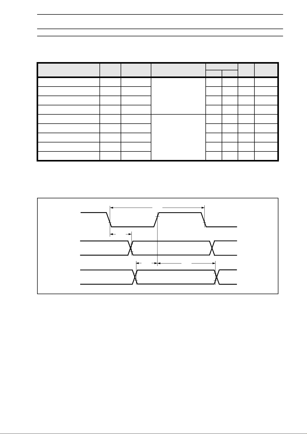
14.9 UART1 Timing
(TA = –40 to +85°C, VCC = 4.5 to 5.5 V, VSS = 0 V)
Parameter Symbol Pin Symbol Test Condition
Serial clock cycle time tSCYC SCK1
SCK ↓ ⇒ SOT delay time tSLOV SCK1, SOT1 –80 80 ns
Valid SIN ⇒ SCK ↑ tIVSH SCK1, SIN1 100 — ns
SCK ↑ ⇒ Valid SIN hold time tSHIX SCK1, SIN1 60 — ns
Internal clock operation
output pins are CL =80pF
+ 1 TTL.
Rated Value
Min. Max.
8 tCP —ns
Units Remarks
Serial clock "H" pulse width tSHSL SCK1
Serial clock "L" pulse width tSLSH SCK1 4 tCP —ns
SCK ↓ ⇒ SOT delay time tSLOV SCK1, SOT1 — 150 ns
Valid SIN ⇒ SCK ↑ tIVSH SCK1, SIN1 60 — ns
SCK ↑ ⇒ Valid SIN hold time tSHIX SCK1, SIN1 60 — ns
Notes:
1. AC characteristic in CLK synchronized mode.
2. CL is load capacity value of pins when testing.
3. tCP is the machine cycle (Unit: ns).
SCK
SOT
0.8 V
tSLOV
2.4 V
0.8 V
External clock operation
output pins are CL =80pF
+ 1 TTL.
tSCYC
2.4 V
tIVSH
tSHIX
4 tCP —ns
0.8 V
SIN
0.8 VCC
0.2 VCC
0.8 VCC
0.2 VCC
Figure 14.10 Internal Shift Clock Mode
MB90495 Series Data Sheet (Advance Information) 33 / 40 FME EMDC June 19, 2000

MB90495 Series
SCK
SOT
SIN
0.2 VCC
tSLOV
tSLSH
0.8 VCC
0.2 VCC
2.4 V
0.8 V
tIVSH
0.8 VCC
0.2 VCC
tSHSL
0.8 VCC
tSHIX
Figure 14.11 External Shift Clock Mode
0.8 VCC
0.2 VCC
MB90495 Series Data Sheet (Advance Information) 34 / 40 FMG EMDC June 19, 2000

14.10 Timer Related Resource Input Timing
Parameter
Input pulse width
Sym-
bol
tTIWH TIN0, TIN1
tTIWL IN0 to IN3
Pin
Test Condi-
tion
—4 tCP —ns
MB90495 Series
(TA = –40 to +85°C, VCC = 4.5 to 5.5 V, VSS = 0 V)
Rated Value
Min. Max.
Unit
s
Remarks
0.8 VCC
tTIWH
0.8 VCC
0.2 VCC
Figure 14.12 Timer Input Timing
0.2 VCC
tTIWL
MB90495 Series Data Sheet (Advance Information) 35 / 40 FME EMDC June 19, 2000

MB90495 Series
14.11 Timer Related Resource Output Timing
Parameter Symbol Pin Test Condition
CLK ↑ ⇒ TOUT change time tTO
TOT0 to TOT1,
PPG0 to PPG3
—30—ns
(TA = –40 to +85°C, VCC = 4.5 to 5.5 V, VSS = 0 V)
Rated Value
Min. Max.
Units Remarks
CLK
OT/PPG
T
2.4 V
2.4 V
0.8 V
tTO
Figure 14.13 Timer Output Timing
MB90495 Series Data Sheet (Advance Information) 36 / 40 FMG EMDC June 19, 2000

14.12 External Trigger Input Timing
Parameter Symbol Pin Test Condition
Input pulse width
tTRGH
tTRGL
INT0to INT7,
ADTG
MB90495 Series
(TA = –40 to +85°C, VCC = 4.5 to 5.5 V, VSS = 0 V)
Rated Value
Min. Max.
—5 tCP —ns
Units Remarks
0.8 VCC
0.8 VCC
0.2 VCC
tTRGH
0.2 VCC
tTRGL
Figure 14.14 External Trigger Input Timing
MB90495 Series Data Sheet (Advance Information) 37 / 40 FME EMDC June 19, 2000

MB90495 Series
14.13 A/D Converter
(TA = –40 to +85°C, 3.0 V ≤ AVR – AVSS, VCC = AVCC = 5.0 V 10%, VSS = AVSS = 0 V)
Parameter Symbol Pin
Resolution — — — 10 bit
Conversion error — — — — 5.0 LSB
Nonlinearity error — — — — 2.5 LSB
Differential nonlinearity error — — — — 1.9 LSB
Min. Typ. Max.
Rated Value
Units Remarks
Zero reading voltage VOT AN0 to AN7 AVSS – 3.5 AVSS +0.5 AVSS + 4.5 LSB
Full scale reading voltage VFST AN0 to AN7 AVR – 6.5 AVR –1.5 AVR + 1.5 LSB
Conversion time — — — 176tCP —ns
Sampling time — — — 64tCP —ns
Analog port input current IAIN AN0 to AN7 — — 10 µA
Analog input voltage range VAIN AN0 to AN7 AVSS — AVR V
Reference voltage range — AVR AVSS + 2.7 — AVCC V
IA AVCC — 5 — mA
Power supply current
IAH AVCC — — 5 µA*1
IR AVR 200 400 600 µA
Reference voltage current
IRH AVR — — 5 µA*1
Offset between input channels — AN0 to AN7 — — 4 LSB
*1: When not operating A/D converter, this is the current (VCC = AVCC = AVR = 5.0 V) when the CPU is stopped.
Terminology:
Conversion error : Absolute maximum conversion deviation with respect to the theoretical conversion line.
Nonlinearlity : Relative maximum conversion deviation with respect to the theoretical conversion line connecting to
the device-unique zero reading voltage and full-scale reading voltage.
Differential non-linearlity : Maximum conversion deviation in any two adjacent reading voltages with respect to the theoretical
LSB conversion step.
Zero-reading voltage : Input voltage which results in the minimum conversion value.
Full-scale reading voltage : Input voltage which results in the maximum coversion value.
1 LSB =
AVR/1024
Notes:
1. The accuracy gets worse as AVR - AVSS becomes smaller.
2. Analog input external circuit output impedance should use the following conditions:
External circuit output impedance less than 15 kΩ
3. If the external circuit output impedance is too high, there may be insufficient time for sampling of the analog voltage.
Converter
C1
Analog input
C0
Figure 14.15 Analog Input pin
MB90495 Series Data Sheet (Advance Information) 38 / 40 FMG EMDC June 19, 2000

15. PACKAGE DIMENSIONS
MB90495 Series
14.00±0.20(.551±.008)SQ
12.00±0.10(.472±.004)SQ
49
1 PIN INDEX
64
LEAD No.
0.65(.0256)TYP 0.30±0.10
116
(.012±.004)
0.10(.004)
C
1994 FUJITSU LIMITED F64018S-1C-2
0.13(.005)
3348
32
17
"A"
M
+0.20
–0.10
1.50
+.008
.059
–.004
9.75 13.00
(.384)
REF
+0.05
–0.02
0.127
+.002
–.001
.005
(Mounting height)
(.512)
NOM
Details of "A" part
0 10°
0.10±0.10
(.004±.004)
0.50±0.20
(.020±.008)
(STAND OFF)
Figure 15.1 Package Code: FPT-64P-M09
MB90495 Series Data Sheet (Advance Information) 39 / 40 FME EMDC June 19, 2000

MB90495 Series
51
64
LEAD No.
24.70±0.40(.972±.016)
20.00±0.20(.787±.008)
INDEX
"A"
1
1.00(.0394) 0.40±0.10
0.10(.004)
18.00(.709)REF
22.30±0.40(.878±.016)
(.016±.004)TYP
0.20(.008)
33
(.551±.008)
19
"B"
3252
14.00±0.20
20
M
Details of "A" part
18.70±0.40
(.736±.016)
0.25(.010)
0.30(.012)
0.18(.007)MAX
0.63(.025)MAX
3.35(.132)MAX
(Mounting height)
0.05(.002)MIN
(STAND OFF)
12.00(.472)
REF
0.15±0.05(.006±.002)
Details of "B" part
16.30±0.40
(.642±.016)
0 10°
1.20±0.20
(.047±.008)
C
1994 FUJITSU LIMITED F64013S-3C-2
Figure 15.2 Package Code FPT-64P-M06
MB90495 Series Data Sheet (Advance Information) 40 / 40 FMG EMDC June 19, 2000
 Loading...