

Page 1

查询MB90497G供应商
FUJITSU SEMICONDUCTOR
DATA SHEET
16-bit Proprietary Microcontroller
CMOS
F2MC-16LX MB90495G Series
MB90497G/F497G/F498G/V495G
DESCRIPTION
■
The MB90495G Series is a general-purpose, high-performance 16-bit microcontroller. It was designed f or devices
like consumer electronics, which require high-speed, real-time process control. This series features an on-chip
full-CAN interface.
In addition to being backwards compatible with the F
panded to add support for high-level language instructions, e xpanded addressing mode, and enhanced multiply/
divide and bit processing instructions. A 32-bit accumulator is also provided, making it possible to process long
word (32-bit) data.
2
MC* family architecture, the instruction set has been ex-
DS07-13713-3E
The MB90495G Series peripheral resources include on chip 8/10-bit A/D converter, UART (SCI) 0/1, 8/16-bit
PPG timer, 16-bit I/O timer (16-bit free-run timer, input capture 0, 1, 2, 3 (ICU) ) , and CAN controller.
2
* : F
MC is abbreviation for Fujitsu Flexible Microcontroller. F2MC is a registered trademark of Fujitsu Limited.
FEATURES
■
• Models that support +125 °C
•Clock
•Built-in PLL clock multiplier circuit
•Choose 1/2 oscillation clock or ×1 to ×4 multiplied oscillation clock (f or a 4-MHz oscillation cloc k, 4 to 16 MHz)
machine (PLL) clock
(Continued)
PACKAGES
■
64-pin plastic QFP 64-pin plastic LQFP
(FPT-64P-M06) (FPT-64P-M09)
Page 2

MB90495G Series
(Continued)
•Select subclock behavior (8.192 kHz)
•Minimum instruction execution time : 62.5 ns (operating with 4-MHz oscillation clock and × 4 PLL clock)
• 16-MByte CPU memory space
•24-bit internal addressing
•External access possible through selection of 8/16-bit bus width (external bus mode)
• Optimum instruction set for controller applications
•Wealth of data types (Bit, Byte, Word, Long Word)
•Wealth of addressing modes (23 different modes)
•Enhanced signed multiply-divide instructions and RETI instruction functions
•Enhanced high-precision arithmetic employing 32-bit accumulator
• Instruction set supports high-level programming language (C) and multitasking
•Employs system stack pointer
•Enhanced indirect instructions with all pointer types
•Barrel shift instructions
• Improved execution speed
•4-byte instruction queue
• Powerful interrupt feature
•Powerful 8-level, 34-condition interrupt feature
• CPU-independent automated data forwarding
2
•Extended intelligent I/O service feature (EI
• Low-power consumption (Standby) Mode
•Sleep mode (CPU operation clock stopped)
•Time-base timer mode (oscillation clock and subclock, time-base timer and watch timer only operational)
•Watch mode (subclock and watch timer only operational)
•Stop mode (oscillation clock and subclock stopped)
•CPU intermittent operation mode
• Process
•CMOS technology
• I/O Ports
•Generic I/O ports (CMOS output) : 49
•Timer
•Time-base timer, watch timer, watchdog timer : 1 channel
•8/16-bit PPG timer : four 8-bit channels, or two 16-bit channels
•16-bit reload timer : 2 channels
•16-bit I/O timer
•16-bit free-run timer : 1 channel
•16-bit input capture (ICU) : 4 channels
Generates interrupt requests by latching onto the count value of the 16-bit free-run timer with pin input
edge detection
OS) : maximum 16 channels
(Continued)
2
Page 3

MB90495G Series
(Continued)
•
CAN Controller
•CAN specifications conform to versions 2.0A and 2.0B
•8 on-chip message buffers
•Forwarding rate 10 Kbps to 1 Mbps (with 16-MHz machine clock)
• UART0 (SCI) /UART1 (SCI) : 2 channels
•All with full duplex double buffer
•Use clock-asynchronous or clock-synchronous serial forwarding
• DTP/external interrupt : 8 channels
•A module for launching extended intelligent I/O service (EI
external output
• Delayed interrupt generation module
•Generates interrupt requests for switching tasks
• 8/10-bit A/D converter : 8 channels
•Switch between 8-bit and 10-bit resolution
•Launch through external trigger input
•Conversion time : 6.13 µs (with 16-MHz machine clock, including sampling time)
:
1 channel
2
OS) and generating external interrupts through
• Program batch function
•2-address pointer ROM correction
• Clock output function
3
Page 4

MB90495G Series
PRODUCT LINEUP
■
Part Number
Paarmeter
Feature Classification FLASH ROM Mask ROM FLASH ROM Product Evaluated
ROM Size 64 Kbytes 128 Kbytes
RAM Size 2 Kbytes 6 Kbytes
Process CMOS
Package LQFP64 (width 0.65 mm) , QFP64 (width 1.0 mm) PGA256
Operating Power 4.5 V to 5.5 V
Emulator power supply* None
CPU Functions
Low-power consumption
(Standby) Mode
I/O Ports General-purpose I/O ports (CMOS output) : 49
Time-base timer
Watchdog timer
MB90F497G MB90497G MB90F498G MB90V495G
Number of instructions
Instruction bit length
Instruction length
Data bit length
Minimum execution time : 62.5 ns (with 16-MHz machine clock)
Interrupt processing time : minimum 1.5 µs (with 16-MHz machine clock)
Sleep mode/watch mode/time-base timer mode/stop mode / CPU intermittent
mode
18-bit free-run counter
Interrupt interval : 1.024 ms, 4.096 ms, 16.834 ms, 131.072 ms
(with 4-MHz oscillation clock)
Reset generation intervals : 3.58 ms, 14.33 ms, 57.23 ms, 458.75 ms
(with 4-MHz oscillation clock)
: 351
: 8-bit, 16-bit
: 1 to 7 bytes
: 1 bit, 8-bit, 16-bit
16-bit
free-run timer
16-bit
I/O Timer
Input capture
16-bit reload timer
Watch timer
8/16-bit PPG timer
* : The S2 dipswitch setting when using the MB2145-507 emulation baud. For details, see the MB2145-507
hardware manual (2.7 Emulator Power Pin) .
4
Number of channels : 1
Interrupts from overflow generation
Number of channels : 4
Maintenance of free-run timer value through pin input (rising, falling or both edges)
Number of channels : 2
16-bit reload timer operation
Count clock interval : 0.25 µs, 0.5 µs, 2.0 µs
(with 16-MHz machine clock)
External event count enabled
15-bit free-run counter
Interrupt intervals : 31.25 ms, 62.5 ms, 12 ms, 250 ms, 500 ms, 1.0 s, 2.0 s
(with 8.192-kHz subclock)
Number of channels : 2 (two 8-bit channels can be used)
Two 8-bit or one 16-bit channel PPG operation possible
Free interval, free duty pulse output possible
Count clock : 62.5 ns to 1 µs (with 16-MHz machine clock)
(Continued)
Page 5

(Continued)
Part Number
Parameter
Delayed interrupt generation
module
DTP/external interrupt circuit
8/10-bit A/D converter
UART0 (SCI)
UART1 (SCI)
CAN
MB90495G Series
MB90F497G MB90497G MB90F498G MB90V495G
Module for delayed interrupt generation switching tasks
Used in real-time OS
Number of inputs : 8
Starting by rising edge, falling edge, “H” level input, or “L” level input, external
interrupts or extended intelligent I/O service (EI
Number of channels : 8
Resolution : set 10-bit or 8-bit
Conversion time : 6.13 µs (with 16-MHz machine clock, including sampling time)
Continuous conversion of multiple linked channels possible
(up to 8 channels can be set)
One-shot conversion mode : converts selected channel only once
Continuous conversion mode : converts selected channel continuously
Stop conversion mode : converts selected channel and suspends operation
repeatedly
Number of channels : 1
Clock-synchronous forwarding : 62.5 Kbps to 2 Mbps
Clock-asynchronous forwarding : 1,202 bps to 62,500 bps
Transmission can be performed by two-way serial transmission or by master/
slave connection
Number of channels : 1
Clock-synchronous forwarding : 62.5 Kbps to 2 Mbps
Clock-asynchronous forwarding : 9,615 bps to 500 Kbps
Transmission can be performed by two-way serial transmission or by master/
slave connection
Compliant with CAN specification versions 2.0A and 2.0B
Send/receive message buffers : 8
Forwarding bit rate : 10 Kbps to 1 Mbps (with 16-MHz machine clock)
2
OS) can be used
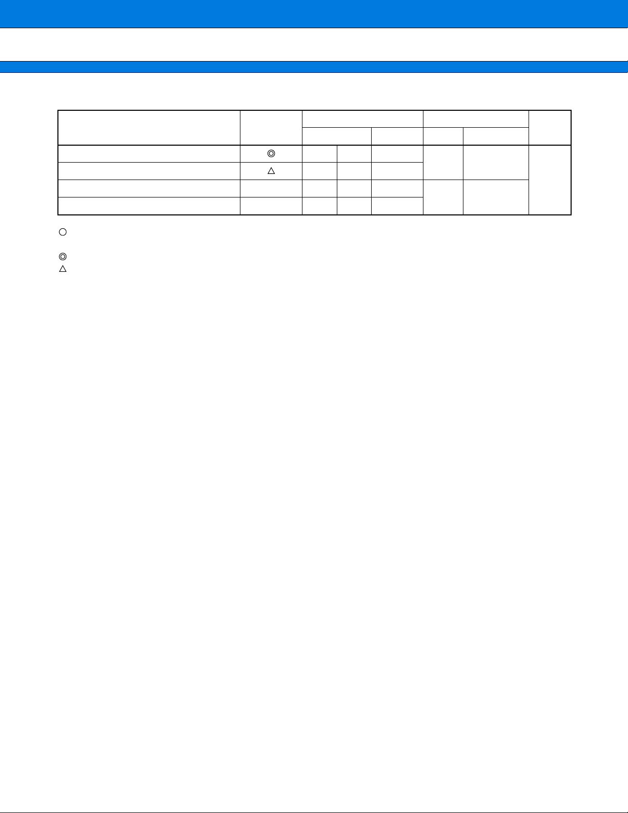
PACKAGES AND CORRESPONDING PRODUCTS
■
Package MB90F497G MB90497G MB90F498G
FPT-64P-M06
FPT-64P-M09
: available × : not available
Note : See “Package Dimensions” for details.
PRODUCT COMPARISON
■
Memory Size
When evaluating with e valuation chips and other means, tak e careful note of the different between the e valuation
chip and the chip actually used. Take particular note of the following.
• While the MB90V495G does not feature an on-chip ROM, the dedicated development tool can be used to
achieve operation equivalent to a product with built-in ROM. Therefore, the ROM size is configured by the
development tool.
• On the MB90V495G, the FF4000
FF3FFF
• On the MB90F497G/F498G/497G, the FF4000
to FF3FFFH is visible only in the FF bank.
H is only visible in the FE and FF banks (configurable on development tool) .
H to FFFFFFH image is only visible in the 00 bank, and the FE0000H to
H to FFFFFFH image is visible in the 00 bank, and the FF0000H
5
Page 6

MB90495G Series
PIN ASSIGNMENTS
■
• FPT-64P-M06
SS
P27/INT7/A23
P30/SOT0/ALE
V
(TOP VIEW)
P26/INT6/A22
P25/INT5/A21
P24/INT4/A20
P23/TOT1/A19
P22/TIN1/A18
P21/TOT0/A17
P20/TIN0/A16
P17/PPG3/AD15
P16/PPG2/AD14
P15/PPG1/AD13
P14/PPG0/AD12
P13/IN3/AD11
P12/IN2/AD10
P11/IN1/AD09
P10/IN0/AD08
P07/AD07
P31/SCK0/RD
P32/SIN0/WRL
P33/WRH
P34/HRQ
P35/HAK
V
CC
P36/FRCK/RDY
P37/ADTG/CLK
P40/SIN1
P41/SCK1
P42/SOT1
P43/TX
51
52
58
C
64
1
P44/RX
P50/AN0
P51/AN1
P61/INT1
P62/INT2
P52/AN2
P53/AN3
P54/AN4
P55/AN5
42
10
CC
AV
P56/AN6
P57/AN7
AVR
SS
AV
P60/INT0
X0A
X1A
P63/INT3
33
32
26
20
19
MD0
P06/AD06
P05/AD05
P04/AD04
P03/AD03
P02/AD02
P01/AD01
P00/AD00
V
SS
X1
X0
MD2
MD1
RST
(FPT-64P-M06)
6
Page 7

• FPT-64P-M09
(TOP VIEW)
P27/INT7/A23
P26/INT6/A22
P25/INT5/A21
P24/INT4/A20
P23/TOT1/A19
P22/TIN1/A18
P21/TOT0/A17
P20/TIN0/A16
P17/PPG3/AD15
P16/PPG2/AD14
MB90495G Series
P15/PPG1/AD13
P14/PPG0/AD12
P13/IN3/AD11
P12/IN2/AD10
P11/IN1/AD09
P10/IN0/AD08
V
P30/SOT0/ALE
P31/SCK0/RD
P32/SIN0/WRL
P33/WRH
P34/HRQ
P35/HAK
V
P36/FRCK/RDY
P37/ADTG/CLK
P40/SIN1
P41/SCK1
P42/SOT1
P43/TX
P44/RX
SS
CC
48
49
57
C
64
1
P50/AN0
P51/AN1
P52/AN2
P61/INT1
P62/INT2
P53/AN3
40
8
P54/AN4
P55/AN5
P56/AN6
CC
AVR
AV
P57/AN7
SS
AV
P60/INT0
X0A
33
16
X1A
32
24
17
P07/AD07
P06/AD06
P05/AD05
P04/AD04
P03/AD03
P02/AD02
P01/AD01
P00/AD00
SS
V
X1
X0
MD2
MD1
RST
MD0
P63/INT3
(FPT-64P-M09)
7
Page 8

MB90495G Series
PIN DESCRIPTION
■
Pin No.
Pin Name
M06 M09
P61
21
INT1 Functions as external interrupt input pin. Set this to input port.
P62
32
INT2 Functions as external interrupt input pin. Set this to input port.
P50 to P57
4 to 11 3 to 10
AN0 to
AN7
12 11 AV
CC VCC power input pin of A/D converter.
13 12 AVR
14 13 AV
SS VSS power input pin of A/D converter.
P60
15 14
INT0 Functions as external interrupt input pin. Set this to input port.
16 15 X0A A
17 16 X1A A
Circuit
Type
D
D
E
D
Description
General-purpose I/O port
General-purpose I/O port
General-purpose I/O port
Functions as analog input port of A/D converter. This is enabled if analog
input configuration is permitted.
Reference voltage (+) input pin for the A/D converter.This voltage must
not exceed V
CC and AVCC. Reference voltage (−) is fixed to AVSS.
General-purpose I/O port
Low-speed oscillation pin.
Perform pull-down processing if not connected to an oscillator.
Low-speed oscillation pin.
Set to open if not connected to an oscillator.
18 17
P63
General-purpose I/O port
D
INT3 Functions as external interrupt input pin. Set this to input port.
19 18 MD0 C Input pin for specifying operation mode.
20 19 RST
B External reset input pin.
21 20 MD1 C Input pin for specifying operation mode.
22 21 MD2 F Input pin for specifying operation mode.
23 22 X0 A High-speed oscillation pin.
24 23 X1 A High-speed oscillation pin.
25 24 V
26 to 3325 to
32
34 to 3733 to
36
SS Power supply (0 V) input pin.
P00 to P07
General-purpose I/O port
Only enabled in single-chip mode.
D
AD00 to
AD07
P10 to P13
IN0 to IN3
AD08 to
AD11
I/O pin for the lower 8-bit of the external address data bus.
Only enabled during external bus mode.
General-purpose I/O port. Only enabled in single-chip mode.
Functions as trigger input pin for input capture channels 0 to 3. Set this to
D
input port.
I/O pin for upper 4-bit of external address data bus.
Only enabled during external bus mode.
(Continued)
8
Page 9

(Continued)
Pin No.
M06 M09
38 to 4137 to
40
Pin Name
P14 to P17
PPG0 to
PPG3
Circuit
Type
D
MB90495G Series
Description
General-purpose I/O port.
Only enabled in single-chip mode.
Functions as output pin of PPG timer 01, 23. Only valid if output configuration is enabled.
42 41
43 42
AD12 to
AD15
P20
TIN0
A16
P21
TOT0
A17
P22
I/O pin for upper 4-bit of external address data bus.
Only enabled during external bus mode.
General-purpose I/O port.
When the bits of high address control register (HACR) are set to “1” in external bus mode, these pins function as general purpose I/O ports.
Functions as event input pin of TIN0 reload timer 0.
D
Set this to input port.
Output pin of external address bus (A16) .
Only valid when the bits of high address control register (HACR) are set
to “0” in external bus mode.
General-purpose I/O port.
When the bits of high address control register (HACR) are set to “1” in external bus mode, these pins function as general purpose I/O ports.
Functions as event output pin of TOT0 reload timer 0.
D
Only valid if output configuration enabled.
Output pin of external address bus (A17) .
Only valid when the bits of high address control register (HACR) are set
to “0” in external bus mode.
General-purpose I/O port.
When the bits of high address control register (HACR) are set to “1” in external bus mode, these pins function as general purpose I/O ports.
44 43
45 44
TIN1
A18
P23
TOT1
A19
Functions as event input pin of TIN1 reload timer 1.
D
Set this to input port.
Output pin of external address bus (A18) .
Only valid when the bits of high address control register (HACR) are set
to “0” in external bus mode.
General-purpose I/O port.
When the bits of high address control register (HACR) are set to “1” in external bus mode, these pins function as general purpose I/O ports.
Functions as event output pin for TOT1 reload timer 1.
D
Only valid if output configuration enabled.
Output pin for external address bus (A19) .
Only valid when the bits of high address control register (HACR) are set
to “0” in external bus mode.
(Continued)
9
Page 10

MB90495G Series
(Continued)
Pin No.
M06 M09
46 to 4945 to
48
Pin Name
P24 to P27
INT4 to INT7
A20 to A23
Circuit
Type
D
Description
General-purpose I/O port.
When the bits of high address control register (HACR) are set to “1” in external bus mode, these pins function as general purpose I/O ports.
Functions as external interrupt input pin. Set this to input port.
Output pin for external address bus (A20 to A23) .
Only valid when the bits of high address control register (HACR) are set
to “0” in external bus mode.
50 49 V
P30
51 50
52 51
53 52
54 53
SOT0
ALE
P31
SCK0
P32
SIN0
WRL
P33
WRH
SS Power supply (0 V) input pin.
General-purpose I/O port.
Only enabled in single-chip mode.
UART0 serial data output pin.
D
Only valid if UART0 serial data output configuration is enabled.
Address latch authorization output pin.
Only enabled during external bus mode.
General-purpose I/O port.
Only enabled in single-chip mode.
UART0 serial clock I/O pin.
D
Only valid if UART0 serial clock I/O configuration is enabled.
RD
Lead strobe output pin.
Only enabled during external bus mode.
General-purpose I/O port.
UART0 serial data input pin.
D
Set this to input port.
Write strobe output pin for lower 8-bit of data bus.
Only valid if WRL
General-purpose I/O port.
D
Write strobe output pin for upper 8-bit of data bus.
Only valid if external bus mode/16-bit bus mode/WRH
pin output is enabled, in external bus mode.
pin output enabled.
55 54
56 55
57 56 V
58 57 C
10
P34
HRQ
P35
HAK
CC Power supply (5 V) input pin.
General-purpose I/O port.
D
Hold request input pin.
Only valid if hold input is enabled, in external bus mode.
General-purpose I/O port.
D
Hold addressing output pin.
Only valid if hold input is enabled, in external bus mode.
Capacity pin for power stabilization.
Please connect to an approximately 0.1 µF ceramic capacitor.
(Continued)
Page 11

(Continued)
Pin No.
M06 M09
Pin Name
P36
Circuit
Type
MB90495G Series
Description
General-purpose I/O port.
59 58
60 59
61 60
62 61
63 62
64 63
164
FRCK
RDY
P37
ADTG Functions as A/D converter external trigger input pin. Set this to input port.
CLK
P40
SIN1
P41
SCK1
P42
SOT1
P43
TX
P44
RX
Functions as an external clock input pin for a FRCK 16-bit free-run timer.
D
Set this to input port.
External ready input pin.
Only valid if external ready input is enabled, in external bus mode.
General-purpose I/O port.
D
External clock output pin.
Only valid if external clock output is enabled, in external bus mode.
General-purpose I/O port.
D
UART1 serial data input pin.
Set this to input port.
General-purpose I/O port.
D
UART1 serial clock I/O pin.
Only valid if UART1 clock I/O configuration is enabled.
General-purpose I/O port.
D
UART1 serial data output pin.
Only valid if UART1 serial data output configuration is enabled.
General-purpose I/O port.
D
CAN transmission output pin.
Only valid if output configuration enabled.
General-purpose I/O port.
D
CAN reception input pin.
Set this to input port.
11
Page 12

MB90495G Series
I/O CIRCUIT TYPE
■
Type Circuit Remarks
X1
Clock input
X1A
• High speed oscillation feedback
resistor : 1 MΩ approx.
• Low speed oscillation feedback
resistor : 10 MΩ approx.
A
X0
X0A
Standby control signal
• Hysteresis input with pull-up
VCC
B
R
R
Hysteresis input
• Pull-up Resistor : 50 kΩ approx.
• Hysteresis input
C
R
Hysteresis input
• CMOS hysteresis input
CC
V
Pch
Digital output
D
V
R
IOL = 4 mA
SS
Standby control
Nch
Digital output
Hysteresis input
• CMOS level output
• Standby control available
12
CC
V
Pch
Digital output
• CMOS level output
• Doubles as analog input pin
• Standby control available
• CMOS hysteresis input
E
R
IOL = 4 mA
Nch
V
SS
Standby control
Analog input
Digital output
Hysteresis input
(Continued)
Page 13

MB90495G Series
(Continued)
Type Circuit Remarks
R
F
R
V
SS
Hysteresis input
• Pull-down Resistor : 50 kΩ approx.
(except FLASH device)
• Hysteresis input with pull-down
13
Page 14

MB90495G Series
HANDLING DEVICES
■
• Make sure you do not exceed the maximum rated values (in order to prevent latch-up) .
• CMOS IC chips may suffer latch-up if a voltage higher than V
output pin with other than mid or high current resistance; or voltage exceeding the r ating is applied across VCC
and V
SS.
• Latch-ups can dramatically increase the power supply current, causing thermal breakdown of the device.
Make sure that you do not exceed the maximum rated value of your device, in order to prevent a latch-up.
• When turning the analog power supply on or off, make sure that the analog power v oltage (AV
analog input voltages do not exceed the digital voltage (VCC) .
• Handling Unused Pins
Leaving unused input pins open may cause malfunctions and latch-ups, per manently damaging the device.
Prevent this by connecting it to a pull-up or pull-down resistor of no less than 2 kΩ. Leave unused output pins
open in output mode, or if in input mode, handle them in the same as input pins.
• Notes on Using External Clock
When using the external clock, drive pin X0 only, and leave pin X1 unconnected. See below for an example of
external clock use.
CC or lower than VSS is applied to an input or
CC, A VR) and
Example External Clock Use
X0
Open
X1
MB90495G Series
• Notes on Not Using Subclock
If you do not connect pins X0A and X1A to an oscillator, use pull-down handling on the X0A pin, and leave the
X1A pin open.
•Power Supply Pins
• If your product has multiple V
CC or VSS pins, pins of the same potential are internally connected in the device
in order to avoid abnormal operation, including latch-up . Howe ver, you should mak e sure to connect the pins’
external power and ground lines, in order to low er unneeded emissions, prevent abnormal operation of strobe
signals due to a rise in ground levels, and maintain total output current within rated levels.
• T ak e care to connect the V
CC and VSS pins of MB90495G Series devices to power lines via the low est possible
impedance.
• It is recommended that you connect a bypass capacitor of approximately 0.1 µF between V
CC and VSS near
MB90495G Series device pins.
• Crystal Oscillator Circuit
• Noise in the vicinity of X0 and X1 pins could cause abnormal operations in MB90495G Series devices. Make
sure to provide bypass capacitors via the shortest possible distance from X0 and X1 pins, crystal oscillators
(or ceramic resonators) , and ground lines. In addition, design your printed circuit boards so as to keep X0
and X1 wiring from crossing other wiring, if at all possible.
• It is strongly recommended that you provide printed circuit board artwork surrounding X0 and X1 pins within
a grand area, as this should stabilize operation.
14
Page 15

MB90495G Series
• A/D Converter Power-up and Analog Input Initiation Sequence
• Make sure to power up the A/D con verter and analog input (pins AN0 to AN7) after turning on digital power
(V
CC) .
• Turn off digital power after turning off the A/D converter power supply and analog inputs. In this case, make
sure that the voltage of AVR does not exceed AV
simultaneously) .
• Connecting Unused A/D Converter Pins
CC (it is permissible to turn off analog and digital power
If you are not using the A/D converter, set unused pins to AV
CC = AVR = VCC, AVSS = VSS.
• Notes for Powering Up
Ensure that the voltage step-up time (between 0.2 V and 2.7 V) at power-up is no less than 50 µs, in order to
prevent malfunction in the built-in step-down circuit.
• Initialization
The device contains built-in registers which are only initialized by a power-on reset. Cycle the power supply to
initialize these registers.
• Stabilizing the Power Supply
Make sure that the V
CC power supply voltage is stable. Even at the rated operating VCC power supply voltage,
large, sudden changes in the voltage could cause malfunctions. As a standard for stable power supply, keep
V
CC ripples (peak-to-peak value) at commercial power frequencies (50 Hz to 60 Hz) to no more than 10% of the
power supply voltage, and momentary surges caused by switching the power supply and other events to more
than 0.1 V/ms.
• If Output from Ports 0/1 Becomes Undefined
After power is turned on, if the RST
on reset) , ports 0 and 1 output will be undefined. If the RST
pin is set to “H” during step-down circuit stabilization standby (during power-
pin is set to “L”, ports 0 and 1 will go into a high
impedance state. Take careful note of the timing of events outlined in figures 1 and 2.
15
Page 16

MB90495G Series
•
Figure 1 - Timing Chart of Undefined Output from Ports 0/1 (with RST
Time in standby for oscillation to stabilize
VCC (power supply pin)
PONR (power-on reset) signal
RST (external asynchronous reset) signal
RST (internal reset) signal
Oscillation clock signal
KA (internal operating clock A) signal
KB (internal operating clock B) signal
PORT (port output) signal
Time in standby for stepdown circuit to stabilize
Time of undefined output
1
*
pin set to “H
*1 : Step-down circuit stabilization standby time : 217/oscillation clock frequency
(with 16-MHz oscillation clock frequency, about 8.19 ms)
*2 : Oscillation stabilization standby time : 2
18
/oscillation clock frequency
(with 16-MHz oscillation clock frequency, about 16.36 ms)
”)
2
*
•
Figure 2 - Timing Chart of High Impedance State for Ports 0/1 (when RST
Time in standby for oscillation to stabilize
VCC (power supply pin)
PONR (power-on reset) signal
RST (external asynchronous reset) signal
RST (internal reset) signal
Oscillation clock signal
KA (internal operation clock A) signal
KB (internal operating clock B) signal
PORT (port output) signal
Step-down circuit
stabilization standby time
High impedance
1
*
*1 : Step-down circuit stabilization standby time : 217/oscillation clock frequency
(with 16-MHz oscillation clock frequency, about 8.19 ms)
*2 : Oscillation stabilization standby time : 2
18
/oscillation clock frequency
(with 16-MHz oscillation clock frequency, about 16.38 ms)
pin is “L
2
*
”)
16
Page 17

MB90495G Series
• Caution on Operations during PLL Clock Mode
If the PLL clock mode is selected in the microcontroller , it may attempt to continue the operation using the freerunning frequency of the automatic oscillating circuit in the PLL circuitry even if the oscillator is out of place or
the clock input is stopped. Performance of this operation, however, cannot be guaranteed.
++++
• Support for
125
°°°°
C
If used exceeding T
A = +105 °C, be sure to contact us for reliability limitations.
17
Page 18

MB90495G Series
BLOCK DIAGRAM
■
X0, X1
RST
X0A, X1A
SOT1
SCK1
SIN1
SOT0
SCK0
SIN0
Clock
control circuit
Watch timer
Time-base timer
RAM
ROM/FLASH
Prescaler
UART1
Prescaler
UART0
CPU
2
F
MC-16LX
Core
16 bit
free-run timer
Input
capture
(4 ch)
16-bit
PPG timer
(2 ch)
Internal data bus
CAN
DTP/external
interrupt circuit
16 bits
reload timer
(2 ch)
FRCK
IN0 to IN3
PPG0 to PPG3
RX
TX
INT0 to INT7
TIN0, TIN1
TOT0, TOT1
18
AV
CC
AVSS
AN0 to AN7
AVR
ADTG
8/10 bit
A/D converter
(8 ch)
External bus
AD00 to AD15
A16 to A23
ALE
RD
WRL
WRH
HRQ
HAK
RDY
CLK
Page 19

MB90495G Series
MEMORY MAP
■
The memory access modes of the MB90495G Series can be set to single chip mode, internal ROM - exter n al
bus mode, and external ROM - external bus mode.
1. Memory Allocation of the MB90495G
The MB90495G Series has 24-bit internal address bus and 24-bit external address bus output, enabling it to
access up to 16 Mbytes of external access memory . The enable/disab le time of the ROM mirror function is shown
graphically in the memory map.
2. Memory Map
000000H
0000C0H
000100H
Address #1
002000H
003800
H
003900H
Address #2
010000H
Address #3
FFFFFFH
Single chip mode
(ROM mirror function available)
Periphery Periphery Periphery
RAM space
Register
Extention
IO space
ROM space
(image of
bank FF)
ROM space
Internal access memory
External access memory
Access prohibited
Internal ROM
External bus mode
RAM space
Register
Extention
IO space
ROM space
(image of
bank FF)
ROM space
External ROM
External bus mode
RAM space
Register
Extention
IO space
Product
Address #1
MB90V495G 001900
*
H 004000H (FC0000H)
Address #2 Address #3
*
MB90F497G 000900H 004000H FF0000H
MB90497G 000900H 004000H FF0000H
MB90F498G 000900H 004000H FE0000H
* : Addresses #1 and #3 are product-specific.
Note : When the internal ROM is operational, the ROM data in the upper address of bank 00 of the F2MC-16LX is
visible in an image. This is called the ROM mirror function, and tak es advantage of the small C compiler model.
With the F
2
MC-16LX, the lower 16-bit address of bank FF and the lower 16-bit address of bank 00 are set
identical to one another. This allo ws the ROM-internal table to be ref erenced without specifying a far pointer .
For e xample, sa y the address “00C000
H” is accessed. In actuality, the “FFC000H ” address inside ROM will
be accessed. Howev er, as the ROM space in bank FF exceeds 48 Kb ytes, the entire space cannot be viewed
on bank 00’s image. And so, since “FF4000
“00FFFF
H” image, save the ROM data table in the “FF4000H” to “FFFFFFH” space.
H” to “FFFFFFH” ROM data will be visible on the “004000H” to
19
Page 20

MB90495G Series
I/O MAP
■
Address
000000
Register
Abbreviation
H PDR0 Port 0 data register R/W Port 0 XXXXXXXXB
Register Name Access Resource Name Initial Value
000001H PDR1 Port 1 data register R/W Port 1 XXXXXXXXB
000002H PDR2 Port 2 data register R/W Port 2 XXXXXXXXB
000003H PDR3 Port 3 data register R/W Port 3 XXXXXXXXB
000004H PDR4 Port 4 data register R/W Port 4 XXXXXXXXB
000005H PDR5 Port 5 data register R/W Port 5 XXXXXXXXB
000006H PDR6 Port 6 data register R/W Port 6 XXXXXXXXB
000007H
to
00000F
000010
H
H DDR0 Port 0 direction register R/W Port 0 0 0 0 0 0 0 0 0B
(system-reserved area) *
000011H DDR1 Port 1 direction register R/W Port 1 0 0 0 0 0 0 0 0B
000012H DDR2 Port 2 direction register R/W Port 2 0 0 0 0 0 0 0 0B
000013H DDR3 Port 3 direction register R/W Port 3 0 0 0 0 0 0 0 0B
000014H DDR4 Port 4 direction register R/W Port 4 XXX 0 0 0 0 0B
000015H DDR5 Port 5 direction register R/W Port 5 0 0 0 0 0 0 0 0B
000016H DDR6 Port 6 direction register R/W Port 6 XXXX 0 0 0 0B
000017H
to
00001A
00001B
H
H ADER Analog input enable register R/W
(system-reserved area) *
8/10-bit
A/D converter
1 1 1 1 1 1 1 1B
00001CH
to
00001F
000020
H
H SMR0 Serial mode register 0 R/W
(system-reserved area) *
0 0 0 0 0 0 0 0B
000021H SCR0 Serial control register 0 R/W 0 0 0 0 0 1 0 0B
000022H
SIDR0/
SODR0
Serial input data register 0/
Serial output data register 0
R/W XXXXXXXXB
UART0
000023H SSR0 Serial status register 0 R/W 0 0 0 0 1 X 0 0B
000024H CDCR0
Communication prescaler control
register 0
R/W 0 XXX 1 1 1 1B
000025H SES0 Serial edge selection register 0 R/W XXXXXXX 0B
000026H SMR1 Serial mode register 1 R/W
000027H SCR1 Serial control register 1 R/W 0 0 0 0 0 1 0 0B
000028H
SIDR1/
SODR1
Serial input data register 1/
Serial output data register 1
R/W XXXXXXXXB
UART1
0 0 0 0 0 0 0 0B
20
(Continued)
Page 21

(Continued)
Address
000029
Register
Abbreviation
H SSR1 Serial status register 1 R/W UART1 0 0 0 0 1 0 0 0B
Register Name Access Resource Name Initial Value
00002AH (system-reserved area) *
MB90495G Series
00002B
H CDCR1
Communication prescaler control
register 1
R/W UART1 0 XXX 0 0 0 0B
00002CH
to
00002F
H
000030H ENIR DTP/external interrupt enable register R/W
000031H EIRR
DTP/external interrupt condition
register
(system-reserved area) *
R/W XXXXXXXXB
0 0 0 0 0 0 0 0B
DTP/external
interrupt
000032H
R/W 0 0 0 0 0 0 0 0
ELVR Detection level configuration register
000033H R/W 0 0 0 0 0 0 0 0B
000034H
R/W
0 0 0 0 0 0 0 0
ADCS A/D control status register
000035H R/W 0 0 0 0 0 0 0 0B
000036H
R XXXXXXXX
8/10-bit
A/D converter
ADCR A/D data register
000037H R/W 0 0 1 0 1 XXXB
000038H
to
00003F
000040
H
H PPGC0 PPG0 operation mode control register R/W
000041H PPGC1 PPG1 operation mode control register R/W 0 X 0 0 0 0 0 1B
(system-reserved area) *
0 X 0 0 0 XX 1B
8/16-bit
PPG timer 0/1
000042H PPG01 PPG0/1 count clock selection register R/W 0 0 0 0 0 0 XXB
B
B
B
000043H (system-reserved area) *
000044H PPGC2 PPG2 operation mode control register R/W
000045H PPGC3 PPG3 operation mode control register R/W 0 X 0 0 0 0 0 1B
8/16-bit
PPG timer 2/3
0 X 0 0 0 XX 1B
000046H PPG23 PPG2/3 count clock selection register R/W 0 0 0 0 0 0 XXB
000047H
to
00004F
000050
H
H
(system-reserved area) *
XXXXXXXX
IPCP0 Input capture data register 0 R
000051H XXXXXXXXB
000052H
XXXXXXXX
IPCP1 Input capture data register 1 R
000053H XXXXXXXXB
16-bit I/O timer
000054H ICS01
0 0 0 0 0 0 0 0B
Input capture control status register R/W
000055H ICS23 0 0 0 0 0 0 0 0B
000056H
0 0 0 0 0 0 0 0
TCDT Timer counter data register R/W
000057H 0 0 0 0 0 0 0 0B
(Continued)
B
B
B
21
Page 22

MB90495G Series
(Continued)
Address
000058
000059H 0 XXXXXXXB
Register
Abbreviation
H
Register Name Access Resource Name Initial Value
TCCS Timer counter control status register R/W
0 0 0 0 0 0 0 0
B
00005AH
IPCP2 Input capture data register 2 R
16-bit I/O timer
XXXXXXXX
00005BH XXXXXXXXB
00005CH
XXXXXXXX
IPCP3 Input capture data register 3 R
00005DH XXXXXXXXB
00005EH
to
000065
000066H
H
TMCSR0
(system-reserved area) *
R/W
16-bit reload timer 0
0 0 0 0 0 0 0 0
000067H R/W XXXX0 0 0 0B
Timer control status register
000068H
TMCSR1
R/W
16-bit reload timer 1
0 0 0 0 0 0 0 0
000069H R/W XXXX0 0 0 0B
00006AH
to
00006E
00006F
H
H ROMM ROM mirror function selection register W
(system-reserved area) *
ROM mirror function
selection module
XXXXXXX 1B
000070H
to
00007F
H
(system-reserved area) *
000080H BVALR Message buffer valid register R/W CAN controller 0 0 0 0 0 0 0 0B
B
B
B
B
000081H (system-reserved area) *
000082
H TREQR Send request register R/W CAN controller 0 0 0 0 0 0 0 0B
000083H (system-reserved area) *
000084
H TCANR Send cancel register W CAN controller 0 0 0 0 0 0 0 0B
000085H (system-reserved area) *
000086H TCR Send complete register R/W CAN controller 0 0 0 0 0 0 0 0B
000087H (system-reserved area) *
000088
H RCR Reception complete register R/W CAN controller 0 0 0 0 0 0 0 0B
000089H (system-reserved area) *
00008A
H RRTRR Reception RTR register R/W CAN controller 0 0 0 0 0 0 0 0B
00008BH (system-reserved area) *
00008C
H ROVRR Reception overrun register R/W CAN controller 0 0 0 0 0 0 0 0B
00008DH (system-reserved area) *
00008E
H RIER
Reception complete interrupt enable
register
R/W CAN controller 0 0 0 0 0 0 0 0B
(Continued)
22
Page 23

(Continued)
Address
00008F
H
to
00009D
00009E
H
H PACSR Address detection control register R/W
Register
Abbreviation
MB90495G Series
Register Name Access Resource Name Initial Value
(system-reserved area) *
ROM correction
function
0 0 0 0 0 0 0 0B
00009FH DIRR
0000A0H LPMCR
Delayed interrupt request generate/
cancel register
Low power consumption mode control
register
R/W
R/W
Delayed interrupt
generation module
Low-power
consumption modes
XXXXXXX 0B
0 0 0 1 1 0 0 0B
0000A1H CKSCR Clock selection register R/W Clock 1 1 1 1 1 1 0 0B
0000A2H
to
0000A4
0000A5
H
H ARSR Auto ready function selection register W
(system-reserved area) *
0 0 1 1 XX 0 0B
0000A6H HACR High address control register W 0 0 0 0 0 0 0 0B
External access
0000A7H ECSR Bus control signal selection register W
0 0 0 0 0 0 0 X
or
0 0 0 0 1 0 0 X
0000A8H WDTC Watchdog timer control register R/W Watchdog timer XXXXX 1 1 1B
0000A9H TBTC Time-base timer control register R/W Time-base timer 1 XX 0 0 1 0 0B
0000AAH WTC Watch timer control register R/W Watch timer 1 0 0 0 1 0 0 0B
0000ABH
to
0000AD
0000AE
H
H FMCS Flash memory control status register R/W
(system-reserved area) *
512-Kbit
flash memory
0 0 0 X 0 0 0 0B
0000AFH (system-reserved area) *
B
B
0000B0
H ICR00 Interrupt control register 00 R/W
0 0 0 0 0 1 1 1B
0000B1H ICR01 Interrupt control register 01 R/W 0 0 0 0 0 1 1 1B
0000B2H ICR02 Interrupt control register 02 R/W 0 0 0 0 0 1 1 1B
0000B3H ICR03 Interrupt control register 03 R/W 0 0 0 0 0 1 1 1B
0000B4H ICR04 Interrupt control register 04 R/W 0 0 0 0 0 1 1 1B
0000B5H ICR05 Interrupt control register 05 R/W 0 0 0 0 0 1 1 1B
Interrupt controller
0000B6H ICR06 Interrupt control register 06 R/W 0 0 0 0 0 1 1 1B
0000B7H ICR07 Interrupt control register 07 R/W 0 0 0 0 0 1 1 1B
0000B8H ICR08 Interrupt control register 08 R/W 0 0 0 0 0 1 1 1B
0000B9H ICR09 Interrupt control register 09 R/W 0 0 0 0 0 1 1 1B
0000BAH ICR10 Interrupt control register 10 R/W 0 0 0 0 0 1 1 1B
(Continued)
23
Page 24

MB90495G Series
(Continued)
Address
0000BB
0000BCH ICR12 Interrupt control register 12 R/W 0 0 0 0 0 1 1 1B
0000BDH ICR13 Interrupt control register 13 R/W 0 0 0 0 0 1 1 1B
0000BEH ICR14 Interrupt control register 14 R/W 0 0 0 0 0 1 1 1B
0000BFH ICR15 Interrupt control register 15 R/W 0 0 0 0 0 1 1 1B
0000C0H
to
0000FF
001FF0
001FF1H
001FF2H
001FF3H
001FF4H
001FF5H
003900H
003901H XXXXXXXXB
003902H
003903H XXXXXXXXB
003904H
to
00390F
003910
003911H PRLH0 PPG0 reload register H R/W XXXXXXXXB
003912H PRLL1 PPG1 reload register L R/W XXXXXXXXB
003913H PRLH1 PPG1 reload register H R/W XXXXXXXXB
003914H PRLL2 PPG2 reload register L R/W XXXXXXXXB
003915H PRLH2 PPG2 reload register H R/W XXXXXXXXB
003916H PRLL3 PPG3 reload register L R/W XXXXXXXXB
003917H PRLH3 PPG3 reload register H R/W XXXXXXXXB
003918H
to
003BFF
003C00
to
003C0F
Register
Abbreviation
H ICR11 Interrupt control register 11 R/W
Register Name Access Resource Name Initial Value
(system-reserved area) *
H
H
PADR0
PADR1
TMR0/
TMRLR0
TMR1/
TMRLR1
H
H PRLL0 PPG0 reload register L R/W
Detection address configuration
register 0 (lower)
Detection address configuration
register 0 (mid)
Detection address configuration
register 0 (upper)
Detection address configuration
register 1 (lower)
Detection address configuration
register 1 (mid)
Detection address configuration
register 1 (upper)
16-bit timer register 0/
16-bit reload register 0
16-bit timer register 1/
-bit reload register 1
16
(system-reserved area) *
R/W
R/W XXXXXXXX
R/W XXXXXXXX
R/W XXXXXXXX
R/W XXXXXXXX
R/W XXXXXXXX
R/W 16-bit reload timer 0
R/W 16-bit reload timer 1
(system-reserved area) *
H
H
RAM (general-purpose RAM)
H
0 0 0 0 0 1 1 1B
Interrupt controller
XXXXXXXX
ROM correction
function
XXXXXXXX
XXXXXXXX
XXXXXXXXB
8/16-bit PPG timer
(Continued)
B
B
B
B
B
B
B
B
24
Page 25

(Continued)
Address
003C10
H
to
003C13
H
003C14H
to
003C17
H
Register
Abbreviation
Register Name Access Resource Name Initial Value
IDR0 ID register 0 R/W
IDR1 ID register 1 R/W
MB90495G Series
XXXXXXXX
XXXXXXXX
XXXXXXXX
XXXXXXXX
B
to
B
B
to
B
003C18H
to
003C1B
003C1CH
to
003C1F
003C20H
to
003C23
003C24H
to
003C27
003C28H
to
003C2B
003C2CH
to
003C2F
003C30H
003C31H
003C32H
003C33H
IDR2 ID register 2 R/W
H
IDR3 ID register 3 R/W
H
IDR4 ID register 4 R/W
H
IDR5 ID register 5 R/W
H
IDR6 ID register 6 R/W
H
IDR7 ID register 7 R/W
H
DLCR0 DLC register 0 R/W
DLCR1 DLC register 1 R/W
CAN controller
XXXXXXXX
to
XXXXXXXX
XXXXXXXX
to
XXXXXXXX
XXXXXXXX
to
XXXXXXXX
XXXXXXXX
to
XXXXXXXX
XXXXXXXX
to
XXXXXXXX
XXXXXXXX
to
XXXXXXXX
XXXXXXXXB
XXXXXXXXB
XXXXXXXXB
XXXXXXXXB
B
B
B
B
B
B
B
B
B
B
B
B
003C34H
003C35H
003C36H
003C37H
003C38H
003C39H
003C3AH
003C3BH
003C3CH
003C3DH
003C3EH
003C3FH
003C40H
to
003C47
DLCR2 DLC register 2 R/W
DLCR3 DLC register 3 R/W
DLCR4 DLC register 4 R/W
DLCR5 DLC register 5 R/W
DLCR6 DLC register 6 R/W
DLCR7 DLC register 7 R/W
DTR0 Data register 0 R/W
H
XXXXXXXXB
XXXXXXXXB
XXXXXXXXB
XXXXXXXXB
XXXXXXXXB
XXXXXXXXB
XXXXXXXXB
XXXXXXXXB
XXXXXXXXB
XXXXXXXXB
XXXXXXXXB
XXXXXXXXB
XXXXXXXX
to
XXXXXXXX
(Continued)
B
B
25
Page 26

MB90495G Series
(Continued)
Address
003C48
to
003C4F
003C50H
to
003C57
Register
Abbreviation
H
Register Name Access Resource Name Initial Value
DTR1 Data register 1 R/W
H
DTR2 Data register 2 R/W
H
XXXXXXXX
to
XXXXXXXX
XXXXXXXX
to
XXXXXXXX
B
B
B
B
003C58H
to
003C5F
003C60H
to
003C67
003C68H
to
003C6F
003C70H
to
003C77
003C78H
to
003C7F
DTR3 Data register 3 R/W
H
DTR4 Data register 4 R/W
H
DTR5 Data register 5 R/W
H
DTR6 Data register 6 R/W
H
DTR7 Data register 7 R/W
H
CAN controller
XXXXXXXX
to
XXXXXXXX
XXXXXXXX
to
XXXXXXXX
XXXXXXXX
to
XXXXXXXX
XXXXXXXX
to
XXXXXXXX
XXXXXXXX
to
XXXXXXXX
003C80H
to
003CFF
003D00
003D01H
H
H
CSR Control status register R/W
(system-reserved area) *
CAN controller
0 XXXX 0 0 1B
0 0 XXX 0 0 0B
003D02H LEIR Display last event register R/W 0 0 0 XX 0 0 0B
B
B
B
B
B
B
B
B
B
B
003D03H (system-reserved area) *
003D04H
003D05H
003D06H
003D07H
RTEC Receive/transmit error counter R
BTR Bit timing register R/W
CAN controller
0 0 0 0 0 0 0 0B
0 0 0 0 0 0 0 0B
1 1 1 1 1 1 1 1B
X 1 1 1 1 1 1 1B
003D08H IDER IDE register R/W XXXXXXXXB
003D09H (system-reserved area) *
003D0A
H TRTRR Transmit RTR register R/W CAN controller 0 0 0 0 0 0 0 0B
003D0BH (system-reserved area) *
003D0CH RFWTR
Remote frame reception standby
register
R/W CAN controller XXXXXXXXB
003D0DH (system-reserved area) *
003D0E
H TIER
Transmit complete interrupt enable
register
R/W CAN controller 0 0 0 0 0 0 0 0B
26
(Continued)
Page 27

(Continued)
Address
003D0F
H (system-reserved area) *
Register
Abbreviation
MB90495G Series
Register Name Access Resource Name Initial Value
003D10
003D11H
003D12H
003D13H
003D14
003D17
to
H
AMSR Acceptance mask selection register R/W CAN controller
(system-reserved area) *
H
AMR0 Acceptance mask register 0 R/W
H
CAN controller
003D18H
to
003D1B
AMR1 Acceptance mask register 1 R/W
H
003D1CH
to
003FFF
H
(system-reserved area) *
Explanation of reset values
0 : The reset value of this bit is 0.
1 : The reset value of this bit is 1.
X : The reset value of this bit is undefined.
* : System-reserved area contains system-internal addresses, and cannot be used.
XXXXXXXXB
XXXXXXXXB
XXXXXXXX
to
XXXXXXXX
XXXXXXXX
to
XXXXXXXX
B
B
B
B
27
Page 28

MB90495G Series
INTERRUPT CONDITIONS AND INTERRUPT VECTOR/REGISTER
■
2
OS
Interrupt Condition
EI
Compatible
Reset × #08 08
INT 9 instruction × #09 09
Exception processing × #10 0A
Interrupt Vector Interrupt Register
Number Address ICR Address
H FFFFDCH Highest
H FFFFD8H ↑
H FFFFD4H
Can controller reception complete (RX) × #11 0BH FFFFD0H
Can controller reception complete (TX)
/Node status transition (NS)
× #12 0C
H FFFFCCH
Reserved × #13 0DH FFFFC8H
Reserved × #14 0EH FFFFC4H
External interrupt (INT0/INT1) #15 0FH FFFFC0H
Time-base timer × #16 10
H FFFFBCH
16-bit reload timer 0 #17 11H FFFFB8H
8/10-bit A/D converter #18 12
H FFFFB4H
16-bit free-run timer overflow #19 13H FFFFB0H
External interrupt (INT2/INT3) #20 14
H FFFFACH
Reserved × #21 15H FFFFA8H
PPG timer ch0, ch1 underflow × #22 16
H FFFFA4H
ICR00 0000B0H (*1)
ICR01 0000B1H
ICR02 0000B2H (*1)
ICR03 0000B3H (*1)
ICR04 0000B4H (*1)
ICR05 0000B5H (*2)
Priority
3
*
Input capture 0 load #23 17H FFFFA0H
External interrupt (INT4/INT5) #24 18
H FFFF9CH
Input capture 1 load #25 19H FFFF98H
PPG timer ch2, ch3 underflow × #26 1A
H FFFF94H
External interrupt (INT6/INT7) #27 1BH FFFF90H
Watch timer #28 1C
H FFFF8CH
Reserved × #29 1DH FFFF88H
Input capture 2 load
Input capture 3 load
× #30 1E
H FFFF84H
Reserved × #31 1FH FFFF80H
Reserved × #32 20
H FFFF7CH
Reserved × #33 21H FFFF78H
Reserved × #34 22
H FFFF74H
Reserved × #35 23H FFFF70H
16-bit reload timer 1 #36 24
H FFFF6CH
UART1 reception complete #37 25H FFFF68H
UART1 transmission complete #38 26
H FFFF64H
ICR06 0000B6H (*1)
ICR07 0000B7H (*1)
ICR08 0000B8H (*1)
ICR09 0000B9H (*1)
ICR10 0000BAH (*1)
ICR11 0000BBH (*1)
ICR12 0000BCH (*1)
ICR13 0000BDH (*1)
(Continued)
28
Page 29
(Continued)
Interrupt Condition
2
OS
EI
Compatible
Interrupt Vector Interrupt Register
Number Address ICR Address
UART0 reception complete #39 27
UART0 transmission complete #40 28
MB90495G Series
H FFFF60H
H FFFF5CH
ICR14 0000BEH (*1)
Priority
3
*
Flash memory × #41 29H FFFF58H
ICR15 0000BFH (*1)
Delayed interrupt generation module × #42 2A
H FFFF54H Lowest
: Available
× : Not available
: Available, EI
2
OS halt function supplied
: Available for interrupt conditions not shared by ICR
*1 : • The interrupt level is the same for peripheral devices sharing the ICR register.
• Peripheral de vices that share the ICR register and use the e xtended intelligent I/O service only utilize one set.
• If one side of a peripheral device sharing the ICR register is set to extended intelligent I/O service, the other
side cannot use interrupts.
*2 : Only the 16-bit reload timer is compatible with EI
2
OS. Since PPG does not support EI2OS, if you use EI2OS
with the 16-bit reload timer, prohibit interrupts by PPG.
*3 : Priority if two or more interrupts with the same level are generated simultaneously.
↓
29
Page 30

MB90495G Series
PERIPHERAL RESOURCES
■
1. I/O Port
(1) Overview
General-purpose (parallel) I/O ports can be used as the I/O ports. The MB90495G Series has 7 ports (49) .
Each port doubles as a peripheral device I/O pin.
• I/O Port Features
I/O ports output data to I/O pins and load signals input to them, by means of the por t data register (PDR) .
Additionally, the port direction register (DDR) sets the I/O direction of the I/O pins at the bit level. Below is a
description of each pin’s function, and the peripheral device that shares it.
• Port 0 : general-purpose I/O port/doubles as external address data bus pin
• Port 1 : general-purpose I/O port/doubles as PPG timer output, input capture input, and external address data
bus pin
• Port 2 : general-purpose I/O port/doubles as reload timer I/O, external interrupt input pin, and external address
bus pin
• Port 3 : gener al-purpose I/O port/doubles as UART0 I/O, free-run timer, and A/D converter startup trigger pin
• Port 4 : general-purpose I/O port/doubles as UART1 I/O, and CAN controller transmit/receive pin
• Port 5 : general-purpose I/O port/doubles as analog input pin
• Port 6 : general-purpose I/O port/doubles as external interrupt input pin
30
Page 31

MB90495G Series
•
Pin Block Diagram for Port 0 (single chip mode
PDR (port data register)
PDR read
Output latch
PDR write
DDR (port direction register)
Internal data bus
DDR write
DDR read
Direction
latch
)
Pch
Pin
Nch
Standby control (SPL = 1)
Standby control : control stop mode (SPL = 1) , time-base timer mode (SPL = 1) and watch mode (SPL = 1)
• Port 0 register (single chip mode)
• The port 0 register contains the port 0 data register (PDR0) and the port 0 direction register (DDR0) .
• The bits making up the register are in a one-to-one relation to the port 0 pin.
Compatibility between port 0 register and pin
Port Name Related register bit and corresponding pin
PDR0, DDR0 bit7 bit6 bit5 bit4 bit3 bit2 bit1 bit0
Port 0
Corresponding pin P07 P06 P05 P04 P03 P02 P01 P00
31
Page 32

MB90495G Series
• Block Diagram for Pins of Ports 1, 2, 3 and 4 (single-chip mode)
Peripheral device
output
Peripheral device
output enabled
Pch
Pin
Nch
Standby control (SPL = 1)
Port data register (PDR)
PDR read
PDR write
Port direction register (DDR)
Internal data bus
DDR write
DDR read
Direction
Peripheral device
input
Output
latch
latch
Standby control : control stop mode (SPL = 1) , time-base timer mode (SPL = 1) and watch mode (SPL = 1)
• Port 1 register (single-chip mode)
• The port1 register contains the port 1 data register (PDR1) and the port 1 direction register (DDR1) .
• The bits making up the register are in a one-to-one relationship with the port 1 pins.
Port 1 Register and Corresponding Pins
Port Name Related register bit and corresponding pin
PDR1, DDR1 bit7 bit6 bit5 bit4 bit3 bit2 bit1 bit0
Port 1
Corresponding pin P17 P16 P15 P14 P13 P12 P11 P10
32
Page 33

MB90495G Series
• Port 2 register
• The port2 register contains the port 2 data register (PDR2) , the port 2 direction register (DDR2) and the high
address control register (HACR).
• The high address control register (HACR) enables or disables the output of external addresses (A
When the register enables the output of the external addresses, the port can not be used as a peripheral
device and a general-purpose I/O port.
• The bits making up the register are in a one-to-one relationship with the port 2 pins.
Port 2 Register and Corresponding Pins
Port Name Related register bit and corresponding pin
16 to A23).
PDR2, DDR2,
Port 2
• Port 3 register
• The port3 register contains the port 3 data register (PDR3) and the port 3 direction register (DDR3) .
• The bus control signal selection register (ECSR) enables or disables the input and output of external bus
control signals (WRL
external bus control signals, the port can not be used as a peripheral device and a general-purpose I/O port.
• The bits making up the register are in a one-to-one relationship with the port 3 pins.
Port 3 Register and Corresponding Pins
Port Name Related register bit and corresponding pin
Port 3
• Port 4 register
• The port4 register contains the port 4 data register (PDR4) and the port 4 direction register (DDR4) .
• The bits making up the register are in a one-to-one relationship with the port 4 pins.
Port 4 Register and Corresponding Pins
Port Name Related register bit and corresponding pin
Port 4
HACR
Corresponding pin P27 P26 P25 P24 P23 P22 P21 P20
/ WRH, HRQ / HAK, RDY, CLK). When the register enables the input and output of the
PDR3, DDR3 bit7 bit6 bit5 bit4 bit3 bit2 bit1 bit0
ECSR CKE RYE HDE WRE
Corresponding pin P37 P36 P35 P34 P33 P32 P31 P30
PDR4, DDR4 bit4 bit3 bit2 bit1 bit0
Corresponding pin P44 P43 P42 P41 P40
bit7 bit6 bit5 bit4 bit3 bit2 bit1 bit0
33
Page 34

MB90495G Series
• Block Diagram of Port 5 Pins
ADER
Port data register (PDR)
PDR read
PDR write
Port direction register (DDR)
Internal data bus
DDR write
DDR read
Output latch
Direction
latch
Standby control (SPL = 1)
Analog input
Pch
Pin
Nch
Standby control : control stop mode (SPL = 1) , time-base timer mode (SPL = 1) , and watch mode (SPL = 1)
• Port 5 register
• The port 5 register contains the por t 5 data register (PDR5) , the port 5 direction register (DDR5) and the
analog input enable register (ADER) .
• The analog data enable register (ADER) enables or disab les the input of analog signals by the analog input pin.
• The bits making up the register are in a one-to-one correspondence with the pins of port 5.
Port 5 Register and Corresponding Pins
Port Name Related register bit and corresponding pin
PDR5, DDR5 bit7 bit6 bit5 bit4 bit3 bit2 bit1 bit0
Port 5
ADER ADE7 ADE6 ADE5 ADE4 ADE3 ADE2 ADE1 ADE0
Corresponding pin P57 P56 P55 P54 P53 P52 P51 P50
34
Page 35

• Block Diagram of Port 6 Pins
Port data register (PDR)
PDR read
Output latch
PDR write
Port direction register (DDR)
Internal data bus
DDR write
Peripheral device input
Direction
latch
MB90495G Series
Pch
Pin
Nch
DDR read
Standby control (SPL = 1)
Standby control : control stop mode (SPL = 1) , time-base timer mode (SPL = 1) , and watch mode (SPL = 1)
• Port 6 register
• The port 6 register contains the port 6 data register (PDR6) and the port 6 direction register (DDR6) .
• The bits making up the register are in a one-to-one relationship with the port 6 pins.
Port 6 Register and Corresponding Pins
Port Name Related register bit and corresponding pin
PDR6, DDR6 bit7 bit6 bit5 bit4 bit3 bit2 bit1 bit0
Port 6
Corresponding pin P63 P62 P61 P60
35
Page 36

MB90495G Series
2. Time-base Timer
The time-base timer is an 18-bit free-run counter (time-base counter) for counting up in synchronization with the
main clock (1/2 main oscillation clock) .
• Four interval times are available, and interrupt requests can be generated for each interval time.
• The time-base timer also has a function for supplying timers f or oscillation stabilize standby time and operating
clocks for peripheral devices.
• Interval timer feature
• When the time-base timer counter reaches the interval set by the interval time selection bits (TBTC : TBC1,
TBC0) , it generates an overflow (TBTC : TBOF = 1) and interrupt request.
• If the interrupts due to overflow generation are enabled (TBTC : TBIE = 1) , when an overflow is generated
(TBTC : TBOF = 1) , an interrupt is generated.
• Select from the following 4 time-base timer intervals :
Time-base timer interval times
Count Clock Interval Time
12
2
/HCLK (approx. 1.0 ms)
14
2
2/HCLK (0.5 µs)
HCLK : oscillation clock
The number in parentheses ( ) for 4-MHz oscillation clock operation
/HCLK (approx. 4.1 ms)
16
2
/HCLK (approx. 16.4 ms)
19
/HCLK (approx. 131.1 ms)
2
• Time-base Timer Block Diagram
To PPG timer
Time-base timer counter
21/HCLK
CKSCR : MCS = 1 → 0*
CKSCR : SCS = 0 → 1*
Time-base timer control register
Time-base timer interrupt signal
1
× 22× 2
× 2
Power-on Reset
Stop Mode
1
2
3
Clear counter
(TBTC)
× 28× 29× 210× 211× 212× 213× 214× 215× 216× 217× 2
OF
circuit
Clear TBOF
Re-
served
Timer selector
OF : overflow
HCLK : oscillation clock
*1 : Switch machine clock from main clock to PLL clock
*2 : Switch machine clock from subclock to main clock
OF
Interval
Set TBOF
TBIE TBOF TBR TBC1 TBC0
OF
To watchdog timer
18
OF
To clock controller
oscillation stabilize
standby time selector
See below for the actual interrupt request number of the time-base timer :
Interrupt request number : #16 (10
H)
36
Page 37

MB90495G Series
3. Watchdog Timer
The watchdog timer is a 2-bit timer used as a count clock for the timer-based or watch timer.
If the counter is not cleared within the interval time, it resets the CPU.
• Watchdog Timer Function
• The watchdog timer is a timer counter used to deal with runaway programs. Once the watchdog timer is
launched, it is necessary to keep clearing its counter within the specified interval. If the specified interval
passes without the watchdog timer counter being cleared, the CPU will be reset. This feature is called the
watchdog timer.
• The watchdog timer interval traces back to the clock interval input as the count clock. A watchdog reset is
generated for the smallest to largest times.
• The clock source output destination is set by the watchdog cloc k selection bit of the watch timer control register
(WTC : WDCS) .
• The watchdog timer interval is set time-base timer output selection bit/watch timer output selection bit of the
watchdog timer control register (WDTC : WT1, WT0) .
Watchdog Timer Intervals
Minimum Maximum Clock Interval Minimum Maximum Clock Interval
14
11
2
Approx. 3.58 ms Approx. 4.61 ms
Approx. 14.33 ms Approx. 18.3 ms
Approx. 57.23 ms Approx. 73.73 ms
Approx. 458.75 ms Approx. 589.82 ms
HCLK : oscillation clock (4 MHz) ; SCLK : Subclock (8.192 kHz)
± 2
/HCLK
16
± 2
2
/HCLK
18
2
± 2
/HCLK
21
2
± 2
/HCLK
Approx. 0.457 s Approx. 0.576 s
13
Approx. 3.584 s Approx. 4.608 s
15
Approx. 7.168 s Approx. 9.216 s
18
Approx. 14.336 s Approx. 18.432 s
2
2
2
12
± 2
2
/SCLK
15
± 2
/SCLK
16
± 2
/SCLK
17
± 2
/SCLK
9
12
13
14
Notes: • If the count clock of the watchdog timer is set to time-base timer output (overflo w signal) , then clearing the
time-base timer could make it take longer to reset the watchdog.
• If you are using a subclock as the machine clock, make sure to select watch timer output by setting the
watchdog timer clock source selection bit (WDCS) of the watch timer control register (WTC) to 0.
37
Page 38

MB90495G Series
• Watchdog Timer Block Diagram
Reset generation
Go to sleep mode
Go to time-base
timer mode
Go to watch mode
Go to stop mode
Main clock
(1/2 HCLK)
Subclock
SCLK
Watchdog timer control register (WDTC)
PONR WRST ERST SRST WTE WT1 WT0 WDCS
Watchdog timer
Counter
clearcontrol
circuit
(Time-base timer counter)
1
× 2
2
2
× 2
(Clock counter)
× 21× 2
2
Launch
Counter
clock
selector
4
× 28× 29× 210× 211× 212× 213× 214× 215× 216× 217× 2
× 25× 26× 27× 28× 29× 210× 211× 212× 213× 214× 2
2-bit
counter
Clear
Watch timer control register (WTC)
Watchdog
reset
generation circuit
To internal reset
generation circuit
4
18
15
HCLK : Oscillation clock
SCLK : Subclock
38
Page 39

MB90495G Series
4. 16-bit I/O Timer
The 16-bit I/O timer is a complex module comprising one 16-bit free-run timer, and two input capture units (4
input pins) . Clock interval input signals and pulse widths can be measured based on the 16-bit free-run timer.
• 16-bit I/O Timer Configuration
The 16-bit I/O timer is made up of the following modules
• One 16-bit free-run timer
• Two input capture units (each unit having 2 input pins)
• 16-bit I/O Timer Function
(1) 16-bit free-run timer function
The 16-bit free-run timer consists of a 16-bit up counter, a time counter control status register, and prescaler.
The 16-bit up counter counts up in synchronization with a fraction of the machine clock.
• The count clock can be set to one of eight fractions of the machine clock. The exter nal clock signals input to
the 16-bit free-run timer clock input pin (FRCK) can be used as the count clock.
• Interrupts can be generated in response to counter value overflows.
• Interrupts launch the extended intelligent I/O service (EI
• The count value of the 16-bit free-run timer can be cleared to “0000H” by either a reset, or software clear via
the timer count clear bit (TCCS : CLR) .
• The count value of the 16-bit free-run timer is output to the input capture, and used as the base time for capture
operation.
:
2
OS) .
(2) Input Capture Function
When the input capture detects that an external signal edge has been input to an input pin, it stores the count
value of the 16-bit free-run timer in the input capture data register, for the point at which the edge was detected.
The input capture consists of an input capture register corresponding to four I/O pins, an input capture control
status register, and an edge detection circuit.
• When an edge is detected, either rising, falling, or both can be selected.
• An interrupt request can be generated to the CPU when an input signal edge is detected.
• Interrupts launch the extended intelligent I/O service (EI
2
OS) .
• Since the input capture has four pairs of input pins and input capture data registers, it can measure up to 4
phenomena.
• Block Diagram of 16-bit I/O Timer
Internal data bus
Input capture
Dedicated
bus
16-bit
free-run timer
16-bit free-run timer: The counter value of the 16-bit free-run timer is used as the base time of the input capture.
Input capture: Input capture detects rising, falling and both edges for external signals input to input pins, and stores
the counter value of the 16-bit free-run timer. Interrupts can be generated in response to input signal
edge detection.
39
Page 40

MB90495G Series
•
Block Diagram of 16-bit Free-run Timer
Timer counter data register (TCDT)
Pin
FRCK
φ
Prescaler
2
Timer counter control
status register
(TCCS)
IVF IVFE STOP CLR CLK2 CLK1 CLK0
OF
16-bit free-run timer
STOP
CLK
Re-
served
CLR
φ : Machine clock
OF : overflow
Note: The 16-bit I/O timer contains one 16-bit free-run timer.
The interrupt request number of the 16-bit free-run timer is as follows :
Interrupt request number : 19 (13
H)
Output count value
to input capture
Internal data bus
Free-run timer
interrupt request
Prescaler: Takes a fraction of the machine clock, and supplies a count clock to the 16-bit up-counter. One of
four machine clock fractions can be selected by setting the timer counter control status register
(TCCS) .
Timer Counter Register (TCDT) :
This is a 16-bit up-counter. It is possible to read the current counter value of the 16-bit free-run timer
by reading this counter. The counter can be set to an arbitrary value by writing to it while stopped.
Timer Counter Control Status Register (TCCS) :
TCCS selects the divide ratio of a machine clock, executes software clear of counter values. and
enables or disables counter operation. Also TCCS confirms and clears an overflow generation flag,
and enables or disables interruption.
40
Page 41

• Input Capture Block Diagram
Edge detection circuit
IN3
Pin
IN2
Pin
Input capture
control status register
(ICS23)
ICP1 ICP0 ICE1 ICE0 EG11EG10EG01EG00
MB90495G Series
16-bit free-run timer
Input capture data register 3 (IPCP3)
Input capture data register 2 (IPCP2)
2
2
Input capture
control status register
(ICS01)
IN1
Pin
IN0
Pin
Edge detection circuit
Input capture
interrupt request
Internal data bus
ICP1 ICP0 ICE1 ICE0 EG11EG10EG01EG00
2
2
Input capture data register 1 (IPCP1)
Input capture data register 0 (IPCP0)
41
Page 42

MB90495G Series
5. 16-bit Reload Timer
The functions of the 16-bit reload timer are as follows :
• Choose one of three internal clocks or an external event clock as the count clock.
• Choose a software or external launch trigger.
• An interrupt can be sent to the CPU in response to an underflow generated by the 16-bit timer register . Interrupts
can be used to utilize the timer as an interval timer.
• When an underflow is generated by the 16-bit timer register (TMR) , select one-shot mode, where TMR counter
operation is halted, or reload mode, where the 16-bit reload register value is reloaded, and TMR count operation
continues.
• Supports extended intelligent I/O service (EI
• The MB90495G Series features two on-chip 16-bit reload timer channels.
•16-
bit Reload Timer Operation Mode
Count Clock Launch Trigger Operation in Case of Underflow
2
OS) .
Internal clock mode
Event count mode Software trigger
• Internal Clock Mode
• Set the count clock selection bits of the timer control status register (TMCSR : CSL1, CSL0) to “00
“10B” to set the 16-bit reload timer to internal clock mode.
• In internal clock mode, the timer counts down in synchronization with the internal clock.
• Set the count clock selection bits of the timer control status register (TMCSR : CSL1, CSL0) to select one of
three count clock intervals.
• Select software-triggered or externally triggered (edge detection) launch.
Software trigger
External trigger
One-shot mode
Reload mode
One-shot mode
Reload mode
B”, “01B” or
42
Page 43

• 16-bit Reload Timer Block Diagram
TMRLR
16-bit reload register
TMR
16-bit timer register
Internal data bus
Reload signal
UF
MB90495G Series
Reload
control circuit
Count clock generation circuit
Machine
clock
φ
Pin
TIN
Timer control status register (TMCSR)
Prescaler
Clear
I/O control
circuit
3
Select function
3
External
clock
CSL1 CSL0 MOD2 MOD1 MOD0 OUTE OUTL RELD UFINTE CNTE TRG
CLK
Gate
input
Internal
clock
Valid clock
determination
circuit
CLK
Clock
selector
Select
signal
2
Wait signal
Output control circuit
Output signal
generation
circuit
Output to on-chip
peripheral functions
Pin
EN TOT
Operation
control circuit
Output interrupt request
43
Page 44

MB90495G Series
6. Watch Timer
The watch timer is a 15-bit free-run counter that counts up in synchronization with the subclock.
• Eight different intervals can be selected, and interrupt requests generated for each interval time.
• Supplies a timer for subclock oscillation stabilization standb y, and an operational cloc k for the w atchdog timer .
• The subclock is always the count clock, regardless of the clock selection register (CKSCR) setting.
• Interval timer feature
• When the interval time set by the interval time selection bits (WTC : WTC2 to WTC0) is reached, the clock
timer generates an overflo w in the bits corresponding to the interval time of the watch timer counter, and sets
the overflow flag bit (WTC : WTOF = 1) .
• Interrupts arising from overflows are enabled (WTC : WTIE = 1) , an interrupt request is generated when the
overflow flag bit is set (WTC : WTOF = 1) .
• Select from one of the following 8 watch timer intervals :
Clock Timer Interval Times
Subclock Frequency Interval Time
8
/SCLK (31.25 ms)
2
9
/SCLK (62.5 ms)
2
10
2
/SCLK (125 ms)
11
2
SCLK (122 µs)
SCLK : Subclock frequency
Figures in parentheses ( ) are a sample calculation with the subclock running at 8.192 kHz.
/SCLK (250 ms)
12
/SCLK (500 ms)
2
13
2
/SCLK (1.0 s)
14
2
/SCLK (2.0 s)
15
2
/SCLK (4.0 s)
44
Page 45

• Watch Timer Block Diagram
Watch timer counter
MB90495G Series
To watchdog timer
SCLK
Watch timer interrupt
1
× 2
Power-on reset
Go to hardware standby
Go to stop mode
× 22× 23× 24× 25× 26× 27× 28× 29× 210× 211× 212× 2
OF
OF
Counter
clear circuit
WDCS SCE WTIE WTOF WTR WTC2 WTC1 WTC0
Watch timer control register (WTC)
OF
OF
Interval
timer selector
OF
13
× 2
OF
OF
To subclock oscillation
stabilization standby time
15
14
× 2
OF
OF : Overflow
SCLK : Subclock
Notes: The actual interrupt request number generated by the watch timer is as follows :
Interrupt request number : #28 (1C
H)
Watch timer counter: 15-bit up counter using the subclock (SCLK) as its count clock.
Counter clear circuit: This circuit clears the watch timer counter.
45
Page 46

MB90495G Series
7. 8/16-Bit PPG
The 8/16-bit PPG timer is a 2-channel reload timer module (PPG0, PPG1) capable of arbitrary synchronization
and pulse output of duty ratio. Combining the 2 channel module can yield the following behavior :
• 8-bit PPG output, 2-channel independent operation mode
• 16-bit PPG output operation mode
• 8 + 8-bit PPG output operation mode
The MB90495G Series features two on-chip, 8/16-bit PPG timers. This section describes the functions of PPG0/
1. PPG2/3 has the same functions as PPG0/1.
• 8/16-bit PPG Timer Functions
The 8/16-bit PPG timer is made up of four 8-bit reload registers (PRLH0/PRLL0, PRLH1/PRLL1) , and two PPG
down counters (PNT0, PCNT1) .
• Since you can set each output pulse to “H” or “L” width independently, the interval and duty ratio of each
pulse can be set to an arbitrary value.
• Select one of 6 internal clocks as the count clock.
• Interrupt requests can be generated for each interval time, allowing the timer to be used as an interval timer .
• The use of an external circuit allows the timer to be used as a D/A converter.
46
Page 47

• Block Diagram of 8/16-Bit PPG Timer 0
PPG0
reload
register
PRLH0
("H" level side)
PPG0 temporary
buffer 0 (PRLBH0)
PRLL0
("L" level side)
PEN0 PE0 PIE0
MB90495G Series
"H" level side data bus
"L" level side data bus
PPG0 operation mode control register
(PPGC0)
PUF0
R
SQ
Reserved
Output
interrupt
request*
Reload register
L/H selector
Initial
count value
PPG0 down counter
(PCNT0)
Select signal
Reload
Underflow
CLK
Time-base timer output
(512/HCLK)
Peripheral clock (1/φ)
Peripheral clock (2/φ)
Peripheral clock (4/φ)
Peripheral clock (8/φ)
Peripheral clock (16/φ)
2
Clear
PPG0
Invert
PCS2 PCS0 PCM2
PPG0/1 count clock selection register (PPG01)
output latch
Count
clock
selector
3
Select signal
Pulse selector
PPG output control circuit
PCM1 PCM0
Operation mode
control signal
PPG0 underflow
PPG1 underflow
(to PPG1)
Pin
PPG0
PCS1
: Undefined
Reserved : Reserved bit
HCLK : Oscillation clock frequency
φ : Machine clock frequency
*
: Interrupt output from 8/16-bit PPG timer 0 is merged with interrupt request output from PPG
timer 1 into a single interrupt via an OR circuit.
47
Page 48

MB90495G Series
• Block Diagram of 8/16-Bit PPG Timer1
PPG1 reload
register
Operation
mode control signal
PRLH1
("H" side)
PPG1 temporary
buffer (PRLBH1)
PRLL1
("L" side)
PEN1 PE10 PIE1 PUF1 MD1 MD0
"H" level side data bus
"L" level side data bus
PPG1 operation mode control register
(PPGC1)
Reserved
2
Output
R
SQ
interrupt
request*
Initial count value
PPG1 down counter
PPG1 underflow
(to PPG0)
PPG0 underflow
(from PPG0)
Reload selector
L/H selector
Reload
(PCNT1)
CLK
Time-base timer output
Peripheral clock (1/φ)
Peripheral clock (2/φ)
Peripheral clock (4/φ)
Peripheral clock (8/φ)
Peripheral clock (16/φ)
Underflow
(512/HCLK)
Select signal
Clear
PPG1
Invert
Counter
clock
selector
PCS2
PPG0/1 count clock selection register (PPG01)
output latch
PPG output control circuit
MD0
3
Select signal
PCS0 PCM2
PCM1 PCM0
Pin
PPG1
PCS1
48
Reserved
HCLK
φ
*
: Undefined
: Reserved bit
: Oscillation clock frequency
: Machine clock frequency
: Interrupt output from 8/16-bit PPG timer 1 is merged with interrupt request output from
PPG timer 0 into a single interrupt via an OR circuit.
Page 49

MB90495G Series
8. Delayed Interrupt Generation Module
The delayed interrupt generation module generates interrupts for switching tasks.
This module can be used to generate hardware interrupts from the software.
•
Overview of the Delayed Interrupt Generation Module
Use the delayed interrupt generation module to gener ate or cancel hardware interrupts from the software.
Overview of the Delayed Interrupt Generation Module
Functions and Control
When the R0 bit of the delayed interrupt request generation/cancel register is
Interrupt Condition
Interrupt number #42 (2A
Interrupt control There is no enable setting from the register
Interrupt flag Stored in bit DIRR : R0
2
EI
OS Does not support extended intelligent I/O service
set to 1 (DIRR : R0 = 1) : Generate interrupt request
When the R0 bit of the delayed interrupt request generation/cancel register is
set to 0 (DIRR : R0 = 0) : Cancel interrupt request
H)
• Delayed Interrupt/Generation Module Block Diagram
Internal data bus
Delayed interrupt request generation/cancel register
(DIRR)
R0
S
Interrupt
request latch
R
Interrupt
request signal
: Undefined
Interrupt request latch:This latch stores the delayed interrupt request generation/cancel register setting
(generates/cancels delayed interrupt requests) .
Delayed interrupt request generation/cancel register (DIRR) :
Generates or cancels delayed interrupt requests.
•
Interrupt number
Below is the interrupt number used by the delayed interrupt generation module.
Interrupt number : #42 (2A
H)
49
Page 50

MB90495G Series
9. DTP/External Interrupts
The DTP/external interrupt transmits interrupt requests or data transfer requests generated b y peripheral devices
to the CPU, generates external interrupt request, and starts the extended intelligent I/O service (EI
2
OS) .
• DTP/External Interrupt Functions
Outputs interrupt requests from external peripheral devices to the CPU using the same procedure as for peripheral functions, and generates external interrupts, or starts the extended intelligent I/O service (EI
If the interrupt control register is configured to prohibit the extended intelligent I/O service (EI
2
OS) .
2
OS) (ICR : ISE =
0) , then the external interrupt feature becomes valid, and the process branches into interrupt processing.
If the EI
2
OS is enabled (ICR : ISE = 1) , then the DTP function becomes valid, and the EI2OS automatically
transmits data, and after transmitting data a specified number of times, branches into interrupt processing.
Overview of DTP/External Interrupts
External interrupt DTP functions
Input pins 8 (INT0 to INT7)
Each pin sets individually in the detection level configuration register (ELVR)
Interrupt condition
“H” / “L” level/rising edge/falling edge input “H” / “L” level input
Interrupt numbers #15 (0F
Interrupt control
The DTP/external interrupt enable register (ENIR) enables or prohibits interrupt request
output
H) , #20 (14H) , #24 (18H) , #27 (1BH)
Interrupt flag Interrupt conditions stored by DTP/external interrupt condition register (EIRR)
Process selection Set EI
Processing Branch to external interrupt process
2
OS to prohibited (ICR : ISE = 0) Set EI2OS to enabled (ICR : ISE = 1)
After the EI
2
OS conducts automated data
forwarding the specified number of times,
branches to interrupt processing.
50
Page 51

• DTP/External Interrupt Block Diagram
Detection level configuration register (ELVR)
MB90495G Series
LB7 LA7 LB6 LA6 LB5 LA5 LB4 LA4
Pin
INT7
Pin
INT6
Pin
INT5
Internal data bus
Pin
INT4
Level/
edge
selector
Level/
edge
selector
Level/
edge
selector
Level/
edge
selector
LB3 LA3 LB2 LA2 LB1 LA1 LB0 LA0
Pin
INT3
Pin
INT2
Pin
INT1
Pin
INT0
Level/
edge
selector
Level/
edge
selector
Level/
edge
selector
Level/
edge
selector
DTP/external interrupt
input detection circuit
Interrupt request
signal
ER7 ER6 ER5 ER4 ER3 ER2
EN7 EN6 EN5 EN4 EN3 EN2 EN1 EN0
ER1 ER0
DTP/external interrupt condition
register (EIRR)
Interrupt request
signal
DTP/external interrupt enable
register (ENIR)
51
Page 52

MB90495G Series
10. 8/10-bit A/D Converter
The 8/10-bit A/D converter converts analog voltage to 8 or 10-bit digital values, by means of RC successive
approximation conversion.
• The input signal can be selected from an 8-channel analog input pin set.
• Select a software trigger, internal timer output, or external trigger as the start trigger.
• Functions of the 8/10 A/D Converter
Converts analog voltage (input voltage) input to the analog input pins to 8-bit or 10-bit digital values. (A/D
conversion)
The 8/10-bit A/D converter has the following features :
• Single-channel A/D conversion time is a minimum of 6.12 µs, including sampling time.*
• Single-channel sampling time is a minimum of 2.0 µs.*
• RC-type successive approximation with sampling and hold circuits is used for conversion.
• Select 8 or 10-bit resolution.
• Analog input pins can use up to 8 channels.
• A/D conversion results are stored in the A/D data register, allowing them to be used to generate interrupts.
• Interrupt requests launch the EI
version.
• Select software, internal timer output, or external trigger (falling edge) as the start trigger.
2
OS. Use the EI2OS to prevent dropped data even with continuous A/D con-
* : With machine clock operating at 16 MHz
•
Conversion Modes of the 8/10-bit A/D Converter
Conversion Mode Description
Conducts A/D conversion for each channel in turn, from the start channel to the end
Single conversion mode
Continuous conversion
mode
Stop conversion mode
channel. When A/D conversion of the end channel is completed, the A/D conversion
function halts.
Conducts A/D conversion for each channel in turn, from the start channel to the end
channel. When A/D conversion of the end channel is completed, the function returns
to the start channel and continues A/D conversion.
Suspends each channel and conducts A/D conversion, one at a time. When A/D
conversion of the end channel is completed, the function returns to the start channel
and repeats the A/D conversion and channel stop.
52
Page 53

• 8/10-bit A/D Converter Block Diagram
A/D control
status register
(ADCS)
BUSY INT
PAUSSTS1 STS0 STAT MD1 MD0
INTE
2
Output interrupt request
Reserved
MB90495G Series
ANS1ANS0ANE2ANE1ANE0
ANS2
6
A/D data register
(ADCR)
ADTG
TO
AN7
AN6
AN5
AN4
AN3
AN2
AN1
AN0
S10 ST1
φ
ST0 CT1
CC
2
Comparator
D/A converter
Decoder
Control circuit
Launch
Selector
Sample and
hold circuit
Analog
channel
selector
AVR
AV
AVSS
2
2
CT0 D9 D8 D7 D6 D5 D4 D3 D2 D1 D0
Internal data bus
TO : Internal timer output
: Undefined
Reserved : Make sure this is always set to “01”
φ : Machine clock
53
Page 54

MB90495G Series
11. UART0/1
The UART is a general-pur pose serial data communications interface for synchronous or asynchronous communication with external devices.
• The UART has a clock-synchronous/clock-asynchronous two-way communications feature .
• Also supplies a master/slave communications feature (multi-processor mode) . (It can be used only master
side.)
• Interrupts can be generated upon send complete, receive complete, or reception error detection.
• Supports extended intelligent I/O service (EI
•
UART0/1 Functions
Data Buffer Full-duplex double buffer
2
OS) .
Functions
Transfer mode
Baud Rate
Data length
Signal method Non Return to Zero (NRZ)
Reception Error Detection
Interrupt Requests
Master/Slave Communications
Function
(In multiprocessor mode)
Note : During clock-synchronous forwarding, just the data is forwarded, with no stop or start bit appended.
• Clock-synchronous (no start, stop, or parity bit)
• Clock-asynchronous (start-stop synchronization)
• Select from 8 dedicated baud rate generators
• External clock input possible
• Clock supplied from internal timer (16-bit reload timer) available
• 7-bit (asynchronous normal mode only)
•8-bit
• Framing error
• Overrun error
• Parity error (not available in operation mode 1 (multi processor mode) )
• Receive interrupt (reception complete, reception error detected)
• Send interrupt (send complete)
• Both send and receive support extended intelligent I/O service (EI
1-to-n (master to slave) communication available (can only be used as master)
2
OS)
54
Page 55

• UART0 Block Diagram
Dedicated baud rate
generator
16-bit reload timer0
Pin
SCK0
Clock
selector
Reception clock
detection circuit
Reception
control circuit
Start bit
Control bus
Send clock
MB90495G Series
Reception
interrupt
request output
Send interrupt
request output
Send
control circuit
Send start
circuit
Pin
SIN0
Reception status
determination circuit
Serial
edge
selection
register
NEG
Communications
prescaler
control
register
Reception
bit counter
Reception
parity counter
Reception
shift register
Serial input
data register0
Internal data bus
MD
Serial
mode
DIV3
register0
DIV2
DIV1
DIV0
Reception
end
MD1
MD0
CS2
CS1
CS0
SCKE
SOE
Send bit
counter
Send parity
counter
Send
shift register
Serial output
data register0
Serial
control
register0
PEN
P
SBL
CL
A/D
REC
RXE
TXE
Send start
2
EI
OS
receive error
generation signal
(to CPU)
Serial
status
register0
Pin
SOT0
PE
ORE
FRE
RDRF
TDRE
RIE
TIE
55
Page 56

MB90495G Series
• UART1 Block Diagram
Dedicated baud rate
generator
16-bit reload timer1
Pin
SCK1
Clock
selector
Reception clock
Reception
control circuit
Start bit
detection circuit
Control bus
Send clock
Reception
interrupt
request output
Send interrupt
request output
Send
control circuit
Send start
circuit
Pin
SIN1
Reception status
determination circuit
Communications
prescaler
control
register
MD
DIV2
DIV1
DIV0
parity counter
data register1
Serial
mode
register1
Reception
bit counter
Reception
Reception
shift register
Serial input
Internal data bus
MD1
MD0
CS2
CS1
CS0
RST
SCKE
SOE
Reception
end
Serial
control
register1
Send bit
counter
Send parity
counter
Send
shift register
Serial output
data register1
PEN
P
SBL
CL
A/D
REC
RXE
TXE
Send start
2
EI
OS
receive error
generation signal
(to CPU)
Serial
status
register1
Pin
SOT1
PE
ORE
FRE
RDRF
TDRE
BDS
RIE
TIE
56
Page 57

MB90495G Series
12. CAN Controller
CAN (Controller Area Network) is a serial communications protocol conforming to CAN version 2.0 A and B.
Sending and receiving is available in standard and extended frame format.
• Can Controller Features
• The CAN controller format conforms to CAN versions 2.0 A and B.
• Sending and receiving is available in standard and extended frame format.
• Supports automated data frame formatting through remote frame reception.
• Baud rate : 10 Kbps to 1 Mbps. When using at 1 Mbps, the machine cloc k must be operated at 8 MHz or more.
Data Transmission Baud Rates
Machine clock Baud rate (Max)
16 MHz 1 Mbps
12 MHz 1 Mbps
8 MHz 1 Mbps
4 MHz 500 Kbps
2 MHz 250 Kbps
• Supplies 8 send/receive message buffers.
• Sending and receiving availab le in standard fr ame f ormat (ID 11-bit) , and e xtended frame format (ID 29-bit) .
• Message data can be set to 0 to 8 bytes.
• Possible to configure a multi-level message buffer.
• The CAN controller has two built-in acceptance masks, each of which can be set to a diff erent mask for reception
message IDs.
• The two acceptance masks can receive in standard or extended frame format.
• Configure four types of partial masks with full-bit compare, full-bit mask, and acceptance mask register 0/1.
57
Page 58

MB90495G Series
• CAN Controller Block Diagram
EI2OS -16LX Bus
CPU
operation
clock
PSC
TS1
BTR
TS2
RSJ
TOE
TS
RS
CSR
HALT
NIE
NT
NS1,0
RTEC
BVALR
TREQR
TCANR
TRTRR
RFWTR
TCR
TIER
RCR
RIER
RRTRR
ROVRR
AMSR
Prescaler
(1:1 to 1:64)
Node status
transition interrupt
generation circuit
Clear send
buffer
Send buffer
Set/clear send buffer
Send complete interrupt
Set reception buffer
Reception complete
interrupt generation circuit
Reception buffer
Set/clear send buffer
Set reception
buffer
Send buffer
determination
circuit
generation circuit
Select ID
Bit timing
generation circuit
Node status
transition
interrupt signal
Send
buffer
Send
complete
interrupt
signal
Reception
complete
interrupt
signal
Error
control
circuit
Send
DLC
Operation clock (TQ)
Sink segment
Timer segment 1
Timer segment 2
Send/receive
sequence
Acceptance
Data
counter
filter control
Reception
DLC
Bit error/
Staff error/
CRC error/
Frame error/
ACK error
Send shift
register
Send DLC
Receive
DLC
Reception
shift register
Bus status
determina-
tion circuit
circuit
ID
selection
Arbitration lost
CRC
generation
circuit
CRC error
CRC generation
circuit/error check
staffing error
Error
frame
generation
circuit
Overload
frame
generation
circuit
Staffing
ACK
generation
circuit
Staff
error
Destaffing/
check
Idle/
interrupt/
suspend/
send/
receive/
error/
overload
Output
driver
Pin
TX
58
AMR0
AMR1
IDR0 to IDR7
DLCR0 to
DLCR7
DTR0 to DTR7
RAM
IDER
LEIR
0
1
generation circuit
Acceptance
RAM address
filter
Reception buffer
determination
circuit
Reception buffer
Reception buffer/
Send buffer/
Receive DLC/Send DLC/
Select ID
Arbitration
lost
Bit error
ACK error
Frame
error
Arbitration check
Bit error check
Acknowledgement
error check
Form error check
Input
latch
Pin
RX
Page 59

MB90495G Series
13. ROM Correction Function
In the case that the address of the instruction after the one that a program is currently processing matches the
address configured in the detection address configuration register, the program f orces the ne xt instruction to be
processed into an INT9 instruction, and branches to the interrupt process program. Since processing can be
conducted using INT9 interrupts, programs can be repaired using batch processing.
• Overview of the ROM Correction Function
• The address of the instruction after the one that a program is currently processing is always stored in an
address latch via the internal data bus. ROM correction constantly compares the address stored in the address
latch with the one configured in the detection address configuration register. If the two compared addresses
match, the CPU forcibly changes this instruction into an INT9 instruction, and ex ecutes an interrupt processing
program.
• There are two detection address configuration registers : PADR0 and PADR1. Each register provides an
interrupt enable bit. This allows you to individually configure each register to enab le/prohibit the generation of
interrupts when the address stored in the address latch matches the one configured in the detection address
configuration register.
• ROM Correction Block Dia gram
Address latch
PADR0 (24 bit)
Detection address configuration register 0
PADR1 (24 bit)
Detection address configuration register 1
Internal data bus
PACSR
Re-
served
Address detection control register (PACSR)
Re-
served
Re-
served
Re-
served
AD1E AD0E
Comparator
Re-
served
Re-
served
(INT9 interrupt generation)
Reserved : Make sure this is always set to “01”
• Address latch
Stores value of address output to internal data bus.
• Address detection control register (PACSR)
Set this register to enable/prohibit interrupt output when an address match is detected.
• Detection address configuration register (PADR0, PADR1)
Configure an address with which to compare the address latch value.
INT9 instruction
59
Page 60

MB90495G Series
14. ROM Mirror Function Selection Module
The ROM mirror function selection module configures ROM-internal data array ed inside bank FF to be readable
by accessing bank 00.
• ROM Mirror Function Selection Module Block Diagram
ROM mirror function selection register (ROMM)
MI
Internal data bus
Address
Data
Bank FF
Reserved
Address area
ROM
Reserved
Reserved Reserved Reserved
Bank 00
Reserved Reserved
• Accessing Bank FF through ROM Mirror Function
004000H
00FFFFH
FC0000
FE0000H
FEFFFFH
FF0000H
FF4000H
FFFFFFH
Bank 00
H
Bank FF
(Area corresponding
to ROM mirror)
ROM mirror area
MB90V495G
MB90F498G
MB90F497G
MB90497G
60
Page 61

MB90495G Series
15. 512-K/1-M bit Flash Memory
• Overview
There are three methods available for writing/deleting data to/from flash memory :
1. Parallel writer
2. Serial dedicated writer
3. Program runtime write/delete
• Overview of 512-K/1-M bit flash memory
512-Kbit flash memory is arrayed in bank FF
FE
H to FFH on the CPU memory map. The flash memory interface circuit provides read and program access
H on the CPU memory map, 1-Mbit flash memory is arrayed in bank
from the CPU.
Since instructions from the CPU are carried out via the flash memor y interface circuit, flash memory can be
overwritten at the implementation level. This allows you to efficiently improve programs and data.
• Features of 512-K/1-M bit Flash Memory
• 512-Kbit flash memory : 64 KWords × 8-bit/32 KWords × 16-bit (16 Kbyte + 8 Kbyte + 8 Kbyte + 32 Kbyte)
sector architecture
• 1-Mbit flash memory : 128 KWords × 8-bit/64 KWords × 16-bit (16 Kbyte + 8 Kbyte + 8 Kbyte + 32 Kb yte +
64 Kbyte) sector architecture
• Auto program algorithm (Embedded Algorithm
TM
: same as MBM29LV200)
• On-chip delete suspend/delete resume functions
• Data polling, write/delete completion detection through toggle bit
• Write/delete completion detection from CPU overwrite
• Sector-specific deletion available (sectors can be combined as desired)
• Write/delete iterations (minimum) : 10,000
Embedded Algorithm
TM
is a trademark of Advanced Micro Device.
Notes : There is no function to read the manufacture or device code.
These codes also cannot be accessed through commands.
• Flash memory write/delete
• It is not possible to simultaneously write to and read from flash memory.
• When writing to or deleting from flash memory, first copy the program residing in flash memory into RAM,
then execute the program copied into RAM. This will allow you to write to flash memory.
61
Page 62

MB90495G Series
•
List of Flash Memory Registers and Reset Values
Flash memory control
status register (FMCS)
7bit 6543210
000X0000
× : Undefined
• Sector Architecture of 512-K/1-M bit Flash memory
• Sector architecture
512-Kbit flash memory : When accessing from the CPU, SA0 to SA3 are arrayed in the Bank FF register.
1-Mbit flash memory : When accessing from the CPU, SA0 is arra y ed in the Bank FE register, SA1 to SA4
are arrayed in the Bank FF register.
Sector Architecture of 512-K/1-M bit Flash Memory
512-Kbit
Flash Memory CPU Addresses Writer Address*
FF0000H
SA0 (32 Kbytes)
FF7FFFH
FF8000H
SA1 (8 Kbytes)
FF9FFFH
FFA000H
SA2 (8 Kbytes)
FFBFFFH
FFC000H
SA3 (16 Kbytes)
FFFFFFH
70000H
77FFFH
78000H
79FFFH
7A000H
7BFFFH
7C000H
7FFFFH
62
1-Mbit
Flash Memory CPU Addresses Writer Address*
FE0000H
SA0 (64 Kbytes)
FEFFFFH
FF0000H
SA1 (32 Kbytes)
FF7FFFH
FF8000H
SA2 (8 Kbytes)
FF9FFFH
FFA000H
SA3 (8 Kbytes)
FFBFFFH
FFC000H
SA4 (16 Kbytes)
FFFFFFH
60000H
6FFFFH
70000H
77FFFH
78000H
79FFFH
7A000H
7BFFFH
7C000H
7FFFFH
* : If a parallel write is writing data to Flash memory, the write address corresponds to the CPU address.
If a general-purpose writer is used to write/delete, this address is written to/over.
Page 63

MB90495G Series
ELECTRICAL CHARACTERISTICS
■
1. Absolute Maximum Ratings
(VSS = AVSS = 0 V)
Parameter Symbol
V
CC VSS − 0.3 VSS + 6.0 V
Power supply voltage
AVCC VSS − 0.3 VSS + 6.0 V VCC = AVCC *
AVR VSS − 0.3 VSS + 6.0 V AVCC ≥ AVR *
Input voltage VI VSS − 0.3 VSS + 6.0 V *
Output voltage VO VSS − 0.3 VSS + 6.0 V *
Maximum clamp current ICLAMP − 2.0 + 2.0 mA *
Total maximum clamp current Σ| ICLAMP | 20 mA *
“L” level maximum output current IOL 15 mA *
“L” level average output current IOLAV 4mA *
“L” level maximum total output current ΣIOL 100 mA
“L” level average total output current ΣIOLAV 50 mA *
“H” level maximum output current IOH −15 mA *
“H” level average output current IOHAV −4mA *
“H” level maximum total output current ΣIOH −100 mA
“H” level average total output current ΣIOHAV −50 mA *
Power consumption PD 315 mW
Operating temperature T
A
Storage temperature Tstg −55 +150 °C
Rating
Unit Remarks
Min Max
1
1
2
2
6
6
3
4
5
3
4
5
−40 +105 °C
−40 +125 °C*
7
*1 : AV
*2 : V
CC and AVR shall never exceed VCC. Also, AVR shall never exceed AVCC.
I and VO shall never exceed VCC + 0.3 V. However, if the maximum current to/from an input is limited b y some
means with external components, the I
CLAMP rating supersedes the VI rating.
*3 : The rating for the maximum output current is the peak value of one of the corresponding pins.
*4 : The standard for computing av erage output current is the av erage current output from one of the corresponding
pins over a period of 100 ms (the average value is taken by multiplying operating current by operational rate) .
*5 : The standard for computing average total output current is the average current output from all of the corre-
sponding pins over a period of 100 ms (the av erage value is taken b y multiplying operating current by operational
rate) .
*6 : • Applicable to pins: P00 to P07, P10 to P17, P20 to P27, P30 to P37, P40 to P44, P50 to P57, P60 to P63
• Use within recommended operating conditions.
• Use at DC voltage (current)
• The +B signal should always be applied a limiting resistance placed between the +B signal and the
microcontroller.
• The value of the limiting resistance should be set so that when the +B signal is applied the input current to
the microcontroller pin does not exceed rated values, either instantaneously or for prolonged periods.
• Note that when the microcontroller drive current is low, such as in the power saving modes, the +B input
potential may pass through the protective diode and increase the potential at the V
CC pin, and this may affect
other devices.
(Continued)
63
Page 64

MB90495G Series
(Continued)
• Note that if a +B signal is input when the microcontroller power supply is off (not fixed at 0 V) , the power
supply is provided from the pins, so that incomplete operation may result.
• Note that if the +B input is applied during power-on, the power supply is provided from the pins and the resulting
supply voltage may not be sufficient to operate the power-on reset.
• Care must be taken not to leave the +B input pin open.
• Note that analog system input/output pins other than the A/D input pins (LCD drive pins, comparator input
pins, etc.) cannot accept +B signal input.
• Sample recommended circuits:
Protective diode
CC
V
Limiting
resistance
+B input (0 V to 16 V)
P-ch
N-ch
R
*7 : If used exceeding T
A = +105 °C, be sure to contact us for reliability limitations.
WARNING: Semiconductor devices can be permanently damaged by application of stress (voltage, current,
temperature, etc.) in excess of absolute maximum ratings. Do not exceed these ratings.
64
Page 65

2. Recommended Operating Conditions
Parameter Symbol
Min Typ Max
MB90495G Series
(VSS = AVSS = 0.0 V)
Value
Unit Remarks
During normal operation,
TA = −40 °C to +105 °C
During normal operation,
+105 °C
< TA ≤ +125 °C
Power supply voltage
V
AV
CC,
CC
4.5 5.0 5.5 V
4.75 5.0 5.25 V
3.0 5.5 V Maintaining stop operation state
Smoothing capacitor C
S 0.022 0.1 1.0 µF*1
−40 +105 °C
Operating temperature T
A
−40 +125 °C*2
*1 : Use a ceramic capacitor, or one with approximately the same frequency characteristics. The bypass capacitor
of the V
See the figure below for details about connecting a smooth capacitor to the C
CC pin should have a greater capacity than CS.
S.
*2 : If used exceeding TA = +105 °C, be sure to contact us for reliability limitations.
• C Pin Connection Diagram
C
C
S
WARNING: The recommended operating conditions are required in order to ensure the normal operation of the
semiconductor device. All of the device’s electrical characteristics are warranted when the device is
operated within these ranges.
Always use semiconductor devices within their recommended operating condition ranges. Operation
outside these ranges may adversely affect reliability and could result in device failure.
No warranty is made with respect to uses, operating conditions, or combinations not represented on
the data sheet. Users considering application outside the listed conditions are advised to contact their
FUJITSU representatives beforehand.
65
Page 66

MB90495G Series
3. DC Characteristics
Parameter
“H” level
input
voltage
Sym-
bol
Pin Name Condition
CMOS
V
hysteresis
IHS
input pin
V
IHM MD input pin
(VCC = 5.0 V ± 5%, VSS = AVSS = 0.0 V, TA = −40 °C to +125 °C)
(V
CC = 5.0 V ± 10%, VSS = AVSS = 0.0 V, TA = −40 °C to +105 °C)
Value
Unit Remarks
Min Typ Max
VCC + 0.3
VCC + 0.3
V
V
0.8 V
VCC − 0.3
CC
“L” level
input
voltage
“H” level
output voltage
“L” level
output voltage
Input leakage
current
Power
supply
current*
CMOS
ILS
V
hysteresis
input pin
VILM MD input pin
CC = 4.5 V,
V
I
OH = −4.0 mA
V
CC = 4.75 V
V
CC = 4.5 V,
I
OL = 4.0 mA
V
CC = 4.75 V 0.4 V +105 °C < TA ≤ +125 °C
V
CC = 5.5 V,
V
SS < VI < VCC
V
CC = 5.25 V,
V
SS < VI < VCC
OH
V
OL
V
IL
I
All output
pins
All output
pins
All output
pins
VCC = 5.0 V
Internal 16-MHz
operation,
Normal mode
V
CC = 5.0 V
Internal 16-MHz
I
CC
operation,
Flash memory
write mode
VCC
V
CC = 5.0 V
Internal 16-MHz
operation,
Flash memory
delete mode
VCC = 5.0 V
I
CCS
Internal 16-MHz
operation,
Sleep mode
VSS − 0.3
VSS − 0.3
VCC − 0.5
VCC − 0.5
0.2 VCC V
VSS + 0.3
V
VTA = −40 °C to +105 °C
V +105 °C < TA ≤ +125 °C
0.4 V TA = −40 °C to +105 °C
−5 5 µATA = −40 °C to +105 °C
−5 5 µA +105 °C < TA ≤ +125 °C
MB90497G
30 40 mA
MB90F497G
MB90F498G
45 50 mA
45 50 mA
MB90F497G
MB90F498G
MB90F497G
MB90F498G
MB90497G
11 18 mA
MB90F497G
MB90F498G
(Continued)
66
Page 67

(Continued)
Parameter
Sym-
bol
(VCC = 5.0 V ± 5%, VSS = AVSS = 0.0 V, TA = −40 °C to +125 °C)
(V
CC = 5.0 V ± 10%, VSS = AVSS = 0.0 V, TA = −40 °C to +105 °C)
Pin Name Condition
MB90495G Series
Value
Unit Remarks
Min Typ Max
Power
supply
current*
Power
supply
current*
Input
Capacity
Pull up
Resistor
VCC = 5.0 V
I
CTS
Internal 2-MHz operation,
0.6 1.2 mA
Timer mode
I
CCLS
I
CCL
VCC
VCC = 5.0 V
Internal 8-kHz operation,
Subclock operation mode
T
A = + 25 °C
VCC = 5.0 V
Internal 8-kHz operation,
Subclock sleep mode
T
A = + 25 °C
30 50 µA MB90497G
300 500 µA
10 30 µA
VCC = 5.0 V
I
CCT
I
CCH VCC
Internal 8-kHz operation,
Clock mode
T
A = + 25 °C
VCC = 5.0 V
Stop mode, T
A = + 25 °C
825µA
520µA
Other than
AV
CC,
C
AV
IN
SS,
515pF
AVR, C,
V
CC, or VSS
R
UP RST 25 50 100 kΩ
MB90497G
MB90F497G
MB90F498G
MB90F497G
MB90F498G
MB90497G
MB90F497G
MB90F498G
MB90497G
MB90F497G
MB90F498G
MB90497G
MB90F497G
MB90F498G
Pull down
Resistor
R
DOWN MD2 25 50 100 kΩ
* : This is when using the external clock as the power supply current test condition.
67
Page 68
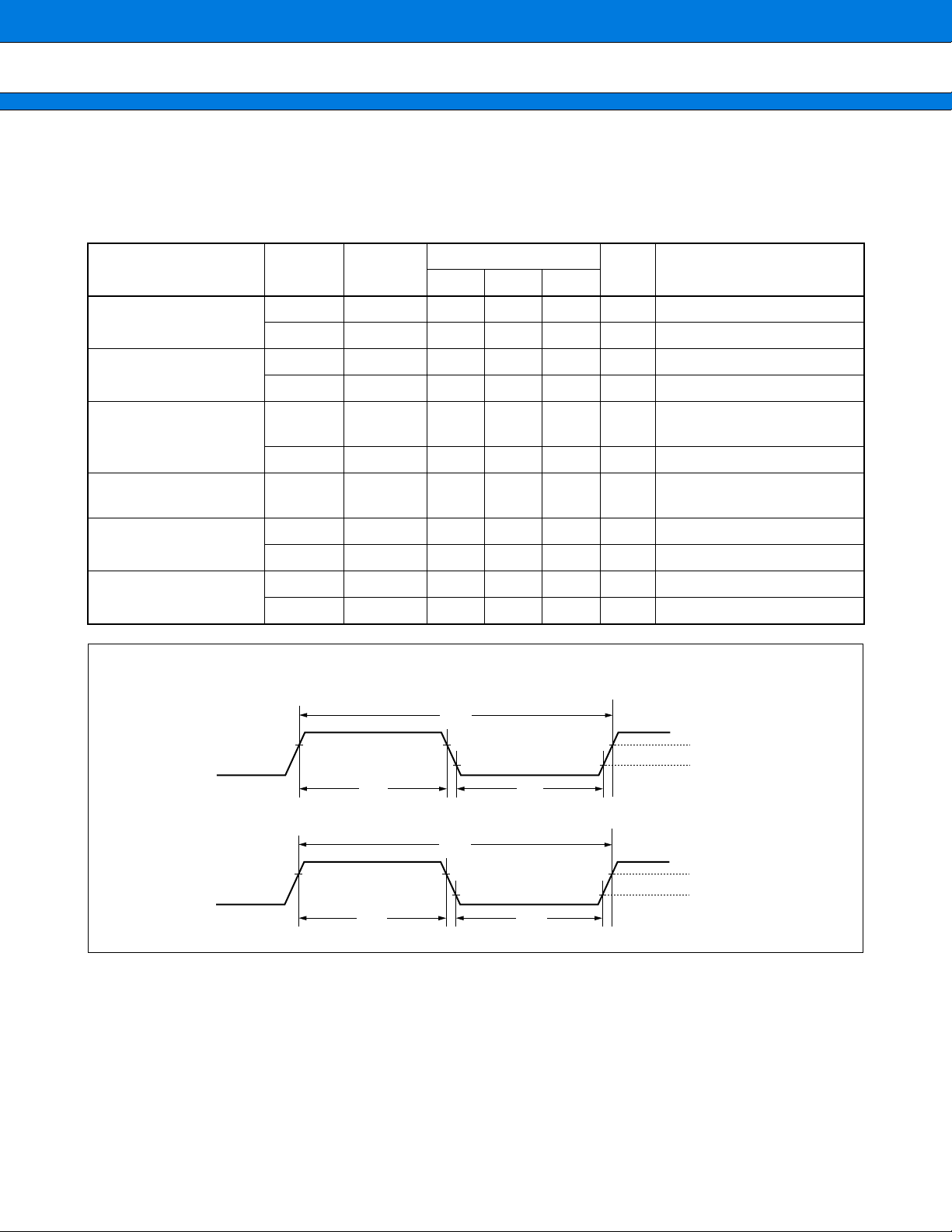
MB90495G Series
4. AC Characteristics
(1) Clock Timing
Parameter Symbol Pi n Name
C X0, X1 3 16 MHz
Clock frequency
Clock Cycle Time
f
f
CL X0A, X1A 32.768 kHz
tHCYL X0, X1 62.5 333 ns
t
LCYL X0A, X1A 30.5 µs
(V
CC = 5.0 V ± 5%, VSS = AVSS = 0.0 V, TA = −40 °C to +125 °C)
(V
CC = 5.0 V ± 10%, VSS = AVSS = 0.0 V, TA = −40 °C to +105 °C)
Value
Unit Remarks
Min Typ Max
Input clock pulse width
Input clock rising/falling
time
Internal operation clock
frequency
Internal operation clock
cycle time
• X0/X1 Clock Timing
X0
WH, PWL X0 10 ns
P
Duty ratio should be around
30 % to 70 %
PWLH, PWLL X0A 15.2 µs
t
CR, tCF X0 5 ns When external clock used
CP 1.5 16 MHz When oscillation circuit used
f
fLCP 8.192 kHz When subclock used
CP 62.5 666 ns When using oscillation circuit
t
t
LCP 122.1 µs When subclock used
tHCYL
0.8 VCC
0.2 VCC
PWH PWL
tCF tCR
tLCYL
68
X0A
0.8 VCC
0.2 VCC
PWLH PWLL
tCF tCR
Page 69

• PLL guaranteed operation range
Relationship between internal operating clock frequency and power supply voltage
5.5
5.25
4.75
4.5
3.3
3.0
Power supply voltage VCC (V)
MB90495G Series
MB90F497G/MB90F498G/MB90497G guaranteed operation range (T
MB90F497G/MB90F498G/MB90497G guaranteed operation range
( = +105°C <TA ≤+125°C)
PLL guaranteed operation range
81.5 3 12 16
Internal clock fCP (MHz)
A = −40
°
C to +105°C)
Relationship between external clock frequency and internal operation clock frequency
16
12
9
8
4
Internal clock fCP (MHz)
×4 ×3 ×2 ×1
34 8
External clock fC (MHz)
AC characteristics are specified by the following reference voltage values.
• Input Signal Waveform
Hysteresis Input Pin
0.8 VCC
0.2 VCC
• Output Signal Waveform
Output Pin
2.4 V
0.8 V
×1/2
(no multiplication)
16
69
Page 70

MB90495G Series
(2) Clock Output Timing
Parameter Symbol Pin Name Condition
Cycle time t
CLK ↑ → CLK ↓ t
CYC
CHCL 20 ns
CHCL
t
(V
CC = 5.0 V ± 5%, VSS = AVSS = 0.0 V, TA = −40 °C to +125 °C)
(V
CC = 5.0 V ± 10%, VSS = AVSS = 0.0 V, TA = −40 °C to +105 °C)
CLK
tCYC
Value
Unit Remarks
Min Max
62.5 ns
CLK
2.4 V 2.4 V
0.8 V
(3) Reset Input Timing
Parameter Symbol
Pin
Name
Condition
Value
Unit Remarks
Min Max
CP ns Normal mode
16 t
Stop mode,
Reset input time t
RSTL RST
Oscillator oscillation time*
CP
+ 16 t
ms
Watch mode,
Subclock mode,
Subsleep mode
* : Oscillator oscillation time is the time to reach 90% amplitude. For a crystal oscillator, this is a few to several
dozen ms; for a F AR/ceramic oscillator, this is se veral hundred µs to a few ms, and f or an external clock this is 0 ms.
• Stop mode, Watch mode, Subclock mode, Subsleep mode
tRSTL
RST
0.2 VCC 0.2 VCC
70
X0
Internal operation
clock
Internal reset
90% of
amplitude
Oscillator
oscillation time
16 tCP
Oscillation stabilize standby time
Instruction execution
Page 71

(4) Power-on Reset
Parameter Symbol
Pin
Name
MB90495G Series
(V
CC = 5.0 V ± 5%, VSS = AVSS = 0.0 V, TA = −40 °C to +125 °C)
(V
CC = 5.0 V ± 10%, VSS = AVSS = 0.0 V, TA = −40 °C to +105 °C)
Condition
Value
Unit Remarks
Min Max
Power supply rising time t
Power supply cutoff time t
VCC
Sudden changes in the power supply voltage may cause a power-on reset. To change the power
supply voltage while the device is in operation, it is recommended that you raise the voltage at a
steady rate, in order to suppress fluctuations (see figure below). In this case, perform this operation
when the PLL clock is not being used. If, however, the voltage falling speed is no more than 1 V/s,
it is permissible to perform this operation while using the PLL clock.
VCC
3 V
VSS
R VCC
0.05 30 ms
OFF VCC 1 ms Due to repeated operations
tR
2.7 V
0.2 V 0.2 V0.2 V
tOFF
It is recommended that you keep the rising
RAM data hold period
speed to no more than 50 mV/ms.
71
Page 72

MB90495G Series
(5) Bus Read Timing
Parameter Symbol Pin Name
(V
CC = 5.0 V±10%, VSS = 0.0 V, TA = −40 °C to +105 °C)
Value
Unit Remarks
Min Max
ALE pulse width t
Valid address → ALE ↓ time t
ALE ↓ → address valid time tLLAX
Valid address → RD
↓ time tAVRL
Valid address → Valid data input t
LHLL ALE tCP/2 − 20 ns
AVLL
AVDV
ALE, A23 to A16,
AD15 to AD00
ALE, AD15 to
AD00
A23 to A16,
AD15 to AD00, RD
A23 to A16,
AD15 to AD00
tCP/2 − 20 ns
tCP/2 − 15 ns
tCP − 15 ns
5 tCP/2 − 60 ns
RD pulse width tRLRH RD 3 tCP/2 − 20 ns
RD
↓ → valid data input tRLDV RD, AD15 to AD00 3 tCP/2 − 60 ns
RD
↑ → data hold time tRHDX RD, AD15 to AD00 0 ns
RD ↓ → ALE ↑ time tRHLH RD, ALE tCP/2 − 15 ns
RD
↑ → address valid time tRHAX RD, A23 to A16 tCP/2 − 10 ns
A23 to A16,
Valid address → CLK ↑ time t
AVCH
AD15 to AD00,
t
CP/2 − 20 ns
CLK
RD
↓ → CLK ↑ time tRLCH RD, CLK tCP/2 − 20 ns
ALE ↓ → RD ↓ time tLLRL ALE, RD tCP/2 − 15 ns
72
Page 73

• Bus read timing
MB90495G Series
CLK
ALE
RD
A23 to A16
AD15 to AD00
2.4 V
0.8 V
2.4 V
tAVCH
2.4 V
tAVLL tLLAX
tLHLL
tAVRL
2.4 V
0.8 V
Address
2.4 V
0.8 V
tAVDV
tLLRL
2.4 V
0.8 V
tRLCH
2.4 V
0.8 V
tRLDV
0.8 VCC
0.2 VCC
tRLRH
2.4 V
Read data
tRHLH
tRHAX
tRHDX
2.4 V
2.4 V
0.8 V
0.8 VCC
0.2 V
CC
73
Page 74

MB90495G Series
(6) Bus Write Timing
Parameter Symbol Pin Name
(V
CC = 5.0 V±10%, VSS = 0.0 V, TA = −40 °C to +105 °C)
Value
Unit Remarks
Min Max
Valid Address → WR
WR
pulse width tWLWH WR 3 tCP/2 − 20 ns
↓ time tAVWL
A23 to A16,
AD15 to AD00, WR
tCP − 15 ns
Valid data output → WR ↑ time tDVWH AD15 to AD00, WR 3 tCP/2 − 20 ns
WR
↑ → data hold time tWHDX AD15 to AD00, WR 20 ns
WR
↑ → address valid time tWHAX A23 to A16, WR tCP/2 − 10 ns
WR ↑ → ALE ↑ time tWHLH WR, ALE tCP/2 − 15 ns
WR
↑ → CLK ↑ time tWLCH WR, CLK tCP/2 − 20 ns
tWLCH
CLK
ALE
tAVWL tWLWH
2.4 V
tWHLH
2.4 V
74
WR (WRL, WRH)
A23 to A16
AD15 to AD00
2.4 V
0.8 V
0.8 V
2.4 V
0.8 V
2.4 V
Address Write data
0.8 V
tDVWH
2.4 V
tWHAX
2.4 V
0.8 V
tWHDX
2.4 V
0.8 V
Page 75

(7) Ready Input Timing
Parameter Symbol Pin Name
MB90495G Series
(V
CC = 5.0 V±10%, VSS = 0.0 V, TA = −40 °C to +105 °C)
Value
Min Max
Unit Remarks
RDY setup time t
RDY hold time t
RYHS RDY 45 ns
RYHH RDY 0 ns
Note : Use the automatic ready function if the setup time for the falling edge of the RDY signal is not sufficient.
• Ready Input timing
CLK
ALE
RD/WR
RDY
Unweighted
RDY
Weighted
(1 cycle)
0.8 V
0.2 VCC
2.4 V
tRYHS tRYHH
CC
0.8 VCC
(8) Hold Timing
(V
CC = 5.0 V±10%, VSS = 0.0 V, TA = −40 °C to +105 °C)
Value
Parameter Symbol Pin Name
Unit Remarks
Min Max
Pin in floating status → HAK
HAK
↑ → pin valid time tHAHV HAK tCP 2 tCP ns
↓ time tXHAL HAK 30 tCP ns
Note : It will take at least 1 cycle from the time the HRQ pin is loaded until the HAK changes.
• Hold Timing
HAK
Each pin
tXHAL
2.4 V
0.8 V
0.8 V
High-Z
2.4 V
tHAHV
2.4 V
0.8 V
75
Page 76

MB90495G Series
(9) UART Timing
Parameter Symbol Pin Name Condition
(V
CC = 5.0 V±5%, VSS = 0.0 V, TA = −40 °C to +125 °C)
(V
CC = 5.0 V±10%, VSS = 0.0 V, TA = −40 °C to +105 °C)
Value
Unit Remarks
Min Max
Serial clock cycle time t
SCK ↓ → SOT delay time t
SCYC SCK1
SLOV SCK1, SOT1 −80 80 ns
Internal shift clock
8 t
CP* ns
mode output pin :
Valid SIN → SCK ↑ tIVSH SCK1, SIN1 100 ns
SCK ↑ → valid SIN hold time t
Serial clock “H” pulse width t
SHIX SCK1, SIN1 60 ns
SHSL SCK1
Serial clock “L” pulse width tSLSH SCK1 4 tCP ns
SCK ↓ → SOT delay time t
Valid SIN → SCK ↑ t
SLOV SCK1, SOT1 150 ns
IVSH SCK1, SIN1 60 ns
C
L = 80 pF + 1 TTL
Eternal shift clock
mode outputpin :
C
L = 80 pF + 1 TTL
CP ns
4 t
SCK ↑ → valid SIN hold time tSHIX SCK1, SIN1 60 ns
* : See “ (1) Clock Timing” for details about t
CP (internal operating clock cycle time) .
Notes : • AC ratings are for CLK synchronous mode.
• C
L is the load capacitor value connected to pins while testing.
76
Page 77
• Internal shift clock mode
SCK
SOT
SIN
• External shift clock mode
SCK
MB90495G Series
tSCYC
2.4 V
0.8 V 0.8 V
tSLOV
2.4 V
0.8 V
tIVSH tSHIX
0.8 V
CC
0.2 VCC
tSLSH tSHSL
0.8 VCC 0.8 VCC
0.2 VCC 0.2 VCC
0.8 VCC
0.2 VCC
SOT
SIN
tSLOV
2.4 V
0.8 V
tIVSH tSHIX
0.8 V
CC
0.2 VCC
0.8 VCC
0.2 VCC
77
Page 78

MB90495G Series
(10) Timer Input Timing
Parameter Symbol Pin Name Condition
TIWH TIN0, TIN1, FRCK
Input pulse width
• Timer Input Timing
t
t
TIWL IN0 to IN3, FRCK
(V
CC = 5.0 V±5%, VSS = 0.0 V, TA = −40 °C to +125 °C)
(V
CC = 5.0 V±10%, VSS = 0.0 V, TA = −40 °C to +105 °C)
Value
Unit Remarks
Min Max
4 t
CP ns
TIN0, TIN1,
IN0 to IN3,
FRCK
(11) Timer Output Timing
Parameter Symbol Pin Name Condition
CLK ↑ → T
OUT change time tTO
• Timer Output Timing
CLK
TOT0, TOT1,
PPG0 to PPG3
0.8 VCC 0.8 VCC
tTIWH tTIWL
(V
(V
TOT0, TOT1,
PPG0 to PPG3
2.4 V
2.4 V
0.8 V
t
TO
0.2 VCC 0.2 VCC
CC = 5.0 V±5%, VSS = 0.0 V, TA = −40 °C to +125 °C)
CC = 5.0 V±10%, VSS = 0.0 V, TA = −40 °C to +105 °C)
Value
Unit Remarks
Min Max
30 ns
(12) Trigger Input Timing
Parameter Symbol Pin Name Condition
Input pulse width
• Trigger Input Timing
INT0 to INT7,
ADTG
78
t
TRGH
tTRGL
INT0 to INT7,
ADTG
0.8 VCC 0.8 VCC
tTRGH tTRGL
(V
CC = 5.0 V±5%, VSS = 0.0 V, TA = −40 °C to +125 °C)
(V
CC = 5.0 V±10%, VSS = 0.0 V, TA = −40 °C to +105 °C)
Value
Unit Remarks
Min Max
CP ns
5 t
Normal mode
1 µs
0.2 VCC 0.2 VCC
Stop mode
Page 79
MB90495G Series
5. A/D Converter
(VCC = AVCC = 5.0 V±5%, VSS = AVSS = 0.0 V, 3.0 V ≤ AVR − AVSS, TA = −40 °C to +125 °C)
(V
CC = AVCC = 5.0 V±10%, VSS = AVSS = 0.0 V, 3.0 V ≤ AVR − AVSS, TA = −40 °C to +105 °C)
Parameter Symbol Pin Name
Min Typ Max
Resolution 10 bit
Total error ±5.0 LSB
Nonlinearity error ±2.5 LSB
Differential linearity error ±1.9 LSB
Value
Unit Remarks
Zero transition voltage V
Full-scale transition voltage V
OT AN0 to AN7
FST AN0 to AN7
AVSS −
3.5 LSB
AVR −
6.5 LSB
AVSS +
0.5 LSB
AVR −
1.5 LSB
Conversion time 66 tCP ns
Sampling period 32 tCP ns
Analog port input current I
AIN AN0 to AN7 10 µA
AVSS +
4.5 LSB
AVR +
1.5 LSB
V
1 LSB =
AVR / 1024
V
Machine clock
of 16 MHz
Analog input voltage VAIN AN0 to AN7 AVSS AVR V
Reference voltage AVR AV
A AVCC 27mA
I
SS + 3.0 AVCC V
Power supply current
IAH AVCC 5 µA*
I
Reference voltage supply
current
R AVR 0.9 1.3 mA
I
RH AVR 5 µA*
Inter-channel variation AN0 to AN7 4LSB
* : Current (V
CC = AVCC = AVR = 5.0 V) when A/D converter is not operating and CPU is halted.
79
Page 80

MB90495G Series
6. A/D Converter Glossary
Resolution : Analog changes that are identifiable with the A/D converter
Linearity error : The deviation of the straight line connecting the zero transition point
( “00 0000 0000” ←→ “00 0000 0001” ) with the full-scale transition point
( “11 1111 1110” ←→ “11 1111 1111” ) from actual conversion characteristics.
Differential linearity error : The deviation of input voltage needed to change the output code b y 1 LSB from the
ideal value.
Total error : The difference between the actual value and the theoretical value, which includes
zero-transition error/full-scale transition error, linearity error, and differential linearity error.
Total error
3FF
3FE
3FD
004
Digital output
003
002
001
Total error of digital output N =
1 LSB = (ideal value)
Actual conversion
characteristics
Ideal characteristics
0.5 LSB
AV
SS AVR
Analog input
NT − {1 LSB × (N − 1) + 0.5 LSB}
V
AVR − AV
SS
1024
VOT (ideal value) = AVSS + 0.5 LSB [V]
V
FST (ideal value) = AVR − 1.5 LSB [V]
1.5 LSB
{1 LSB × (N − 1) + 0.5 LSB}
NT
V
(actual measurement)
Actual conversion
characteristics
1 LSB
[V]
[LSB]
80
V
NT : The voltage to transition digital output from N − 1 to N.
(Continued)
Page 81

(Continued)
3FF
3FE
3FD
004
Digital output
003
002
001
MB90495G Series
Linearity error
Actual conversion
characteristics
{1 LSB × (N − 1)
+ VOT }
Actual conversion
characteristics
Ideal characteristics
VOT (actual measurement)
AV
SS AVR AVSS AVR
FST
V
(actual
measurement)
NT
V
(actual
measurement)
N + 1
N
Digital output
N − 1
N − 2
Differential linearity error
Ideal
characteristics
Actual conversion
characteristics
VNT (actual measurement)
Actual conversion
characteristics
Analog inputAnalog input
(N + 1) T
V
(actual
measurement)
Linearity error of digital output N =
Differential linearity error of digital output N =
1 LSB =
V
OT : Voltage for transition from digital output 000H to 001H.
V
FST : Voltage for transition from digital output 3FEH to 3FFH.
NT − {1 LSB × (N − 1) + VOT}
1 LSB
V (
N + 1) T − VNT
1 LSB
VFST − VOT
1022
− 1 LSB [LSB]
[V]
[LSB]
V
7. Notes on Using A/D Converter
Select the output impedance value for the e x ternal circuit of analog input according to the following conditions :
External circuit output impedance values of about 5 kΩ or lower are recommended.
If external capacitors are used, a capacitance of several thousand times the internal capacitor value is recom-
mended in order to minimize the effect of voltage distribution between the external and internal capacitor.
If the output impedance of the external circuit is too high, the sampling time for analog voltages may not be
sufficient (sampling period = 2.00 µs @ machine clock of 16 MHz) .
• Model Analog Input Circuit
Comparator
Analog input
R
C
MB90F497G, MB90F498G, MB90V495G R 3.2 kΩ, C 30 pF
MB90497G R 2.6 kΩ, C 28 pF
Note : The figures given here are the suggested values.
•
About Error
The smaller the absolute value of | AVR - AV
SS |, the greater the relative error.
81
Page 82

MB90495G Series
8. Flash Memory Program/Erase Characteristics
Parameter Condition
Sector erase time
T
Chip erare time 5 s
A = + 25 °C
V
CC = 5.0 V
Min Typ Max
115s
Value
Unit Remarks
Excludes 00H programming prior
erasure
Excludes 00H programming prior
erasure
Word (16-bit width)
programming time
Erase/Program cycle 10,000 cycle
16 3,600 µs Excludes system-level overhead
82
Page 83

EXAMPLE CHARACTERISTICS
■
• MB90F497G/F498G
45
MB90495G Series
ICC − VCC
TA = 25 °C, external clock operation
f = internal operation frequency
40
35
30
25
20
ICC (mA)
15
10
5
0
3.0 4.0 5.0
TA = 25 °C, external clock operation
16
f = 16 MHz
f = 10 MHz
f = 8 MHz
f = 4 MHz
f = 2 MHz
6.0 7.0
V
CC (V)
I
CCS − VCC
f = internal operation frequency
14
12
10
8
ICCS (mA)
6
4
2
0
3.0 4.0 5.0
V
CC (V)
f = 16 MHz
f = 10 MHz
f = 8 MHz
f = 4 MHz
f = 2 MHz
6.0 7.0
(Continued)
83
Page 84

MB90495G Series
(Continued)
180
160
140
ICCL − VCC
TA = 25 °C, external clock operation
f
= internal operation frequency
120
100
80
ICCL (µA)
60
40
20
0
3.0 4.0 5.0
TA = 25 °C, external clock operation
10
9
8
7
6
5
ICCLS (µA)
4
3
2
1
0
3.0 4.0 5.0
f = 8 kHz
6.0 7.0
V
CC (V)
CCLS − VCC
I
f = internal operation frequency
f = 8 kHz
6.0 7.0
V
CC (V)
84
(Continued)
Page 85

(Continued)
MB90495G Series
ICCT − VCC
TA = 25 °C, external clock operation
f = internal operation frequency
7
1000
900
800
6
5
4
3
ICCT (µA)
2
1
0
3.0 4.0 5.0
(V
CC − VOH) − IOH
TA = 25 °C, VCC = 4.5 V
V
CC (V)
1000
900
800
f = 8 kHz
6.0 7.0
OL − IOL
V
TA = 25 °C, VCC = 4.5 V
700
600
500
VCC - VOH (mV)
400
300
200
100
0
0123456
7 8 9 10 11 12
IOH (mA)
700
600
500
VOL (V)
400
300
200
100
0
0123456
7 8 9 10 11 12
I
OL (mA)
85
Page 86

MB90495G Series
• MB90497G
45
40
ICC − VCC
TA = 25 °C, external clock operation
f = internal operation frequency
35
30
25
20
ICC (mA)
15
10
5
0
3.0 4.0 5.0
TA = 25 °C, external clock operation
16
14
12
6.0 7.0
V
CC (V)
I
CCS − VCC
f
= internal operation frequency
f = 16 MHz
f = 10 MHz
f = 8 MHz
f = 4 MHz
f = 2 MHz
f = 16 MHz
86
10
8
ICCS (mA)
6
4
2
0
3.0 4.0 5.0
V
CC (V)
f = 10 MHz
f = 8 MHz
f = 4 MHz
f = 2 MHz
6.0 7.0
(Continued)
Page 87

(Continued)
25
MB90495G Series
ICCL − VCC
TA = 25 °C, external clock operation
f
= internal operation frequency
20
15
ICCL (µA)
10
5
0
3.0 4.0 5.0
TA = 25 °C, external clock operation
10
9
8
7
6
5
ICCLS (µA)
4
3
2
1
0
3.0 4.0 5.0
f = 8 kHz
6.0 7.0
V
CC (V)
CCLS − VCC
I
f
= internal operation frequency
f = 8 kHz
6.0 7.0
V
CC (V)
(Continued)
87
Page 88

MB90495G Series
(Continued)
7
6
5
4
3
ICCT (µA)
2
1
0
3.0 4.0 5.0
ICCT − VCC
TA = 25 °C, external clock operation
f = internal operation frequency
6.0 7.0
V
CC (V)
f = 8 kHz
TA = 25 °C, VCC = 4.5 V
1000
900
800
700
600
500
VCC - VOH (mV)
400
300
200
100
0
0123456
(V
CC − VOH) − IOH
IOH (mA)
7 8 9 10 11 12
TA = 25 °C, VCC = 4.5 V
1000
900
800
700
600
500
VOL (V)
400
300
200
100
0
0123456
OL − IOL
V
I
OL (mA)
7 8 9 10 11 12
88
Page 89

ORDERING INFORMATION
■
Part Number Package Remarks
MB90F497GPF
MB90497GPF
MB90F498GPF
MB90F497GPFM
MB90497GPFM
MB90F498GPFM
MB90495G Series
64-pin plastic QFP
(FPT-64P-M06)
64-pin plastic LQFP
(FPT-64P-M09)
89
Page 90

MB90495G Series
PACKAGE DIMENSIONS
■
64-pin plastic QFP
(FPT-64P-M06)
52
64
119
24.70±0.40(.972±.016)
*
20.00±0.20(.787±.008)
INDEX
1.00(.039)
0.42±0.08
(.017±.003)
Note 1) * : These dimensions do not include resin protrusion.
Note 2) Pins width and pins thickness include plating thickness.
Note 3) Pins width do not include tie bar cutting remainder.
0.17±0.06
18.70±0.40
(.736±.016)
(.007±.002)
Details of "A" part
+0.35
–0.20
3.00
.118
0~8˚
1.20±0.20
(.047±.008)
(Mounting height)
+.014
–.008
+0.15
–0.20
0.25
+.006
–.008
.010
(Stand off)
3351
32
*
14.00±0.20
(.551±.008)
20
0.20(.008)
M
"A"
C
2003 FUJITSU LIMITED F64013S-c-5-5
0.10(.004)
0.10(.004)
Dimensions in mm (inches)
Note : The values in parentheses are reference values.
(Continued)
90
Page 91
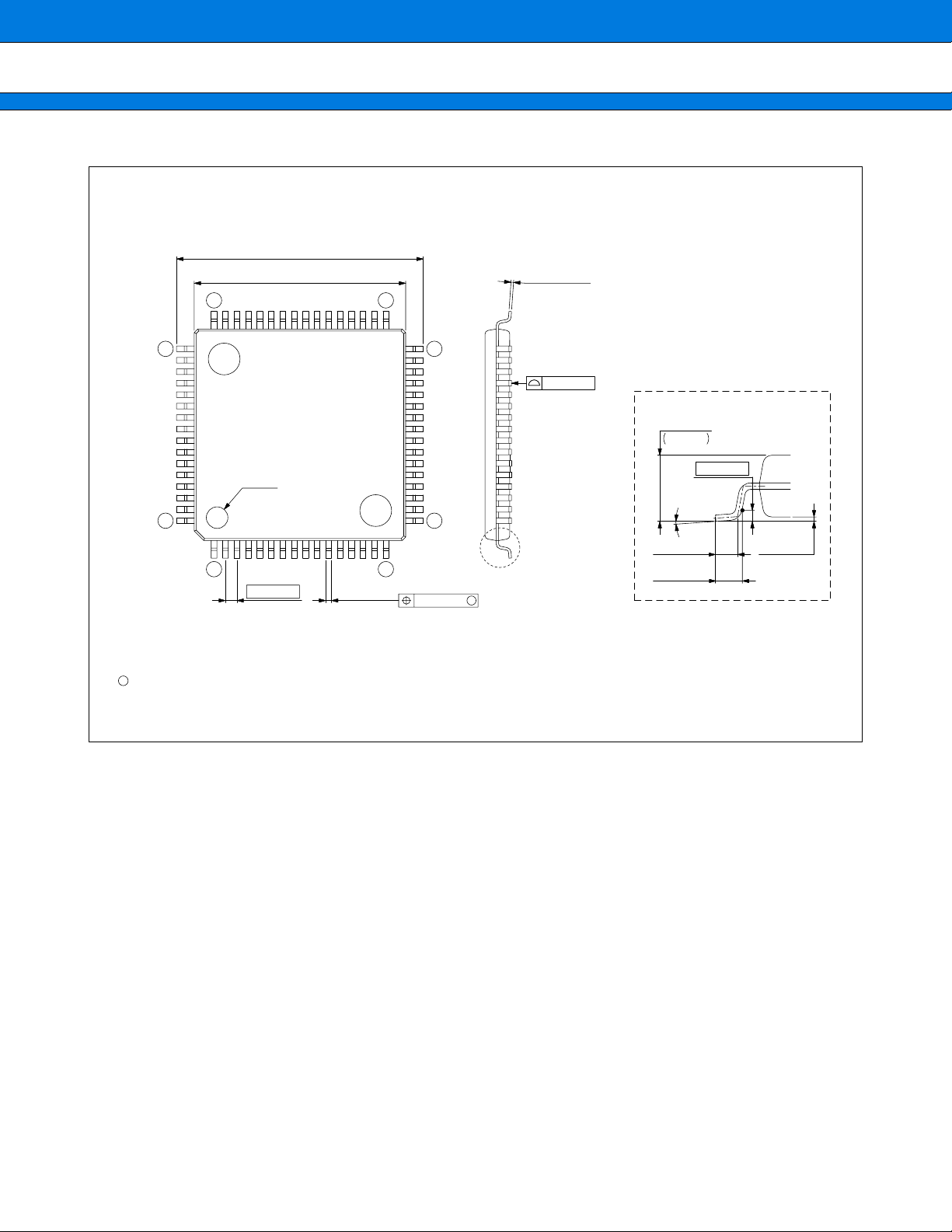
(Continued)
64-pin plastic LQFP
(FPT-64P-M09)
14.00±0.20(.551±.008)SQ
12.00±0.10(.472±.004)SQ
*
MB90495G Series
Note 1) * : These dimensions do not include resin protrusion.
Note 2) Pins width and pins thickness include plating thickness.
Note 3) Pins width do not include tie bar cutting remainder.
0.145±0.055
3348
(.0057±.0022)
49
INDEX
64
116
0.65(.026)
C
2003 FUJITSU LIMITED F64018S-c-3-5
0.32±0.05
(.013±.002)
32
0.10(.004)
0.10(.004)
Details of "A" part
+0.20
–0.10
1.50
(Mounting height)
+.008
–.004
.059
0.25(.010)
0~8˚
17
0.50±0.20
(.020±.008)
0.60±0.15
(.024±.006)
0.13(.005)
"A"
M
Dimensions in mm (inches)
Note : The values in parentheses are reference values.
0.10±0.10
(.004±.004)
(Stand off)
91
Page 92

MB90495G Series
FUJITSU LIMITED
All Rights Reserved.
The contents of this document are subject to change without notice.
Customers are advised to consult with FUJITSU sales
representatives before ordering.
The information, such as descriptions of function and application
circuit examples, in this document are presented solely for the
purpose of reference to show examples of operations and uses of
Fujitsu semiconductor device; Fujitsu does not warrant proper
operation of the device with respect to use based on such
information. When you develop equipment incorporating the
device based on such information, you must assume any
responsibility arising out of such use of the information. Fujitsu
assumes no liability for any damages whatsoever arising out of
the use of the information.
Any information in this document, including descriptions of
function and schematic diagrams, shall not be construed as license
of the use or exercise of any intellectual property right, such as
patent right or copyright, or any other right of Fujitsu or any third
party or does Fujitsu warrant non-infringement of any third-party’s
intellectual property right or other right by using such information.
Fujitsu assumes no liability for any infringement of the intellectual
property rights or other rights of third parties which would result
from the use of information contained herein.
The products described in this document are designed, developed
and manufactured as contemplated for general use, including
without limitation, ordinary industrial use, general office use,
personal use, and household use, but are not designed, developed
and manufactured as contemplated (1) for use accompanying fatal
risks or dangers that, unless extremely high safety is secured, could
have a serious effect to the public, and could lead directly to death,
personal injury, severe physical damage or other loss (i.e., nuclear
reaction control in nuclear facility, aircraft flight control, air traffic
control, mass transport control, medical life support system, missile
launch control in weapon system), or (2) for use requiring
extremely high reliability (i.e., submersible repeater and artificial
satellite).
Please note that Fujitsu will not be liable against you and/or any
third party for any claims or damages arising in connection with
above-mentioned uses of the products.
Any semiconductor devices have an inherent chance of failure. You
must protect against injury, damage or loss from such failures by
incorporating safety design measures into your facility and
equipment such as redundancy, fire protection, and prevention of
over-current levels and other abnormal operating conditions.
If any products described in this document represent goods or
technologies subject to certain restrictions on export under the
Foreign Exchange and Foreign Trade Law of Japan, the prior
authorization by Japanese government will be required for export
of those products from Japan.
F0306
FUJITSU LIMITED Printed in Japan
 Loading...