

Page 1

FUJITSU SEMICONDUCTOR
DATA SHEET
ASSP For Power Supply Applications
(General Purpose DC/DC Converter)
1-ch DC/DC Converter IC
for low voltage
MB39A105
DESCRIPTION
■■■■
The MB39A105 is 1-channel DC/DC converter IC using pulse width modulation (PWM). This IC is ideal for up
conversion.
The minimum operating voltage is lo w (1.8 V) , and the MB39A105 is best for built-in power supply such as LCD
monitors. Also the short-circuit protection detection output function prevents input/output short on a chopper type
up-converter .
This product is covered by US Patent Number 6,147,477.
DS04-27233-2E
FEATURES
■■■■
• Power supply voltage range : 1.8 V to 6 V
• Reference voltage accuracy : ± 1 %
• High-frequency operation capability : 1 MHz (Max)
• Built-in standby function: 0 µA (Typ)
• Built-in timer-latch short-circuit protection circuit
• Built-in short-circuit protection detection output function
• Built-in soft-start circuit independent of loads
• Built-in totem-pole type output for Nch MOS FET
• Package : TSSOP-8P (Thickness 1.1 mm Max)
PACKAGE
■■■■
8-pin plastic TSSOP
(FPT-8P-M05)
Page 2

MB39A105
PIN ASSIGNMENT
■■■■
(TOP VIEW)
−INE
CSCP
VCC
SCPOD
1
2
3
4
(FPT-8P-M05)
8
7
6
5
FB
RT
GND
OUT
2
Page 3

MB39A105
PIN DESCRIPTION
■■■■
Pin No. Symbol I/O Descriptions
1 −INE I Error amplifiers (Error Amp) inverted input terminal
2CSCP Timer-latch short-circuit protection capacitor connection terminal
3VCC Power supply terminal
Open drain output terminal for short-circuit protection detection
4SCPODO
5 OUT O External Nch FET gate drive terminal
6GND Ground terminal
7RT Triangular wave oscillation frequency setting resistor connection terminal
8 FB O Error Amplifier (Error Amp) output terminal
During timer-latch short-circuit protection operation : Output “High-Z”
During normal operation : Output “L”
3
Page 4
MB39A105
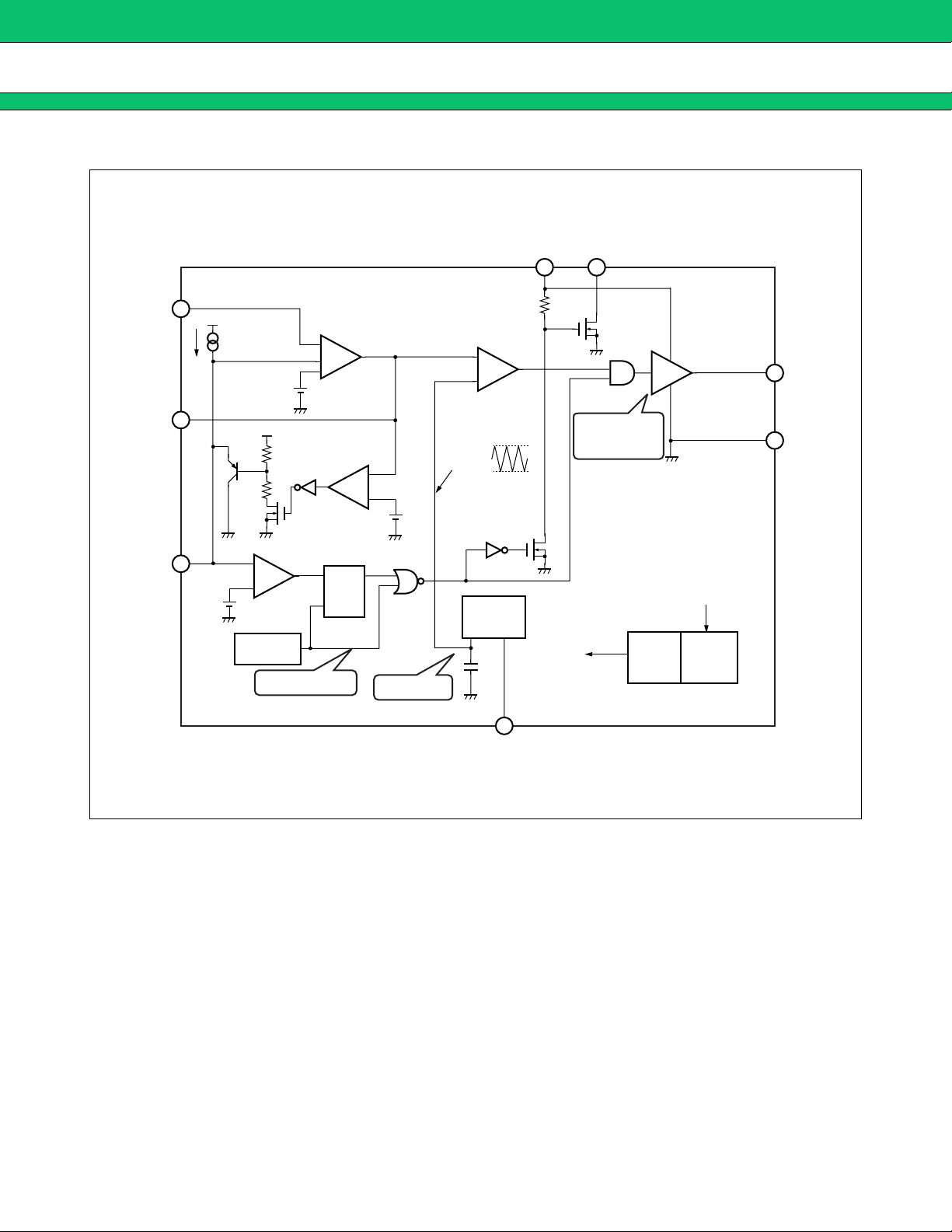
BLOCK DIAGRAM
■■■■
1
−INE
FB
VREF
8
VREF
Error Amp
−
+
+
(0.5 V ± 1%)
SCP
Comp.
+
−
(0.9 V)
+
−
(0.7 V)
(0.3 V)
PWM
Comp.
SCPODVCC
43
I
O = 400 mA
at VCC = 3.3 V
Nch
Drive
OUT
65GND
CSCP
2
(1.0 V)
+
−
UVLO
L : UVLO release
SQ
R
±10%
OSC
RT
RT Current
bias
VREF
(1.27 V)
7
VREF
Power
ON/OFF
CTL
4
Page 5

ABSOLUTE MAXIMUM RATINGS
■■■■
MB39A105
Parameter Symbol Condition
Unit
Min Max
Rating
Power supply voltage V
Output current I
Output peak current I
Power dissipation P
Storage temperature T
CC VCC terminal 7V
O OUT terminal 35 mA
OP Duty ≤ 5% (t = 1/fOSC×Duty) 700 mA
D Ta ≤ +25 °C 490* mW
STG −55 +125 °C
* : The packages are mounted on the epoxy board (10 cm × 10 cm).
WARNING: Semiconductor devices can be permanently damaged by application of stress (voltage, current,
temperature, etc.) in excess of absolute maximum ratings. Do not exceed these ratings.
RECOMMENDED OPERATING CONDITIONS
■■■■
Parameter Symbol Condition
Power supply voltage V
Input voltage V
SCPOD terminal output voltage V
SCPOD terminal output current I
Output current I
Min Typ Max
CC VCC terminal 1.8 6V
INE −INE terminal 0 VCC − 0.9 V
SCPOD SCPOD terminal 0 6V
SCPOT SCPOD terminal 0 2mA
O OUT terminal −30 +30 mA
Value
Unit
Oscillation frequency fosc 100 500 1000 kHz
Timing resistor R
Short-circuit detection capacitor C
T RT terminal 3.3 7.5 33 kΩ
SCP CSCP terminal 0.22 1.0 µF
Operating ambient temperature Ta −30 +25 +85 °C
WARNING: The recommended operating conditions are required in order to ensure the normal operation of the
semiconductor device. All of the device’s electrical characteristics are warranted when the device is
operated within these ranges.
Always use semiconductor devices within their recommended operating condition ranges. Operation
outside these ranges may adversely affect reliability and could result in device failure.
No warranty is made with respect to uses, operating conditions, or combinations not represented on
the data sheet. Users considering application outside the listed conditions are advised to contact their
FUJITSU representatives beforehand.
5
Page 6
MB39A105
ELECTRICAL CHARACTERISTICS
■■■■
Parameter
1. Under voltage
lockout
protection circuit
block [UVLO]
2. Short-circuit
protection block
[SCP]
3. Triangular
wave oscillator
[OSC]
block
4. Soft-start block
[CS]
5. Error amplifier
block [Error Amp]
6. PWM comparator block
[PWM Comp.]
7.Output block
[Drive]
8. General block
Threshold voltage V
Threshold voltage V
Short-circuit detection time
setting difference voltage
Input source current I
Reset voltage VRST 3VCC = 1.1 1.3 1.5 V
SCPOD terminal output
leak current
SCPOD terminal output on
resistor
Oscillation frequency fosc 5 RT = 7.5 kΩ 450 500 550 kHz
Frequency temperature
variation
Charge current I
Threshold voltage V
Input bias current IB 1 −INE = 0 V −120 −30 nA
Voltage gain AV 8DC 70* dB
Frequency band width BW 8 A
Output voltage
Output source current I
Output sink current ISINK 8FB = 0.5 V 100 300 µA
Maximum duty cycle Dtr 5 RT = 7.5 kΩ 85 90 95 %
Output source current I
Output sink current I
Output ON resistor
Standby current ICCS 3RT = OPEN 010µA
Power supply current I
(VCC = 3.3 V, Ta = +25 °C)
Symbol
∆V
CSCP 2CSCP = 0.85 V −1.76 −0.88 −0.44 µA
I
LEAK 4SCPOD = 3.3 V 01.0µA
R
∆f
f
OSC
Pin
No
TLH 3VCC = 1.15 1.35 1.55 V
TH 2 0.95 1.00 1.05 V
CSCP 2 0.15 0.20 0.25 V
ON 4SCPOD = 1 mA 50 100 Ω
OSC/
CS 2CSCP = 0 V −16 −11 −6 µA
TH 1FB = 0.5 V 0.495 0.5 0.505 V
5Ta = 0 °C to +85 °C 1* %
Conditions
V = 0 dB 1.1* MHz
Min Typ Max
Value
VOH 8 1.17 1.27 1.37 V
VOL 8 40 200 mV
SOURCE 8FB = 0.5 V −80 −50 µA
OUT = 0 V,
SOURCE 5
Duty ≤ 5%
−400* mA
(t = 1/fosc×Duty)
OUT = 3.3 V,
SINK 5
Duty ≤ 5%
400* mA
(t = 1/fosc×Duty)
R
OH 5OUT = −15 mA 4.0* Ω
ROL 5OUT = 15 mA 3.0 6.0 Ω
CC 3RT = 7.5 kΩ1.2 1.8 mA
Unit
*: Standard design value.
6
Page 7
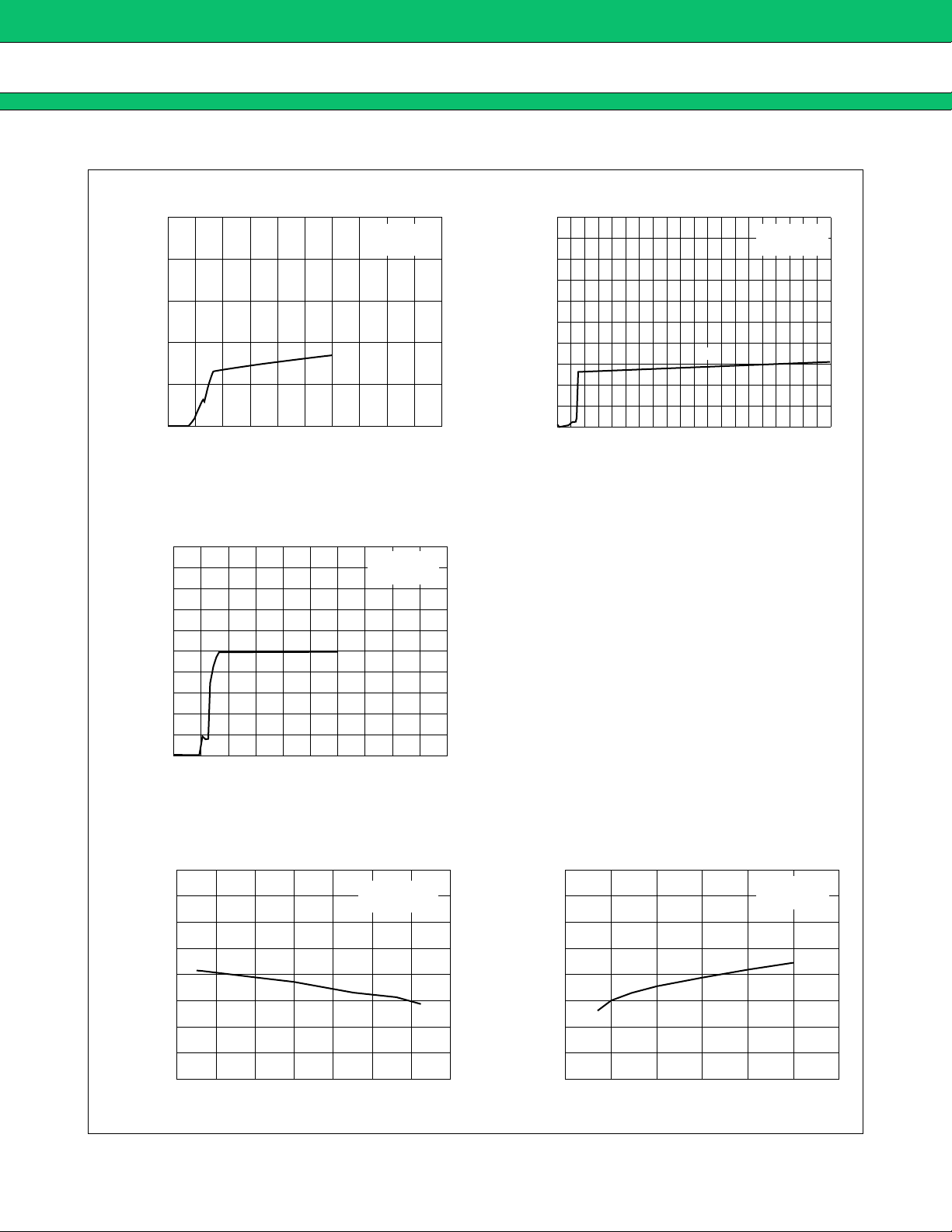
TYPICAL CHARACTERISTICS
■■■■
MB39A105
Power Supply Current vs. Power Supply Voltage
5
4
3
2
1
0
Power supply current ICC (mA)
0246810
Power supply voltage V
Ta = +25 °C
RT = 7.5 kΩ
CC (V)
Error Amplifier Threshold Voltage vs.
Power Supply Voltage
1.0
0.9
0.8
0.7
0.6
VTH (V)
0.5
0.4
0.3
Voltage
0.2
0.1
Error Amplifier Threshold
0.0
0246810
Ta = +25 °C
VCC = 3.3 V
Power supply voltage VCC (V)
Power Supply Current vs. RT Terminal Current
5.0
4.5
4.0
CC (mA)
3.5
3.0
2.5
2.0
1.5
1.0
0.5
Power supply current I
0.0
0 1020304050
I
CC
Ta = +25 °C
VCC = 3.3 V
RT terminal current IRT (µA)
Error Amplifier Threshold Voltage vs.
Ambient Temperature
0.52
0.51
VTH (V)
0.50
0.49
Voltage
Error Amplifier Threshold
0.48
−40 −20 0 20 40 60 80 100
Ambient temperature Ta (°C)
VCC = 3.3 V
RT = 7.5 kΩ
Triangular Wave Oscillation Frequency vs.
Power supply voltage
600
550
fOSC (kHz)
500
450
Frequency
Triangular Wave Oscillation
400
1234567
Power supply voltage V
Ta = +25 °C
RT = 7.5 kΩ
CC (V)
(Continued)
7
Page 8
MB39A105
Triangular Wave Oscillation Frequency
vs. Timing Resistor
10000
1000
OSC (kHz)
100
frequency f
Triangular wave oscillation
10
1 10 100
Timing resistor RT (kΩ)
Max On Duty vs.
Triangular Wave Oscillation Frequency
100
95
Ta = +25 °C
VCC = 3.3 V
Ta = +25 °C
VCC = 3.3 V
Triangular Wave Oscillation Frequency
vs. Ambient Temperature
600
550
OSC (kHz)
500
450
frequency f
Triangular wave oscillation
400
−40 −20 0 20 40 60 80 100
Ambient temperature Ta (°C)
VCC = 3.3 V
RT = 7.5 kΩ
90
85
80
Max On Duty (%)
75
70
10 100 1000 10000
Triangular wave oscillation frequency f
Error Amplifier Gain and Phase
vs. Frequency
40
30
20
10
V (dB)
−10
−20
Gain A
−30
−40
ϕ
0
Ta = +25 °C
VCC = 3.3 V
AV
OSC (kHz)
180
90
0
−90
Phase φ (deg)
−180
IN
10 kΩ
1 µF
+
10 kΩ
2.4 kΩ
10
11
240 kΩ
−
+
+
1.24 V
9
OUT
Error Amp
100 1 k 10 k 100 k 1 M 10 M
Frequency f (Hz)
(Continued)
8
Page 9

(Continued)
Power Dissipation vs. Ambient Temperature
600
500
490
400
300
200
100
Power dissipation PD (mW)
0
−40 −20 0 20 40 60 80 100
Ambient temperature Ta ( °C)
MB39A105
9
Page 10

MB39A105
FUNCTIONS
■■■■
1. DC/DC Converter Functions
(1) Triangular-wave oscillator block (OSC)
The triangular wave oscillator incorporates a timing resistor connected to RT terminal (pin 7) to generate
triangular oscillation waveform amplitude of 0.3 V to 0.7 V.
The triangular waveforms are input to the PWM comparator in the IC.
(2) Error amplifier block (Error Amp1, Error Amp2)
The error amplifier detects the DC/DC converter output voltage and outputs PWM control signals. In addition,
an arbitrary loop gain can be set by connecting a feedback resistor and capacitor from the output terminal to
inverted input terminal of the error amplifier, enabling stable phase compensation to the system.
Also, it is possib le to prevent rush current at power supply start-up by connecting a soft-start capacitor with the
CSCP terminal (pin 2) which is the non-inverted input terminal for Error Amp. The use of Error Amp for soft-start
detection makes it possible for a system to operate on a fixed soft-start time that is independent of the output
load on the DC/DC converter.
(3) PWM comparator block (PWM Comp.)
The PWM comparator is a voltage-to-pulse width modulator that controls the output duty depending on the input/
output voltage.
The comparator keeps output transistor on while the error amplifier output v oltage and the DTC voltage remain
higher than the triangular wave voltage.
(4) Output block (Drive)
The output block is in the totem pole configuration, capable of driving an external N-channel MOS FET.
10
Page 11

MB39A105
2. Power Control Function
A switch in series with a resistor connected with the RT terminal (pin 7) allows y ou to turn on or turn off the pow er.
On/off setting conditions of power supply
CTL Power
L OFF (standby)
H ON (operating)
ON/OFF CTL
(L : OFF, H : ON)
RT
3. Protective Functions
(1) Timer-latch short-circuit protection circuit (SCP)
Short-circuit detection comparator detects the error amplifier output voltage level. If the load conditions for the
DC/DC converter are stable, the short-circuit protection comparator is kept in equilibrium condition because the
error amplifier is free from output variation. At this time the CSCP terminal (pin 2) is held at the soft-start end
voltage (about 0.8 V) . If the DC/DC conver ter output voltage falls and error amplifier output is over 0.9 V, the
timer circuits are actuated to start charging the external capacitor C
When the capacitor voltage reaches about 1.0 V, the latch is set and the circuit is turned off the external FET
and sets the dead time to 100 %. At this time, latch input is closed and the CSCP terminal is held at the “L” level.
To reset the actuated protection circuit, turn off and on the power supply again and set VCC terminal voltage
(pin 3) to 1.1 V (Min) or less. (See ■SETTING TIME CONSTANT FOR TIMER-LATCH SHORT-CIRCUIT PR OTECTION CIRCUIT.)
(2) Under voltage lockout protection circuit (UVLO)
SCP.
The transient state or a momentary decrease in supply voltage, which occurs when the power supply is turned
on, may cause the IC to malfunction, resulting in breakdown or degradation of the system. To prevent such
malfunctions, under voltage loc kout protection circuit detects a decrease in internal reference voltage with respect
to the power supply voltage, turns off the output FET, and sets the dead time to 100% while holding the CSCP
terminal (pin 2) at the “L” level.
The circuit restores the output transistor to normal when the supply voltage reaches the threshold voltage of the
undervoltage lockout protection circuit.
(3) Short-circuit protection detection output function
Connecting the Pch MOS FET to SCPOD terminal (pin 4) turns off the Pch MOS FET when the shor t-circuit
protection is detected or under voltage lockout protection circuit operate. This allows you to prevent the shortcircuit between the input and output when the short-circuit protection is detected, thus preventing the input
voltage from occurring in the output region in the standby state.
(4) Protection circuit operating function table
This table refers to output condition when protection circuit is operating.
Operating circuit SCPOD OUT
Short-circuit protection circuit High-Z L
Under voltage lockout protection circuit High-Z L
11
Page 12

MB39A105
SETTING THE OUTPUT VOLTAGE
■■■■
• Output Voltage Setting Circuit
VO
R1
1
R2
SETTING THE TRIANGULAR OSCILLATION FREQUENCY
■■■■
−INE
CSCP
2
−
+
+
(0.5 V)
Error
Amp
V
O (V) = (R1 + R2)
0.5
R2
The triangular oscillation frequency is determined by the timing resistor (RT) connected to the RT terminal (pin 7) .
Triangular oscillation frequency : fosc
fosc (kHz) :=
3750
T (kΩ)
R
12
Page 13

MB39A105
SETTING THE SOFT-START TIMES
■■■■
To prevent r ush currents when the IC is tur ned on, you can set a soft-star t by connecting soft-star t capacitors
(C
SCP) to the CSCP terminal (pin 2). When IC star ts (VCC ≥ UVLO threshold voltage), the exter nal soft-start
capacitors (C
determined by comparison between the lower one of the potentials at two non-inverted input terminals (0.5 V
in an internal reference voltage, CSCP terminal voltages) and the inverted input terminal voltage (−INE (pin 1)
voltage).
The FB terminal voltage is decided for the soft-start period by the comparison between 0.5 V in an internal
reference voltage and the v oltages of the CSCP terminal. The DC/DC converter output voltage rises in proportion
to the CSCP terminal voltage as the soft-start capacitor connected to the CSCP terminal is charged.
The soft-start time is obtained from the following formula:
Soft-start time: ts (time to output 100%)
ts (s) := 0.045 × C
SCP) connected to CSCP terminal are charged at 11 µA. The error amplifier output (FB (pin 8) ) is
SCP (µF)
• Soft-Start Circuit
R1
R2
:= 0.8 V
:= 0.5 V
:= 0 V
VO
Soft-start time (ts)
−INE
1
CSCP
2
CSCP terminal voltage
Error Amp block −INE voltage
t
VREF
11 µA
L priority
Error Amp
−
+
+
(0.5 V)
C
SCP
FB
8
UVLO
13
Page 14

MB39A105
SETTING TIME CONST ANT FOR TIMER-LA TCH SHORT -CIRCUIT PRO TECTION CIRCUIT
■■■■
The error amplifier’s output level alaways does the comparison operation with the short-circuit protection comparator (SCP Comp.) to the reference voltage.
While DC/DC converter load conditions are stable, the short-circuit detection comparator output remains stable,
and the CSCP terminal (pin 2) is held at soft-start end voltage (about 0.8 V) .
If the load condition changes rapidly due to a short-circuit of the load and the DC/DC converter output voltage
drops, the output of the error amplifier usually goes over 0.9 V. In that case, the capacitor C
When the capacitor C
SCP is charged to about 1.0 V, the latch is set and the external FET is turned off (dead time
is set to 100%). At this time, the latch input is closed and the CSCP terminal (pin 2) is held at “L” level. When
CSCP terminal becomes “L” level, SCPOD terminal Nch MOS FET becomes OFF. SCPOD terminal (pin 4) is
held at “L” level and can be used as a short-circuit operating detection signal during normal operation.
To reset the actuated protection circuit, the power supply turn off and on again to lower the VCC terminal (pin
3) voltage to 1.1 V (Min) or less.
Short-circuit detection time (t
t
CSCP (s) := 0.23 × CSCP (µF)
•
Timer-latch short-circuit protection circuit
CSCP)
SCP is charged further.
R1
R2
O
V
8
FB
−INE
CSCP
1
(0.88 µA)(10.1 µA)
2
−
+
(1.0 V)
−
−
+
(0.5 V)
VREF
Error
Amp
SCP
Comp.
−
+
VREF
(0.9 V)
to Drive
14
SR
Latch UVLO
Page 15

•
Soft-start and short-circuit protection circuit timing chart
1.0 V
0.9 V
0.8 V
CSCP voltage
MB39A105
FB voltage
0.7 V
Soft-start time
t
S
Output
short
OSC
amplifier
Output short
Short-circuit detection time
t
CSCP
0.3 V
t
15
Page 16

MB39A105
I/O EQUIVALENT CIRCUIT
■■■■
〈〈Soft-start block (CS) 〉〉 〈〈Short-circuit protection circuit block (SCP) 〉〉
3
VCC
ESD
protection
element
6
GND
ESD
protection
element
CSCP
2
ESD
protection
element
VCC
CSCP
GND
1.0 V
+
−
4
SCPOD
〈〈Triangular wave oscillator block (RT) 〉〉
VCC
0.33 V
GND
+
−
RT
7
〈〈Output block〉〉
VCC
OUT
5
GND
VCC
(1.27 V)
−INE
GND
〈〈Error amplifier block〉〉
1
CS
0.5 V
FB
8
16
Page 17

APPLICATION EXAMPLE
■■■■
Q1
R8
100 kΩ
SCPOD
4
L1
O
V
A
6.8 µH
(9.0 V)
D1
OUT
Drive
Q2
5
Nch
C7
C6
C5
C4
MB39A105
0.1 µF
4.7 µF
4.7 µF
4.7 µF
GND
6
CTL
Power
RT Current
ON/OFF
VREF
C3
C2
C1
O = 400 mA
4.7 µF
4.7 µF
0.1 µF
3
VCC
R6
R5
−INE
330 kΩ
43 kΩ
PWM
Error Amp
VREF
1
R7
A
Comp.
+
+
−
22 kΩ
R4
I
at VCC = 3.3 V
−
(0.7 V)
(0.3 V)
+
−
(0.9 V)
+
51 kΩ
(0.5 V ± 1%)
C9
8
0.1 µF
SCP
VREF
FB
Comp.
SQ
+
2
CSCP
−
(1.0 V)
C8
0.22 µF
R
bias
OSC
VREF
(1.27 V)
±10%
UVLO
L : UVLO release
RT
R1
7.5 kΩ
7
Q3
R11
100 kΩ
ON/OFF CTL
(L : OFF, H : ON)
VIN
(1.8 V to
6.0 V)
17
Page 18

MB39A105
PARTS LIST
■■■■
COMPONENT ITEM SPECIFICATION VENDOR PARTS No.
Q1 Pch FET VDS = 20 V, ID = −2 A (Max) SANYO MCH3306
Q2, Q3 Nch FET VDS = 20 V, Qg = 4.5 nC (Typ) SANYO MCH3405
D1 Diode VF = 0.40 V (Max) , at IF = 1 A SANYO SBS004
L1 Inductor 6.8 µH 1.4 A, 144 mΩ SUMIDA CMD5D13-6R8
C1, C7, C9
C2 to C6
C8
Ceramics Condenser
NeoCapacitor
Ceramics Condenser
0.1 µF
4.7 µF
0.22 µF
50 V
10 V
10 V
TDK
NEC/TOKIN
TDK
C1608JB1H104K
TEPSLA21A475M8R
C1608JB1A224K
R1
R4
R5
R6
R7
R8, R11
Note : SANYO : SANYO Electric Co., Ltd.
SUMIDA : SUMIDA Electric Co., Ltd.
TDK : TDK Corporation
NEC/TOKIN : NEC TOKIN Corporation
ssm : SUSUMU Co., Ltd.
Resistor
Resistor
Resistor
Resistor
Resistor
Resistor
7.5 kΩ
51 kΩ
43 kΩ
330 kΩ
22 kΩ
100 kΩ
0.5 %
0.5 %
0.5 %
0.5 %
0.5 %
0.5 %
ssm
ssm
ssm
ssm
ssm
ssm
RR0816P-752-D
RR0816P-513-D
RR0816P-433-D
RR0816P-334-D
RR0816P-223-D
RR0816P-104-D
18
Page 19

MB39A105
SELECTION OF COMPONENTS
■■■■
• Nch MOS FET
The N-ch MOSFET for switching use should be rated for at least 20% more than the maximum output voltage.
To minimize continuity loss, use a FET with low R
and high frequency operation, on/off-cycle switching loss will be higher so that power dissipation must be
considered. In this application, the SANYO MCH3405 is used. Continuity loss, on/off switching loss, and total
loss are determined by the following f ormulas. The selection must ensure that peak drain current does not exceed
rated values.
DS(ON) between the drain and source. For high output voltage
Continuity loss : P
C
PC = ID 2 × RDS(ON) × Duty
On-cycle switching loss : PS (ON)
P
S (ON) =
VD (Max) × ID × tr × fOSC
6
Off-cycle switching loss : PS (OFF)
P
S (OFF) =
VD (Max) × ID (Max) × tf × fOSC
6
Total loss : PT
PT = PC + PS (ON) + PS (OFF)
Example: Using the SANYO MCH3405
Input voltage V
f
OSC = 500 kHz, L = 6.8 µH, drain-source on resistance RDS (ON) := 160 mΩ, tr = 18 ns, tf = 8 ns.
Drain current (Max) : I
I
D (Max) =
=
IN (Max) = 2.4 V, output voltage VO = 9 V, drain current ID = 0.94 A, Oscillation frequency
D (Max)
VO × IO
VIN(Min) 2L VO
9 × 0.25
2.4 2 × 6.8 × 10
+
+
VIN(Min)
ton ton =
2.4× (9−2.4)
−6
×
× 9500 × 10
1
VO − VIN(Min)
3
t
:= 1.20 (A)
Drain current (Min) : ID (Min)
ID (Min) =
VO × IO
VIN(Min) 2L
9 × 0.25
=
2.4 2 × 6.8 × 10
−
−
:= 0.68 (A)
VIN(Min)
ton
2.4× (9−2.4)
−6
×
× 9 500 × 10
1
3
19
Page 20

MB39A105
C = ID
P
2
× RDS (ON) × Duty
= 0.94
2
× 0.16 ×
9−2.4
:= 0.104 W
PS (ON) =
PS (OFF) =
VD (Max) × ID × tr × fOSC
6
9 × 0.94 × 18 × 10
=
:= 0.013
W
VD (Max) × ID (Max) × tf × fOSC
6
9 × 1.20 × 8 × 10−9 × 500 × 10
=
:=
0.007 W
PT = PC + PS (ON) + PS (OFF)
:= 0.104 + 0.013 + 0.007
:= 0.
124 W
9
−9
6
6
× 500 × 10
3
3
The above power dissipation figures for the MCH3405 is satisfied with ample margin at 0.8 W.
• Inductors
In selecting inductors, it is of course essential not to apply more current than the rated capacity of the inductor ,
but also to note that the lower limit for ripple current is a cr itical point that if reached will cause discontinuous
operation and a considerable drop in efficiency. This can be prevented by choosing a higher inductance value,
which will enable continuous operation under light loads. Note that if the inductance value is too high, however,
direct current resistance (DCR) is increased and this will also reduce efficiency. The inductance must be set at
the point where efficiency is greatest.
Note also that the DC superimposition characteristics become worse as the load current value approaches the
rated current value of the inductor , so that the inductance v alue is reduced and ripple current increases, causing
loss of efficiency. The selection of rated current value and inductance value will var y depending on where the
point of peak efficiency lies with respect to load current.
Inductance values are determined by the following formulas.
Inductance value : L
2
L ≥
VIN
2IOVO
ton
20
Page 21

Example:
MB39A105
IN (Max)
2IOVO
4
2
ton
2
×
9−4
×
1
3
L ≥
V
≥
2 × 0.25 × 9 9 500 × 10
≥ 3.95 µH
Inductance values derived from the above formulas are values that provide sufficient margin for continuous
operation at maximum load current, but at which continuous oper ation is not possible at light loads. It is theref ore
necessary to determine the load level at which continuous operation becomes possible. In this application, the
Sumida CMD5D13-6R8 is used. At 6.8 µH, the load current value under continuous operating conditions is
determined by the following formula.
Load current value under continuous operating conditions : I
IO ≥
≥
VIN (Max)
2 × 6.8 × 10
2LVO
2
ton
2
4
−6
× 9 9 500 × 10
×
9−4
×
1
3
O
≥ 145.2 mA
To determine whether the current through the inductor is within rated values, it is necessary to determine the
peak value of the ripple current as well as the peak-to-peak values of the ripple current that affect the output
ripple voltage. The peak value and peak-to-peak value of the ripple current can be determined by the following
formulas.
Peak value : I
IL ≥
L
VO × IO
VIN 2L VO
VIN
+
ton ton =
VO − VIN
t
Peak-to-peak value : ∆IL
∆IL =
VIN
L
ton
Example: Using the CMD5D13-6R8
6.8 µH (allowable tolerance ±20%) , rated current = 1.4 A
Peak value:
I
L ≥
≥
VO × IO
VIN 2L VO
9 × 0.25
2.4 2 × 6.8 × 10
VIN
+
+
ton
ton =
2.4 × (9 − 2.4)
−6
× 9 500 × 10
VO − VIN
×
t
1
3
≥ 1.20 A
21
Page 22

MB39A105
Peak-to-peak value:
L =
∆I
• Flyback diode
The flyback diode is generally used as a Shottky barrier diode (SBD) when the reverse voltage to the diode is
less than 40V. The SBD has the characteristics of higher speed in terms of faster reverse recovery time, and
lower forw ard v oltage , and is ideal f or achieving high efficiency . As long as the DC re v erse voltage is sufficiently
higher than the output voltage, the average current flowing through the diode is within the mean output current
level, and peak current is within peak surge current limits, there is no problem. In this application the SANYO
SBS004 is used. The diode mean current and diode peak current can be calculated by the following formulas.
VIN (Min)
L
4 × (9 − 4)
=
6.8 × 10
:= 0.654 A
ton
−6
×
× 9 500 × 10
1
3
Diode mean current : I
IDi ≥ IO × (1 −
VO−VIN (Min)
VO
Di
)
Diode peak current : IDip
IDip ≥
VO × IO
VIN (Min) 2L
+
VIN (Min)
ton
Example: Using the SANYO SBS004
VR (DC reverse voltage) = 15 V, mean output current = 1.0 A, peak surge current = 10 A,
VF (forward voltage) = 0.40 V, IF = 1.0 A
I
Di ≥ IO × (1 −
VO−VIN (Min)
VO
)
≥ 0.25 × (1 − 0.733)
≥ 66.8 mA
IDip ≥
VO × IO
VIN (Min) 2L
+
VIN (Min)
ton
≥ 1.20 A
22
Page 23

MB39A105
• Smoothing Capacitor
The smoothing capacitor is an indispensable element for reducing ripple v oltage in output. In selecting a smoothing capacitor it is essential to consider equivalent series resistance (ESR) and allowable ripple current. Higher
ESR means higher ripple voltage, so that to reduce ripple voltage it is necessary to select a capacitor with low
ESR. However, the use of a capacitor with low ESR can have substantial effects on loop phase characteristics,
and therefore requires attention to system stability. Care should also be taken to use a capacity with sufficient
margin for allowable ripple current. This application uses the TEPSLA21A475M8R (NEC/TOKIN) . The ESR,
capacitance value, and ripple current can be calculated from the following formulas.
Equivalent Series Resistance : ESR
ESR ≤
∆VO
∆IL 2πfCL
−
1
Capacitance value : C
CL ≥
2πf (∆VO − ∆IL × ESR)
∆IL
L
Ripple current : ∆ICL
V
∆IC
L ≥
IN
ton
L
Example: Using the TEPSLA21A475M8R (Three piecies are parallel.)
Rated voltage = 10 V, ESR = 500 mΩ, maximum allowable ripple current = 1 A
Equivalent series resistance
ESR ≤
≤
O
∆V
∆IL 2πfCL
0.18
0.654 2π × 500 × 10
−
−
1
1
3
× 14.1 × 10
−6
≤ 252.7 mΩ
Capacitance value : C
CL ≥
2πf (∆VO − ∆IL × ESR)
≥
2π × 500 × 10
L
∆IL
0.39
3
× (0.18 − 0.654 × 0.167)
p−p
≥ 2.94
µF
Ripple current : ∆ICL
V
4 × (9 − 4)
≥
6.8 × 10
IN
ton
L
∆ICL ≥
≥ 0.654 Ap−p
−6
×
× 9 500 × 10
1
3
23
Page 24

MB39A105
REFERENCE DATA
■■■■
100
Ta = +25 °C
9 V output
90
80
70
60
Conversion efficiency η (%)
50
Conversion Efficiency vs. Load current
Vin = 1.8 V
Vin = 3.3 V
Vin = 6.0 V
40
30
1 m 10 m 100 m 1
Load current IL (A)
Switching Wave Form
VG (V)
V
D (V)
10
5
0
15
10
5
0
Ta = +25 °C
VIN = 3.3 V
O = 9 V
V
I
O = 100 mA
24
012345678910
t (µs)
Page 25

MB39A105
USAGE PRECAUTION
■■■■
•
Printed circuit board ground lines should be set up with consideration for common impedance.
•
Take appropriate static electricity measures.
• Containers for semiconductor materials should hav e anti-static protection or be made of conductive material.
• After mounting, printed circuit boards should be stored and shipped in conductive bags or containers.
• Work platforms, tools, and instruments should be properly grounded.
• Working personnel should be grounded with resistance of 250 kΩ to 1 MΩ between body and ground.
•
Do not apply negative voltages.
The use of negative voltages below –0.3 V may create parasitic transistors on LSI lines, which can cause
abnormal operation.
ORDERING INFORMATION
■■■■
Part number Package Remarks
MB39A105PFT
8-pin plastic TSSOP
(FPT-8P-M05)
25
Page 26

MB39A105
PACKAGE DIMENSION
■■■■
8-pin plastic TSSOP
(FPT-8P-M05)
3.00±0.10(.118±.004)
INDEX
5
4
(.009
4.40
±0.10 6.40±0.20
0.22±0.10
±.004)
0.10(.004)
8
1
0.65(.026)
1.95(.077)
C
2002 FUJITSU LIMITED F08013Sc-1-1
(.252
0.127±0.03
±.001)
(.0050
±.008)(.173±.004)
Details of "A" part
1.10(.043)MAX
"A"
0~8˚
0.54(.021) 0.10±0.10
(.004
±.004)
Dimensions in mm (inches)
26
Page 27

MB39A105
FUJITSU LIMITED
All Rights Reserved.
The contents of this document are subject to change without notice.
Customers are advised to consult with FUJITSU sales
representatives before ordering.
The information and circuit diagrams in this document are
presented as examples of semiconductor device applications, and
are not intended to be incorporated in devices for actual use. Also,
FUJITSU is unable to assume responsibility for infringement of
any patent rights or other rights of third parties arising from the use
of this information or circuit diagrams.
The products described in this document are designed, developed
and manufactured as contemplated for general use, including
without limitation, ordinary industrial use, general office use,
personal use, and household use, but are not designed, developed
and manufactured as contemplated (1) for use accompanying fatal
risks or dangers that, unless extremely high safety is secured, could
have a serious effect to the public, and could lead directly to death,
personal injury, severe physical damage or other loss (i.e., nuclear
reaction control in nuclear facility, aircraft flight control, air traffic
control, mass transport control, medical life support system, missile
launch control in weapon system), or (2) for use requiring
extremely high reliability (i.e., submersible repeater and artificial
satellite).
Please note that Fujitsu will not be liable against you and/or any
third party for any claims or damages arising in connection with
above-mentioned uses of the products.
Any semiconductor devices have an inherent chance of failure. You
must protect against injury, damage or loss from such failures by
incorporating safety design measures into your facility and
equipment such as redundancy, fire protection, and prevention of
over-current levels and other abnormal operating conditions.
If any products described in this document represent goods or
technologies subject to certain restrictions on export under the
Foreign Exchange and Foreign Trade Law of Japan, the prior
authorization by Japanese government will be required for export
of those products from Japan.
F0209
FUJITSU LIMITED Printed in Japan
 Loading...