

Page 1

FUJITSU MICROELECTRONICS
DATA SHEET
DS04-27231-5Ea
ASSP For Power Management Applications
(General Purpose DC/DC Converter)
2-ch DC/DC Converter IC
with Overcurrent Protection
MB39A104
■ DESCRIPTION
The MB39A104 is a 2-channel DC/DC converter IC using pulse width modulation (PWM), incorporating an
overcurrent protection circuit (requiring no current sense resistor). This IC is ideal for down conversion.
Operating at high frequency reduces the value of coil.
This is ideal for built-in power supply such as LCD monitors and ADSL.
This product is covered by US Patent Number 6,147,477.
■ FEATURES
• Built-in timer-latch overcurrent protection circuit (requiring no current sense resistor)
• Power supply voltage range : 7 V to 19 V
• Reference voltage : 5.0 V ± 1 %
• Error amplifier threshold voltage : 1.24 V ± 1 %
• High-frequency operation capability : 1.5 MHz (Max)
• Built-in standby function: 0 µA (Typ)
• Built-in soft-start circuit independent of loads
• Built-in totem-pole type output for P-ch MOS FET
• One type of package (SSOP-24 pin : 1 type)
■ APPLICATION
• LCD monitor/panel
• IP phone
• Printer
• Video capture etc.
Copyright©2002-2008 FUJITSU MICROELECTRONICS LIMITED All rights reserved
2006.8
Page 2

MB39A104
■ PIN ASSIGNMENTS
(TOP VIEW)
VCCO :
VH :
OUT1 :
VS1 :
ILIM1 :
DTC1 :
VCC :
CSCP :
FB1 :
−INE1 :
CS1 :
RT :
10
11
12
1
2
3
4
5
6
7
8
9
24
23
22
21
20
19
18
17
16
15
14
13
: CTL
: GNDO
: OUT2
: VS2
: ILIM2
: DTC2
: GND
: VREF
: FB2
: −INE2
: CS2
: CT
(FPT-24P-M03)
2
Page 3

MB39A104
■ PIN DESCRIPTION
Pin No. Symbol I/O Descriptions
1 VCCO ⎯ Output circuit power supply terminal (Connect to same potential as VCC pin)
2 VH O Power supply terminal for FET drive circuit (VH = V
3 OUT1 O External P-ch MOS FET gate drive terminal
4 VS1 I Overcurrent protection circuit input terminal
Overcurrent protection circuit detection resistor connection terminal. Set
5ILIM1I
6DTC1I
7VCC⎯
8CSCP⎯ Timer-latch short-circuit protection capacitor connection terminal
9 FB1 O Error amplifier (Error Amp 1) output terminal
10 −INE1 I Error amplifier (Error Amp 1) inverted input terminal
11 CS1 ⎯ Soft-start capacitor connection terminal
12 RT ⎯ Triangular wave oscillation frequency setting resistor connection terminal
13 CT ⎯ Triangular wave oscillation frequency setting capacitor connection terminal
14 CS2 ⎯ Soft-start capacitor connection terminal
15 −INE2 I Error amplifier (Error Amp 2) inverted input terminal
16 FB2 O Error amplifier (Error Amp 2) output terminal
overcurrent detection reference voltage depending on external resistor and
internal current resource (110 µA at R
PWM comparator block (PWM) input terminal. Compares the lowest voltage
among FB1 and DTC1 terminals with triangular wave and controls output.
Power supply terminal for reference power supply and control circuit
(Connect to same potential as the VCCO terminal)
T = 24 kΩ)
CC − 5 V)
17 VREF O Reference voltage output terminal
18 GND ⎯
19 DTC2 I
20 ILIM2 I
21 VS2 I Overcurrent protection circuit input terminal
22 OUT2 O External P-ch MOS FET gate drive terminal
23 GNDO ⎯ Output circuit ground terminal (Connect to same potential as GND terminal)
24 CTL I
Output circuit ground terminal (Connect to same potential as GNDO
terminal.)
PWM comparator block (PWM) input terminal. Compares the lowest voltage
among FB2 and DTC2 terminals with triangular wave and controls output.
Overcurrent protection circuit detection resistor connection terminal. Set
overcurrent detection reference voltage depending on external resistor and
internal current resource (110 µA at R
Power supply control terminal. Setting the CTL terminal at “L” level places IC
in the standby mode.
T = 24 kΩ)
3
Page 4
MB39A104
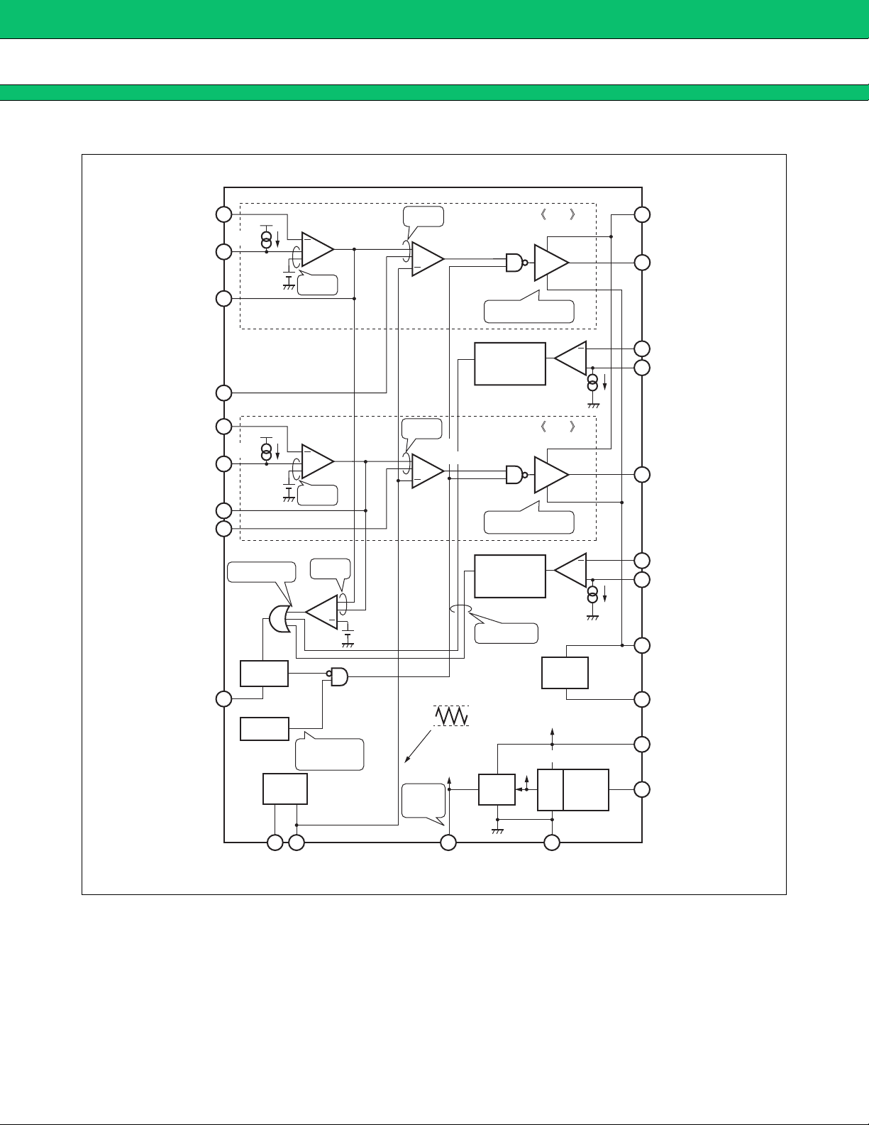
■ BLOCK DIAGRAM
−INE1
10
10 µA
11
CS1
9
FB1
6
DTC1
VREF
1.24 V
Error
Amp1
+
+
L priority
L priority
PWM
Comp.1
+
+
P-ch
IO = 200 mA
at VCCO = 12 V
Current
Protection
Logic
CH1
Drive1
1
VCCO
OUT1
3
VS1
4
+
5
ILIM1
−INE2
CS2
FB2
DTC2
CSCP
15
14
16
19
8
VREF
10 µA
1.24 V
H: at SCP
+
+
L priority
H priority
SCP
Comp.
Error
Amp2
+
+
(3.1 V)
SCP
Logic
UVLO
H:UVLO
release
OSC
12 13 1817
RT CT GNDVREF
L priority
PWM
Comp.2
+
+
2.5 V
1.5 V
Accuracy
±1%
5.0 V
bias
CH2
Drive2
P-ch
I
O = 200 mA
at VCCO = 12 V
Current
Protection
Logic
H: at OCP
VH
Bias
Voltage
Error Amp Power Supply
Error Amp Referennce
1.24 V
VREF
VR1
+
V
CC − 5 V
Powe r
ON/OFF
CTL
22
21
20
2
23
7
24
OUT2
VS2
ILIM2
VH
GNDO
VCC
CTL
4
Page 5
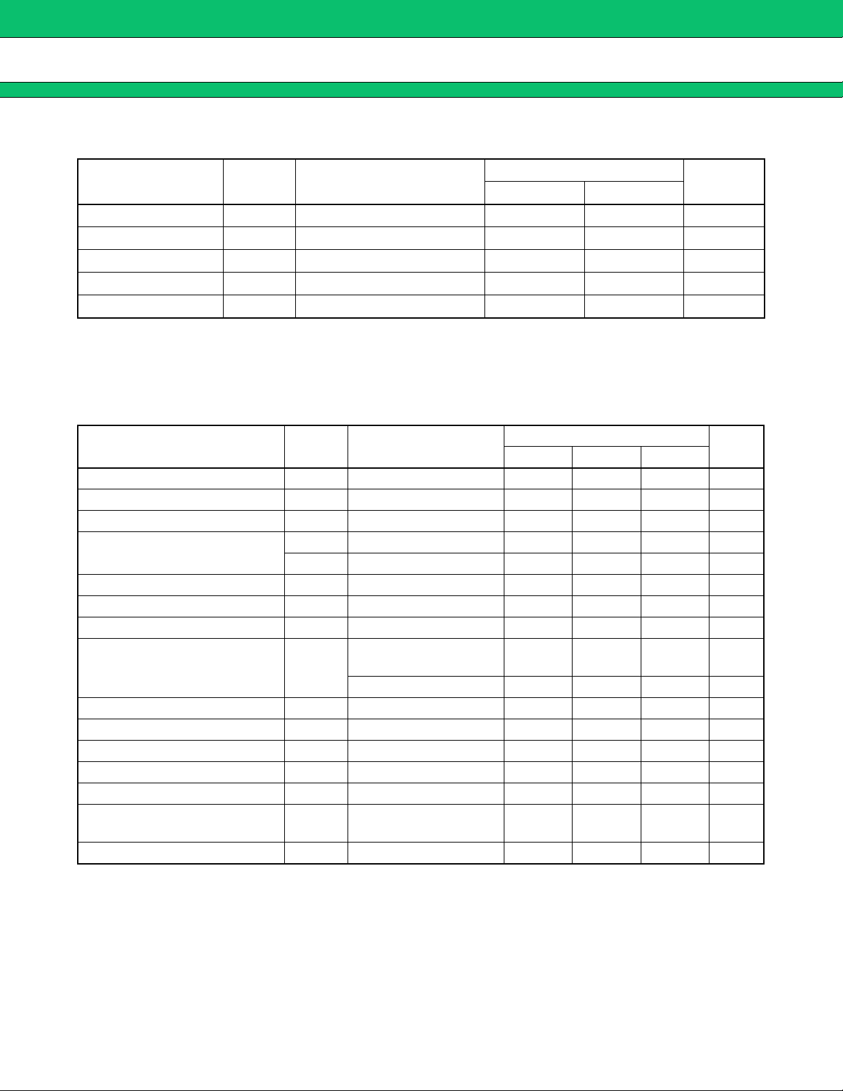
■ ABSOLUTE MAXIMUM RATINGS
MB39A104
Parameter Symbol Condition
Unit
Min Max
Rating
Power supply voltage V
Output current I
Output peak current I
Power dissipation P
Storage temperature T
CC VCC, VCCO terminal ⎯ 20 V
O OUT1, OUT2 terminal ⎯ 60 mA
OP Duty ≤ 5% (t = 1/fOSC×Duty) ⎯ 700 mA
D Ta ≤ +25 °C ⎯ 740* mW
STG ⎯−55 +125 °C
* : The packages are mounted on the epoxy board (10 cm × 10 cm).
WARNING: Semiconductor devices can be permanently damaged by application of stress (voltage, current,
temperature, etc.) in excess of absolute maximum ratings. Do not exceed these ratings.
■ RECOMMENDED OPERATING CONDITIONS
Parameter Symbol Condition
Power supply voltage V
Reference voltage output current I
VH output current I
Input voltage
V
Control input voltage V
Output current I
Output Peak current I
Oscillation frequency f
CC VCC, VCCO terminal 7 12 19 V
REF VREF terminal −1 ⎯ 0mA
VH VH terminal 0⎯30 mA
V
INE −INE1, −INE2 terminal 0 ⎯ VCC − 0.9 V
DTC DTC1, DTC2 terminal 0 ⎯ VCC − 0.9 V
CTL CTL terminal 0 ⎯ 19 V
O OUT1, OUT2 terminal −45 ⎯+45 mA
Duty ≤ 5% (t = 1/fOSC×Duty)
OP
Overcurrent detection
OSC
by ON resistance of FET
Min Typ Max
−450 ⎯+450 mA
100 500 1000 kHz
* 100 500 1500 kHz
Timing capacitor C
Timing resistor R
VH terminal capacitor C
Soft-start capacitor C
Short-circuit detection capacitor C
Reference voltage output
capacitor
T ⎯ 39 100 560 pF
T ⎯ 11 24 130 kΩ
VH VH terminal ⎯ 0.1 1.0 µF
S CS1, CS2 terminal ⎯ 0.1 1.0 µF
SCP CSCP terminal ⎯ 0.1 1.0 µF
C
REF VREF terminal ⎯ 0.1 1.0 µF
Operating ambient temperature Ta ⎯−30 +25 +85 °C
Val ue
Unit
* : Refer to“ ■ SETTING THE TRIANGULAR OSCILLATION FREQUENCY”.
WARNING: The recommended operating conditions are required in order to ensure the normal operation of the
semiconductor device. All of the device’s electrical characteristics are warranted when the device is
operated within these ranges.
Always use semiconductor devices within their recommended operating condition ranges. Operation
outside these ranges may adversely affect reliability and could result in device failure.
No warranty is made with respect to uses, operating conditions, or combinations not represented on
the data sheet. Users considering application outside the listed conditions are advised to contact their
representatives beforehand.
5
Page 6

MB39A104
■ ELECTRICAL CHARACTERISTICS
Parameter
Output voltage VREF 17 Ta = +25 °C 4.95 5.00 5.05 V
Output voltage
temperature
variation
Input stability Line 17 VCC = 7 V to 19 V ⎯ 310mV
voltage
Load stability Load 17 VREF = 0 mA to −1 mA ⎯ 110mV
block [REF]
1.Reference
Short-circuit
output current
Threshold
voltage
2.Under
voltage lockout
Hysteresis
block [UVLO]
width
protection circuit
Threshold
voltage
Input source
current
[SCP Logic]
3.Short-circuit
Reset voltage V
detection block
Symbol
∆V
REF/
V
REF
I
OS 17 VREF = 1 V −50 −25 −12 mA
V
TLH 17 VREF = 2.6 2.8 3.0 V
V
THL 17 VREF = 2.4 2.6 2.8 V
H 17 ⎯⎯0.2* ⎯ V
V
V
TH 8 ⎯ 0.68 0.73 0.78 V
I
CSCP 8 ⎯−1.4 −1.0 −0.6 µA
RST 17 VREF = 2.4 2.6 2.8 V
Pin No Conditions
(VCC = VCCO = 12 V, VREF = 0 mA, Ta = +25 °C)
Val ue
Unit
Min Typ Max
17 Ta = 0 °C to +85 °C ⎯ 0.5* ⎯%
Threshold
voltage
[SCP Comp.]
4.Short-circuit
detection block
Oscillation
frequency
[OSC]
Frequency
temperature
block
6.Soft-
5.Triangular
start
variation
wave oscillator
Charge current ICS 11, 14 CS1 = CS2 = 0 V −14 −10 −6 µA
block
[CS1, CS2]
Threshold
voltage
Input bias
block
7.Error amplifier
current
[Error Amp1,
Error Amp2]
Voltage gain A
V
TH 8 ⎯ 2.8 3.1 3.4 V
f
OSC 13 CT = 100 pF, RT = 24 kΩ 450 500 550 kHz
∆f
OSC/
f
OSC
V
TH 9, 16 FB1 = FB2 = 2 V 1.227 1.240 1.253 V
I
B 10, 15 −INE1 = −INE2 = 0 V −120 −30 ⎯ nA
V 9, 16 DC ⎯ 100* ⎯ dB
13 Ta = 0 °C to +85 °C ⎯ 1* ⎯%
(Continued)
6
Page 7

(Continued)
[Error Amp1,
Error Amp2]
7.Error amplifier block
block
(VCC = VCCO = 12 V, VREF = 0 mA, Ta = +25 °C)
Parameter Symbol Pin No. Conditions
Frequency
bandwidth
BW 9, 16 A
V
OH 9, 16 ⎯ 4.7 4.9 ⎯ V
V = 0 dB ⎯ 1.6* ⎯ MHz
Output voltage
V
OL 9, 16 ⎯⎯40 200 mV
Output source
current
Output sink current I
I
SOURCE 9, 16 FB1 = FB2 = 2 V ⎯−2 −1mA
SINK 9, 16 FB1 = FB2 = 2 V 150 200 ⎯µA
V
T0 6, 19 Duty cycle = 0 % 1.4 1.5 ⎯ V
Threshold voltage
T100 6, 19 Duty cycle = Dtr ⎯ 2.5 2.6 V
V
MB39A104
Val ue
Unit
Min Typ Max
PWM Comp.2]
[PWM Comp.1,
8.PWM comparator
block
9.Overcurrent
10.Bias
[OCP1, OCP2]
protection circuit
[VH]
block
voltage
[Drive1, Drive2]
11.Output block
[CTL]
12.Control block
Input current I
ILIM terminal input
current
Offset voltage V
Output voltage VH 2
Output source
current
DTC 6, 19 DTC1 = DTC2 = 0.4 V −2.0 −0.6 ⎯µA
I
LIM 5, 20 RT = 24 kΩ, CT = 100 pF 99 110 121 µA
IO 5, 20 ⎯⎯1* ⎯ mV
VCC = VCCO = 7 V to 19 V
VH = 0 mA to 30 mA
VCC−
5.5
VCC−
5.0
VCC−
4.5
OUT1 to OUT4 = 7 V,
ISOURCE 3, 22
Duty ≤ 5 %
(t = 1/f
OSC×Duty)
⎯−300 ⎯ mA
V
OUT1 to OUT4 = 12 V,
Output sink current I
Output ON
resistor
SINK 3, 22
OH 3, 22 OUT1 = OUT2 = −45 mA ⎯ 8.0 12.0 Ω
R
R
OL 3, 22 OUT1 = OUT2 = 45 mA ⎯ 6.5 9.7 Ω
IH 24 IC Active mode 2 ⎯ 19 V
V
Duty ≤ 5 %
(t = 1/f
OSC×Duty)
⎯ 350 ⎯ mA
CTL input voltage
V
IL 24 IC Standby mode 0 ⎯ 0.8 V
I
CTLH 24 CTL = 5 V ⎯ 50 100 µA
Input current
I
CTLL 24 CTL = 0 V ⎯⎯ 1 µA
Standby current ICCS 1, 17 CTL = 0 V ⎯ 010µA
Power supply
current
13.General
*: Standard design value.
I
CC 1, 17 CTL = 5 V ⎯ 4.0 6.0 mA
7
Page 8
MB39A104
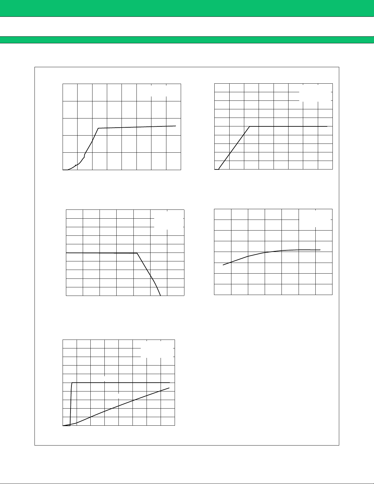
■ TYPICAL CHARACTERISTICS
Power Supply Current vs. Power Supply Voltage
10
8
6
4
2
Power supply current ICC (mA)
0
0 5 10 15 20
Power supply voltage VCC (V) Power supply voltage VCC (V)
Ta = +25 °C
CTL = 5 V
Reference Voltage vs. Load current
10
8
6
4
Ta = +25 °C
VCC = 12 V
CTL = 5 V
Reference Voltage vs. Power Supply Voltage
10
8
REF (V)
6
4
2
Reference voltage V
0
0 5 10 15 20
= +25 °C
Ta
CTL = 5 V
VREF = 0 mA
Reference Voltage vs. Ambient Temperature
2.0
1.5
1.0
0.5
0.0
−0.5
VCC
= 12 V
CTL = 5 V
VREF = 0 mA
2
Reference voltage VREF (V)
0
0 5 10 15 20 25 30 35
Load current IREF (mA)
CTL terminal Current vs. CTL terminal Voltage
500
400
300
200
100
CTL terminal current ICTL (µA)
0
0 5 10 15 20
VREF
ICTL
Ta = +25 °C
VCC = 12 V
VREF = 0 mA
CTL terminal voltage VCTL (V)
10
9
8
7
6
5
4
3
2
1
0
Reference voltage VREF (V)
−1.0
−1.5
Reference voltage ∆VREF (%)
−2.0
−40 −20 0 +20 +40 +60 +80 +100
Ambient temperature Ta (°C)
(Continued)
8
Page 9
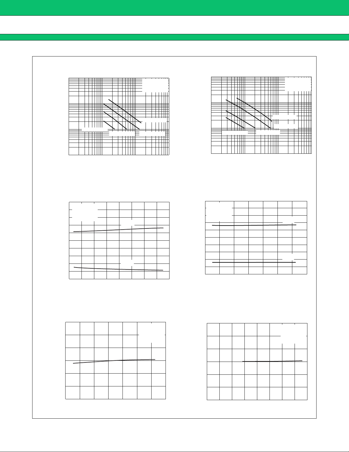
MB39A104
0
Triangular Wave Oscillation Frequency
vs. Timing Resistor
10000
OSC (kHz)
frequency f
Triangular wave oscillation
1000
100
10
CT = 560 pF
1 10 100 1000
CT = 220 pF
Timing resistor RT (kΩ)
Ta = +25 °C
VCC = 12 V
CTL = 5 V
CT = 39 pF
CT = 100 pF
Triangular Wave Upper and Lower Limit Voltage
vs. Triangular Wave Oscillation Frequency
3.2
3.0
2.8
CT (V)
2.6
2.4
2.2
2.0
1.8
1.6
1.4
lower limit voltage V
Triangular wave upper and
1.2
Triangular wave oscillation frequency fOSC (kHz)
= +25 °C
Ta
VCC = 12 V
CTL = 5 V
R
T = 47 kΩ
0 200 400 600 800 1000 1200
Upper
Lower
16001400
Triangular Wave Oscillation Frequency
vs. Timing Capacitor
Triangular wave oscillation
10000
OSC (kHz)
frequency f
1000
100
RT = 130 kΩ
10
10 100 1000 1000
RT = 68 kΩ
Timing capacitor CT (pF)
Ta = +25 °C
VCC = 12 V
CTL = 5 V
RT = 11 kΩ
RT = 24 kΩ
Triangular Wave Upper and Lower Limit Voltage
vs. Ambient Temperature
3.2
VCC = 12 V
3.0
CTL = 5 V
R
T = 24 kΩ
2.8
CT = 100 pF
CT (V)
2.6
2.4
2.2
2.0
1.8
1.6
1.4
lower limit voltage V
Triangular wave upper and
1.2
−40 −20 0 +20 +40 +60 +80 +100
Ambient temperature Ta ( °C)
Upper
Lower
Triangular Wave Oscillation Frequency
vs. Ambient Temperature
560
540
520
OSC (kHz)
500
480
frequency f
460
Triangular wave oscillation
440
−40 −20 0 +20 +40 +60 +80 +100
Ambient temperature Ta ( °C)
VCC = 12 V
CTL = 5 V
R
T = 24 kΩ
CT = 100 pF
Triangular Wave Oscillation Frequency
vs. Power supply voltage
560
540
520
OSC (kHz)
500
480
frequency f
460
Triangular wave oscillation
440
0 5 10 15 20
Power supply voltage VCC (V)
Ta = +25 °C
CTL = 5 V
R
T = 24 kΩ
CT = 100 pF
(Continued)
9
Page 10
MB39A104
(Continued)
Error Amplifier, Gain, Phase vs. Frequency
Ta = +25 °C
VCC = 12 V
A
V
Gain AV (dB)
40
30
20
10
0
−10
−20
−30
−40
100 1 k 10 k 100 k 1 M 10 M
ϕ
Frequency f (Hz)
Power Dissipation vs. Ambient Temperature
1000
800
740
180
90
0
−90
−180
240 kΩ
10 kΩ
1 µF
+
IN
2.4 kΩ
10 kΩ
Phase φ (deg)
(15)
10
11
(14)
−
+
+
1.24 V
9
(16)
Error Amp1
(Error Amp2)
OUT
600
400
200
Power dissipation PD (mW)
0
−40 −20 0 +20 +40 +60 +80 +100
Ambient temperature Ta ( °C)
10
Page 11

MB39A104
■ FUNCTIONS
1. DC/DC Converter Functions
(1) Reference voltage block (REF)
The reference voltage circuit generates a temperature-compensated reference voltage (5.0 V Typ) from the
voltage supplied from the VCC terminal (pin 7). The voltage is used as the reference voltage for the IC’s internal
circuitry.
The reference voltage can supply a load current of up to 1 mA to an external device through the VREF terminal
(pin 17).
(2) Triangular-wave oscillator block (OSC)
The triangular wave oscillator incorporates a timing capacitor and a timing resistor connected respectively to
the CT terminal (pin 13) and RT terminal (pin 12) to generate triangular oscillation waveform amplitude of 1.5 V
to 2.5 V.
The triangular waveforms are input to the PWM comparator in the IC.
(3) Error amplifier block (Error Amp1, Error Amp2)
The error amplifier detects the DC/DC converter output voltage and outputs PWM control signals. In addition,
an arbitrary loop gain can be set by connecting a feedback resistor and capacitor from the output terminal to
inverted input terminal of the error amplifier, enabling stable phase compensation to the system.
Also, it is possible to prevent rush current at power supply start-up by connecting a soft-start capacitor with the
CS1 terminal (pin 11) and CS2 terminal (pin 14) which are the non-inverted input terminal for Error Amp. The
use of Error Amp for soft-start detection makes it possible for a system to operate on a fixed soft-start time that
is independent of the output load on the DC/DC converter.
(4) PWM comparator block (PWM Comp.1, PWM Comp.2)
The PWM comparator is a voltage-to-pulse width modulator that controls the output duty depending on the input/
output voltage.
The comparator keeps output transistor on while the error amplifier output voltage remain higher than the
triangular wave voltage.
(5) Output block (Drive1, Drive2)
The output block is in the totem pole configuration, capable of driving an external P-channel MOS FET.
(6) Bias voltage block (VH)
This bias voltage circuit outputs V
circuit outputs the potential equal to V
CC − 5 V(Typ) as minimum potential of the output circuit. In standby mode, this
CC.
11
Page 12

MB39A104
2. Control Function
When CTL terminal (pin 24) is “L” level, IC becomes the standby mode. The power supply current is 10 µA (Max)
at the standby mode.
On/Off Setting Conditions
CTL Power
L OFF (Standby)
H ON (Operating)
3. Protective Functions
(1) Timer-latch overcurrent protection circuit block (OCP)
The timer-latch overcurrent protection circuit is actuated upon completion of the soft-start period. When an
overcurrent flows, the circuit detects the increase in the voltage between the FET’s drain and source using the
external FET ON resistor, actuates the timer circuit, and starts charging the capacitor C
CSCP terminal (pin 8). If the overcurrent remains flowing beyond the predetermined period of time, latch is set
and OUT terminals (pin 3,22) of each channel are fixed at “H” level. And the circuit sets the latch to turn off the
external FET. The detection current value can be set by resistor R
the ILIM1 terminal (pin 5) and resistor R
LIM2 connected between the drain and the ILIM2 terminal (pin 20).
LIM1 connected between the FET’s drain and
Changing connection enables to detect overcurrent at current sense resistor.
To reset the actuated protection circuit, either the power supply turn off and on again or set the CTL terminal
(pin 6) to the “L” level to lower the VREF terminal (pin 17) voltage to 2.4 V (Min) or less. (Refer to “1. Setting
Timer-Latch Overcurrent Protection Detection Current” in “■ABOUT TIMER-LATCH PROTECTION CIRCUIT”.)
SCP connected to the
(2) Timer-latch short-circuit protection circuit (SCP Logic, SCP Comp.)
The short-circuit detection comparator (SCP Comp.) detects the output voltage level of Error Amp, and if the
error amp output voltage of any channel falls below the short-circuit detection voltage (3.1 V Typ), the timer
circuits are actuated to start charging the external capacitor C
SCP connected to the CSCP terminal (pin 8).
When the capacitor voltage reaches about 0.73 V, the circuit is turned off the output transistor and sets the dead
time to 100 %.
To reset the actuated protection circuit, either the power supply turn off and on again or set the CTL terminal
(pin 24) to the “L” level to lower the VREF terminal (pin 17) voltage to 2.4 V (Min) or less. (Refer to “2. Setting
Time Constant for Timer-Latch Short-Circuit Protection Circuit” in “■ABOUT TIMER-LATCH PROTECTION
CIRCUIT”.)
(3) Under voltage lockout protection circuit (UVLO)
The transient state or a momentary decrease in supply voltage, which occurs when the power supply is turned
on, may cause the IC to malfunction, resulting in breakdown or degradation of the system. To prevent such
malfunctions, under voltage lockout protection circuit detects a decrease in internal reference voltage with respect
to the power supply voltage, turns off the output transistor, and sets the dead time to 100% while holding the
CSCP terminal (pin 8) at the “L” level.
The circuit restores the output transistor to normal when the supply voltage reaches the threshold voltage of the
undervoltage lockout protection circuit.
(4) Protection circuit operating function table
This table refers to output condition when protection circuit is operating.
Operating circuit CS1 CS2 OUT1 OUT2
Overcurrent protection circuit L L H H
Short-circuit protection circuit L L H H
Under-voltage lockout L L H H
12
Page 13

■ SETTING THE OUTPUT VOLTAGE
• Output Voltage Setting Circuit
V
O
MB39A104
R1
R2
(−INE2)
−INE1
(CS2)
CS1
15
10
14
11
−
+
+
1.24 V
Error Amp
V
O
(V) =
1.24
R2
(R1 + R2)
■ SETTING THE TRIANGULAR OSCILLATION FREQUENCY
The triangular oscillation frequency is determined by the timing capacitor (CT) connected to the CT terminal (pin
13), and the timing resistor (R
Moreover, it shifts more greatly than the calculated values according to the constant of timing resistor (R
the triangular wave oscillation frequency exceeds 1 MHz. Therefore, set it referring to “Triangular Wave Oscillation
Frequency vs. Timing Resistor” and “Triangular Wave Oscillation Frequency vs. Timing Capacitor” in “■ TYPICAL
CHARACTERISTICS”.
T) connected to the RT terminal (pin 12).
T) when
Triangular oscillation frequency : f
fOSC (kHz) :=
1200000
T (pF) × RT (kΩ)
C
OSC
13
Page 14

MB39A104
■ SETTING THE SOFT-START AND DISCHARGE TIMES
To prevent rush currents when the IC is turned on, you can set a soft-start by connecting soft-start capacitors
(C
S1 and CS2) to the CS1 terminal (pin 11) for channel 1 and the CS2 terminal (pin 14) for channel 2, respectively.
When CTL terminal (pin 24) goes to “H” level and IC starts (V
start capacitors (C
S1 and CS2) connected to CS1 and CS2 terminals are charged at 10 µA. The error amplifier
output (FB1 (pin 9) , FB2 (pin 16) ) is determined by comparison between the lower one of the potentials at two
non-inverted input terminals (1.24 V, CS1 terminal voltages) and the inverted input terminal voltage (−INE1 (pin
10) voltage, −INE2 (pin 15) voltage).
The FB1 (FB2) terminal voltage is decided for the soft-start period by the comparison between 1.24 V in an
internal reference voltage and the voltages of the CS1 (CS2) terminal. The DC/DC converter output voltage
rises in proportion to the CS1 (CS2) terminal voltage as the soft-start capacitor connected to the CS1 (CS2)
terminal is charged.
The soft-start time is obtained from the following formula:
Soft-start time: ts (time to output 100%)
ts (s) := 0.124 × C
S (µF)
CC ≥ UVLO threshold voltage), the external soft-
:= 5 V
:= 1.24 V
:= 0 V
CS1 (CS2) terminal voltage
Error Amp block −INE1 (−INE2) voltage
t
Soft-start time (ts)
14
Page 15

• Soft-Start Circuit
MB39A104
O
V
R1
R2
CH ON/OFF signal
L : ON, H : OFF
−INE1
(−INE2)
CS1
(CS2)
C
S1
(CS2)
FB1
(FB2)
10
15
11
14
16
VREF
10 µA
L priority
Error Amp
−
+
+
1.24 V
9
UVLO
15
Page 16

MB39A104
■ TREATMENT WITHOUT USING CS TERMINAL
When not using the soft-start function, open the CS1 terminal (pin 11) and the CS2 terminal (pin 14) .
• Without Setting Soft-Start Time
“OPEN”
11
CS1
CS2
“OPEN”
14
16
Page 17

MB39A104
■ ABOUT TIMER-LATCH PROTECTION CIRCUIT
1. Setting Timer-Latch Overcurrent Protection Detection Current
The overcurrent protection circuit is actuated upon completion of the soft-start period. When an overcurrent
flows, the circuit detects the increase in the voltage between the FET’s drain and source using the external FET
ON resistor (R
terminal (pin 8). If the overcurrent remains flowing beyond the predetermined period of time, the circuit sets the
latch to fix OUT terminals (pin 3, 22) at “H” level and turn off the external FET. The detection current value can
be set by the resistors (R
between the drain and the ILIM2 terminal (pin 20), respectively.
The internal current (I
Time until activating timer circuit and setting latch is equal to short-circuit detection time in "2. Setting Time
Constant for Timer-Latch Short-Circuit Protection Circuit".
ON), actuates the timer circuit, and starts charging the capacitor CSCP connected to the CSCP
LIM1 and RLIM2) connected between the FET’s drain and the ILIM1 terminal (pin 5) and
LIM) can be set by the timing resistor (RT) connected to the RT terminal (pin 12).
Internal current value: I
I
LIM (µA) :=
LIM
2700
T (kΩ)
R
Detection current value: IOCP
IOCP (A) :=
LIM(A) × RLIM(Ω)
ON (Ω)
R
−
(VIN(V) − VO(V)) × VO(V)
IN(V) × fOSC(Hz) × L(H)
2 × V
I
RLIM : Overcurrent detection resistor
R
ON : External FET ON resistor
V
IN : Input voltage
V
O : DC/DC converter output voltage
f
OSC : Oscillation frequency
L : Coil inductance
To reset the actuated protection circuit, either the power supply turn off and on again or set the CTL terminal
(pin 24) to the "L" level to lower the VREF terminal (pin 17) voltage to 2.4 V (Min) or less.
• Overcurrent detection circuit
IN
V
Q1 L
(VS2)
21
VS1
4
VO
CSCP
(ILIM2)
Current
Protection
Logic
(1 µA)
8
S
Latch
VREF
R
UVLO
−
+
Each
Channel
Drive
20
ILIM1
5
LIM)
(R
17
Page 18

MB39A104
Overcurrent Protection Circuit: Range of Operation
When an overcurrent flow occurs, if the increased voltage between the drain and source of the FET is detected
by means of the external FET (Q1) resistor, operational stability is lost when the external FET (Q1) ON interval
determined by the oscillation frequency, input voltage, and output voltage falls below 450 ns.
Therefore, the circuit should be used within a range that ensures that the ON interval does not fall below 450ns,
according to the following formula.
V
ON interval 450 (ns) ≤
V
If the ON interval of the external FET (Q1) is below 450ns, we recommend the use of an overcurrent detection
resistor RS to detect overcurrent, as shown below.
This example shows the range of operation of the overcurrent detection function with a setting of Vo = 3.3V.
• Method to detect by current when external FET(Q1) is turned on
IN
V
(VS2)
21
VS1
4
O (V)
IN (V) × fOSC (Hz)
(Rs)
Error Amp
Q1
Overcurrent Detection Function Operating Range
1600
1400
VO = set to 3.3 V
1200
1000
800
fOSC (kHz)
(ILIM2)
−+20
5
ILIM1
Connect to RS
when
using RS
Method to detect by mean current (Possible to detect at 2 V or more of output voltage)
•
VIN
Error Amp
S
Q1
(VS2)
21
VS1
4
(ILIM2)
−
20
ILIM1
+
5
R
400
200
0
6 8 10 12 14
Overcurrent Detection Function Operating Range
1600
1400
1200
1000
(kHz)
800
OSC
f
600
400
200
0
6 8 10 12 14
Operation Range
VCC (V)
VO = set to 3.3 V
Operation Range
VCC (V)
16 18 20
16 18 20
18
Page 19

MB39A104
2. Setting Time Constant for Timer-Latch Short-Circuit Protection Circuit
Each channel uses the short-circuit detection comparator (SCP Comp.) to always compare the error amplifier′s
output level to the reference voltage (3.1 V Typ).
While DC/DC converter load conditions are stable on all channels, the short-circuit detection comparator output
remains at “L” level, and the CSCP terminal (pin 8) is held at “L” level.
If the load condition on a channel changes rapidly due to a short-circuit of the load, causing the output voltage
to drop, the output of the short-circuit detection comparator goes to “H” level. This causes the external shortcircuit protection capacitor C
Short-circuit detection time (t
t
SCP (s) := 0.73 × CSCP (µF)
When the capacitor C
FET is turned off (dead time is set to 100%). At this time, the latch input is closed and the CSCP terminal (pin
8) is held at “L” level. If a short-circuit is detected on either of the two channels, both channels are shut off.
When the power supply is turned on back or VREF terminal (pin 17) voltage is less than 2.4 V (Min) by setting
CTL terminal (pin 24) to “L” level, the latch is released.
• Timer-latch short-circuit protection circuit
SCP connected to the CSCP terminal to be charged at 1 µA.
SCP)
SCP is charged to the threshold voltage (VTH := 0.73 V), the latch is set and the external
R1
R2
(FB2)
V
O
FB1
(−INE2)
−INE1
16
15
10
9
Error
Amp
−
+
(1.24 V)
SCP
Comp.
(1 µA)
+
+
−
(3.1 V)
To each channel
Drive
CSCP
8
S
R
Latch
VREF
UVLO
19
Page 20

MB39A104
■ TREATMENT WITHOUT USING CSCP TERMINAL
When not using the timer-latch short-circuit protection circuit, connect the CSCP terminal (pin 8) to GND with
the shortest distance.
• Treatment without using CSCP
18
GND
8
CSCP
■ RESETTING THE LATCH OF EACH PROTECTION CIRCUIT
When the overcurrent, or short-circuit protection circuit detects each abnormality, it sets the latch to fix the output
at the "L" level.
To reset the actuated protection circuit, either the power supply turn off and on again or set the CTL terminal
(pin 24) to the "L" level to lower the VREF terminal (pin 17) voltage to 2.4 V (Min) or less.
20
Page 21

MB39A104
O
■ I/O EQUIVALENT CIRCUIT
〈〈Reference voltage block〉〉 〈〈Control block〉〉 〈〈Soft-start block〉〉
7
VCC
ESD
protection
element
18
GND
1.24 V
ESD
+
−
77.8
kΩ
24.8
kΩ
protection
element
VREF
17
ESD
protection
element
CTL
GND
24
72
kΩ
104
kΩ
VREF
(5.0 V)
GND
VCC
CSX
〈〈Short-circuit detection block〉〉
VREF
(5.0 V)
2 kΩ
GND
8
CSCP
〈〈Error amplifier block (CH1, CH2) 〉〉
VCC
VREF
(5.0 V)
−INEX CSX
1.24 V
GND
〈〈PWM comparator
block (CH1, CH2) 〉〉
VCC
〈〈Triangular wave oscillator
block (RT) 〉〉
(3.1 V)
1.35 V
GND
+
−
FBX
〈〈Bias voltage block〉〉
VCC
〈〈Triangular wave oscillator
(3.1 V)
CT
GND
(CT) block〉〉
13
12
VCC
RT
〈〈Overcurrent protection circuit block〉〉
VCC
ILIMX
GND
〈〈Output block (CH1, CH2) 〉〉
VCCO
VCCO
1
VCCO
VSX
GNDO
FBX CT
DTCX
GND
GND
2
GNDO
VH
GNDO
VH
23
X : Each channel No.
21
Page 22

MB39A104
■ APPLICATION EXAMPLE
down
Step-
VO1
(5.0 V)
A
Q1 L1
VCCO
1
CH1
L priority
OUT1
Drive1
PWM
Comp.1
+
+
P-ch
+
D1
+
3
VS1
IO = 200 mA
at VCCO = 12 V
R4
5
4
+
Logic
Current
Protection
down
Step-
ILIM1
VO2
B
L priority
(3.3 V)
Q2 L2
CH2
PWM
Comp.2
OUT2
Drive2
+
+
++
D2
22
P-ch
VS2
O = 200 mA
at VCCO = 12 V
I
R5
20
21
+
Current
Protection
ILIM2
Logic
VH
H:
at OCP
2
VH
Bias
Voltage
GNDO
23
2.5 V
VCC
7
Error Amp Power Supply
1.5 V
CTL
Error Amp Reference
1.24 V
bias
H : ON (Power ON)
24
CTL
Powe r
ON/OFF
VR1
VREF
± 1%
accuracy
L : OFF (Standby mode)
TH = 1.4 V
V
1817
5.0 V
GNDVREF
R10R11
Error
Amp1
+
+
VREF
10
11
R8
CS1
A
CH1 ON/OFF signal
(Hiz : ON, L : OFF)
L priority
1.24 V
9
C12
FB1
1000 pF
6
DTC1
Error
Amp2
+
VREF
15
14
CS2
R15R16
B
CH2 ON/OFF signal
+
R13
(Hiz : ON, L : OFF)
L priority
1.24 V
16
C14
VIN
19
FB2
DTC2
1000 pF
(7 V to 19 V)
H priority
H:
SCP
Comp.
at SCP
3.1 V
+
+
C1
100 pF
12 13
RT CT
SCP
Logic
H:
UVLO
UVLO release
OSC
8
CSCP
C21
1000 pF
22
Page 23

MB39A104
■ PARTS LIST
COMPONENT ITEM SPECIFICATION VENDOR PARTS No.
Q1, Q2 P-ch FET VDS = −30 V, ID = −6 A TOSHIBA TPC8102
D1, D2 Diode VF = 0.42 V (Max) , at IF = 3 A ROHM RB0530L-30
L1, L2 Inductor 15 µH 3.6 A, 50 mΩ SUMIDA CDRH104R-150
C1
C2, C6
C3, C7
C4, C8
C10, C11, C20
C12, C14, C21
C16, C17
R1
R4, R5
R8, R13
R9, R14
R10
R11
R15
R16
Ceramics Condenser
OS-CON
Ceramics Condenser
OS-CON
Ceramics Condenser
Ceramics Condenser
Ceramics Condenser
Resistor
Resistor
Resistor
Resistor
Resistor
Resistor
Resistor
Resistor
TM
TM
100 pF
10 µF
10 µF
82 µF
0.1 µF
1000 pF
0.1 µF
24 kΩ
2.7 kΩ
220 kΩ
68 kΩ
150 kΩ
56 kΩ
100 kΩ
13 kΩ
50 V
20 V
25 V
6.3 V
50 V
50 V
50 V
0.5 %
0.5 %
0.5 %
0.5 %
0.5 %
0.5 %
0.5 %
0.5 %
TDK
SANYO
TDK
SANYO
TDK
TDK
TDK
ssm
ssm
ssm
ssm
ssm
ssm
ssm
ssm
C1608CH1H101J
20SVP10M
C3225JF1E106Z
6SVP82M
C1608JB1H104K
C1608JB1H102K
C1608JB1H104K
RR0816P-243-D
RR0816P-272-D
RR0816P-224-D
RR0816P-683-D
RR0816P-154-D
RR0816P-563-D
RR0816P-104-D
RR0816P-133-D
Note : TOSHIBA : TOSHIBA Corporation
ROHM : ROHM Co., Ltd
SANYO : SANYO Electric Co., Ltd.
TDK : TDK Corporation
SUMIDA : SUMIDA Electric Co., Ltd.
ssm : SUSUMU Co., Ltd.
23
Page 24

MB39A104
■ SELECTION OF COMPONENTS
• P-ch MOS FET
The P-ch MOSFET for switching use should be rated for at least 20% more than the maximum input voltage. To
minimize continuity loss, use a FET with low R
high frequency operation, on/off-cycle switching loss will be higher so that power dissipation must be considered.
In this application, the Toshiba TPC8102 is used. Continuity loss, on/off switching loss, and total loss are
determined by the following formulas. The selection must ensure that peak drain current does not exceed rated
values, and also must be in accordance with overcurrent detection levels.
DS(ON) between the drain and source. For high input voltage and
Continuity loss : P
2
C = ID
P
× RDS (ON) × Duty
C
On-cycle switching loss : PS (ON)
D (Max) × ID × tr × fOSC
S ( ON) =
P
Off-cycle switching loss : P
S ( OFF) =
P
Total loss : P
V
6
S (OFF)
D (Max) × ID (Max) × tf × fOSC
V
6
T
PT = PC + PS (ON) + PS (OFF)
Example: Using the Toshiba TPC8102
CH1
Input voltage V
IN (Max) = 19 V, output voltage VO = 5 V, drain current ID = 3 A, Oscillation frequency fOSC =
500 kHz, L = 15 µH, drain-source on resistance R
Drain current (Max) : I
D ( Max) = IO +
I
= 3 +
V
2 × 15 × 10
IN − VO
2L
19 − 5
D (Max)
ton
−6
×
1
500 × 10
× 0.263
3
DS (ON) := 50 mΩ, tr = tf := 100 ns.
:= 3.25 (A)
Drain current (Min) : I
I
D ( Min) = IO −
= 3 −
:= 2.75 (A)
24
D (Min)
IN − VO
V
2L
ton
19 − 5
2 × 15 × 10
×
−6
1
500 × 10
× 0.263
3
Page 25

MB39A104
P
C = ID
2
× RDS (ON) × Duty
2
= 3
× 0.05 × 0.263
:= 0.118 W
D (Max) × ID × tr × fOSC
PS ( ON) =
V
19 × 3 × 100 × 10
=
6
6
:= 0.475 W
D (Max) × ID (Max) × tf × fOSC
PS (OFF) =
V
6
19 × 3.25 × 100 × 10−9 × 500 × 10
=
:= 0.515 W
PT = PC + PS (ON) + PS (OFF)
:= 0.118 + 0.475 + 0.515
:= 1.108 W
−9
× 500 × 10
6
3
3
The above power dissipation figures for the TPC8102 are satisfied with ample margin at 2.4 W (Ta = +25 °C) .
CH2
Input voltage VIN (Max) = 19 V output voltage VO = 3.3 V, drain current ID = 3 A, Oscillation frequency
f
OSC = 500 kHz, L = 15 µH, drain-source on resistance RDS (ON) := 50 mΩ, tr = tf := 100 ns.
Drain current (Max) : I
ID ( Max) = IO +
= 3 +
V
2 × 15 × 10
IN − VO
2L
19 − 3.3
D (Max)
ton
−6
×
1
500 × 10
× 0.174
3
:= 3.18 (A)
IN − VO
2L
19 − 3.3
D (Min)
ton
−6
×
1
500 × 10
× 0.174
3
Drain current (Min) : I
D ( Min) = IO −
I
= 3 −
V
2 × 15 × 10
:= 2.82 (A)
25
Page 26

MB39A104
P
C = ID
2
× RDS (ON) × Duty
2
= 3
× 0.05 × 0.174
:= 0.078 W
D (Max) × ID × tr × fOSC
PS ( ON) =
V
19 × 3 × 100 × 10
=
6
−9
× 500 × 10
3
6
:= 0.475 W
D (Max) × ID (Max) × tf × fOSC
PS (OFF) =
V
6
19 × 3.18 × 100 × 10
=
6
−9
× 500 × 10
3
:= 0.504 W
PT = PC + PS (ON) + PS (OFF)
:= 0.078 + 0.475 + 0.504
:= 1.057 W
The above power dissipation figures for the TPC8102 are satisfied with ample margin at 2.4 W (Ta = +25 °C) .
• Inductors
In selecting inductors, it is of course essential not to apply more current than the rated capacity of the inductor,
but also to note that the lower limit for ripple current is a critical point that if reached will cause discontinuous
operation and a considerable drop in efficiency. This can be prevented by choosing a higher inductance value,
which will enable continuous operation under light loads. Note that if the inductance value is too high, however,
direct current resistance (DCR) is increased and this will also reduce efficiency. The inductance must be set at
the point where efficiency is greatest.
Note also that the DC superimposition characteristics become worse as the load current value approaches the
rated current value of the inductor, so that the inductance value is reduced and ripple current increases, causing
loss of efficiency. The selection of rated current value and inductance value will vary depending on where the
point of peak efficiency lies with respect to load current.
Inductance values are determined by the following formulas.
The L value for all load current conditions is set so that the peak to peak value of the ripple current is 1/2 the
load current or less.
Inductance value : L
IN − VO)
L ≥
2 (V
I
O
ton
26
Page 27

Example:
CH1
L ≥
2 (V
2 × (19 − 5)
≥
≥ 4.91 µH
CH2
L ≥
2 × (19 − 3.3)
≥
≥ 3.64 µH
IN − VO)
I
O
I
O 500 × 10
IN − VO)
2 (V
I
O
I
O 500 × 10
ton
×
ton
×
MB39A104
1
× 0.263
3
1
× 0.174
3
Inductance values derived from the above formulas are values that provide sufficient margin for continuous
operation at maximum load current, but at which continuous operation is not possible at light loads. It is therefore
necessary to determine the load level at which continuous operation becomes possible. In this application, the
Sumida CDRH104R-150 is used. At 15 µH, the load current value under continuous operating conditions is
determined by the following formula.
Load current value under continuous operating conditions : I
O
IO ≥
V
2L
toff
O
Example: Using the CDRH104R-150
15 µH (allowable tolerance ±30%) , rated current = 3.6 A
CH1
O ≥
≥
V
toff
2L
5
2 × 15 × 10
×
−6
1
500 × 10
× (1 − 0.263)
3
I
O
≥ 245.7 mA
CH2
O
IO ≥
V
2L
≥
2 × 15 × 10
toff
3.3
×
−6
1
500 × 10
× (1 − 0.174)
3
≥ 181.7 mA
27
Page 28

MB39A104
To determine whether the current through the inductor is within rated values, it is necessary to determine the
peak value of the ripple current as well as the peak-to-peak values of the ripple current that affect the output
ripple voltage. The peak value and peak-to-peak value of the ripple current can be determined by the following
formulas.
Peak value : I
I
L ≥ IO +
L
IN − VO
V
2L
ton
Peak-to-peak value : ∆IL
IN − VO
∆I
L =
V
L
ton
Example: Using the CDRH104R-150
15 µH (allowable tolerance ±30%) , rated current = 3.6 A
Peak value:
CH1
L ≥ IO +
I
≥ 3 +
V
2L
19 − 5
2 × 15 × 10
ton
−6
×
500 × 10
1
IN − VO
≥ 3.25 A
CH2
IN − VO
IL ≥ IO +
≥ 3 +
V
2L
19 − 3.3
2 × 15 × 10
−6
ton
×
500 × 10
1
× 0.263
3
× 0.174
3
≥ 3.18 A
Peak-to-peak value:
CH1
∆IL =
=
= 0.491 A
CH2
∆IL =
=
= 0.364 A
28
IN − VO
V
L
19 − 5
15 × 10
IN − VO
V
L
19 − 3.3
15 × 10
−6
−6
ton
×
500 × 10
ton
×
500 × 10
1
1
× 0.263
3
× 0.174
3
Page 29

MB39A104
• Flyback diode
The flyback diode is generally used as a Shottky barrier diode (SBD) when the reverse voltage to the diode is
less than 40V. The SBD has the characteristics of higher speed in terms of faster reverse recovery time, and
lower forward voltage, and is ideal for achieving high efficiency. As long as the DC reverse voltage is sufficiently
higher than the input voltage, the average current flowing through the diode is within the average output current
level, and peak current is within peak surge current limits, there is no problem. In this application the Rohm
RB053L-30 is used. The diode average current and diode peak current can be calculated by the following
formulas.
Diode mean current : I
I
Di ≥ IO × (1 −
Di
O
V
)
V
IN
Diode peak current : IDip
O
IDip ≥ (IO +
V
2L
toff)
Example: Using the Rohm RB053L-30
VR (DC reverse voltage) = 30 V, average output voltage = 3.0 A, peak surge current = 70 A,
VF (forward voltage) = 0.42 V, IF = 3.0 A
CH1
O
Di ≥ IO × (1 −
I
V
)
V
IN
≥ 3 × (1 − 0.263)
≥ 2.21 A
CH2
O
IDi ≥ IO × (1 −
V
)
V
IN
≥ 3 × (1 − 0.174)
≥ 2.48 A
CH1
IDip ≥ (IO +
≥ 3.24 A
CH2
IDip ≥ (IO +
≥ 3.18 A
V
2L
V
2L
O
toff)
O
toff)
29
Page 30

MB39A104
• Smoothing Capacitor
The smoothing capacitor is an indispensable element for reducing ripple voltage in output. In selecting a smoothing capacitor it is essential to consider equivalent series resistance (ESR) and allowable ripple current. Higher
ESR means higher ripple voltage, so that to reduce ripple voltage it is necessary to select a capacitor with low
ESR. However, the use of a capacitor with low ESR can have substantial effects on loop phase characteristics,
and therefore requires attention to system stability. Care should also be taken to use a capacity with sufficient
margin for allowable ripple current. This application uses the (OS-CON
ESR, capacitance value, and ripple current can be calculated from the following formulas.
Equivalent Series Resistance : ESR
∆V
ESR ≤
O
∆I
L 2πfCL
−
1
TM
) 6SVP82M made by SANYO. The
Capacitance value : C
CL ≥
2πf (∆VO − ∆IL × ESR)
∆I
L
L
Ripple current : ICLrms
IN − VO) ton
Lrms ≥
IC
(V
2√3L
Example: Using the 6SVP82M
Rated voltage = 6.3 V, ESR = 50 mΩ, maximum allowable ripple current = 1570 mArms
Equivalent series resistance
CH1
ESR ≤
≤
∆V
∆I
L 2πfCL
0.050
0.491 2π × 500 × 10
−
−
1
1
3
× 82 × 10
−6
O
≤ 98.0 mΩ
30
Page 31

CH2
∆V
ESR ≤
O
∆I
L 2πfCL
0.033
≤
0.364 2π × 500 × 10
≤ 86.8 mΩ
Capacitance value
CH1
CL ≥
2πf (∆VO − ∆IL × ESR)
≥
2π × 500 × 10
1
−
−
L
∆I
0.491
3
× ( 0. 050 − 0.491 × 0.05)
1
3
× 82 × 10
MB39A104
−6
≥ 6.14
CH2
CL ≥
2πf (∆VO − ∆IL × ESR)
≥
2π × 500 × 10
≥ 7.83
µF
Ripple current
CH1
ICLrms ≥
(V
≥
≥ 141.7 mArms
CH2
ICLrms ≥
≥
µF
L
∆I
0.364
3
× (0.033 − 0.364 × 0.05)
IN − VO) ton
2√3L
(19 − 5) × 0.263
2√3
× 15 × 10−6 × 500 × 10
IN − VO) ton
(V
2√3L
(19 − 3.3) × 0.174
× 15 × 10−6 × 500 × 10
2√3
3
3
≥ 105.1 mArms
31
Page 32

MB39A104
■ REFERENCE DATA
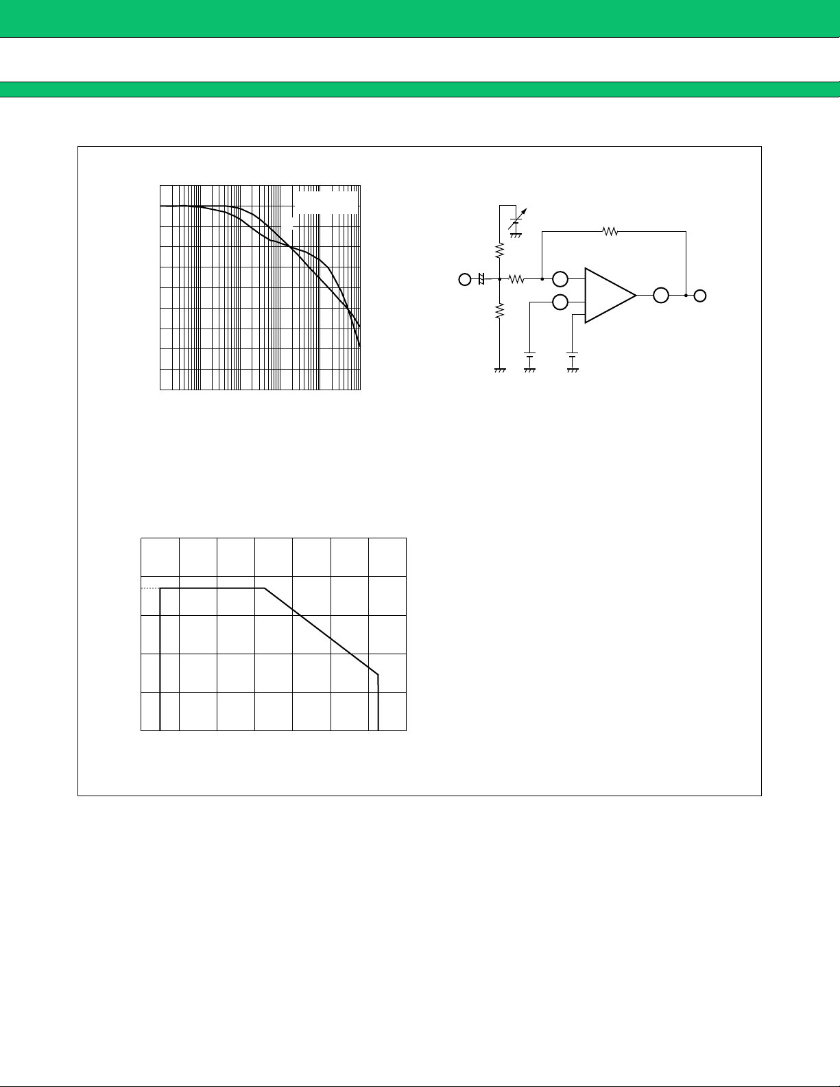
Conversion Efficiency
100
90
80
70
60
50
40
vs. Load Current (CH1)
Conversion efficiency η (%)
30
10 m 100 m 1 10
Load current IL (A)
Conversion Efficiency
vs. Load Current (CH2)
Ta = +25 °C
5 V Output
SW1 = OFF
SW2 = ON
VIN = 7 V
V
IN = 10 V
V
IN = 12 V
VIN = 19 V
100
90
80
70
60
50
40
Conversion efficiency η (%)
30
10 m 100 m 1 10
Load current IL (A)
Ta = +25 °C
3.3 V Output
SW1 = ON
SW2 = OFF
VIN = 7 V
V
IN = 10 V
V
IN = 12 V
VIN = 19 V
(Continued)
32
Page 33

(Continued)
MB39A104
Switching Wave Form (CH1)
VG (V)
V
S (V)
VG (V)
15
10
15
10
5
0
15
10
5
0
012345678910
Switching Wave Form (CH2)
5
Ta = +25 °C
IN = 12 V
V
CTL = 5 V
V
O = 5 V
RL = 1.67 Ω
t (µs)
Ta = +25 °C
IN = 12 V
V
CTL = 5 V
O = 3.3 V
V
RL = 1.1 Ω
V
S (V)
0
15
10
5
0
012345678910
t (µs)
33
Page 34

MB39A104
■ USAGE PRECAUTIONS
• Printed circuit board ground lines should be set up with consideration for common impedance.
• Take appropriate static electricity measures.
• Containers for semiconductor materials should have anti-static protection or be made of conductive material.
• After mounting, printed circuit boards should be stored and shipped in conductive bags or containers.
• Work platforms, tools, and instruments should be properly grounded.
• Working personnel should be grounded with resistance of 250 kΩ to 1 MΩ between body and ground.
• Do not apply negative voltages.
• The use of negative voltages below −0.3 V may create parasitic transistors on LSI lines, which can cause
malfunction.
■ ORDERING INFORMATION
Part number Package Remarks
MB39A104PFV-❏❏❏E1
■ EV BOARD ORDERING INFORMATION
EV board part No. EV board version No. Remarks
MB39A104EVB Board Rev. 1.0 SSOP-24P
■ RoHS COMPLIANCE INFORMATION OF LEAD (Pb) FREE VERSION
The LSI products of Fujitsu Microelectronics with “E1” are compliant with RoHS Directive , and has observed
the standard of lead, cadmium, mercury, Hexavalent chromium, polybrominated biphenyls (PBB) , and polybrominated diphenyl ethers (PBDE) .
The product that conforms to this standard is added “E1” at the end of the part number.
■ MARKING FORMAT (Lead Free version)
24-pin plastic SSOP
(FPT-24P-M03)
3
19A 04
Lead Free version
XXXX
34
INDEX
XXX
E1
Lead Free version
Page 35

■ LABELING SAMPLE (LEAD FREE VERSION)
MB123456P - 789 - GE1
(3N) 1MB123456P-789-GE1
1000
lead-free mark
JEITA logo JEDEC logo
G
Pb
MB39A104
(3N)2 1561190005 107210
1,000
PCS
MB123456P - 789 - GE1
2006/03/01
MB123456P - 789 - GE1
1561190005
QC PASS
ASSEMBLED IN JAPAN
1/1
0605 - Z01A
Lead Free version
1000
35
Page 36

MB39A104
■ MB39A104PFV-❏❏❏E1
RECOMMENDED CONDITIONS OF MOISTURE SENSITIVITY LEVEL
Item Condition
Mounting Method IR (infrared reflow) , Manual soldering (partial heating method)
Mounting times 2 times
Before opening
Storage period
From opening to the 2nd
reflow
When the storage period after
opening was exceeded
Storage conditions 5 °C to 30 °C, 70%RH or less (the lowest possible humidity)
[Temperature Profile for FJ Standard IR Reflow]
(1) IR (infrared reflow)
H rank : 260 °C Max
260 °C
Please use it within two years after
Manufacture.
Less than 8 days
Please processes within 8 days
after baking (125 °C, 24H)
255 °C
170 °C
to
190 °C
RT
(a)
(b)
(c)
(d)
(d')
(e)
(a) Temperature Increase gradient : Average 1 °C/s to 4 °C/s
(b) Preliminary heating : Temperature 170 °C to 190 °C, 60 s to 180 s
(c) Temperature Increase gradient : Average 1 °C/s to 4 °C/s
(d) Actual heating : Temperature 260 °C Max; 255 °C or more, 10 s or less
(d’) : Temperature 230 °C or more, 40 s or less
or
Temperature 225 °C or more, 60 s or less
or
Temperature 220 °C or more, 80 s or less
(e) Cooling : Natural cooling or forced cooling
Note : Temperature : the top of the package body
(2) Manual soldering (partial heating method)
Conditions : Temperature 400 °C Max
Times : 5 s max/pin
36
Page 37

■ PACKAGE DIMENSION
24-pin plastic SSOP Lead pitch 0.65 mm
MB39A104
(FPT-24P-M03)
24-pin plastic SSOP
(FPT-24P-M03)
1
*
7.75±0.10(.305±.004)
Package width
package length
×
5.6 × 7.75 mm
Lead shape Gullwing
Sealing method Plastic mold
Mounting height 1.45 mm MAX
Weight 0.12 g
Code
(Reference)
Note 1)*1 : Resin protrusion. (Each side : +0.15 (.006) Max).
Note 2)*2 : These dimensions do not include resin protrusion.
Note 3) Pins width and pins thickness include plating thickness.
Note 4) Pins width do not include tie bar cutting remainder.
0.17±0.03
1324
(.007±.001)
P-SSOP24-5.6×7.75-0.65
INDEX
112
0.65(.026)
C
2003 FUJITSU LIMITED F24018S-c-4-5
0.24
.009
0.10(.004)
0.10(.004)
+0.08
–0.07
+.003
–.003
2
5.60±0.10 7.60±0.20
*
(.220±.004) (.299±.008)
0.13(.005)
M
Details of "A" part
+0.20
–0.10
1.25
(Mounting height)
+.008
.049
–.004
0.25(.010)
0~8
"A"
Dimensions in mm (inches).
Note: The values in parentheses are reference values.
˚
0.50±0.20
(.020±.008)
0.60±0.15
(.024±.006)
0.10±0.10
(.004±.004)
(Stand off)
37
Page 38

MB39A104
MEMO
38
Page 39

MEMO
MB39A104
39
Page 40

FUJITSU MICROELECTRONICS LIMITED
Shinjuku Dai-Ichi Seimei Bldg. 7-1, Nishishinjuku 2-chome, Shinjuku-ku,
Tokyo 163-0722, Japan Tel: +81-3-5322-3347 Fax: +81-3-5322-3387
http://jp.fujitsu.com/fml/en/
For further information please contact:
North and South America
FUJITSU MICROELECTRONICS AMERICA, INC.
1250 E. Arques Avenue, M/S 333
Sunnyvale, CA 94085-5401, U.S.A.
Tel: +1-408-737-5600 Fax: +1-408-737-5999
http://www.fma.fujitsu.com/
Europe
FUJITSU MICROELECTRONICS EUROPE GmbH
Pittlerstrasse 47, 63225 Langen,
Germany
Tel: +49-6103-690-0 Fax: +49-6103-690-122
http://emea.fujitsu.com/microelectronics/
Korea
FUJITSU MICROELECTRONICS KOREA LTD.
206 KOSMO TOWER, 1002 Daechi-Dong,
Kangnam-Gu,Seoul 135-280
Korea
Tel: +82-2-3484-7100 Fax: +82-2-3484-7111
http://www.fmk.fujitsu.com/
Asia Pacific
FUJITSU MICROELECTRONICS ASIA PTE LTD.
151 Lorong Chuan, #05-08 New Tech Park,
Singapore 556741
Tel: +65-6281-0770 Fax: +65-6281-0220
http://www.fujitsu.com/sg/services/micro/semiconductor/
FUJITSU MICROELECTRONICS SHANGHAI CO., LTD.
Rm.3102, Bund Center, No.222 Yan An Road(E),
Shanghai 200002, China
Tel: +86-21-6335-1560 Fax: +86-21-6335-1605
http://cn.fujitsu.com/fmc/
FUJITSU MICROELECTRONICS PACIFIC ASIA LTD.
10/F., World Commerce Centre, 11 Canton Road
Tsimshatsui, Kowloon
Hong Kong
Tel: +852-2377-0226 Fax: +852-2376-3269
http://cn.fujitsu.com/fmc/tw
All Rights Reserved.
The contents of this document are subject to change without notice.
Customers are advised to consult with sales representatives before ordering.
The information, such as descriptions of function and application circuit examples, in this document are presented solely for the purpose
of reference to show examples of operations and uses of FUJITSU MICROELECTRONICS device; FUJITSU MICROELECTRONICS
does not warrant proper operation of the device with respect to use based on such information. When you develop equipment incorporating the device based on such information, you must assume any responsibility arising out of such use of the information.
FUJITSU MICROELECTRONICS assumes no liability for any damages whatsoever arising out of the use of the information.
Any information in this document, including descriptions of function and schematic diagrams, shall not be construed as license of the use
or exercise of any intellectual property right, such as patent right or copyright, or any other right of FUJITSU MICROELECTRONICS
or any third party or does FUJITSU MICROELECTRONICS warrant non-infringement of any third-party's intellectual property right or
other right by using such information. FUJITSU MICROELECTRONICS assumes no liability for any infringement of the intellectual
property rights or other rights of third parties which would result from the use of information contained herein.
The products described in this document are designed, developed and manufactured as contemplated for general use, including without
limitation, ordinary industrial use, general office use, personal use, and household use, but are not designed, developed and manufactured
as contemplated (1) for use accompanying fatal risks or dangers that, unless extremely high safety is secured, could have a serious effect
to the public, and could lead directly to death, personal injury, severe physical damage or other loss (i.e., nuclear reaction control in
nuclear facility, aircraft flight control, air traffic control, mass transport control, medical life support system, missile launch control in
weapon system), or (2) for use requiring extremely high reliability (i.e., submersible repeater and artificial satellite).
Please note that FUJITSU MICROELECTRONICS will not be liable against you and/or any third party for any claims or damages arising
in connection with above-mentioned uses of the products.
Any semiconductor devices have an inherent chance of failure. You must protect against injury, damage or loss from such failures by
incorporating safety design measures into your facility and equipment such as redundancy, fire protection, and prevention of over-current
levels and other abnormal operating conditions.
Exportation/release of any products described in this document may require necessary procedures in accordance with the regulations of
the Foreign Exchange and Foreign Trade Control Law of Japan and/or US export control laws.
The company names and brand names herein are the trademarks or registered trademarks of their respective owners.
Edited Strategic Business Development Dept.
 Loading...