

Page 1

FUJITSU SEMICONDUCTOR
DATA SHEET
DS04-27706-2E
ASSP
For Power Supply Applications (Secondary battery)
DC/DC Converter IC for Charging
MB3878
DESCRIPTION
■■■■
The MB3878 is a DC/DC converter IC suitable for down-conversion, using pulse-width (PWM) charging and
enabling output voltage to be set to any desired level from one cell to four cells.
These ICs can dynamically control the secondary batter y’s charge current by detecting a voltage drop in an AC
adaptor in order to keep its power constant (dynamically-controlled charging).
The charging method enables quick charging, f or example, with the A C adaptor during operation of a notebook PC
The MB3878 provides a broad power supply voltage range and low standby current as well as high efficiency,
making it ideal for use as a built-in charging device in products such as notebook PC.
This product is covered by US Patent Number 6,147,477.
FEATURES
■■■■
• Detecting a voltage drop in the AC adaptor and dynamically controlling the charge current
(Dynamically-controlled charging)
• Output voltage setting using external resistor : 1 cell to 4 cells
• High efficiency : 94 %
• Wide range of operating supply voltages : 7 V to 25 V
• Output voltage setting accuracy : 4.2V ± 0.8% (per cell)
• Built-in frequency setting capacitor enables frequency setting using external resistor only
• Oscillator frequency range : 100kHz to 500kHz
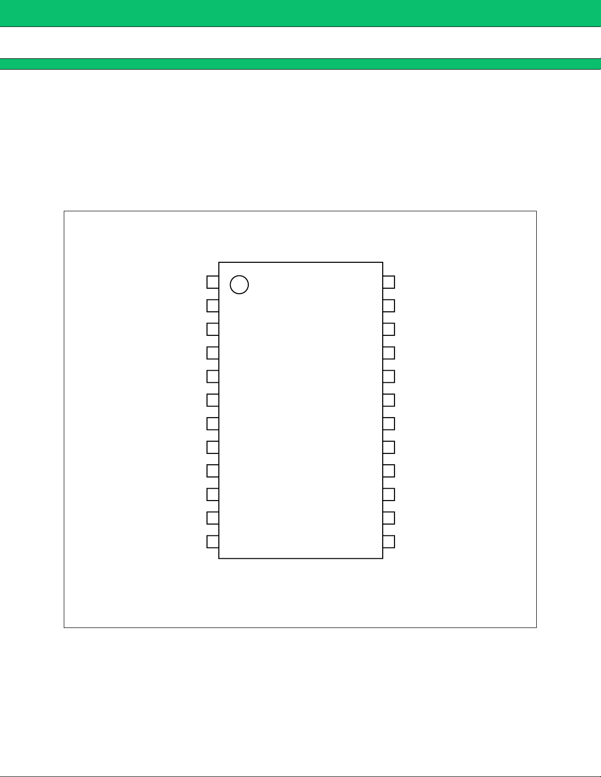
PACKAGE
■■■■
24-pin plastic SSOP
(FPT-24P-M03)
(Continued)
Page 2
MB3878
(Continued)
• Built-in current detector amplifier with wide in-phase input voltage range : 0 V to Vcc
• In standby mode, leave output voltage setting resistor open to prevent inefficient current loss
• Built-in standby current function : 0 µA (standard)
• Built-in soft-start function
• Built-in totem-pole output stage supporting P-channel MOS FETs devices
PIN ASSIGNMENT
■■■■
(TOP VIEW)
: +INC2
−INC2 :
OUTC2 :
+INE2 :
1
2
3
24
23
22
: GND
: CS
−INE2 :
FB2 :
VREF :
FB1 :
−INE1 :
+INE1 :
OUTC1 :
OUTD :
−INC1 :
10
11
12
: VCC (O)
4
5
6
7
8
9
21
20
19
18
17
16
15
14
13
: OUT
: VH
: VCC
: RT
: −INE3
: FB3
: CTL
: +INC1
(FPT-24P-M03)
2
Page 3

PIN DESCRIPTION
■■■■
Pin No. Symbol I/O Descriptions
1 −INC2 I Current detection amplifier (Current Amp. 2) input pin.
2 OUTC2 O Current detection amplifier (Current Amp. 2) output pin.
3 +INE2 I Error amplifier (Error Amp. 2) non-inverted input pin.
4 −INE2 I Error amplifier (Error Amp. 2) inverted input pin.
5 FB2 O Error amplifier (Error Amp. 2) output pin.
6 VREF O Reference voltage output pin.
7 FB1 O Error amplifier (Error Amp. 1) output pin.
8 −INE1 I Error amplifier (Error Amp. 1) inverted input pin
9 +INE1 I Error amplifier (Error Amp. 3) non-inverted input pin.
10 OUTC1 O Current detection amplifier (Current Amp. 1) output pin.
With IC in standby mode, this pin is left open to prevent loss of current
11 OUTD O
12 −INC1 I Current detector amplifier (Current Amp. 1) input pin.
through output voltage setting resistance. Set CTL pin to “H” level and
OUTD pin to “L” level.
MB3878
13 +INC1 I Current detector amplifier (Current Amp. 1) input pin.
14 CTL I
15 FB3 O Error amplifier (Error Amp. 3) output pin.
16 −INE3 I Error amplifier (Error Amp. 3) inverted input pin.
17 RT Triangular-wave oscillation frequency setting resistor connection pin.
18 VCC Power supply pin for reference power supply and control circuit.
19 VH O Power supply pin for FET drive circuit (VH = Vcc − 5 V).
20 OUT O High-side FET gate drive pin.
21 VCC (O) Output circuit power supply pin.
22 CS Soft-start capacitor connection pin.
23 GND Ground pin.
24 +INC2 I Current detection amplifier (Current Amp. 2) input pin.
Power supply control pin.
Setting the CTL pin low places the IC in the standby mode.
3
Page 4
MB3878
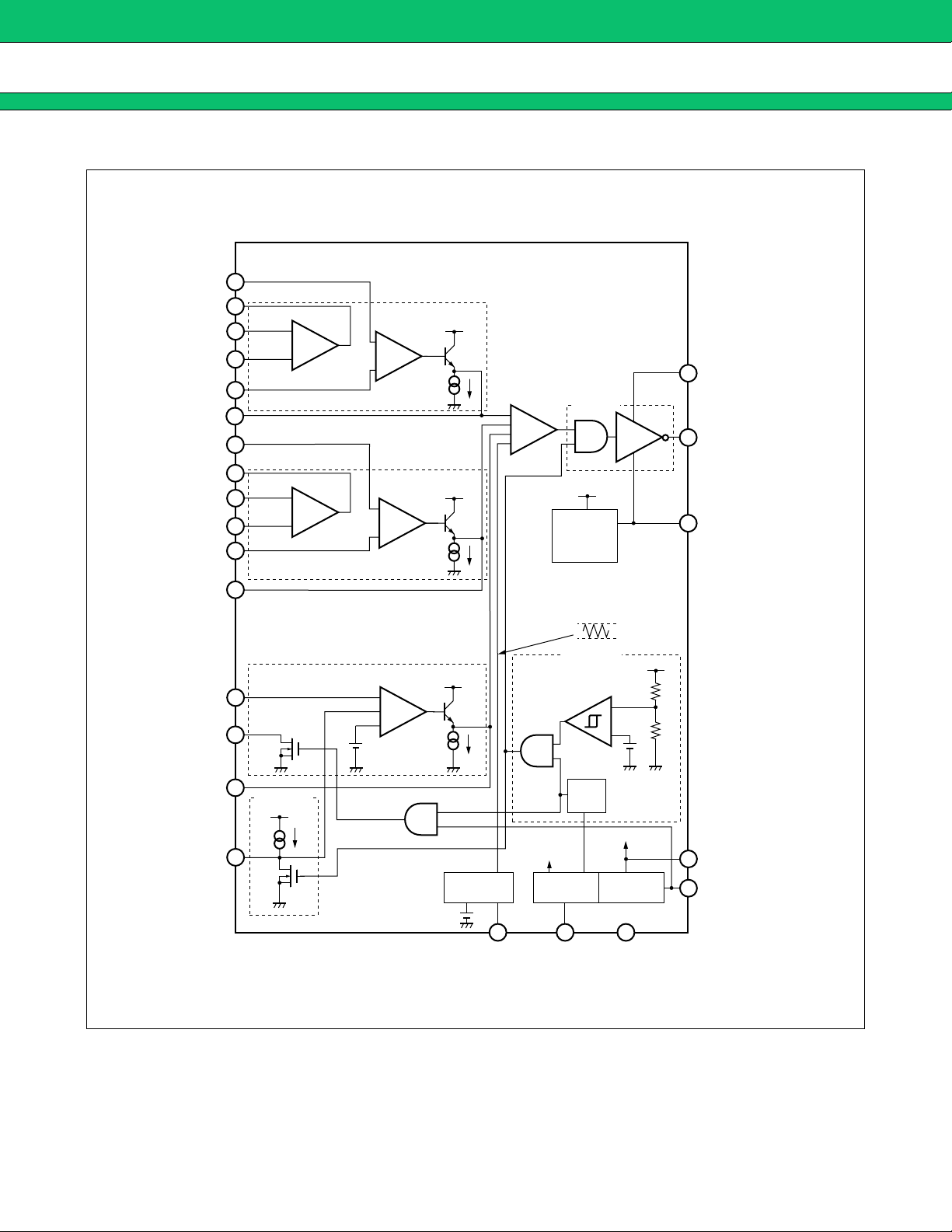
BLOCK DIAGRAM
■■■■
−INE1
OUTC1
+INC1
−INC1
+INE1
FB1
−INE2
8
10
<Current Amp.1>
13
12
9
7
4
+
× 25
−
<Error
Amp.1>
−
+
VREF
<PWM Comp.>
+
+
+
−
<OUT>
Drive
21
20
VCC (O)
OUT
OUTC2
+INC2
−INC2
+INE2
FB2
−INE3
OUTD
FB3
CS
2
<Current Amp.2>
24
1
3
5
16
11
15
<SOFT>
VREF
22
+
× 25
−
1 µA
<Error
Amp.2>
−
+
<Error
Amp.3>
−
+
+
4.2 V
VREF
VREF
(45 pF)
(VCC UVLO)
bias
<OSC>
17 6 23
RT
<REF> <CTL>
VREF
VCC
Bias
Voltage
<VH>
<UVLO>
0.91 V
(0.77 V)
VREF
UVLO
VREF
5.0 V
(V
2.5 V
1.5 V
215 kΩ
+
35 kΩ
−
VCC
GND
CC − 5 V)
VCC
19
18
14
VH
VCC
CTL
4
Page 5
ABSOLUTE MAXIMUM RAGINGS
■■■■
MB3878
Parameter Symbol Conditions
Unit
Min Max
Power supply voltage VCC VCC, VCC (O) 28 V
Rating
Output current I
Peak output current I
OUT 60 mA
OUT Duty ≤ 5 % (t = 1 / fOSC × Duty) 500 mA
Power dissipation PD Ta ≤ +25 °C 740* mW
Storage temperature Tstg −55 +125 °C
* : The package is mounted on the dual-sided epoxy board (10 cm × 10 cm).
WARNING: Semiconductor devices can be permanently damaged by application of stress (voltage, current,
temperature, etc.) in excess of absolute maximum ratings. Do not exceed these ratings.
RECOMMENDED OPERATING CONDITIONS
■■■■
Value
Parameter
Symbol
Conditions
Min Typ Max
Power supply voltage V
Reference voltage output
current
VH pin output current I
CC VCC, VCC (O) 7 25 V
I
REF −1 0mA
VH 0 30 mA
VINE −INE1 to −INE3, +INE1, +INE2 0 VCC − 1.8 V
Input voltage
V
INC +INC1, +INC2, −INC1, −INC2 0 VCC V
Unit
OUTD pin output voltage V
OUTD pin output current I
OUTD 0 17 V
OUTD 0 2mA
CTL pin input voltage VCTL 0 25 V
output current I
Peak output current I
OUT −45 45 mA
OUT Duty ≤ 5 % (t = 1 / fosc × Duty) −450 450 mA
Oscillator frequency fOSC 100 290 500 kHz
Timing resistor R
Soft-start capacitor C
T 33 47 130 kΩ
S 2200 100000 pF
VH pin capacitor CVH 0.1 1.0 µF
Reference voltage output
capacitor
C
REF 0.1 1.0 µF
Operating ambient temperature Ta −30 +25 +85 °C
WARNING: The recommended operating conditions are required in order to ensure the normal operation of the
semiconductor device. All of the device’s electrical characteristics are warranted when the device is
operated within these ranges.
Always use semiconductor devices within their recommended operating condition ranges. Operation
outside these ranges may adversely affect reliability and could result in device failure.
No warranty is made with respect to uses, operating conditions, or combinations not represented on
the data sheet. Users considering application outside the listed conditions are advised to contact their
FUJITSU representatives beforehand.
5
Page 6
MB3878
ELECTRICAL CHARACTERISTICS
■■■■
Parameter Symbol
(Ta = +25 °C, VCC = 19 V, VCC (O) = 19 V, VREF = 0 mA)
Pin
No.
Conditions
Min Typ Max
Value
Unit
Reference
voltage block
(Ref)
Under voltage
lockout protection
circuit block
(UVLO)
Soft-start block
(SOFT)
Triangular
waveform
oscillator circuit
block (OSC)
Output voltage V
REF 6
Ta = −30 °C to +85 °C 4.945 5.000 5.055 V
Input stability Line 6 VCC = 7 V to 25 V 310mV
Load stability Load 6 VREF = 0 mA to −1 mA 110mV
Ta = +25 °C 4.995 5.000 5.045 V
Short-circuit
output current
Ios 6 VREF = 1 V −25 −15 −5mA
TLH 18
V
VCC = VCC (O) ,
VCC =
6.1 6.4 6.7 V
Threshold voltage
V
THL 18
VCC = VCC (O) ,
VCC =
5.1 5.4 5.7 V
Hysteresis width VH 18 VCC = VCC (O) 0.7 1.0 1.3 V
TLH 6VREF = 2.6 2.8 3.0 V
V
Threshold voltage
V
THL 6VREF = 2.4 2.6 2.8 V
Hysteresis width VH 6VH = VTLH − VTHL 0.05 0.20 0.35 V
Charge current I
Oscillation
frequency
CS 22 −1.3 −0.8 −0.5 µA
OSC 20 RT = 47 kΩ 260 290 320 kHz
f
Frequency
temperature
∆f/fdt 20 Ta = −30 °C to +85 °C 1* %
stability
Input offset
voltage
V
3, 4,
IO
FB1 = FB2 = 2 V 15mV
8, 9
Error amplifier
block
(Error Amp.1,
Error Amp.2)
* : Standard design value.
6
Input bias current I
Common mode
input voltage
V
range
Voltage gain A
Frequency
bandwidth
V
Output voltage
VFBL 5, 7 20 200 mV
Output source
current
Output sink
current
I
SOURCE 5, 7 FB1 = FB2 = 2 V −2.0 −0.6 mA
I
3, 4,
B
8, 9
3, 4,
CM
8, 9
V 5, 7 DC 100* dB
B
W 5, 7 AV = 0 dB 2.0* MHz
FBH 5, 7 4.7 4.9 V
SINK 5, 7 FB1 = FB2 = 2 V 150 300 µA
−100 −30 nA
0
VCC −
1.8
(Continued)
V
Page 7

Parameter Symbol
TH1 16 FB3 = 2 V, Ta = +25 °C 4.167 4.200 4.233 V
V
Threshold voltage
V
TH2 16
Input current I
INE3 16 −INE3 = 0 V −100 −30 nA
MB3878
(Ta = +25 °C, VCC = 19 V, VCC (O) = 19 V, VREF = 0 mA)
Pin
No.
Conditions
FB3 = 2 V,
Ta = −30 °C to +85 °C
Min Typ Max
4.158 4.200 4.242 V
Value
Unit
Error amplifier
block
(Error Amp.3)
Current
detection
amplifier block
(Current Amp.1,
Current Amp.2)
Voltage gain A
Frequency
bandwidth
V
Output voltage
V
Output source
current
Output sink current
OUTD pin output
leak current
OUTD pin output
ON resistor
SOURCE 15 FB3 = 2 V −2.0 −0.6 mA
I
ISINK 15 FB3 = 2 V 150 300 µA
I
R
+INCH
I
−INCH
I
Input current
+INCL
I
−INCL
I
OUTC1
V
OUTC2
Current detection
voltage
V
V
V
OUTC3
OUTC4
Common mode
input voltage
VCM
range
V 15 DC 100* dB
W 15 AV = 0 dB 2.0* MHz
B
FBH 15 4.7 4.9 V
FBL 15 20 200 mV
LEAK 11 OUTD = 16.8 V 01µA
ON 11 OUTD = 1 mA 70 100 Ω
+INC1 = +INC2 = 12.7 V,
13,
−INC1 = −INC2 = 12.6 V
24
+INC1 = +INC2 = 12.7 V,
1,
−INC1 = −INC2 = 12.6 V
12
+INC1 = +INC2 = 0.1 V,
13,
−INC1 = −INC2 = 0 V
24
+INC1 = +INC2 = 0.1 V,
1,
−INC1 = −INC2 = 0 V
12
+INC1 = +INC2 = 12.7 V,
2,
−INC1 = −INC2 = 12.6 V
10
+INC1 = +INC2 = 12.63 V,
2,
−INC1 = −INC2 = 12.6 V
10
+INC1 = +INC2 = 0.1 V,
2,
−INC1 = −INC2 = 0 V
10
+INC1 = +INC2 = 0.03 V,
2,
−INC1 = −INC2 = 0 V
10
10 20 µA
0.1 0.2 µA
−130 −65 µA
−140 −70 µA
2.25 2.5 2.75 V
0.50 0.75 1.00 V
1.25 2.50 3.75 V
0.125 0.750 1.375 V
1,
12,
13,
0 Vcc V
24
Voltage gain A
Frequency
bandwidth
* : Standard design value.
2,
V
B
W
+INC1 = +INC2 = 12.7 V,
−INC1 = −INC2 = 12.6 V
10
2,
AV = 0 dB 2.0* MHz
10
22.5 25 27.5 V/V
(Continued)
7
Page 8

MB3878
(Continued)
Parameter Symbol
Current detection
amplifier block
(Current Amp.1,
Current Amp.2)
PWM comparator
block
(PWM Comp.)
Output voltage
Output source
current
Output sink
current
Threshold voltage
Output source
current
(Ta = +25 °C, VCC = 19 V, VCC (O) = 19 V, VREF = 0 mA)
Pin
No.
OUTCH 2, 10 4.7 4.9 V
V
V
OUTCL 2, 10 20 200 mV
I
SOURCE 2, 10 OUTC1 = OUTC2 = 2 V −2.0 −0.6 mA
Conditions
Min Typ Max
Value
Unit
ISINK 2, 10 OUTC1 = OUTC2 = 2 V 150 300 µA
5, 7,
TL
V
V
TH
I
SOURCE 20
Duty cycle = 0 % 1.4 1.5 V
15
5, 7,
Duty cycle = 100 %2.5 2.6 V
15
OUT = 11 V, Duty ≤ 5 %
(t = 1 / fOSC × Duty)
−200* mA
Output block
(OUT)
Control block
(CTL)
Bias voltage
block (VH)
General
Output sink
current
Output ON
resistor
I
SINK 20
R
OH 20 OUT = −45 mA 8.0 12.0 Ω
ROL 20 OUT = 45 mA 6.5 9.7 Ω
Rise time tr1 20
Fall time tf1 20
ON 14 Active mode 2 25 V
V
CTL input voltage
VOFF 14 Standby mode 0 0.8 V
CTLH 14 CTL = 5 V 100 200 µA
I
Input current
I
CTLL 14 CTL = 0 V 01µA
Output voltage VH 19
Standby current I
Power supply
current
CCS
I
CC
18, 19VCC = VCC (O) ,
18, 19VCC = VCC (O) ,
OUT = 16 V, Duty ≤ 5 %
(t = 1 / fOSC × Duty)
OUT = 3300 pF
(equivalent to Si4435 × 1)
OUT = 3300 pF
(equivalent to Si4435 × 1)
VCC = VCC (O)
= 7 V to 25 V,
VH = 0 to 30 mA
CTL = 0 V
CTL = 5 V
200* mA
70* ns
60* ns
VCC −
5.5
VCC −
5.0
VCC −
4.5
010µA
8.0 12.0 mA
V
* : Standard design value
8
Page 9

TYPICAL CHARACTERISTICS
■■■■
MB3878
Power supply current vs. power supply voltage
12
10
8
6
CC (mA)
I
4
2
Power supply current
0
0 5 10 15 20 25
Power supply voltage V
Ta = +25 °C
CTL = 5 V
CC (V)
Reference voltage vs. VREF load current
10
8
6
4
2
Ta = +25 °C
VCC = 19 V
CTL = 5 V
Reference voltage VREF (V)
0
0 5 10 15 20 25 30
VREF load current IREF (mA)
Reference voltage vs. power supply voltage
10
8
6
4
2
Reference voltage VREF (V)
0
0 5 10 15 20 25
Ta = +25 °C
CTL = 5 V
VREF = 0 mA
Power supply voltage VCC (V)
Reference voltage vs. ambient temperature
2.0
1.5
1.0
0.5
0.0
−0.5
−1.0
−1.5
Reference voltage ∆VREF (%)
−2.0
−40 −20 0 20 40 60 80 100
VCC = 19 V
CTL = 5 V
VREF = 0 mA
Ambient temperature Ta ( °C)
Reference voltage vs. CTL pin voltage
10
8
6
4
2
Ta = +25 °C
VCC = 19 V
VREF = 0 mA
Reference voltage VREF (V)
0
0 0.5 1 1.5 2 2.5
CTL pin voltage VCTL (V)
CTL pin current vs. CTL pin voltage
1.0
Ta = +25 °C
VCC = 19 V
0.8
0.6
0.4
0.2
CTL pin current ICTL (mA)
0.0
0 5 10 15 20 25
CTL pin voltage VCTL (V)
(Continued)
9
Page 10

MB3878
Triangular wave oscillator frequency vs.
timing resistor
1 M
100 k
OSC (Hz)
f
10 k
Triangular wave oscillator frequency
10 k 100 k 1 M
Timing resistor R
Triangular wave oscillator frequency
340
330
320
310
300
290
OSC (kHz)
280
270
260
frequency f
250
Triangular wave oscillator
240
−40 −20 0 20 40 60 80 100
Ta = +25 °C
VCC = 19 V
CTL = 5 V
T (Ω)
VCC = 19 V
CTL = 5 V
RT = 47 kΩ
Triangular wave oscillator frequency vs.
power supply voltage
340
330
320
310
300
290
280
OSC (kHz)
f
270
260
250
240
Triangular wave oscillator frequency
0 5 10 15 20 25
Power supply voltage VCC (V)
Error amplifier threshold voltage vs.
ambient temperature (Error Amp.3)
5.0
4.0
3.0
2.0
1.0
0.0
−1.0
−2.0
−3.0
−4.0
−5.0
−40 −20 0 20 40 60 80 100
Ta = +25 °C
CTL = 5 V
RT = 47 kΩ
VCC = 19 V
CTL = 5 V
10
Ambient temperature Ta ( °C)
Error amplifier threshold voltage ∆VTH (%)
Ambient temperature Ta ( °C)
(Continued)
Page 11

(Continued)
MB3878
Error amplifier gain and phase vs. frequency
40
20
0
Gain AV (dB)
−20
−40
1 k 10 k 100 k 1 M 10 M
AV
φ
Ta = +25 °C
Frequency f (Hz)
Current detection amplifier gain and phase
vs. frequency
40
20
Gain AV (dB)
−20
−40
φ
AV
0
Ta = +25 °C
180
90
0
−90
−180
180
90
0
−90
−180
IN
Phase φ (deg)
Phase φ (deg)
1 µF
−+
5.2 V
10 kΩ
2.4 kΩ
10 kΩ
VCC = 19 V
240 kΩ
8
−
(4)
+
9
(3)
2.5 V
VCC = 19 V
13
+
(24)
×25
−
12
(1)
12.55 V12.6 V
OUT
7
(5)
Error Amp.1
(Error Amp.2)
OUT
10
(2)
Current Amp.1
(Current Amp.2)
1 k 10 k 100 k 1 M 10 M
Frequency f (Hz)
Power dissipation vs. ambient temperature
800
740
700
600
500
400
300
200
100
Power dissipation PD (mW)
0
−40 −20 0 20 40 60 80 100
Ambient temperature Ta ( °C)
11
Page 12

MB3878
FUNCTIONAL DESCRIPTION
■■■■
1. DC/DC Converter Unit
(1) Reference voltage block (Ref)
The reference voltage generator uses the voltage supplied from the VCC terminal (pin 18) to generate a temperature-compensated, stable voltage (5.0V Typ) used as the reference supply voltage for the IC’s internal
circuitry.
This pin can also be used to obtain a load current to a maximum of 1mA from the reference voltage VREF
terminal (pin 6).
(2) Triangular wave oscillator block (OSC)
The triangular wave oscillator b uilds the capacitor for frequency setting into, and generates the triangular wave
oscillator waveform by connecting the frequency setting resistor with the RT terminal (pin 17).
The triangular wave is input to the PWM comparator on the IC.
(3) Error amplifier block (Error Amp.1)
This amplifier detects the output signal from the current detector ampifier (Current amp .1), compares this to the
+INE1 terminal (pin 9), and outputs a PWM control signal to be used in controlling the charging current.
In addition, an arbitrary loop gain can be set up by connecting a feedback resistor and capacitor between the
FB1 terminal (pin 7) and -INE terminal (pin 8), providing stable phase compensation to the system.
(4) Error amplifier block (Error Amp.2)
This amplifier (Error Amp.2) detects voltage pendency of the AC adaptor and outputs a PWM control signal.
In addition, an arbitrary loop gain can be set by connecting a feedback resistor and capacitor from the FB2
terminal (pin 5) to the -INE2 terminal (pin 4) of the error amplifier, enabling stable phase compensation to the
system.
(5) Error amplifier block (Error Amp.3)
This error amplifier (Error Amp. 3) detects the output voltage from the DC/DC converter and outputs the PWM
control signal. External output voltage setting resistors can be connected to the error amplifier inverse input pin
to set the desired level of output voltage from 1 cell to 4 cells.
In addition, an arbitrary loop gain can be set by connecting a feedback resistor and capacitor from the FB3
terminal (pin 15) to the −INE3 terminal (pin 16) of the error amplifier, enabling stable phase compensation to the
system.
Connecting a soft-start capacitor to the CS terminal (pin 22) prevents surge currents when the IC is turned on.
Using an error amplifier for soft-start detection makes the soft-start time constant, independent of the output load.
(6) Current detector amplifier block (Current Amp.1)
The current detection amplifier (Current Amp.1) detects a voltage drop which occurs between both ends of the
output sense resistor (R
−INC1 terminal (pin 12). Then it outputs the signal amplified by 25 times to the error amplifier (Error Amp.1) at
the next stage.
12
S) due to the flow of the charge current, using the +INC1 terminal (pin 13) and
Page 13

MB3878
(7) PWM comparator block (PWM Comp.)
The PWM comparator circuit is a voltage-pulse width conver ter for controlling the output duty of the error
amplifiers (Error Amp. 1 to Error Amp. 3) depending on their output voltage.
The PWM comparator circuit compares the triangular wave generated by the triangular wave oscillator to the
error amplifier output voltage and turns on the external output transistor during the interval in which the triangular
wave voltage is lower than the error amplifier output voltage.
(8) Output block (OUT)
The output circuit uses a totem-pole configuration capable of driving an external P-channel MOS FET.
The output “L” level sets the output amplitude to 5 V (Typ) using the voltage generated by the bias v oltage b lock
(VH).
This results in increasing conversion efficiency and suppressing the withstand v oltage of the connected external
transistor in a wide range of input voltages.
(9) Control block (CTL)
Setting the CTL terminal (pin 14) low places the IC in the standby mode. (The supply current is 10 µA at maximum
in the standby mode.)
(10) Bias voltage block (VH)
The bias voltage circuit outputs Vcc − 5 V (Typ) as the minimum potential of the output circuit. In the standby
mode, this circuit outputs the potential equal to Vcc.
2. Protection Functions
Under voltage lockout protection circuit (UVLO)
The transient state or a momentary decrease in supply voltage or internal reference voltage (VREF), which
occurs when the power supply is turned on, may cause malfunctions in the control IC, resulting in breakdown
or degradation of the system. To prevent such malfunction, the under voltage lockout protection circuit detects
a supply voltage or internal reference voltage drop and fixes the OUT terminal (pin 20) to the “H” level. The
system restores voltage supply when the supply voltage or internal reference voltage reaches the threshold
voltage of the under voltage lockout protection circuit.
3. Soft-start Function
Soft-start block (SOFT)
Connecting a capacitor to the CS terminal (pin 22) prevents surge currents when the IC is turned on. Using an
error amplifier for soft-start detection makes the soft-start time constant, independent of the output load of the
DC/DC converter.
13
Page 14

MB3878
SETTING THE CHARGING VOLTAGE
■■■■
The charging voltage (DC/DC output voltage) can be set by connecting external voltage setting resistors (R3,
R4) to the -INE3 terminal. Be sure to select a resistor value that allows you to ignore the on resistor (70 Ω, 1mA)
of the internal FET connected to the OUTD terminal (pin 11).
Battery charging voltage: V
O
VO (V) = (R3 + R4) / R4 × 4.2 (V)
O
V
B
R3
−INE3
16
R4
11
OUTD
22
CS
< Error Amp.3 >
−
+
+
4.2 V
METHOD OF SETTING THE CHARGING CURRENT
■■■■
The charge current (output control current) value can be set with the voltage at the +INE1 terminal (pin 9).
If a current exceeding the set value attempts to flo w , the charge v oltage drops according to the set current value.
Battery charge current setting voltage : +INE1
+INE1 (V) = 25 × I1 (A) × R
METHOD OF SETTING THE SOFT-START TIME
■■■■
S (Ω)
Upon activation, the IC starts charging the capacitor (Cs) connected to the CS terminal (pin 22).
The error amplifier causes soft-start operation to be performed with the output voltage in proportion to the CS
terminal voltage regardless of the load current of the DC/DC converter.
Soft-start time: ts (Time taken for the output voltage to reach 100 %)
ts (s) := 4.2 × C
METHOD OF SETTING THE TRIANGULAR WAVE OSCILLATOR FREQUENCY
■■■■
S (µF)
The trianguar wave oscillator frequency can be set b y the timing resistor (RT) connected the RT terminal (pin 17).
Triangular wave oscillator frequency: f
OSC
fOSC (kHz) := 13630 / RT (kΩ)
14
Page 15

MB3878
AC ADAPTOR VOLTAGE DETECTION
■■■■
With an external resistor connected to the +INE2 terminal(pin 3), the IC enters the dynamically-controlled
charging mode to reduce the charge current to keep AC adaptor po wer constant when the partial potential point
A of the AC adaptor voltage (Vcc) becomes lower than the voltage at the -INE2 terminal.
AC adaptor detected voltage setting: Vth
Vth (V) = (R1 + R2) / R2 × −INE2
−INE2 setting voltage range : 1.176 V to 4.2 V (equivalent to 7 V to 25 V for Vcc)
VCC
OPERATION TIMING DIAGRAM
■■■■
Error Amp.1
Error Amp.3
Error Amp.2
FB1
FB3
FB2
R1
R2
−INE2
A
+INE2
<Error Amp.2>
4
3
−
+
2.5 V
1.5 V
OUT
AC adaptor dynamicallycontrolled charging
Constant
voltage control
Constant current control
AC adaptor dynamicallycontrolled charging
15
Page 16

MB3878
PROCESSING WITHOUT USE OF THE CS PIN
■■■■
If the soft-start function is not used, the CS terminal (pin 22) should be left open.
Open
22
CS
When no soft-start time is specified.
NOTE ON AN EXTERNAL REVERSE-CURRENT PREVENTIVE DIODE
■■■■
• Insert a reverse-current prev entive diode at one of the three locations marked * to pre vent re verse current from
the battery.
• When selecting the rev erse current prev ention diode, be sure to consider the re v erse voltage (V
R) and reverse
current (IR) of the diode.
VCC(O)
21
OUT
20
VH
19
VIN
∗
∗
A B
I1
∗
Battery
RS
BATT
16
Page 17

APPLICATION EXAMPLE 1
■■■■
AC Adaptor
A B
VIN
C1
IIN
22 µF
+
−
Q1
BATT
I1
S
R
L1
0.033 Ω
12 µH
Battery
+
+
D1
MB3878
C3
100 µF
−
−
C2
100 µF
Output voltage (Battery voltage) is adjustable
C7
0.1 µF
SW OFF : Dead Battery MODE
Range of input voltage
VIN=13V to 21V(at Load = 3A)
R8
<Error
<Current Amp.1>
8
10
−INE1
OUTC1
100 kΩ
C10 5600 pF
VREF
−
Amp.1>
+
× 25
13
+INC1
−INC1
A
R9
10 kΩ
C5
VCC (O)
21
+
−
12
+INE1
B
R12
30 kΩ
R14
1.3 kΩ
9
OUT
0.1 µF
20
Drive
<OUT>
−
+++
<PWM Comp.>
4
7
FB1
−INE2
C8
10000 pF
R13
30 kΩ
Q2
R15
110 Ω
VH
19
Bias
VCC
VREF
−
<Error
Amp.2>
−
+
× 25
<Current Amp.2>
30 kΩ
24
+INC2
R11
R4
82 kΩ
1
−INC2
30 kΩ
R5
2
OUTC2
R10
− 5 V)
CC
(V
<VH>
Voltage
+
3
+INE2
R6
330 kΩ
VCC
CTL
14
18
VCC
2.5 V
1.5 V
<UVLO>
<Error
5
FB2
R7
22 kΩ
68 kΩ
215 kΩ
+
(VCC UVLO)
VREF
+
+
−
Amp.3>
16
R17
100 kΩ
−INE3
R18
C6
200 kΩ
1500 pF
35 kΩ
−
11
R3
0.91 V
(0.77 V)
4.2 V
OUTD
330 kΩ
VREF
<SOFT>
15
FB3
UVLO
1 µA
VREF
VCC
bias
CS
22
<REF> <CTL>
<OSC>
S
C
2200 pF
Note : SW ON : DCC MODE
GND
VREF
5.0 V
(45 pF)
VREF
17 6 23
RT
C9
0.1 µF
T
R
47 kΩ
R16
SW
200 kΩ
17
Page 18

MB3878
PARTS LIST (for APPLICATION EXAMPLE 1)
■■■■
COMPONENT ITEM SPECIFICATION VENDOR PARTS No.
VISHAY
Q1
Q2
D1 Diode MBRS130LT3 MOTOROLA MBRS130LT3
L1 Coil 12 µH 4.0 A, 38 mΩ SUMIDA CDRH124-12 µH
FET
FET
Si4435DY
2N7002
SILICONIX
VISHAY
SILICONIX
Si4435DY
2N7002
C1
C2, C3
C
S
C5
C6
C7
C8
C9
C10
R
S
RT
R3
R4
R5
R6
R7
R8
R9
R10 to R13
R14
R15
R16
R17
R18
OS Condenser
OS Condenser
Ceramics Condenser
Ceramics Condenser
Ceramics Condenser
Ceramics Condenser
Ceramics Condenser
Ceramics Condenser
Ceramics Condenser
Resistor
Resistor
Resistor
Resistor
Resistor
Resistor
Resistor
Resistor
Resistor
Resistor
Resistor
Resistor
Resistor
Resistor
Resistor
22 µF
100 µF
2200 pF
0.1 µF
1500 pF
0.1 µF
10000 pF
0.1 µF
5600 pF
0.033 Ω
47 kΩ
330 kΩ
82 kΩ
330 kΩ
68 kΩ
22 kΩ
100 kΩ
10 kΩ
30 kΩ
1.3 kΩ
110 Ω
200 kΩ
100 kΩ
200 kΩ
25 V (10 %)
25 V (10 %)
10 %
16 V
10 %
25 V
10 %
16 V
10 %
1.0 %
1.0 %
1.0 %
0.5 %
0.5 %
0.5 %
1.0 %
1.0 %
1.0 %
0.5 %
0.5 %
0.5 %
5 %
0.5 %
0.5 %
Note VISHAY SILICONIX : VISHAY Intertechnology, Inc.
MOTOROLA : Motorola Japan Ltd.
SUMIDA : SUMIDA ELECTRIC CO., Ltd.
18
Page 19

REFERENCE DATA
■■■■
MB3878
100
Conversion efficiency η (%)
BATT voltage VBATT (V)
BATT (V)
CTL (V)
20
15
10
5
0
Conversion efficiency vs. charge current
(Fixed voltage mode)
98
96
94
92
90
88
86
84
82
80
VIN = 19 V
charge voltage = 12.6 V f
BATT
BATT
BATT
× I
η (%) = (V
10 m 100 m 1 10
) / (VIN × IIN) × 100
OSC
= 277.9 kHz
BATT charge current IBATT (A)
BATT voltage vs. BATT charge current
18
16
14
12
10
Dead Battery MODE
8
6
4
2
0
012345
VIN = 19 V
BATT : Electronic load,
(Product of KIKUSUI PLZ-150W)
DCC MODE
DCC : Dynamically Controlled Charging
BATT charge current IBATT (A)
Soft-start operating waveforms
VIN = 19 V
Load : BATT = 20 Ω
−INE2 = 0 V
20
15
10
5
0
5 V
5 V 20 ms
0 80 120 160 200
40
t (ms)
Conversion efficiency vs. charge voltage
(Fixed current mode)
100
98
96
94
92
90
88
86
84
82
Conversion efficiency η (%)
80
0 2 4 6 8 10 12 14 16
VIN = 19 V
BATT : Electronic load,
(Product of KIKUSUI PLZ-150W)
BATT charge voltage VBATT (V)
DC/DC converter switching waveforms
VIN = 19 V
OSC
= 277.9 kHz
f
OUTH (V)
FB3 (V)
4
2
0
20
15
10
5
0
5 V
2 V 1 µs
0468102
Load : BATT = 1 A
t (µs)
19
Page 20

MB3878
APPLICATION EXAMPLE 2
■■■■
System
VIN
AC Adaptor
C D
VREF
<Error
Amp.1>
VCC (O)
−
2
S
R
0.033 Ω
C1
22 µF
+
−
C5
0.1 µF
21
<OUT>
<PWM Comp.>
+
A B
OUT
+++
BATT
Q1
20
Drive
−
1
S
R
0.033 Ω
L1
12 µH
D1
CC
V
VREF
<Error
Amp.2>
Battery
+
−
+
−
VH
19
Bias
−
C3
100 µF
C2
100 µF
Output voltage (Battery voltage) is adjustable
− 5 V)
CC
(V
<VH>
Voltage
+
2.5 V
1.5 V
VCC
<UVLO>
VREF
<Error
Amp.3>
35 kΩ
215 kΩ
+
(VCC UVLO)
+
+
−
−
0.91 V
(0.77 V)
4.2 V
VREF
UVLO
VCC
VCC
18
bias
C7
CTL
0.1 µF
14
VREF
<REF> <CTL>
<OSC>
(45 pF)
SW OFF : Dead Battery MODE
Range of input voltage
VIN = 13V to 21V(at Load = 3A)
Note : SW ON : Differential Charging MODE
GND
5.0 V
VREF
17 6 23
RT
C9
0.1 µF
T
R
47 kΩ
20
R8
8
−INE1
100 kΩ
−
+
× 25
<Current Amp.1>
13
+INC1
A
C10
5600 pF
12
−INC1
B
R9
10 kΩ
10
OUTC1
R12
R14
9
+INE1
30 kΩ
1.3 kΩ
R13
R15
R16
7
FB1
30 kΩ
110 Ω
200 kΩ
4
−INE2
R23
Q2
SW
−
+
× 25
<Current Amp.2>
1
2
24
+INC2
−INC2
OUTC2
C
D
R7
C8
R19
100 kΩ
VIN VIN
22 kΩ
10000 pF
R10
A(2/2)
+
A(1/2)
+
100 kΩ
+INE2
24 kΩ
−
R20
−
1 µA
VREF
<SOFT>
3
5
FB2
R11
36 kΩ
R22
100 kΩ
R21
100 kΩ
100 kΩ
R18
16
−INE3
200 kΩ
R17
100 kΩ
C6
1500 pF
11
R3
OUTD
330 kΩ
15
FB3
CS
22
S
C
2200 pF
Page 21

MB3878
PARTS LIST (for APPLICATION EXAMPLE 2)
■■■■
COMPONENT ITEM SPECIFICATION VENDOR PARTS No.
Q1
Q2
D1 Diode MBRS130LT3 MOTOROLA MBRS130LT3
A Dual Op-amp MB47358 Our Company MB47358
FET
FET
Si4435DY
2N7002
VISHAY SILICONIX
VISHAY SILICONIX
Si4435DY
2N7002
L1 Coil 12 µH
C1
C2, C3
C
S
C5
C6
C7
C8
C9
C10
R
S1, RS2
RT
R3
R7
R8
R9
R10
R11
R12, R13
R14
R15
R16
R17
R18
R19, R20
R21, R22
R23
OS Condenser
OS Condenser
Ceramics Condenser
Ceramics Condenser
Ceramics Condenser
Ceramics Condenser
Ceramics Condenser
Ceramics Condenser
Ceramics Condenser
Resistor
Resistor
Resistor
Resistor
Resistor
Resistor
Resistor
Resistor
Resistor
Resistor
Resistor
Resistor
Resistor
Resistor
Resistor
Resistor
Resistor
22 µF
100 µF
2200 pF
0.1 µF
1500 pF
0.1 µF
10000 pF
0.1 µF
5600 pF
0.033 Ω
47 kΩ
330 kΩ
22 kΩ
100 kΩ
10 kΩ
36 kΩ
27 kΩ
30 kΩ
1.3 kΩ
110 Ω
200 kΩ
100 kΩ
200 kΩ
100 kΩ
100 kΩ
100 kΩ
4.0 A,
38 mΩ
25 V (10 %)
25 V (10 %)
10 %
16 V
10 %
25 V
10 %
16 V
10 %
1.0 %
1.0 %
1.0 %
1.0 %
1.0 %
1.0 %
0.5 %
0.5 %
0.5 %
0.5 %
0.5 %
5 %
1.0 %
0.5 %
1.0 %
0.5 %
1.0 %
SUMIDA CDRH124-12 µH
Note VISHAY SILICONIX : VISHAY Intertechnology, Inc.
MOTOROLA : Motorola Japan Ltd.
SUMIDA : SUMIDA ELECTRIC CO., Ltd.
21
Page 22

MB3878
USAGE PRECAUTIONS
■■■■
• Printed circuit board gr ound lines should be set up with consideration f or common impedance.
• Take appropriate static electricity measures.
• Containers for semiconductor materials should hav e anti-static protection or be made of conductive material.
• After mounting, printed circuit boards should be stored and shipped in conductive bags or containers.
• Work platforms, tools, and instruments should be properly grounded.
• Working personnel should be grounded with resistance of 250 kΩ to 1 MΩ between body and ground.
• Do not apply negative voltages.
The use of negative voltages below –0.3 V may create parasitic transistors on LSI lines, which can cause
abnormal operation
ORDERING INFORMATION
■■■■
Part number Package Remarks
MB3878PFV
24-pin plastic SSOP
(FPT-24P-M03)
22
Page 23

■■■■ PACKAGE DIMENSION
MB3878
24-pin plastic SSOP
(FPT-24P-M03)
*
7.75±0.10(.305±.004)
INDEX
112
0.65(.026)
0.24
.009
0.10(.004)
0.10(.004)
+0.08
–0.07
+.003
–.003
0.13(.005)
Note1: Pins width and pins thickness include plating thickness.
Note2: * This dimension does not include resin protrusion.
1324
5.60±0.10 7.60±0.20
(.220±.004) (.299±.008)
M
0.17±0.03
(.007±.001)
"A"
Details of "A" part
+0.20
–0.10
1.25
+.008
–.004
.049
0.25(.010)
0~8°
0.50±0.20
(.020±.008)
0.60±0.15
(.024±.006)
(Mounting height)
0.10±0.10
(.004±.004)
(Stand off)
C
2001 FUJITSU LIMITED F24018S-c-3-4
Dimensions in mm (inches)
23
Page 24

MB3878
FUJITSU LIMITED
All Rights Reserved.
The contents of this document are subject to change without notice.
Customers are advised to consult with FUJITSU sales
representatives before ordering.
The information and circuit diagrams in this document are
presented as examples of semiconductor device applications, and
are not intended to be incorporated in devices for actual use. Also,
FUJITSU is unable to assume responsibility for infringement of
any patent rights or other rights of third parties arising from the use
of this information or circuit diagrams.
The products described in this document are designed, developed
and manufactured as contemplated for general use, including
without limitation, ordinary industrial use, general office use,
personal use, and household use, but are not designed, developed
and manufactured as contemplated (1) for use accompanying fatal
risks or dangers that, unless extremely high safety is secured, could
have a serious effect to the public, and could lead directly to death,
personal injury, severe physical damage or other loss (i.e., nuclear
reaction control in nuclear facility, aircraft flight control, air traffic
control, mass transport control, medical life support system, missile
launch control in weapon system), or (2) for use requiring
extremely high reliability (i.e., submersible repeater and artificial
satellite).
Please note that Fujitsu will not be liable against you and/or any
third party for any claims or damages arising in connection with
above-mentioned uses of the products.
Any semiconductor devices have an inherent chance of failure. You
must protect against injury, damage or loss from such failures by
incorporating safety design measures into your facility and
equipment such as redundancy, fire protection, and prevention of
over-current levels and other abnormal operating conditions.
If any products described in this document represent goods or
technologies subject to certain restrictions on export under the
Foreign Exchange and Foreign Trade Law of Japan, the prior
authorization by Japanese government will be required for export
of those products from Japan.
F0209
FUJITSU LIMITED Printed in Japan
 Loading...