

Page 1
查询MB3829供应商
March 1998
Edition 1.0
DATA SHEET
MB3829
System Power Supply IC for Mobile Telephone
DESCRIPTION
This power supply IC incorporates a 4-channel series regulator and a battery
backup function. It is a multi- function power supply IC with an output control
function and momentary power- loss detection circuit, which are both
required for mobile telephones. It also incorporates a speaker amplifier and a
buzzer driver. Since it has a built -in power system suitable for mobile
telephones, it promises equipment downsizing.
FEATURES
Power consumption during standby : 0.22 mW (typ.)
4- channel low -saturation voltage type : 6 W typ. for channels 1 -3
series regulator 20 W typ. for channel 4
Battery backup function
Momentary power - loss and power -restoration functions
ON/OFF switch circuit with an operating error prevention function
BTL amplifier for driving the speaker : Output power= 90 mW typ.
Buzzer driver to permit changing the sound volume : 200 mA max.
Power supply voltage drops are accurately detected.
Hysteresis is provided for detection voltage.
Watchdog timer stop function is provided (inhibit pin).
Watchdog monitoring time and reset time are set independently.
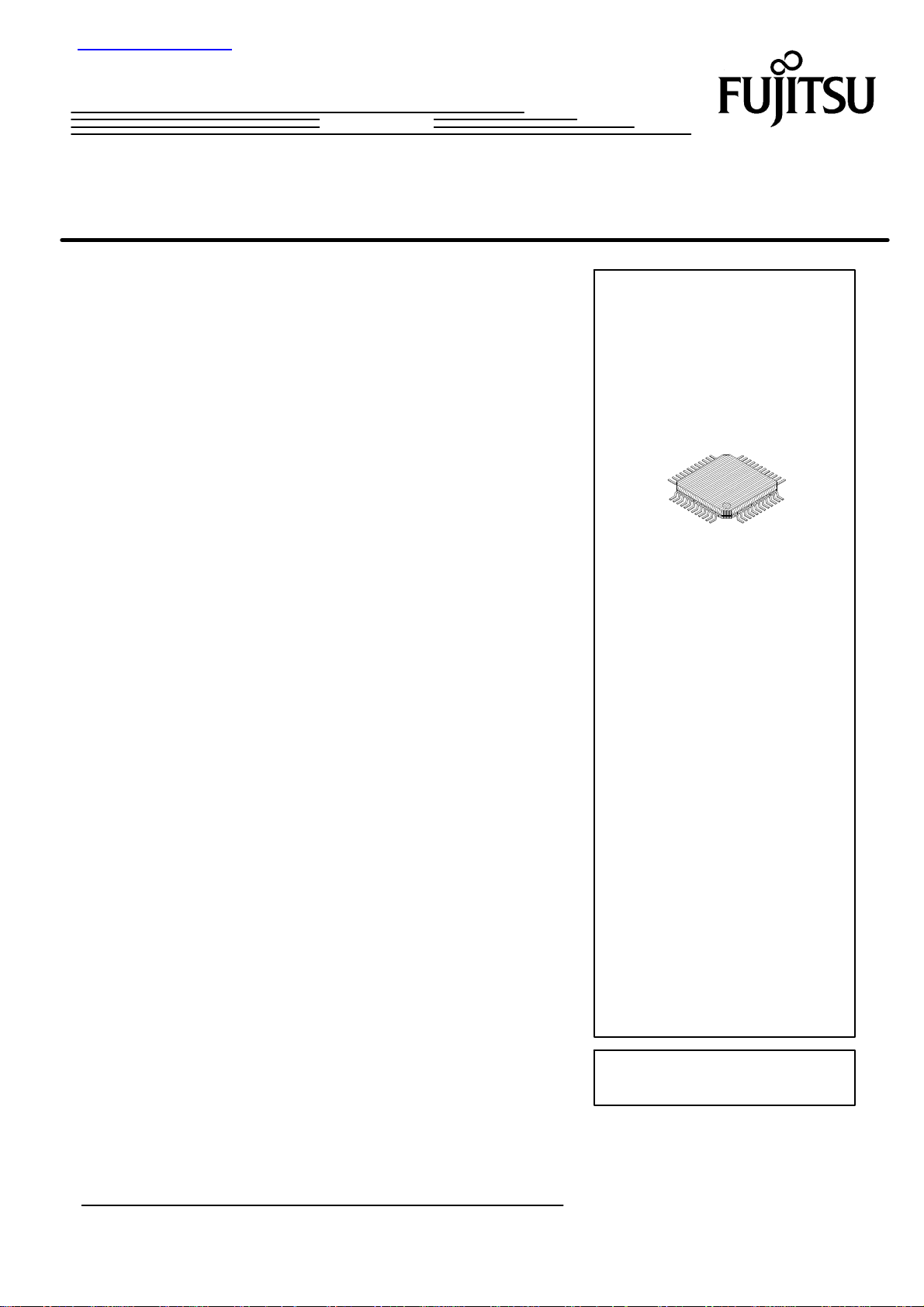
48-PIN PLASTIC LQFP
(FPT-48P-M05)
Copyrightã1998 by FUJITSU LIMITED
This device contains circuitry to protect the inputs against
damage due to high static voltages or electric fields.
However, it is advised that normal precautions be taken to
avoid application of any voltage higher than maximum rated
voltages to this high impedance circuit.
1
Page 2
MB3829
PIN ASSIGNMENT
Voltage monitoring section
Power Controller section
OUT1 : 1
NC : 2
OUT4 : 3
SS : 4
VCC1 : 5
OUT2 : 6
CTL2 : 7
OUT3 : 8
CTL3 : 9
BATT1 : 10
GND2 :11
48 : VCC2
47 : OFF
46 : ON2
45: ON1
44: CT1
(TOP VIEW)
43: CTP
42: CTW
41: RESET
40: CK
39: INH
38: CHOICE
37: SB
Speaker Amp section
36 : IN
35 : BP
34 : FB
33 : GND4
32 : GND3
31 : OUTB
30 : OUTA
29 : VCC4
28 : CLK
27 : IN1
26 : IN2
GND1 :12
CLR : 13
CT2 : 14
CT3 :15
TOUT : 16
(FPT - 48P -M05)
VREF : 17
VCC3 : 18
VCC5 : 19
VO3 : 20
VO2 : 21
VO1 : 22
GND5 : 23
25 : IN3
Sunder section
GND6 : 24
2
Page 3
PIN DESCRIPTION
MB3829
Power supply
control section
10
11
I/O
1
2
3
4
5
6
7
8
9
OUT1
NC
OUT4
SS
VCC1
OUT2
CTL2
OUT3
CTL3
BATT1
GND2
O
-
O
-
-
O
I
O
I
-
-
REG1 output pin (3.0 V)
Unconnected pin (open)
REG4 output pin (3.0 V)
VREF slow- start capacitance connection pin
Power supply pin for power supply control section
REG2 output pin (3.0 V)
REG2 control pin
In REG1 operating
H level: REG2 operation; L level: REG2 OFF
REG3 output pin (3.0 V)
REG3 control pin
In REG1 operating
H level: REG3 operation; L level: REG3 OFF
Backup battery connection pin
Ground pin
DescriptionPin No. Pin Symbol
Sounder section
12
13
14
15
16
17
18
19
20
21
22
23
24
25
GND1
CLR
CT2
CT3
TOUT
VREF
VCC3
VCC5
VO3
VO2
VO1
GND5
GND6
IN3
-
I
-
-
O
O
-
-
O
O
O
-
-
I
Ground pin
Reset pin for momentary power - loss detection and power restoration section
Pin for connecting momentary power - loss evaluation time
setup capacitor
Pin for connecting momentary power - loss evaluation time
setup capacitor and resistor
Pin for momentary power - loss detection and output (open drain)
Pin for reference voltage output
Power supply pin for momentary power - loss detection and
power - restoration section
Power supply pin for sounder section
Output 3 pin (open collector)
Output 2 pin (open collector)
Output 1 pin (open collector)
Ground pin
Ground pin
Control input 3 pin (H level: VO3 operation)
(Continue)
3
Page 4
MB3829
(Continued)
Sounder section
Speaker amplifier
section
26
27
28
29
30
31
32
33
34
35
36
37
38
IN2
IN1
CLK
VCC4
OUTA
OUTB
GND3
GND4
FB
BP
IN
SB
CHOICE
I/O
O
O
DescriptionPin No. Pin Symbol
I
I
I
-
-
-
I
-
I
I
-
Control input 2 pin (H level: Vo2 operation)
Control input 1 pin (H level: Vo1 operation)
Clock input pin
Power supply pin for speaker amplifier section
Output A pin
Output B pin
Ground pin
Ground pin
Inverted input pin
Bypass pin
Non-inverted input pin
Control input pin (H level: speaker amplifier operation)
Earphone selection control pin
Voltage monitoring
section
Power supply
control section
39
40
41
42
43
44
45
46
47
48
INH
CK
RESET
CTW
CTP
CT1
ON1
ON2
OFF
VCC2
I
I
O
-
-
-
I
I
I
-
Inhibit pin
Clock input pin
Reset output pin
Pin for watchdog timer monitoring time setup
Pin for power- on reset hold time setup
Pin for connecting ON time setup capacitor
ON1 pin
ON2 pin
OFF pin
Power supply pin for ON/OFF switch section
4
Page 5

BLOCK DIAGRAM
VCC1
OUT4
3
(3.0V)
5
MB3829
BATTI
(3.18V)
10
1K
VCC3
TOUT
CLR
CT3
1816131514
CT2
VO1
22
VO2
21
VO3
20
OUT3
(3.0V)
CTL3
OUT2
(3.0V)
CTL2
OUT1
(3.0V)
- +
- +
- +
- +
- +
REG1 REG2 REG3 REG4
- +
S
loss detection and
-
Backup section
restoration section
-
power
momentary power
Sound driv-
er
Watchdog
timer
27A
-
MB3793
38 43 41 39 42 40 27 26 25 28 19 23 24
Q
R
Control
Speaker amp.
31
GND1 GND2
+ -
+ -
12 11 1 7 6 9 8
Refernce Voltage
Bias generator
- +
32 33
34 30
ON/OFF switch
29
48
VCC2
44
CT1
45
ON1
46
ON2
47417
SS
OFF
VREF
(1.26V)
37
SB
35
BP
36
IN
VCC4 FB GND3 GND4 OUTAOUTB CHOICE CTP RESET INH CTW CK IN1 IN2 IN3 CLK VCC5 GND5 GND6
5
Page 6

MB3829
Function Descriptions
1. Power supply control section
(1) Reference voltage circuit
The reference voltage circuit generates a temperature- compensated, stable voltage (» 1.26 V). The generated
reference voltage is used as the power supply control section reference voltage or bias.
(2) Series regulator section
A 4- channel series regulator incorporating a low- saturation output transistor is used. All four channels provide an
output voltage of 3.0 V. Their characteristics are described below.
REG1 is suitable for a microcontroller power supply because it is connected to a power-on reset circuit. It is
controlled by the ON/OFF switch section.
ON/OFF control of REG2 and REG3 is exercised independently by the CTL2 and CTL3 pins while REG1 is ON.
REG4 operates at all times and is therefore suitable for data backup.
REGs 1 through 4 incorporate an overcurrent- protection circuit (REG1 to REG3 » -100 mA, REG4 » -25 mA).
(3) Battery backup section
When the main battery is installed, the series regulator recharges a button-type lithium secondary battery, which is
often used to provide backup for clocks and memory. When the main battery is not installed, the backup battery
supplies power to clocks and the battery via a built- in diode. Since the recharging series regulator is set at 3.18 V,
this battery backup section is suitable for manganese and lithium batteries.
(4) ON/OFF switch section
When a time-setup capacitance and resistance are connected to the CT1 pin, the ON1 pin makes it possible to set
the power supply button activation time. This feature prevents turning ON a mobile telephone accidentally.
The ON2 and OFF pins provide a method of exercising direct ON/OFF control of the regulator.
ON time setting calculation formula: T
(5) Momentary power - loss function and power -restoration section
When a time-setup capacitanceand resistance are connected to the CT3 pin, a momentary Vcc loss, which may be
caused by battery replacement, etc., will be detected so as to deliver output to the TOUT pin. At power restoration,
the operating state before the momentary power loss is recovered.
After a momentary power loss, the CLR pin resets the prevailing state so that the momentary power-loss detection
circuit retains the latch circuit state.
Momentary power - loss detection time calculation formula: T
ON
» -C
x RT1x ln (1-1.26V/V
T1
OFF
» -C
)
CC2
x RT3x ln (1-(2.3V - 0.27V)/2.3V)
T3
6
Page 7
(6) ON/OFF setup conditions for individual channels
ON/OFF switching
section
ON2 OFF
CTL2
CTL3 REG1 REG2
REG3ONREG4
MB3829
Battery
backup
L
H
H
L
´
L
H
L
H
´
L
L
H
H
OFF (standby mode)
OFF
ON
ON
OFF
ON
OFF
OFF
ON
ON
ON
2. Speaker amplifier section
A BTL- output type amplifier is used to drive the speaker directly. The typical output power is as high as 90 mW (at
32 W), and the SB pin provides ON/OFF control.
The CHOICE pin controls earphone selection.
3. Sounder section
This section incorporates three low- saturation output transistors for driving the buzzer. IN1, IN2, and IN3 are used
to select the output transistor.
4. Voltage monitoring section
This section incorporates the REG1 output voltage detection functionand watchdog timer function. It outputs a reset
signal to the RESET pin. Further, the detection time varies with the capacitance connected to the CTP and CTW
pins.
7
Page 8
MB3829
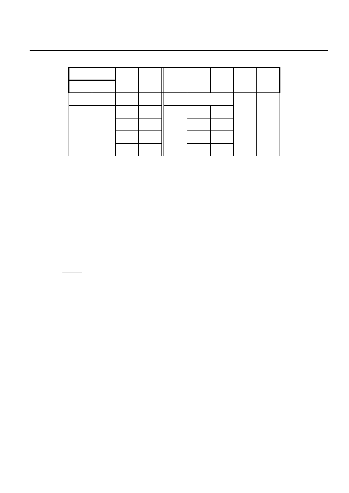
ABSOLUTE MAXIMUM RATINGS
Parameter Symbol
Power-supply voltage
Common to all
sections
Power supply control
section
Speaker amplifier
section
Sounder section
Voltage monitoring
section
*: Value as mounted on double-sided epoxy board 10 ´ 10 cm
NOTE: Permanent device damage may occur if the above Absolute Maximum Ratings are exceeded. Functional operation should be
restricted to the conditions as detailed inthe operationalsections ofthis datasheet. Exposure to absolute maximumrating conditions
for extended periods may affect device reliability.
Power dissipation
Storage temperature
Output current
Output current
Output current
Reset output current
V
CC
P
Tstg
IO1to I
I
O4
I
O
I
O1
I
O2
I
O3
IOL, I
D
O3
OH
Condition
—
TA£ +25°C
—
—
Duty = 50%
Duty = 50%
Duty = 50%
DC
Value
10
860*
-50 to +125
-60
-12
150
240
120
60
-10 to 10
Unit
V
mW
°C
mA
mA
mA
mA
mA
mA
mA
RECOMMENDED OPERATING CONDITIONS(1)
Common
to all sections
Parameter Symbol
Power supply voltage
Power supply voltage buildup time
Operation temperrature
V
TV
CC
CC
T
A
Condition
—
—
—
Min.
3.49
50
-30
Value
Typ.
—
—
25
Max.
8.0
—
85
Unit
V
mS/V
°C
8
Page 9

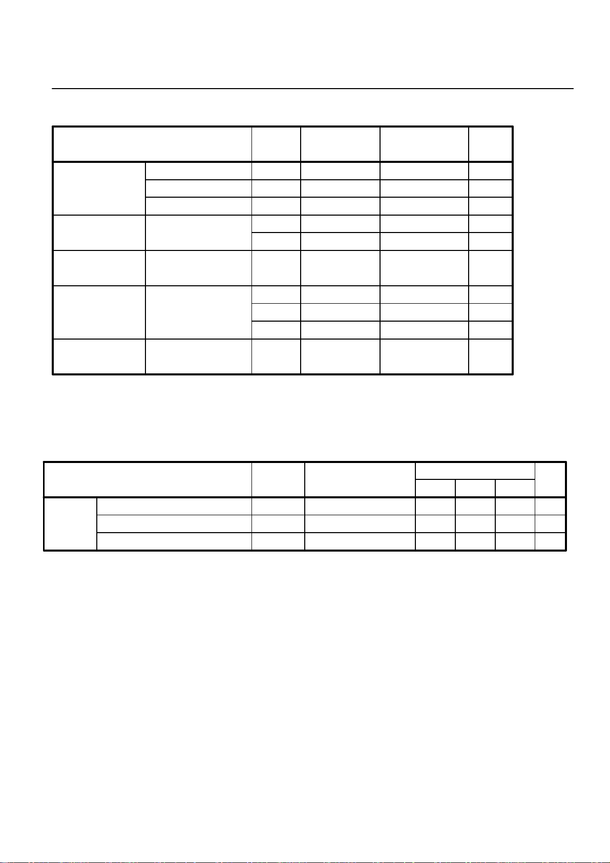
RECOMMENDED OPERATING CONDITIONS(2)
MB3829
Power
supply
control
section
Speaker
amplifier
section
Sounder
section
Voltage
monitoring
section
Parameter Symbol
Control input voltage
Output current
Backup current
CLR input pulse width
OFF input pulse width
ON2 input pulse width
ON setting
Capacitance
time setup
Resistance
Momentary
power-loss
time setup
Capacitance
Resistance
Control input voltage
Amplifier input voltage
Load resistance
Gain setting range
Control input voltage
Output current
RESET output current
Reset/hold time setup capacitance
Clock monitoring time setup
capacitance
Clock monitoring time setting
V
IO1to I
I
O4
I
BATT1
T
CLR
T
OFF
T
ON2
C
T1
R
T1
C
T3
R
T3
V
V
R
AV
V
I
O1
I
O2
I
O3
IOL, I
C
TP
C
TW
T
WD
Condition
I
O3
CT3 = 2.2 mF, RT3 = 1MW
I
IN
L
When Non- INV input
When INV input
I
Duty = 50%
Duty = 50%
Duty = 50%
OH
—
—
—
—
—
—
—
—
—
—
—
—
—
—
—
—
—
—
Value
Min. Max.Typ.
0
-50
-10
—
200
10
10
—
1.5
—
—
2.2
—
0
0.3
8
6
-26
-20
0
—
—
—
-3
0.001
0.001
0.1
—
—
—
—
—
—
—
—
—
32
24
—
—
—
—
—
—
—
—
Unit
V
CC
—
—
200
—
—
—
—
1
—
—
1
—
V
CC
VCC-0.8
200
36
36
V
CC
200
100
50
3
10
1
1500
V
mA
mA
mA
ns
ms
ms
mF
MW
mF
MW
V
V
W
dB
dB
V
mA
mA
mA
mA
mF
mF
ms
Note: The recommended operating conditions are the recommended values guaranteeing normal LSI operations. The specified
values for electrical characteristics are guaranteed when the conditions in the ”Condition” column, as well as the recommended
operating conditions, are met.
9
Page 10

MB3829
ELECTRICAL CHARACTERISTICS
1. Power supply control section
Parameter Symbol
Reference
voltage
section
Reference voltage
V
REF
IO=0mA
Condition
(V
CC1,2,3
Value
Min. Max.Typ.
1.23
1.26
= +3.6V, TA= +25°C)
Unit
1.29
V
Constant
Voltage
Controller
(REG1)
Constant
Voltage
Controller
(REG2,3)
Output voltage
Output saturation voltage
Temperature regulation of
output voltage
Input stability
Load stability
Ripple removal ratio
Rise time
Output voltage
Output saturation voltage
Temperature regulation of
output voltage
Input stability
Load stability
Ripple removal ratio
Input- on condition
Input- off condition
Input current
Rise time
V
O
V
O
V
SAT
D VO/V
Line
Load
R.R
T
R
V
O
V
O
V
SAT
D VO/V
Line
Load
R.R
V
ON
V
OFF
I
IH
I
IL
T
R
IO=0mA
IO=-50mA
IO=-22mA, VCC=3V
TA=-30 to +85 °C
O
VCC=3.49V to 8V,IO=-10mA
IO=0mA to - 50mA
VIN=0.2Vrms,
IO=-10mA
C=10mF, R=60W
IO=0mA
IO=-50mA
IO=-40mA, VCC=3V
TA=-30 to +85 °C
O
VCC=3.49V to 8V,IO=-10mA
IO=0mA to - 50mA
VIN=0.2Vrms,
IO=-10mA
-
-
VI=3.0V
VI=0.4V
C=10mF, R=60W
f=25Hz
f=1kHz
f=25Hz
f=1kHz
2.90
2.90
—
*
—
—
—
*
38
*
23
*
—
2.90
2.90
—
*
—
—
—
*
38
*
23
2.0
0
—
1
*
—
3.00
3.00
0.15
1
10
10
50
35
250
3.00
3.00
0.25
1
10
10
50
35
—
—
17
2
250
3.13
3.13
0.27
2
50
50
—
—
410
3.13
3.13
0.45
2
50
50
—
—
V
CC
0.8
30
3
410
V
V
V
%
mV
mV
dB
dB
ms
V
V
V
%
mV
mV
dB
dB
V
V
mA
mA
ms
*: Guaranteed by design
10
Page 11

MB3829
Parameter Symbol
Constant
Output voltage
Voltage
Controller
(REG4)
Output saturation voltage
Temperature regulation of
output voltage
Input stability
Load stability
Ripple removal ratio
Output leakage current
Rise time
Backup
Section
Output voltage
Charging current
Output saturation voltage
Output leakage current
Input- on condition
ON/OFF
switch
Input- off condition
section
Input current
Threshold voltage
CT3 output resistance
ON setup time
*: Guaranteed by design
V
O
V
O
V
SAT
D VO/V
Line
Load
R.R
I
LEAK
T
R
V
BATT1
I
BATT1
D V
I
LEAK
V
ON
V
OFF
I
IH
I
IL
V
TH
R
ON
T
ON
Condition
IO=0mA
IO=-10mA
IO=-2mA, VCC=3V
TA=-30 to +85 °C
O
VCC=3.49V to 8V
IO=0mA to - 10mA
VIN=0.2Vrms,
IO=-2mA
V
=0 to 2.97V,
CC1
V
=0V, VO4=3V
BATT1
C=10mF, R=300W, SS=1nF
I
=0mA
BATT1
V
=2.0V
BATT1
V
O
=0V, IO4=-20mA
CC1
V
=0 to 2.97V,
CC1
V
=3V, VO4: Short-
BATT1
circuited to V
-
-
VI=3.0V
VI=0.4V
CT1 pin
OFF=H
CT1=1.5mF, RT1=1MW
BATT1
f=25Hz
f=1kHz
Min. Max.Typ.
2.90
2.90
—
*
—
—
—
*
38
*
4
—
*
—
3.10
—
0.52
—
2.0
0
—
1
*
1.21
0.5
550
(V
CC1,2,3
Value
3.00
3.00
0.05
1
10
10
50
16
1.2
900
3.18
-1.18
0.57
2.1
—
—
17
2
1.26
1
650
= +3.6V, TA= +25°C)
Unit
3.13
3.13
0.1
2
50
50
—
—
10
1450
3.25
-0.59
0.62
10
V
CC
0.8
30
3
1.31
1.5
750
V
V
%
mV
mV
dB
dB
V
mA
ms
V
mA
V
mA
V
V
mA
mA
V
kW
ms
11
Page 12

MB3829
Instantaneous
Detection/
Power
Restoration
Section
Power
supply
control
section
Parameter Symbol
Detection voltage
Instantaneous detection time
Input- on condition
Input- off condition
Input current
Output leakage current
Output saturation voltage
Stand-bycurrent
Power-off current
Power-oncurrent
Power-oncurrent
Power-oncurrent
V
THL
T
OFF
V
V
OFF
I
I
I
LEAK
V
SAT
I
CC1
I
CC2
I
CC3
I
CC4
I
CC5
CT3=2.2mF, RT3=1MW
CLR pin
ON
CLR pin
VI=3.0V
IH
VI=0.4V
IL
V
CC1,2,3
IO=100mA
REG1 to REG3 : OFF
IO4=-100mA
I
=-200mA
BATT1
REG2,3 : OFF
IO1=-11mA, IO4=-100mA
I
=-200mA
BATT1
REG3 : OFF
IO1=-11mA, IO2=-30mA
IO4=-100mA
I
=-200mA
BATT1
IO1=-11mA, IO2=-40mA
IO3=-12mA, IO4=-100mA
I
=-200mA
BATT1
IO1to IO4, I
Condition
VCCpin
= VO=8V
BATT1
: No load
(V
CC1,2,3
Value
Min. Max.Typ.
1.90
4.0
2.0
0
—
1
—
—
2.2
4.7
—
—
17
2
—
0.1
— 9060
— 240160
— 280190
— 530360
— 240160
= +3.6V, TA= +25°C)
Unit
V
s
V
V
mA
mA
mA
V
V
2.5
5.5
CC
0.8
30
3
10
0.3
mA
mA
mA
mA
mA
Note: The Icc1to Icc5values forthe whole powersupply control sectionrepresent the sum ofVcc1 to Vcc3 pincurrent values except the load
current.
12
Page 13

2. Speaker amplifier section
Parameter Symbol
Speaker
amplifier
section
Earphone
Input impedance
Input- ON condition
Input- OFF condition
Input current
Power-supply current at standby
Power-supply current at no load
(Speaker mode)
Voltage gain
Release voltage gain
Output power
Output voltage
Offset voltage between output
Distortion rate of all high frequencies
Ripple extraction ratio
Rise time
Voltage gain
Output voltage
Rise time
A
V
A
VO
P
D
V
O
V
OO
THD
PSRR
T
R
A
VI
V
OI
T
R
R
IN
V
ON
V
OFF
I
IH
I
IL
I
CC1
I
CC2
Condition
Non-INV input
f £ 100 Hz
RL= 32 W, THD = 10 %
No load
-
PO³ 25 mW
-
PO³ 25 mW, BP=4.7mF
-
No load
PO³ 6 mW, BP=4.7mF
-
-
-
VSB=3.0V
VSB=0.4V
-
When no signal
Min. Max.Typ.
*
3.8
-50
*
*
1.4
*
*
2.0
22
—
60
—
33
—
16
—
20
—
—
—
—
MB3829
(V
Value
5.5
0.5
2.75
0
= +3.6V, TA= +25°C)
CC1,2,3
24
80
90
—
45
—
18
—
30
—
—
17
0
0
3
26
—
—
—
50
1.0
—
0.25
20
—
0.25
50
V
CC
0.8
30
1
10
5
Unit
dB
dB
mW
V
mV
%
dB
s
dB
V
s
kW
V
V
mA
mA
mA
mA
Power-supply current at no load
(Earphone mode)
Speaker ON condition
Earphone ON condition
*: Guaranteed by design
I
CC3
VSON
VEON
When no signal
-
-
—
2.0
V
2.5
0.8
CC
mA
V
V
1.5
0
—
—
13
Page 14

MB3829
3. Sounder
Parameter Symbol
Output voltage
Output leakage current
Input- ON condition
Input- OFF condition
Input current
Power-supply current at standby
Power-supply current at no load
V
V
V
I
LEAK
V
V
OFF
I
I
I
CC1
I
CC2
I
CC3
I
CC4
O1
O2
O3
ON
IH
IL
Condition
IO1= 200 mA
IO2= 100 mA
IO3= 50 mA
V
CC1,2,3=VO
= 8 V
-
-
VI= 3.3 V
VI= 0.4 V
-
V
= 3.0 V, CLK Duty = 50%
IN1
V
= 3.0 V, CLK Duty = 50%
IN2
V
= 3.0 V, CLK Duty = 50%
IN3
Min.
—
—
—
—
2.0
0
—
2
—
—
—
—
(V
= +3.6V, TA= +25°C)
CC5
Value
Typ.
0.3
0.3
0.3
—
—
—
34
4
2
3.0
1.5
0.8
Max.
0.5
0.5
0.5
10
V
CC
0.8
60
6
10
4.5
2.3
1.2
Unit
V
V
V
mA
V
V
mA
mA
mA
mA
mA
mA
14
Page 15

4. Voltage monitoring section
Parameter Symbol
V
V
V
V
V
V
V
V
V
t
t
tr*1
tr*1
T
V
SL
SH
SHYS
CIH
CIL
CHYS
IIH
V
IIL
I
INH
I
INL
OH
OL
CCL
t
PR
t
WD
t
WR
CKW
CKT
PD
T
PI
Detection voltage OUT1 fall
Detection voltage hysteresis width
CK input threshold voltage
CK input hysteresis width
Inhibit input voltage
Input current
CK
IHB
Reset output voltage
Reset output minimum voltage
Power-on reset hold time
Watchdog timer monitoring time
Watchdog timer reset time
Clock input pulse width
Clock input pulse cycle
RESET rise time
RESET fall time
Delay time from OUT1
OUT1 input pulse width
*1: The voltage range prevailing during RESET output rise/fall time measurement is from 10% to 90%
*: Guaranteed by design
Condition
OUT1 rise
VSH- V
SL
-
-
-
-
-
VIN= OUT1
VIN= GND
I
= - 3mA
RESET
I
= +3mA
RESET
I
= +50mA
RESET
CTP= 0.1mF
CTW=0.01mF, CTP=0.1mF
CTP= 0.1mF
-
-
CL= 50pF
CL= 50pF
-
1.2V to 2.5V
*
*
*
*
*
*
(OUT1 = +3.0V, TA= +25°C)
Value
Min.
2.70
2.76
35
0.6
0.4
0.1
1.8
—
—
-1.0
2.5
—
—
25
8
1.5
500
20
2.0
—
—
16
Typ.
2.75
2.81
65
1.2
0.9
0.3
—
—
0
0
2.8
0.12
0.8
70
16
5
—
—
—
—
2
—
Max.
2.81
2.87
95
1.8
1.4
0.6
—
0.8
1.0
—
—
0.4
1.2
115
24
8.5
—
—
500
500
20
—
MB3829
Unit
V
V
mV
V
V
V
V
V
mA
mA
V
V
V
ms
ms
ms
ns
ms
ns
ns
ms
ms
15
Page 16

MB3829
TYPICAL CHARACTERISTICS CURVE
Allowable dissipation vs. ambient temperature curve
1000
800
[mW]
D
Allowable dissipation P
LQFP
600
400
200
0
-40 -20 0 20 40 60 80 100
Ambient temperature TA[°C]
16
Page 17

VOLTAGE MONITORING SECTION TIMING CHART
V
SH
V
OUT1
CK
INH
CTP
SL
V
CCL
t
CKW
MB3829
CTW
RESET
V
H
V
L
t
PR
(1) (2) (3) (4) (5) (6) (7) (8) (9) (10) (11) (12) (13) (14)
t
WD
t
WR
t
PR
17
Page 18

MB3829
DESCRIPTION OF OPERATION
(The numbers in the timing diagram correlate to the numbers (1) to (13) below.)
(1) When the REG1 output voltage (OUT1) is about 0.8 V (V
(2) When OUT1 reaches a level higher than the detection voltage (VSH), the power-on reset/hold time setup ca-
pacitor (CTP) begins to charge. The VSHvalue is 2.81 V.
(3) When the power- on reset/hold time setup pin (CTP) voltage rises above the threshold level (Vth), the reset
clears (RESET pin voltage changes from L level to H level). The Vth value is about 1.9 V.
The power- on reset/hold time (tPR) is expressed by the following equation.
Also, the watchdog timer monitoring time setup capacitor (CTW) begins to charge.
t
[ms] » A x C
PR
A » 700
(4) When the watchdog timer monitoring time setup pin (CTW) voltage reaches the Hi level (VH), the CTWchanges
from the charged state to the discharged state. The VHvalue is about the reference voltage of 1.24 V.
(5) When a clock pulse input is applied to the clock pin (CK) and then the next clock pulse input is applied (positive
edge trigger) to the CK pin during a CTWdischarge, switching from the discharged state to the charged state
occurs.
(6) If a clock pulse input is not delivered to the clock pin (CK) within the watchdog timer monitoring time (tWD), the
CTW pin voltage falls below the Lo level (VL) so the reset signal is output (RESET pin voltage changes from H
level to the L level).
The VLvalue is about 0.24 V.
The watchdog timer monitoring time (tWD) is expressed by the following equation.
), the reset signal is output.
CCL
[mF]
TP
t
[ms] » B x C
WD
B » 1600
(7) When the CTPis recharged to raise the CTPpin voltage above Vth, the reset clears, allowing the watchdog timer
to start running.
The watchdog timer monitoring reset time (tWR) is expressed by the following equation.
t
[ms] » D x C
WR
B » 50
(8) When the OUT1 drops below the fall period detection voltage (VSL), the CTPpin voltage falls so that the reset
signal is output (RESET pin voltage changes from H level to the L level).
The VSLvalue is about 2.75 V.
(9) When the OUT1 rises above VSH, CTPcharging starts.
(10) When the CTPpin voltage rises above Vth, the reset clears, causing the watchdog timer to start running.
(11) When the inhibit signal is input (Hi level), the watchdog timer operation is forcibly stopped.
In this case, only the watchdog timer stops and the OUT1 monitoring operations ((8) to (10)) are performed. If
the inhibit input does not clear, the watchdog timer does not operate.
(12) When the inhibit input clears (becomes Lo level), the watchdog timer begins to operate.
(13) When the REG1 output turns OFF and OUT1 falls below VSL, the reset signal is output.
TW
TP
[mF]
[mF]
18
Page 19

REG SECTION RISE TIMING REQUIREMENTS
VCC
ON2
CTL2
CTL3
T
R
MB3829
REG1
REG2
REG3
REG4
T
R
90%
90%
T
R
90%
T
R
90%
SPEAKER AMPLIFIER SECTION RISE TIMING REQUIREMENTS
VCC4=VSB CHOICE=”L” (BP=4.7mF)
Speaker output = 25mW
Speaker output
T
VCC4=VSB =CHOICE (BP=4.7mF)
Earphone output = 6mW
Earphone output
0V
T
R
R
19
Page 20

MB3829
APPLICATION CIRCUIT
Memory
Receiver
Transmitter
Microcontroller
3.6V
5
VCC1
3
OUT4
BATTI
(3.0V)
OUT1
Backup battery
10
(3.18V)
3.6V
Momentary power-loss detection signal
100kW
18
VCC3
1MW
(to microcontroller)
2.2mF
From
microcontroller
161315
CT3
CLR
TOUT
14
CT2
20pF
VCC5
Buzzer
15mF 1kW
10W
50W
150W
22
21
20
VO1
VO2
VO3
3.6V
28 19 23 24
Control
signal
Control
signal
Sounder section
Control
Control
signal
Control
signal
3.6V
signal
From
microcontroller
15kW
2.2kW
on reset signal
-
(to microcontroller)
Power
1mF
27 26 25
40
42
9 8
6
Voltage control section
7
1
12 11
GND1 GND2 OUT1 CTL2 OUT2 CTL3 OUT3
CT1
ON1
VCC2
48
44
ON2
454647
OFF
MB3829
SS
VREF
(1.26V)
4
17
section
Voltage monitoring
Speaker amplifier section
SB
BP
37
35
39
43 41
31
32 33 38
34 30
29
IN
VCC4 FB GND3 GND4 OUTA OUTB CHOICE CTP RESET INH CTW CK IN1 IN2 IN3 CLK VCC5 GND5 GND6
36
20
VCC2
(3.6V)
3.6V
1.5mF
Control
1M W
signal
Control
signal
10mF
0.1mF
Page 21

MB3829
USAGE PRECAUTIONS
1. Device settings must not exceed the maximum ratings.
Usage under conditions exceeding absolute maximum ratings may permanently damage LSI devices.
Note also that in normal operation usage within recommended operating conditions is preferred, and that the
reliability of LSI devices may be adversely affected when used outside these conditions.
2. Devices should be used within recommended operating conditions.
Recommended operating conditions are recommended values within which the LSI device is warranted to operate
normally.
Rated values of electrical characteristics are warranted within the range of recommended operating conditions and
within the conditions listed in the condition column for each parameter.
3. The PC board ground line must be designed by taking the common impedance.
4. Guard against static electricity.
The semiconductor containers must be protected against static electricity or made of conductive materials.
When storing or transporting a component - mounted PC board, place it in a conductive bag or container.
Ensure that the workbenches, tools, and measuring instruments are grounded.
Workers must be grounded via a series resistance of 250 kW to 1 MW.
ORDERING INFORMATION
Part number Package Remarks
MB3829PFV- G - BND Plastic, LQFP, 48- pin
(FPT - 48P -M05)
21
Page 22

MB3829
PACKAGE DIMENSIONS
48-LEAD PLASTIC FLAT PACKAGE
(CASE No.: FPT-48P-M05)
37
48
LEAD No.
.0197±.0031
(0.50±0.08)
.354±.008
(9.00±0.20)
.276±.004
36
1
(7.00±0.10)
INDEX
SQ
SQ
.007
(0.18 )
.004(0.10)
25
+.003
-.001
+0.08
-0.03
+.008
.059
-.004
+0.20
(1.50 )
-0.10
24
.217(5.50)
REF
13
12
”A”
.005
(0.127 )
Details of “A” part
.004±.004
(0.10±0.10)
.020±.008
(0.50±0.20)
0°to10°
(MOUNTING HEIGHT)
.315(8.00)
NOM
+.002
-.001
+0.05
-0.02
(STAND OFF
HEIGHT)
ã1991 FUJITSU LIMITED F48013S-2C
Dimensions in
inches (millimeters)
22
Page 23

MEMO
MB3829
All Rights Reserved.
Circuit diagrams utilizing Fujitsu products are included as a means of illustrating
typical semiconductor applications. Complete information sufficient for construction purposes is not necessarily given.
The information contained in this document has been carefully checked and is
believed to be reliable. However, Fujitsu assumes no responsibility for inaccuracies.
The information contained in this document does not convey any license under the
copyrights, patent rights or trademarks claimed and owned by Fujitsu.
Fujitsu reserves the right to change products or specifications without notice.
No part of this publication may be copied or reproduced in any form or by any
means, or transferred to any third party without prior written consent of Fujitsu.
23
Page 24

MB3829
For further information please contact:
Japan
FUJITSU LIMITED
Corparate Grobal Business Support Div.,
Electronic Devices
4- 1 -1 Kamikodanaka, Nakahara -ku, Kawasaki -shi,
Kanagawa- ken 211-8588, Japan
Tel: (044) 754 -3763
FAX: (044) 754 - 3329
North and South America
FUJITSU MICROELECTRONICS, INC.
Integrated Circuits Division
3545 North First Street
San Jose, CA 95134-1804, USA
Tel: (408) 922 -9000
FAX:(408) 922- 9179
Europe
FUJITSU MIKROELEKTRONIK GmbH
Am Siebenstein 6-10,
63303 Dreieich-Buchschlag,
Germany
Tel: (06103) 690-0
FAX: (06103) 690-122
Asia
FUJITSU MICROELECTRONICS ASIA PTE LIMITED
#05- 08, 151 Lorong Chuan
New Tech Park
Singapore 556741
Tel: (65) 281 -0770
FAX: (65) 281- 0220
ã FUJITSU LIMITED 1998
24
 Loading...