

Page 1
FUJITSU SEMICONDUCTOR
DATA SHEET
ASSP
SWITCHING REGULATOR
CONTROLLER
MB3788
DESCRIPTION
■■■■
The MB3788 is a dual-channel PWM-type switching regulator controller; it incorporates a reference voltage.
The MB3788 has a PWM circuit and an output circuit as well as a reference v o ltage po w er supply with a voltage
accuracy of ±1%. The maximum operating frequency is 1 MHz. It is designed f or a voltage-drop output s witching
regulator suitable for a logic power supply or speed control of a DC motor.
The MB3788 is compatible with all master ICs producing triangular wav es, sa w-tooth w a v es and sine wa v es with
an amplitude of 1.3 V to 1.9 V.
It can be used in high-performance portable equipment such as a video camcorder or notebook personal computer
(word processor).
DS04-27209-3E
FEATURES
■■■■
• Wide operating power supply voltage range: 3.6 V to 18 V
• Low power dissipation
• Operating: 1.9 mA (standard)
Standby: 10 µA Max
(Continued)
PACKAGE
■■■■
24-pin Plastic SSOP
(FPT-24P-M03)
This device contains circuitry to protect the inputs against damage due to high static voltages or electric fields. Howe ver, it is
advised that normal precautions be taken to avoid application of any v oltage higher than maxim um rated v oltages to this high
impedance circuit.
Page 2

MB3788
(Continued)
• High-frequency operation: 100 kHz to 1 MHz
• On-chip timer and latch-type short-circuit detection circuit
• Wide error amplifier input voltage range: -0.2 V to V
• On-chip high-accuracy reference voltage circuit: 2.50 V ±1%
• Output circuit
PNP transistor drive output pin: Push-pull type
ON/OFF current values set independently
• On-chip standby function and output control function
• High-density packaging: SSOP-24P
PIN ASSIGNMENT
■■■■
(TOP VIEW)
CC(out)
V
OUT1
VE1
Cb1
Ca1
FB1
-IN1(E)
+IN1(E)
-IN1(C)
-IN(PWN)
V
CC
VREF
1
2
3
4
5
6
7
8
9
10
11
12
CC
- 1.8 V
24
23
22
21
20
19
18
17
16
15
14
13
GND
OUT2
VE2
Cb2
Ca2
FB2
-IN2(E)
+IN2(E)
-IN2(C)
SCP
CTL2
CTL1
(FPT-24P-M03)
2
Page 3
PIN DESCRIPTION
■■■■
Pin No. Pin name I/O Descriptions
MB3788
Channel 1
Channel 2
2OUT1O
3VE1I
4Ca1—
5Cb1—
6FB1O
7-IN1(E)I
8+IN1(E)
9-IN1(C)I
16 -IN2(C) I
17 +IN2(E) I
18 -IN2(E) I
19 FB2 O
20 Ca2 —
21 Cb2 —
22 VE2 I
23 OUT2 O
13 CTL1 I
Channel 1 push-pull type output
Channel 1 output current setting
Channel 1 output transistor OFF current setting: Output transistor OFF
The current is set by connecting a capacitor between pins Ca1 and Cb1.
Channel 1 error amplifier output
Channel 1 error amplifier inversion input
Channel 1 error amplifier non-inversion input
Channel 1 comparator inversion input
Channel 2 comparator inversion input
Channel 2 error amplifier non-inversion input
Channel 2 error amplifier inversion input
Channel 2 error amplifier output
Channel 2 output transistor OFF current setting: Output transistor OFF
The current is set by connecting a capacitor between pins Ca2 and Cb2.
Channel 2 output current setting
Channel 2 push-pull type output
Power and channel 1 control pin
H level: Power and channel 1 operating
L level: Standby
Control
circuit
Power
circuit
14 CTL2 I
15 SCP —
1
2
V
CC
10 -IN(PWM) I
11 VCC1 —
12 VREF O
24 GND —
Channel 2 control pin
When CTL1 pin = H level,
H level: Channel 2 operating
L level: Channel 2 OFF
Short-circuit protection circuit capacitor connection
Output circuit power pin
—
Master oscillating waveform input
Reference power and control circuit power
Reference voltage output
Ground
Note: The alphabetic characters in parenthesis above indicate the following input pins.
(C): Comparator
(E): Error amplifier
3
Page 4
MB3788
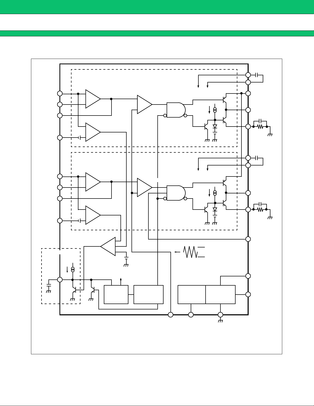
BLOCK DIAGRAM
■■■■
+IN1 (E)
-IN1 (E)
-IN1 (C)
+IN2 (E)
-IN2 (E)
-IN2 (C)
FB1
FB2
8
7
6
9
17
18
19
16
0.6 V
0.6 V
Channel 1
Error amplifier 1
+
-
Comparator 1
+
-
Channel 2
Error amplifier 2
+
-
Comparator 2
+
-
PWM comparator 1
+
-
PWM comparator 2
+
-
OFF current setting
OFF current setting
1.5 V
1.5 V
20
21
23
22
4
5
1
2
3
Cb1
Ca1
CC(out)
V
OUT1
VE1
Ca2
Cb2
OUT2
VE2
Timer circuit
SCP
15
1 µA
SCP comparator
-
-
+
SR latch
circuit
VREF
2.1 V
Low input
voltage
protection
circuit
10 12
-IN(PWM)
Reference
voltage
power (2.5 V)
V
REF
1.9 V
1.3 V
Power/channel
ON/OFF
circuit
24
GND
CTL2
14
CC
V
11
CTL1
13
4
Page 5

MB3788
FUNCTIONAL DESCRIPTION
■■■■
1. Major Functions
(1) Reference voltage power circuit
The reference voltage po wer supply produces a reference v oltage (≈ 2.50 V) which is temperature-compensated
by the voltage supplied from the power pin (pin 11); it is used as the IC internal circuit operating power supply.
The reference voltage can also be output externally at 1 mA from V
(2) Error amplifier
The error amplifier detects the switching regulator output voltage and outputs a PWM control signal. It has a
wide in-phase input voltage range of -0.2 V to V
Connecting the output pin and inversion input pin of the error amplifier through a f eedback resistor and capacitor
allows setting of any loop gain to provide stable phase compensation.
(3) PWM comparator
The PWM comparator controls the output pulse ON time according to the input voltage.
The voltage input to the -IN pin (PWM) turns the output transistor on when it is lower than the output v oltage of
the error amplifier.
(4) Output circuit
CC
- 1.8 V to make setting from an external power supply easy.
REF
pin (pin12).
The output circuit is configured in a push-pull form and uses a PNP transistor drive system to drive a transistor
of up to 30 mA. (See
How to Set Output Current.
)
2. Channel Control Function
Channels can be set ON/OFF by combining the voltage levels at pin CTL1 (pin 13) and pin CTL2 (pin 14).
Channel ON/OFF Setting Conditions
Voltage level at CTL pin Channel ON/OFF status
CTL1 CTL2 Power circuit Channel 1 Channel
L × Stand by state*
HH
ON
LOFF
*: The power current in the standby state is 10 µA Max.
ON
5
Page 6

MB3788
3. Protection Functions
(1) Timer and latch-type short-circuit protection circuit
The SCP comparator detects the output voltage levels of two comparators to detect an output short circuit. If
the output voltage of one comparator increases to 2.1 V, the transistor of the timer circuit is turned off and the
short circuit protection capacitor connected externally to the SCP pin (pin 15) starts charging.
The latch circuit turns off the output transistor and simultaneously clears the duty cycle to 0 when the output
voltage lev el of the comparator does not return to the normal voltage lev el until the capacitor v oltage rises to the
base-emitter junction voltage VBE (≈ 0.65 V) of the transistor . (See
Type Short-Circuit Protection Circuit.
When the protection circuit operates, recycle the power to reset the circuit.
(2) Low input voltage malfunction fail-safe circ uit
A transient at power-on, or an instantaneous supply v oltage drop can cause a control IC malfunction, which may
damage the system. The low input voltage malfunction fail-safe circuit detects the internal reference voltage
level based on the supply voltage level, resets the latch circuit, turns off the output transistor, clears the duty
cycle to 0 and holds the SCP pin (pin 15) at Low level. All circuits are recovered when the supply voltage is
greater than the threshold voltage of the fail-safe circuit.
)
How to Set Time Constant for Timer & Latch-
6
Page 7
■ ABSOLUTE MAXIMUM RATINGS
MB3788
A
= +25°C)
(T
Parameter Symbol Conditions
Unit
Min Max
Ratings
Supply voltage V
Control input voltage V
Allowable loss P
Operating ambient temperature T
Storage temperature T
CC
ICTL
D
OP
stg
——
——
Ta ≤ +25°C
—
—
—
-30 +85 °C
-55 +125 °C
20 V
20 V
500* mW
*: Value obtained when mounted on 4 cm × 4 cm double-sided epoxy substrate
WARNING: Semiconductor devices can be permanently damaged by application of stress (voltage, current,
temperature, etc.) in excess of absolute maximum ratings. Do not exceed these ratings.
■ RECOMMENDED OPERATING CONDITIONS
A
(T
= +25°C)
Parameter Symbol Conditions
Supply voltage V
Reference voltage output current I
CC
OR
Min Typ Max
—3.66.018V
—-1—0mA
Values
Unit
Error amplifier input voltage V
Error amplifier input voltage V
Control input voltage V
Output current I
Operating frequency f
Operating ambient temperature T
I
I
ICTL
O
osc
op
—-0.2—V
—-0.2—VCCV
—-0.2—18V
—3.0—30mA
— 100 300 1000 kHz
— -30 25 85 °C
CC
- 1.8 V
WARNING: The recommended operating conditions are required in order to ensure the normal operation of the
semiconductor device. All of the device’s electrical characteristics are warranted when the device is
operated within these ranges.
Always use semiconductor devices within their recommended operating condition ranges. Operation
outside these ranges may adversely affect reliability and could result in device failure.
No warranty is made with respect to uses, operating conditions, or combinations not represented on
the data sheet. Users considering application outside the listed conditions are advised to contact their
FUJITSU representatives beforehand.
7
Page 8

MB3788
ELECTICAL CHARACTERISTICS
■■■■
(VCC =6V, TA = +25°C)
Reference
voltage
Low voltage
malfunction
fail-safe
circuit
Short-circuit
detection
comparator
Short-circuit
detector
Parameter Symbol Conditions
∆V
V
OS
V
V
IB
REF
REF
REF
tH
tL
HYS
R
IO
ICM
tPC
STB
I
OR
I
= -1 mA
/
TA = -30° to +85°C-2±0.2 2 %
CC
= 3.6 V to 18 V — 2 10 mV
OR
= -0.1 mA to 1 mA — 3 10 mV
REF
V
= 2 V -20 -8 -3 mA
VI = 0 V -200 -100 — nA
Reference voltage V
Output voltage temperature
variation
Input stability Line V
Load stability Load I
Short-circuit output current I
Threshold voltage
Hysteresis width V
Reset voltage V
Input offset voltage V
Input bias current I
In-phase input voltage range V
Threshold voltage V
Input standby voltage V
Input latch voltage V
Value
Unit
Min Typ Max
2.475 2.500 2.525 V
——2.65—V
——2.45—V
—80200—mV
—1.51.9—V
— 0.58 0.65 0.72 V
—-0.2—V
— 0.60 0.65 0.70 V
— — 50 100 mV
— — 50 100 mV
CC
-1.8 V
Error
amplifier
Input source current I
Input offset voltage V
Input offset current I
Input bias current I
In-phase input voltage range V
Voltage gain A
Ibpc
IO
IO
IB
ICM
V
— -1.4 -1.0 -0.6 µA
VFB = 1.6 V -10 — 10 mV
VFB = 1.6 V -100 — 100 nA
VFB = 1.6 V -200 -60 — nA
—-0.2—V
CC
-1.8 V
—60100—dB
Frequency bandwidth BW AV = 0 dB — 800 — kHz
In-phase signal rejection ratio CMRR — 60 80 — dB
V
OM+
—V
REF
-0.3 2.4 — V
Maximum output voltage width
OM-
Output sink current I
Output source current I
V
OM+
OM-
VFB = 1.6 V — 120 — µA
FB =
V
— — 0.05 0.5 V
1.6 V — -2 — mA
(Continued)
8
Page 9

(Continued)
PWM
comparator
Parameter Symbol Conditions
t0
Threshold voltage
Input sink current I
Input source current I
V
V
IM+
IM-
t100
Duty cycle = 0 % 1.05 1.3 — V
Duty cycle = 100 % — 1.9 2.25 V
MB3788
Values
Unit
Min Typ Max
——120—µA
——-2—mA
Control
Output
All devices
Input bias current I
Threshold voltage V
Input current
Source current I
Sink current I
Output leak current I
Standby current I
Power current at output OFF I
IB
th
IH
I
IL
I
O
O
LO
CCO
CC
VI = 0 V -1.0 -0.5 — µA
— 0.7 1.4 2.1 V
CTL
V
= 5 V — 100 200 µA
CTL
V
= 0 V -10 — 10 µA
——-40—mA
RB = 50 Ω 18 30 42 mA
VO = 18 V — — 20 µA
——010µA
——1.92.7mA
9
Page 10

MB3788
■ STANDARD CHARACTERISTIC CURVES
1. Power current - supply voltage characteristic 2. Reference voltage - supply voltage characteristic
2.5
2.0
CTL1, 2 = 6 V
Power
1.5
current
CC (mA)
l
1.0
0.5
0
048121620
Supply voltage V
CC (V)
3.Reference voltage, output current setting pin v oltage
- supply voltage characteristic
5
4
VREF
Reference
voltage
3
REF (V)
V
2
1
0
012345
Supply voltage V
CC (V)
TA = +25°C
CTL1 = 6 V
TA = +25°C
VE
Reference
voltage
REF (V)
V
5
4
3
Output
current
2
setting
pin voltage
1
E (V)
V
0
5
TA = +25°C
4
3
2
1
0
0 4 8 12 16 20
Supply voltage V
CC (V)
4. Reference voltage - ambient temperature characteristic
2.56
Reference
voltage
REF (V)
V
2.54
2.52
VCC = 6 V
V
CTL1, 2 = 6 V
OR = -1 mA
I
2.50
2.48
2.46
2.44
-60 -40 -20 0 20 40 60 80 100
Ambient temperature T
A (°C)
10
Reference
voltage
V
REF (V)
5. Reference voltage - control voltage characteristic 6. Control current - control voltage characteristic
VCC = 6 V
3.0
2.8
T
A = +25°C
500
400
Control
2.6
2.4
2.2
2.0
012345
Control voltage VCTL1 (V)
current
lCTL1 (µA)
300
200
100
0
048 121620
Control voltage V
CTL1 (V)
VCC = 6 V
T
A = +25°C
(Continued)
Page 11

(Continued)
MB3788
100
80
60
Duty
Dtr (%)
40
20
Power
dissipation
P
D (mW)
7. Duty - input oscillating frequency characteristic
Input waveform
1.9V
1.3V
0
0 5K 10K 50K 100K 500K 1M
Input oscillating frequency (Hz)
9. Power dissipation - ambient temperature characteristic
1000
800
600
400
200
VCC = 6 V
V
FB = 1.6 V
T
A = +25°C
8.Gain - frequency characteristic and phase - frequency
40
20
Gain
(dB)
0
-20
-40
1K 10K 100K 1M 5M 10M
Circuit for measuring gain - frequency characteristic and
in
phase - frequency characteristic
10 µF
+
-
4.7 kΩ
2.5 V
4.7 kΩ4.7 kΩ
4.7 kΩ
characteristic
TA = +25°C
f (Hz)
2.5 V
240 kΩ
-
+
Error amplifier
180
90
0
-90
-180
V
CC = 6 V
Phase
φ (deg)
out
0
-20 020 406080 100
Ambient temperature T
A (°C)
11
Page 12

MB3788
HOW TO SET OUTPUT VOLTAGE
■■■■
VREF
R
R1
VOUT
REF
OUT = (R1 + R2)
V
+
-
V
2 × R2
R
R2
RNF
Note: Set the output voltage in the positive range (VOUT > 0).
12
Page 13

MB3788
HOW TO SET OUTPUT CURRENT
■■■■
The output circuit is configured in a push-pull type as shown in Figure 1. The ON current value of the output
current wav eform shown in Figure 2 is a constant current and the OFF v alue set by RE is set b y a time constant.
Each output current can be calculated from the following expression:
• ON current = 1.5/R
• The OFF current time constant is proportional to the value of CB.
E (A) (Output current setting pin voltage: VE ≈ 1.5 V)
Drive Tr
CB
OFF current
setting part
RE
Fig.1 Output Circuit Diagram
OFF
current
ON current
VE
Output
current
ON current
0
OFF current
t
Fig.2 Output Current Waveform
Fig.3 Output Pin Voltage and Current Waveforms (Channel 1)
1000 pF
4 5
MB3788
1
2
3
VCC
Iout
1000 pF
150 Ω
Vout
Fig.4 Measurement Circuit Diagram
22 µH
10 µF
-IN1 (C)
(5 V)
8.2 kΩ
2.7 kΩ
-IN1 (E)
13
Page 14

MB3788
HOW TO SET TIME CONSTANT FOR TIMER & LATCH-TYPE SHORT-CIRCUIT
■■■■
PROTECTION CIRCUIT
If the load conditions of the switching regulator are stable, the outputs of comparators 1 and 2 do not change,
so the SP comparator outputs a High level. At this time, the SCP pin (pin 15) is held at about 50 mV.
If the load conditions change suddenly due to a load short-circuit, for example, the output voltage of the comparator of the channel becomes a High-level signal (more than 2.1 V). Then, the SVP comparator outputs a
Low level and transistor Q1 is turned off. The short-circuit protection capacitor C
SCP pin starts to charge.
V
PE = 50 mV + tPE × 10
-6
/CPE
0.65 = 50 mV + tPE × 10-6/CPE
CPE = tPE /0.6 (s)
PE externally connected to the
Once the capacitor C
PE is charged to about 0.65 V, the SR latch is set and the output drive transistor is turned
off. At this time, the duty cycle is made lo w and the output voltage of the SCP pin (pin 15) is held at Low level.
This closes the SR latch input to discharge C
Comparator 1
Comparator 2
2.1 V
-
+
Q1
Q2
PE.
2.5 V
1 µA
15
CPE
S
SR latch-type
circuit
R
Low
input
voltage
protection
circuit
PWM
comparator
OUT
14
Fig. 5 Latch-Type Short-Circuit Protection Circuit
Page 15

MB3788
PROCESSING WITHOUT USING SCP PIN
■■■■
If the timer and latch-type short-circuit protection circuit is not used, connect the SCP pin (pin 15) to GND as
close as possible. Also, connect the input pin of each channel comparator to the V
11
V
CC
9
-IN1 (C)
CC pin (pin 11).
16
-IN2 (C)
SCP
15
GND
24
Fig. 6 Processing without using SCP Pin
15
Page 16

MB3788
EQUIVALENT SERIES RESISTANCE OF SMOOTHING CAPACITOR AND STABILITY OF
■■■■
DC/DC CONVERTER
The equivalent series resistance (ESR) of the smoothing capacity in a DC/DC converter has a great effect on
the loop phase characteristics.
The ESR causes a small delay at the capacitor with a series resistance of 0 (Figures 8 and 9), thus improving
system stability. On the other hand, using a smoothing capacitor with a low ESR reduces system stability.
Therefore, attention should be paid to using semiconductor electrolytic capacitors (such as OS capacitors) or
tantalum capacitors with a low ESP. (Phase margin reduction by using an OS capacitor is explained on the next
page.)
Gain
(dB)
20
-20
Tr
L
RC
RLVIN D
C
Fig. 7 Basic Voltage-Drop Type DC/DC Converter Circuit
0
0
Phase
(2)
-90
(deg)
(2)
16
-40
(1): RC = 0 Ω
(2): R
C = 31 mΩ
-60
10 100 1k 10k 100k
Frequency f (Hz)
(1)
Fig.8 Gain - Frequency Characteristic
(1): RC = 0 Ω
(2): R
-180
10 100 1k 10k 100k
C = 31 mΩ
Frequency f (Hz)
(1)
Fig.9 Phase - Frequency Charecteristic
Page 17

MB3788
(Reference Data)
The phase margin is halved by changing the smoothing capacitor from an aluminum electrolytic capacitor (Rc
= 1.0 Ω) to a semiconductor electrolytic capacitor (OS capacitor: Rc = 0.2 Ω) with a low ESR (Figures 11 and 12).
V
OUT
VO+
CNF
R2
IN
-
+
FB
Error amplifier
Fig. 10 DC/DC Converter A
Aluminum electrolytic capacitor gain - frequency and phase - frequency characteristics (DC/DC converter +5 V output)
60
40
20
Gain
(dB)
0
-20
-40
101001 k10 k 100 k
A
V
Frequency f (Hz)
-
VREF/2
62°
+IN
R1
φφφφ
V
-
Characteristic Measurement Diagram
VCC = 10 V
RL = 25 Ω
CP = 0.1 µF
ϕ⇒
AV - φ characteristic between VOUT and VIN
V
IN
180
90
0
-90
-180
Phase
(deg)
Aluminum electrolytic capacitor
+
-
220 µF (16 V)
Rc ≈ 1.0 Ω: f
O+
V
GND
OSC = 1 kHz
OS capacitor gain - frequency and phase - frequency characteristics (DC/DC converter +5 V output)
60
40
20
Gain
(dB)
0
-20
-40
101001 k10 k 100 k
Fig. 11 Gain - Frequency Characteristic
AV
Frequency f (Hz)
VCC = 10 V
RL = 25 Ω
CP = 0.1 µF
ϕ⇒
27°
180
90
0
-90
-180
Phase
(deg)
Fig.12 Phase - Frequency Characteristic Curves
+
OS capacitor
22 µF (16 V)
Rc ≈ 1.2 Ω: f
-
OSC = 1 kHz
O+
V
GND
17
Page 18

MB3788
APPLICATION CIRCUIT
■■■■
10 µH
V
CC
+
33 µF
+
33 µF
(a)
(b)
8.2 kΩ
2.7 kΩ
3.8 kΩ
2.7 kΩ
4.7 kΩ
4.7 kΩ
0.22 µF
4.7 kΩ
4.7 kΩ
0.22 µF
CTL1
8
7
100 kΩ
6
9
17
18
100 kΩ
19
16
13
+IN1 (E)
-IN1 (E)
FB1
-IN1 (C)
+IN2 (E)
-IN2 (E)
FB2
-IN2 (C)
14
CTL2
Channel 1
(dB)
Channel 2
(deg)
11
CC
V
V
CC(out)
OUT1
OUT2
Cb1
Ca1
VE1
Ca2
Cb2
VE2
4
5
1
2
3
20
21
23
22
150 Ω
150 Ω
1000 pF
1000 pF
<Logic power supply>
(15 mA)
<Logic power supply>
(b)
(a)
22 µH
22 µH
5 V
+
10 µF
-
3 V
+
10 µF
18
15
12
10
24
0.1 µF
Triangular wave signal
CT
<MB3785A-used DC/DC converter>
GND-IN(PWM)SCPVREF
⇑
1.9 V
1.3 V
<Analog power supply>
<Sensor power supply>
<DC motor speed control>
<DC motor speed control>
+15 V
+24 V
DC motor 1
DC motor 2
Page 19

MB3788
NOTES ON USE
■■■■
• Take account of common impedance when designing the earth line on a printed wiring board.
• Take measures against static electricity.
- For semiconductors, use antistatic or conductive containers.
- When storing or carrying a printed circuit board after chip mounting, put it in a conductive bag or container.
- The work table, tools and measuring instruments must be grounded.
- The worker must put on a grounding device containing 250 kΩ to 1 MΩ resistors in series.
• Do not apply a negative voltage
- Applying a negative voltage of −0.3 V or less to an LSI may generate a parasitic transistor, resulting in
malfunction.
ORDERING INFORMATION
■■■■
Part number Package Remarks
MB3788PFV 24-pin Plastic SSOP
(FPT-24P-M03)
19
Page 20

MB3788
PACKAGE DIMENSION
■■■■
24-pin plastic SSOP
(FPT-24P-M03)
Note 1) *1 : Resin protrusion. (Each side : +0.15 (.006) Max) .
Note 2
) *2 : These dimensions do not include resin protrusion.
Note 3
) Pins width and pins thickness include plating thickness.
Note 4
) Pins width do not include tie bar cutting remainder.
1
*
7.75±0.10(.305±.004)
INDEX
112
0.65(.026)
C
2003 FUJITSU LIMITED F24018S-c-4-5
0.24
.009
0.10(.004)
0.10(.004)
+0.08
–0.07
+.003
–.003
0.13(.005)
1324
2
5.60±0.10 7.60±0.20
*
(.220±.004) (.299±.008)
M
0.17±0.03
(.007±.001)
"A"
Details of "A" part
+0.20
–0.10
1.25
+.008
–.004
.049
0.25(.010)
0~8˚
0.50±0.20
(.020±.008)
0.60±0.15
(.024±.006)
(Mounting height)
0.10±0.10
(.004±.004)
(Stand off)
20
Dimensions in mm (inches) .
Note : The values in parentheses are reference values.
Page 21

MB3788
FUJITSU LIMITED
All Rights Reserved.
The contents of this document are subject to change without notice.
Customers are advised to consult with FUJITSU sales
representatives before ordering.
The information, such as descriptions of function and application
circuit examples, in this document are presented solely for the
purpose of reference to show examples of operations and uses of
Fujitsu semiconductor device; Fujitsu does not warrant proper
operation of the device with respect to use based on such
information. When you develop equipment incorporating the
device based on such information, you must assume any
responsibility arising out of such use of the information. Fujitsu
assumes no liability for any damages whatsoever arising out of
the use of the information.
Any information in this document, including descriptions of
function and schematic diagrams, shall not be construed as license
of the use or exercise of any intellectual property right, such as
patent right or copyright, or any other right of Fujitsu or any third
party or does Fujitsu warrant non-infringement of any third-party’s
intellectual property right or other right by using such information.
Fujitsu assumes no liability for any infringement of the intellectual
property rights or other rights of third parties which would result
from the use of information contained herein.
The products described in this document are designed, developed
and manufactured as contemplated for general use, including
without limitation, ordinary industrial use, general office use,
personal use, and household use, but are not designed, developed
and manufactured as contemplated (1) for use accompanying fatal
risks or dangers that, unless extremely high safety is secured, could
have a serious effect to the public, and could lead directly to death,
personal injury, severe physical damage or other loss (i.e., nuclear
reaction control in nuclear facility, aircraft flight control, air traffic
control, mass transport control, medical life support system, missile
launch control in weapon system), or (2) for use requiring
extremely high reliability (i.e., submersible repeater and artificial
satellite).
Please note that Fujitsu will not be liable against you and/or any
third party for any claims or damages arising in connection with
above-mentioned uses of the products.
Any semiconductor devices have an inherent chance of failure. You
must protect against injury, damage or loss from such failures by
incorporating safety design measures into your facility and
equipment such as redundancy, fire protection, and prevention of
over-current levels and other abnormal operating conditions.
If any products described in this document represent goods or
technologies subject to certain restrictions on export under the
Foreign Exchange and Foreign Trade Law of Japan, the prior
authorization by Japanese government will be required for export
of those products from Japan.
F0309
FUJITSU LIMITED Printed in Japan
 Loading...