

Page 1
FUJITSU SEMICONDUCTOR
DATA SHEET
ASSP
Power Supply Monitor
with Watch-Dog Timer
MB3773
DESCRIPTION
■
MB3773 generates the reset signal to protect an arbitrary system when the power-supply voltage momentarily is
intercepted or decreased. It is IC for the power-supply voltage watch and “Power on reset” is generated at the
normal return of the power supply. MB3773 sends the microprocessor the reset signal when decreasing more
than the voltage, which the power supply of the system specified, and the computer data is protected from an
accidental deletion.
DS04-27401-7E
In addition, the watchdog timer for the operation diagnosis of the system is b uilt into, and various microprocessor
systems can provide the fail-safe function. If MB3773 does not receive the clock pulse from the processor for an
specified period, MB3773 generates the reset signal.
FEATURES
■
• Precision voltage detection (VS = 4.2 V ± 2.5 %)
• Detection threshold voltage has hysteresis function
• Low voltage output for reset signal (V
• Precision reference voltage output (VR = 1.245 V ± 1.5%)
• With built-in watchdog timer of edge trigger input.
• External parts are few.(1 piece in capacity)
• The reset signal outputs the positive and negative both theories reason.
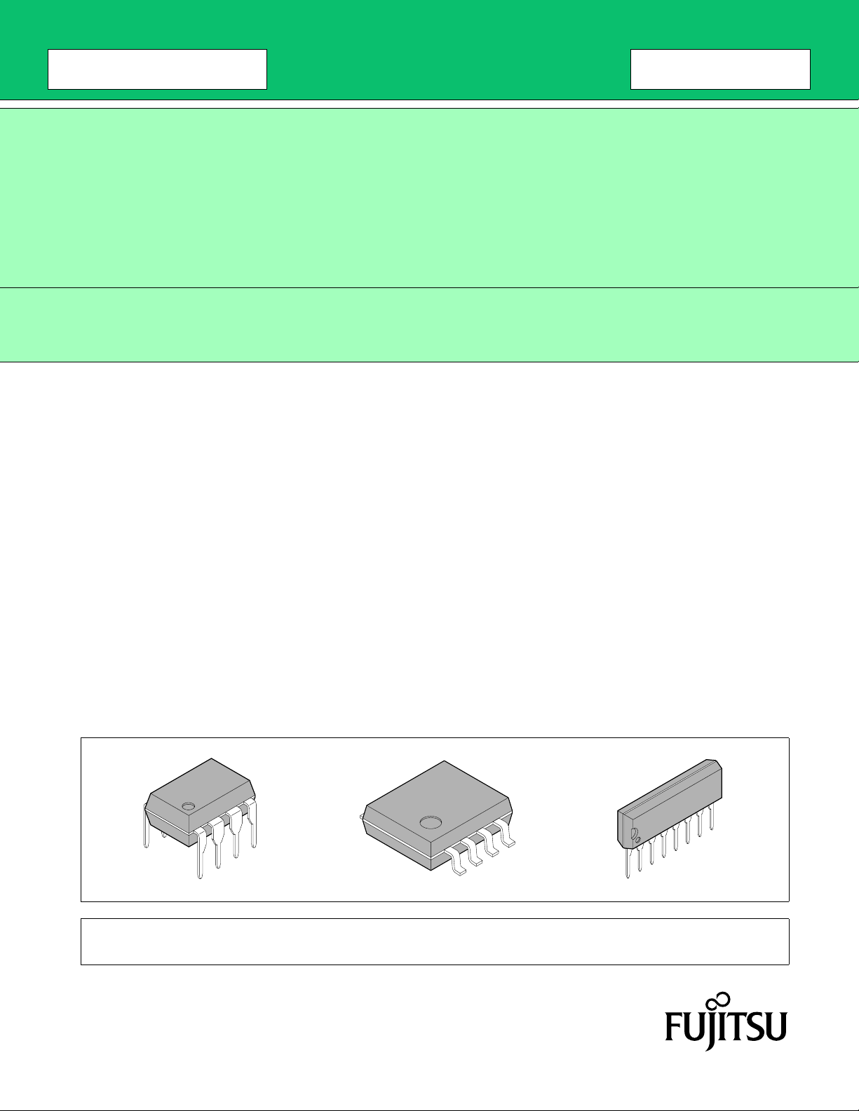
PACKAGES
■
(DIP-8P-M01)
CC = 0.8 V Typ)
(FPT-8P-M01)
(SIP-8P-M03)
This device contains circuitry to protect the inputs against damage due to high static voltages or electric fields.
However, it is advised that normal precautions be taken to avoid application of any voltage higher than maximum rated voltages
to this high impedance circuit.
Page 2
MB3773
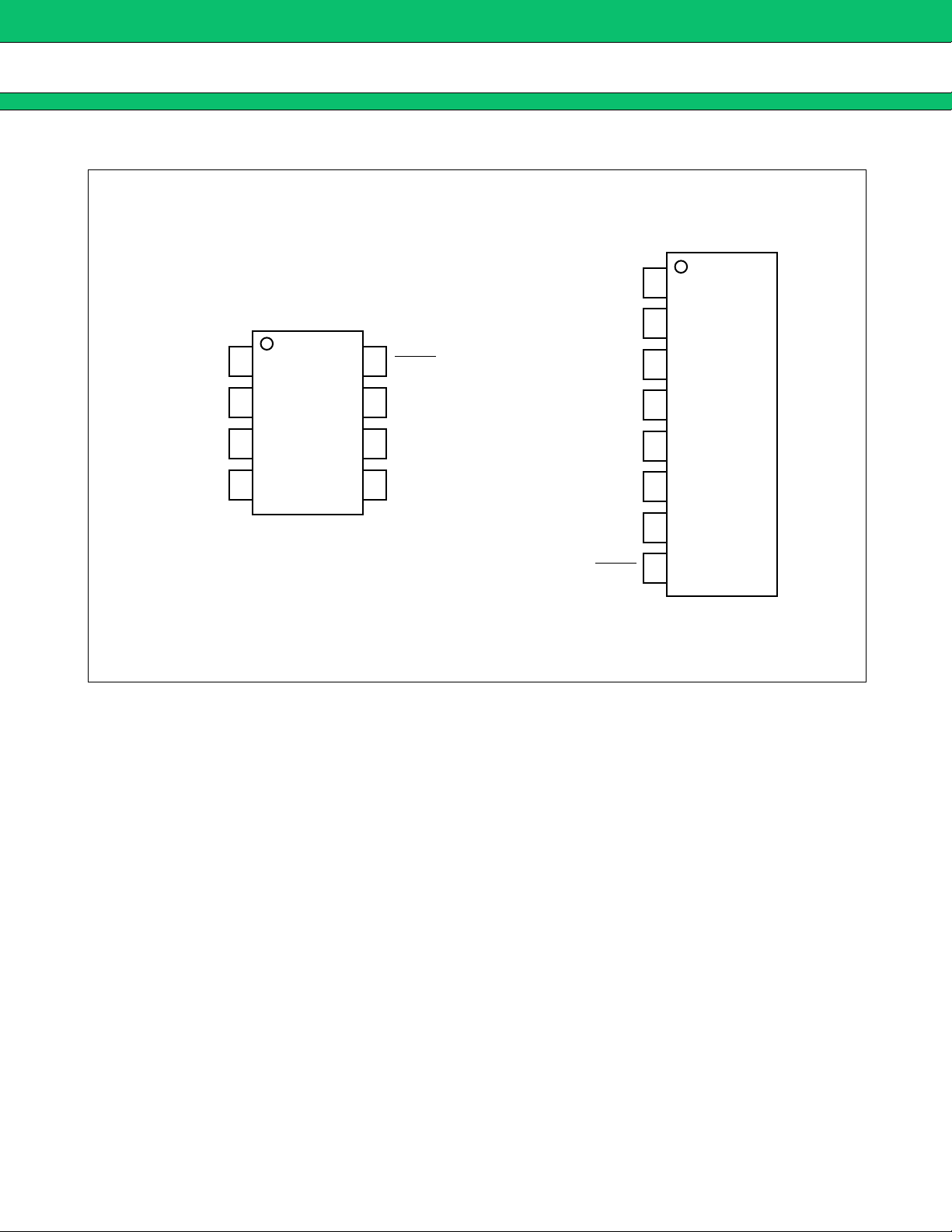
PIN ASSIGNMENT
■■■■
(TOP VIEW)
C
RESET
(FRONT VIEW)
1
T
2
C T
RESET
CK
GND
1
2
3
4
(DIP-8P-M01)
(FPT-8P-M01)
8
RESET
7
V S
6
V REF
5
V CC
CK
GND
V CC
V REF
V S
RESET
3
4
5
6
7
8
(SIP-8P-M03)
2
Page 3
BLOCK DIAGRAM
■■■■
:= 100
kΩ
:= 1.24 V
COMP.S
VCC
5
Reference Voltage Generator
:= 1.2 µA
+
_
:= 1.24 V
COMP.O
+
_
:= 10 µA
MB3773
Reference AMP.
+
_
:=
10 µA
V
REF
6
VS
CK
+
7
_
R
Q
S
:= 40 kΩ
Inhibit
3
Watch
Dog
Timer
P.G
4
GND
2
RESET
CT
1
8
RESET
3
Page 4

MB3773
FUNCTIONAL DESCRIPTIONS
■■■■
Comp.S is comparator including h ysteresis. it compare the ref erence voltage and the v oltage of Vs, so that when
the voltage of Vs terminal falls below approximately 1.23 V, reset signal outputs.
Instantaneous breaks or drops in the power can be detected as abnormal conditions by the MB3773 within a
2 µs interval.
Howev er because momentary breaks or drops of this duration do not cause problems in actual systems in some
cases, a delayed trigger function can be created by connecting capacitors to the Vs terminal.
Comp.O is comparator f or turning on/off the output and, compare the voltage of the Cr terminal and the threshold
voltage. Because the RESET/RESET
pull-up resistor when connected to a high impedance load such as CMOS logic IC.
(It corresponds to 500 kΩ at Vcc = 5 V.) when the voltage of the CK terminal changes from the “high” level into
the “Low” level, pulse generator is sent to the watch-dog timer by generating the pulse momentarily at the time
of drop from the threshold level.
When power-supply voltages fall more than detecting voltages, the watch-dog timer becomes a interdiction.
The Reference amplifier is a op-amp to output the reference voltage.
If the comparator is put up outside, two or more power-supply voltage monitor and overvoltage monitor can be
done.
If it uses a comparator of the open-collector output, and the output of the comparator is connected with the Vs
terminal of MB3773 without the pull-up resistor, it is possible to voltage monitor with reset-hold time.
outputs have b uilt-in pull-up circuit, there is no need to connect to external
4
Page 5
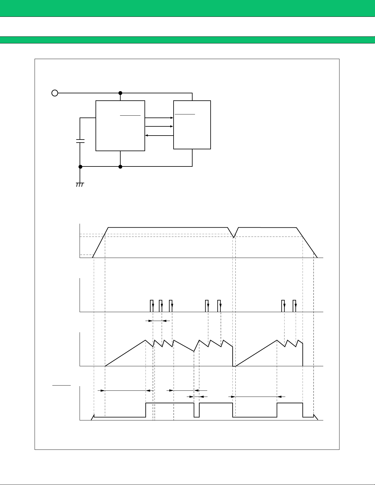
••••
MB3773 Basic Operation
VCC
MB3773
VCC
0.8 V
CK
VSH
VSL
VCC
Logic Circuit
TPR (ms) := 1000 · CT (µF)
C
T
RESET
RESET
CK
GND
RESET
RESET
CK
T
WD (ms) := 100 · CT (µF)
T
WR (ms) := 20 · CT (µF)
Example : C
T = 0.1 µF
T
RR (ms) := 100 (ms)
T
WD (ms) := 10 (ms)
T
WR (ms) := 2 (ms)
C
RESET
TCK
T
TPR
(1) (2) (3)(4)(5) (5) (6)(7) (8)(9) (10) (11) (12)
TWD
TWR TPR
5
Page 6

MB3773
OPERATION SEQUENCE
■■■■
(1) When Vcc rises to about 0.8 V, RESET goes “Low” and RESET goes “High”.
The pull-up current of approximately 1 µA (Vcc = 0.8 V) is output from RESET.
(2) When Vcc rises to VSH ( := 4.3V) , the charge with CT starts.
At this time, the output is being reset.
(3) When C
After T
Reset hold time: T
After releasing reset, the discharge of C
T
T begins charging, RESET goes “High” and RESET goes “Low”.
PR reset of the output is released.
PR (ms) := 1000 × CT (µF)
T starts, and watch-dog timer operation starts.
PR is not influenced by the CK input.
(4) C changes from the discharge into the charge if the clock (Negative edge) is input to the CK terminal
while discharging C
(5) C changes from the charge into the discharge when the voltage of C
T.
T reaches a constant
threshold ( := 1.4 V) .
(4) and (5) are repeated while a normal clock is input by the logic system.
(6) When the clock is cut off, gets, and the voltage of C
T falls on threshold ( := 0.4 V) of reset on, RESET goes
“Low” and RESET goes “High”.
Discharge time of C
T
WD (ms) := 100 × CT (µF)
Because the charging time of C
of reset of the clock, T
(7) Reset time in operating watch-dog timer:T
T until reset is output: TWD is watch-dog timer monitoring time.
T is added at accurate time from stop of the clock and getting to the output
WD becomes maximum TWD + TWR by minimum TWD.
WR is charging time where the voltage of CT goes up to off
threshold ( := 1.4 V) for reset.
T
WR (ms) := 20 × CT (µF)
Reset of the output is released after C
T reaches an off threshold for reset, and CT starts the discharge,
after that if the clock is normally input, operation repeats (4) and (5) , when the clock is cut off, operation
repeats (6) and (7) .
(8) When Vcc falls on V
SL ( := 4.2 V) , reset is output. CT is rapidly discharged of at the same time.
(9) When Vcc goes up to V
SH, the charge with CT is started.
When Vcc is momentarily low,
After falling V
SL or less Vcc, the time to going up is the standard value of the Vcc input pulse width in VSH or
more.
After the charge of C
T is discharged, the charge is started if it is TPI or more.
(10) Reset of the output is released after TPR, after Vcc becomes VSH or more, and the watch-dog timer starts.
After that, when Vcc becomes V
(11) While power supply is off, when Vcc becomes V
SL or less, (8) to (10) is repeated.
SL or less, reset is output.
(12) The reset output is maintained until Vcc becomes 0.8 V when Vcc falls on 0 V.
6
Page 7
ABSOLUTE MAXIMUM RATINGS
■■■■
MB3773
Parameter Symbol
Unit
Min Max
Rating
Supply voltage V
CC − 0.3 + 18 V
V
S − 0.3 VCC + 0.3 ( ≤ +18) V
Input voltage
V
CK − 0.3 + 18 V
RESET, RESET Supply voltage VOH − 0.3 VCC + 0.3 ( ≤ +18) V
Power dissipation (Ta ≤ +85 °C) P
Storage temperature T
D 200 mW
STG − 55 + 125 °C
WARNING: Semiconductor devices can be permanently damaged by application of stress (voltage, current,
temperature, etc.) in excess of absolute maximum ratings. Do not exceed these ratings.
RECOMMENDED OPERATING CONDITIONS
■■■■
Value
Parameter Symbol
Unit
Min Max
Supply voltage V
CC + 3.5 + 16 V
RESET, RESET
REF
V
output current IOUT − 200 + 5 µA
Watch clock setting time t
CK Rising/falling time t
sink current IOL 020mA
WD 0.1 1000 ms
,
FC
tRC 100 µs
Terminal capacitance CT 0.001 10 µF
Operating ambient temperature Ta − 40 + 85 °C
WARNING: The recommended operating conditions are required in order to ensure the normal operation of the
semiconductor device. All of the device’s electrical characteristics are warranted when the device is
operated within these ranges.
Always use semiconductor devices within their recommended operating condition ranges. Operation
outside these ranges may adversely affect reliability and could result in device failure.
No warranty is made with respect to uses, operating conditions, or combinations not represented on
the data sheet. Users considering application outside the listed conditions are advised to contact their
FUJITSU representatives beforehand.
7
Page 8
MB3773
ELECTORICAL CHARACTERISTICS
■■■■
(1) DC Characteristics
Parameter Symbol Condition
(
VCC = 5 V, Ta = + 25 °C)
Value
Min Typ Max
Unit
Supply current I
CC Watch dog timer operating 600 900 µA
V
SL
VCC 4.10 4.20 4.30
Ta = − 40 °C to + 85 °C 4.05 4.20 4.35
Detection voltage
SH
V
VCC 4.20 4.30 4.40
V
Ta = − 40 °C to + 85 °C 4.15 4.30 4.45
Hysteresis width VHYS VCC 50 100 150 mV
1.227 1.245 1.263
Reference voltage V
REF
V
Ta = − 40 °C to + 85 °C 1.215 1.245 1.275
Reference voltage change rate ∆VREF1 VCC = 3.5 V to 16 V 310mV
Reference voltage output
loading change rate
CK threshold voltage V
∆V
REF2 IOUT = − 200 µA to + 5 µA − 5 + 5mV
TH Ta = − 40 °C to + 85 °C 0.8 1.25 2.0 V
IIH VCK = 5.0 V 01.0
CK input current
C
T discharge current ICTD
IL VCK = 0.0 V − 1.0 − 0.1
I
Watch dog timer operating
V
CT = 1.0 V
71014µA
µA
High level output voltage
Output saturation voltage
Output sink current
C
T
charge current ICTU
Min supply voltage for RESET
Min supply voltage for RESET V
8
OH1 VS open, IRESET
V
= − 5 µA4.54.9
VOH2 VS = 0 V, IRESET = − 5 µA4.54.9
V
OL1 VS = 0 V, IRESET = 3 mA 0.2 0.4
OL2 VS = 0 V, IRESET = 10 mA 0.3 0.5
V
VOL3 VS
VOL4 VS
OL1 VS = 0 V, VRESET = 1.0 V 20 60
I
IOL2 VS
VCCL1
CCL2
open, IRESET = 3 mA 0.2 0.4
open, IRESET = 10 mA 0.3 0.5
open, VRESET = 1.0 V 20 60
Power on reset operating
V
CT = 1.0 V
VRESET = 0.4 V,
I
RESET = 0.2 mA
VRESET = VCC − 0.1 V,
R
L (pin 2 − GND) = 1 MΩ
0.5 1.2 2.5 µA
0.8 1.2 V
0.8 1.2 V
V
V
mA
Page 9
(2)AC Characteristics
Parameter Symbol Condition
MB3773
(
VCC = 5 V, Ta = + 25 °C)
Value
Min Typ Max
Unit
V
CC
input pulse width TPI
CK input pulse width T
CK input frequency T
CKW
CK 20 µs
VCC
CK
5 V
4 V
or
8.0 µs
3.0 µs
Watch dog timer watching time TWD CT = 0.1 µF 5 10 15 ms
Watch dog timer reset time T
Rising reset hold time T
Output propagation
delay time from V
CC
Output rising time* t
Output falling time* t
WR CT = 0.1 µF123ms
PR
TPD1
T
PD2
R
F
CT = 0.1 µF, VCC
RESET, RL = 2.2 kΩ,
C
L = 100 pF
RESET, RL = 2.2 kΩ,
C
L = 100 pF
RL = 2.2 kΩ,
C
L = 100 pF
RL = 2.2 kΩ,
C
L = 100 pF
50 100 150 ms
210
310
1.0 1.5
0.1 0.5
* : Output rising/falling time are measured at 10 % to 90 % of voltage.
µs
µs
9
Page 10

MB3773
TYPICAL CHARACTERISTIC CURVES
■■■■
Supply current vs. Supply voltage
0.75
0.65
0.55
0.45
0.35
0.25
0.15
Supply current ICC (mA)
04.02.06.08.010.012.014.016.018.020.0
Ta =+25 °C
Ta =−40 °C
Ta =+25 °C
Ta =+85 °C
Ta =+85 °C
Ta =−40 °C
Supply voltage VCC (V)
Output voltage vs. Supply voltage
(RESET terminal)
Pull up 2.2 kΩ
RESET (V)
6.0
5.0
4.0
CT =0.1 µF
Output voltage vs. Supply voltage
6.0
5.0
4.0
RESET (V)
3.0
2.0
1.0
Ta = −40 °C, +25 °C, +85 °C
(RESET terminal)
Pull up 2.2 kΩ
Output voltage V
01.02.03.04.05.06.07.0
Supply voltage VCC (V)
Detection voltage
SH
(V
, VSL) vs. Temperature
4.50
4.44
4.30
SH, VSL (V)
(RESET, RESET terminal)
VSH
VSL
3.0
2.0
Ta = +85 °C
1.0
Output voltage V
01.02.03.04.05.06.07.0
Ta = +25 °C
Ta = −40 °C
Supply voltage VCC (V)
Output saturation voltage
vs. Output sink current
(RESET terminal)
Ta = −40 °C
400
300
200
100
0 2.0 10.0 12.0 14.0 16.04.0 6.0 8.0 18.0
Output saturation voltage VOL2 (mV)
Output sink current IOL2 (mA)
Ta = +25 °C
Ta = +85 °C
C T = 0.1µF
4.20
4.10
4.00
Detection voltage V
−40−20020406080100
Temperature Ta ( °C)
Output saturation voltage
vs. Output sink current
(RESET terminal)
500
OL2 (mV)
400
300
200
100
Output saturation voltage V
0 2.0 10.0 12.0 14.0 16.04.06.08.018.0
Ta = −40 °C
Ta = +25 °C
Ta = +85 °C
Output sink current IOL8 (mA)
CT = 0.1µF
10
(Continued)
Page 11

MB3773
High level output voltage VOH2 (V)
Reference voltage VREF (V)
High level output voltage
vs. High level output current
5.0
4.5
4.0
0−5−10−15
Ta = −40 °C
High level output current IOH2 (µA)
(RESET
Ta = +25 °C
T = 0.1 µF
C
Ta = +85 °C
Reference voltage
vs. Supply voltage
1.246
1.244
1.242
1.240
1.238
1.236
1.234
03.05.07.09.013.011.017.019.021.015.0
Supply voltage VCC (V) Reference current IREF (µA)
Ta = +25 °C
Ta = +85 °C
Ta = −40 °C
C
T = 0.1 µF
terminal)
High level output voltage
vs. High level output current
5.0
OH8 (V)
4.5
High level output voltage V
4.0
0−5−10−15
Ta = −40 °C
High level output current IOH8 (µA)
(RESET terminal)
Reference voltage
vs. Reference current
1.255
1.250
REF (V)
Ta = +25 °C
1.245
1.240
Reference voltage V
0−40−80−120−160−200−240
Ta = +85 °C
Ta = −40 °C
T = 0.1 µF
C
Ta = +25 °C
Ta = +85 °C
CT = 0.1 µF
Reference voltage
vs. Temperature
1.27
1.26
REF (V)
1.25
1.24
1.23
1.22
Reference voltage V
1.21
−20020−40
Temperature Ta ( °C)
406080100
Rising reset hold time TPR (ms)
Rising reset hold time
vs. Temperature
160
140
120
100
80
60
40
0
−20020−40406080100
Temperature Ta ( °C)
VCC = 5 V
CT = 0.1 µF
(Continued)
11
Page 12

MB3773
(Continued)
3
(ms)
2
WR
Reset time vs.
Temperature
(At watch dog timer)
VCC = 5 V
CT = 0.1 µF
Watchdog timer watching time
vs. Temperature
16
14
12
(ms)
WD
10
8
CC=5 V
V
CT=0.1 µF
1
Reset time T
0
−40−20200406080100
Temperature Ta ( °C)
T
C
terminal capacitance
vs.
Watchdog timer watching time
6
10
5
10
4
10
3
(ms)
10
WD
2
10
1
10
0
10
Watch dog timer
−1
10
watching time T
−2
10
−3
10
CT t
erminal capacitance CT (µF)
10
−3
10
Ta = −40 °C
+25 °C
−2
−1
10
10
0
Ta =
10
+85 °C
1
10
2
CT terminal capacitance
vs. Reset time
(at watch dog timer)
2
10
1
10
(ms)
WR
0
10
Ta =
−1
−40 °C
10
Reset time T
−2
10
−3
10
CT t
−
3
−
2
−
10
1
10
10
10
erminal capacitance CT (µF)
6
Watch dog timer
watching time T
4
0
−40−20200406080100
(ms)
PR
Ta = +25 °C
+85 °C
Rising reset hold time T
0
1
2
10
10
Temperature Ta ( °C)
CT terminal capacitance
vs. Rising reset hold time
6
10
5
10
4
10
3
10
2
10
Ta = −40 °C
1
10
0
10
−1
10
−2
10
−3
10
CT t
erminal capacitance CT (µF)
10
−3
10
Ta = +25 °C
−2
−1
10
10
0
+85 °C
1
10
10
2
12
Page 13

APPLICATION CIRCUIT
■■■■
EXAMPLE 1: Monitoring 5V Supply Voltage and Watchdog Timer
VCC (5V)
MB3773
MB3773
1
2
3
C
T
4
8
7
6
5
Notes : • Supply voltage is monitored using VS.
• Detection voltage are V
SH and VSL.
EXAMPLE 2: 5V Supply Voltage Monitoring (external fine-tuning type)
VCC (5V)
MB3773
R1
Logic circuit
RESET
RESET
CK
GND
Logic circuit
CT
1
2
3
4
8
7
6
5
R2
Notes : • Vs detection voltage can be adjusted externally.
• Based on selecting R
1 and R2 values that are sufficiently lower than the resistance of the IC’s
internal voltage divider, the detection voltage can be set according to the resistance ratio of
R
1 and R2 (See the table below.)
ΩΩΩΩ
R1 (k
)R
2
ΩΩΩΩ
(k
) Detection voltage: VSL (V) Detection voltage: VSH (V)
10 3.9 4.4 4.5
9.1 3.9 4.1 4.2
RESET
RESET
CK
GND
13
Page 14

MB3773
(a)
V
EXAMPLE 3: With Forced Reset (with reset hold)
CC
MB3773
1
2
3
C
T
Note : Grounding pin 7 at the time of SW ON sets RESET (pin 8) to Low and RESET (pin 2) to High.
(b)
VCC
Cr
4
MB3773
1
2
3
4
8
7
6
5
8
7
6
5
Tr
SW
10 kΩ
10 kΩ
RESET
RESET
CK
Logic circuit
GND
RESET
RESET
CK
GND
Logic circuit
14
RESIN
Note : Feeding the signal to terminal RESIN and turning on Tr sets the RESET terminal to Low and
the RESET terminal to High.
Page 15

VCC2(12 V)
V
CC1 (5 V)
MB3773
EXAMPLE 4: Monitoring Two Supply Voltages (with hysteresis, reset output and NMI)
MB3773
1
2
C
T
3
4
Example : Comp. 1, Comp. 2
: MB4204, MB47393
8
7
6
5
1.2 kΩ
1
R
5.1 kΩ
R2
4.7 kΩ
R
5
30 kΩ
R
3
180 kΩ
R
4
+
_
Comp. 1
10 kΩ
R6
+
_
Comp. 2
RESET
RESET
CK
or port
NMI
GND
Logic circuit
Notes : • The 5 V supply voltage is monitored by the MB3773.
• The 12 V supply voltage is monitored by the external circuit. Its output is connected to the NMI
terminal and, when voltage drops, Comp. 2 interrupts the logic circuit.
• Use V
CC1 ( = 5 V) to power the comparators (Comp. 1 and Comp. 2) in the external circuit shown
above.
• The detection voltage of the V
CC2 ( = 12 V) supply voltage is approximately 9.2 V/9.4 V and has
a hysteresis width of approximately 0.2 V.
V
CC2 detection voltage and hysteresis width can be found using the following formulas:
→ Detection voltage
→ Hysteresis width V
R3 + (R4 // R5)
V2H =
V2L =
HYS = V2H − V2L
R
4 // R5
R3 + R5
R5
× VREF
× VREF
(Approximately 9.4 V in the above illustration)
(Approximately 9.2 V in the above illustration)
15
Page 16

MB3773
EXAMPLE 5: Monitoring Two Supply Voltages (with hysteresis and reset output)
VCC2 (12 V)
VCC1 (5 V)
1
2
CT
3
4
Example : Comp. 1, Comp. 2
: MB4204, MB47393
MB3773
1.2 kΩ
R
5.1 kΩ
R
20 kΩ
R
6
8
7
6
5
30 kΩ
R3
Diode
RESET
RESET
CK
Logic circuit
GND
180 kΩ
R
4
+
_
+
_
Comp. 1
1
Comp. 2
4.7 kΩ
2
R
5
16
Notes : • When either 5 V or 12 V supply voltage decreases below its detection voltage (V
the MB3773 RESET terminal is set to High and the MB3773 RESET
• Use V
CC1 ( = 5 V) to power the comparators (Comp. 1 and Comp. 2) in the external circuit shown
terminal is set to Low.
above.
• The detection voltage of the V
CC2 ( = 12 V) supply voltage is approximately 9.2 V/9.4 V and has a
hysteresis width of approximately 0.2 V. For the formulas for finding hysteresis width and detection
voltage, see section 4.
SL),
Page 17

VCC (5 V)
MB3773
EXAMPLE 6: Monitoring Low voltage and Overvoltage Monitoring (with hysteresis)
CT
MB3773
1
2
3
4
8
7
6
5
1.2 kΩ
R
1
5.6 kΩ
R
6
4.7 kΩ
R
5
30 kΩ
R
3
180 kΩ
R
4
+
_
Comp. 1
Diode
Comp. 2
RESET
20 kΩ
R
6
Logic circuit
RESET
RESET
CK
GND
_
+
Example : Comp. 1, Comp. 2
: MB4204, MB47393
0
1L V1H
V
V2L V2H
VCC
Notes : • Comp. 1 and Comp. 2 are used to monitor for overvoltage while the MB3773 is used to monitor
for low voltage. Detection voltages V
Detection voltages V
2L/V2H at the time of overvoltage are approximately 6.0 V/6.1 V.
1L/V1H at the time of low voltage are approximately 4.2 V/4.3 V.
For the formulas for finding hysteresis width and detection voltage, see EXAMPLE 4.
• Use V
CC ( = 5 V) to power the comparators (Comp. 1 and Comp. 2) in the external circuit shown
above.
17
Page 18

MB3773
EXAMPLE 7: Monitoring Supply Voltage Using Delayed Trigger
VCC
5V
4V
Note : Adding voltage such as shown in the figure to VCC increases the minimum input pulse
V
CC
CT
width by 50 µs (C
MB3773
1
2
3
4
1 = 1000 pF).
8
7
6
5
C1
RESET
RESET
CK
GND
Logic circuit
18
Page 19

MB3773
EXAMPLE 8: Stopping Watch-dog Timer (Monitoring only supply voltage)
These are example application circuits in which the MB3773 monitors supply voltage alone without resetting the
microprocessor even if the latter, used in standby mode, stops sending the clock pulse to the MB3773.
• The watch-dog timer is inhibited by clamping the C
The supply voltage is constantly monitored even while the watch-dog timer is inhibited.
For this reason, a reset signal is output at the occurrence of either instantaneous disruption or a sudden drop
to low voltage.
Note that in application examples (a) and (b), the hold signal is inactive when the watch-dog timer is inhibited at
the time of resetting.
If the hold signal is active when tie microprocessor is reset, the solution is to add a gate, as in examples (c)
and (d).
(a) Using NPN transistor
VCC(5 V)
T terminal voltage to VREF.
CT
(b) Using PNP transistor
VCC (5 V)
MB3773
1
2
3
4
MB3773
1
2
3
4
8
7
6
5
R2=1 kΩ
8
7
6
5
Logic circuit
RESET
RESET
CK
HALT
GND
R1=1 MΩ
Logic circuit
RESET
RESET
CK
HALT
CT
R2=1 kΩ
GND
R1=51 kΩ
(Continued)
19
Page 20

MB3773
(Continued)
(c) Using NPN transistor
VCC (5 V)
CT
(d) Using PNP transistor
VCC (5 V)
MB3773
1
2
3
4
8
7
6
5
R2=1 kΩ
R
1=1 MΩ
Logic circuit
RESET
RESET
CK
HALT
GND
20
CT
MB3773
1
2
3
4
8
7
6
5
R2=1 kΩ
R1=51 kΩ
Logic circuit
RESET
RESET
CK
HALT
GND
Page 21

VCC( = 5 V)
MB3773
EXAMPLE 9: Reducing Reset Hold Time
VCC ( = 5 V)
CT
MB3773
1
2
3
4
8
7
6
RESET
RESET
CK
5
Logic circuit
GND
(a) TPR reduction method
Notes : • RESET is the only output that can be used.
• Standard T
Formulas:T
PR, TWD and TWR value can be found using the following formulas.
PR (ms) := 100 × CT (µF)
T
WD (ms) := 100 × CT (µF)
T
WR (ms) := 16 × CT (µF)
• The above formulas become standard values in determining T
Reset hold time is compared below between the reduction circuit and the standard circuit.
CT
MB3773
1
2
3
4
8
7
6
5
(b) Standard usage
PR, TWD and TWR.
Logic circuit
RESET
RESET
CK
GND
CT = 0.1 µF
PR
reduction circuit Standard circuit
T
T
PR := 10 ms 100 ms
T
WD := 10 ms 10 ms
T
WR := 1.6 ms 2.0 ms
21
Page 22

MB3773
EXAMPLE 10: Circuit for Monitoring Multiple Microprocessor
FF3FF2FF1
D
1
CK1
S
Q
1
Q1
R
2
D
CK2
S
Q
2
Q2
R
***
RESET
RESET
CK
GND
RESET
RESET
CK
GND
RESET
RESET
CK
GND
*: Microprocessor
D
3
CK3
VCC ( = 5 V)
S
Q
3
Q3
R
R2
R1
1
8
2
7
3
CT
6
4
5
MB3773
Figure 1
22
Notes : • connects from FF1 and FF2 outputs Q1 and Q2 to the NOR input.
• Depending on timing, these connections may not be necessary.
• Example : R
1 = R2 = 2.2 kΩ
C
T = 0.1 µF
CK1
Q1
CK2
Q2
CK3
Q3
NOR
Output
Figure 2
Page 23

MB3773
Description of Application Circuits
Using one MB3773, this application circuit monitors multiple microprocessor in one system. Signals from each
microprocessor are sent to FF1, FF2 and FF3 clock inputs. Figure 2 shows these timings . Each flip-flop operates
using signals sent from microprocessor as its clock pulse. When even one signal stops, the relevant receiving
.
3
flip-flop stops operating. As a result, cyclical pulses are not generated at output Q
arriving at the CK terminal of the MB3773, the MB3773 generates a reset signal.
Note that output Q
are f
1, f2 and f3 respectively.
1
---f
3 frequency f will be in the following range , where the clock frequencies of CK1, CK2 and CK3
1
1
1
-- -
----
f
0
f
1
1
++≤≤
----
----
f
f
2
3
Since the clock pulse stops
where f
0
is the lowest frequency among f1, f2 and f3.
23
Page 24

MB3773
EXAMPLE 11: Circuit for Limiting Upper Clock Input Frequency
VCC (5 V)
R2
CT
1
2
3
4
8
7
6
5
R1=10 kΩ
Tr1
C2
Notes : • This is an example application to limit upper frequency f
the microprocessor.
If the CK cycle sent from the microprocessor exceeds f
(The lower frequency has already been set using C
T.)
• When a clock pulse such as shown below is sent to terminal CK, a short T
from reaching the CK input threshold level ( := 1.25 V), and will cause a reset signal to be output.
The T
1 value can be found using the following formula :
T1 := 0.3 C2R2
where VCC = 5 V, T3 ≥ 3.0 µs, T2 ≥ 20 µs
T2
RESET
RESET
CK
GND
H of clock pulses sent from
H, the circuit generates a reset signal.
2 prevents C2 voltage
24
CK waveform
C2 voltage
T3
T1
Example : Setting C and R allow the upper
CRT
0.01 µF10 kΩ 30 µs
0.1 µF10 kΩ 300 µs
1
T
value to be set (See the table below).
1
Page 25

MB3773
NOTES ON USE
■■■■
• Take account of common impedance when designing the earth line on a printed wiring board.
• Take measures against static electricity.
- For semiconductors, use antistatic or conductive containers.
- When storing or carrying a printed circuit board after chip mounting, put it in a conductive bag or container.
- The work table, tools and measuring instruments must be grounded.
- The worker must put on a grounding device containing 250 kΩ to 1 MΩ resistors in series.
• Do not apply a negative voltage
- Applying a negative voltage of −0.3 V or less to an LSI may generate a parasitic transistor, resulting in
malfunction.
ORDERING INFORMATION
■■■■
Part number Package Remarks
MB3773P
8-pin plastic DIP
(DIP-8P-M01)
MB3773PS
MB3773PF
8-pin plastic SIP
(SIP-8P-M03)
8-pin plastic SOP
(FPT-8P-M01)
25
Page 26

MB3773
PACKAGE DIMENSIONS
■■■■
8-pin plastic DIP
(DIP-8P-M01)
9.40
.370
+0.40
–0.30
+.016
–.012
1 PIN INDEX
4.36(.172)MAX
3.00(.118)MIN
+0.30
0.99 1.52
–0
+.012
–0
.039
+0.35
0.89
–0.30
+.014
–.012
.035
C
1994 FUJITSU LIMITED D08006S-2C-3
2.54(.100)
.060 –0
TYP
6.20±0.25
(.244±.010)
0.51(.020)MIN
0.46±0.08
(.018±.003)
+0.30
–0
+.012
0.25±0.05
(.010±.002)
7.62(.300)
TYP
15°MAX
Dimensions in mm (inches) .
Note : The values in parentheses are reference values.
(Continued)
26
Page 27

8-pin plastic FPT
(FPT-8P-M01)
MB3773
Note 1 : *1 : These dimensions include resin protrusion.
Note 2 : *2 : These dimensions do not include resin protrusion.
Note 3 : Pins width and pins thickness include plating thickness.
Note 4 : Pins width do not include tie bar cutting remainder.
+.010
+0.25
1
6.35
*
–0.20
.250
INDEX
–.008
58
2
*
(.209±.012) (.307±.016)
7.80±0.405.30±0.30
0.17
.007
+0.03
–0.04
+.001
–.002
Details of "A" part
2.00
.079
+0.25
–0.15
(Mounting height)
+.010
–.006
14
1.27(.050)
C
2002 FUJITSU LIMITED F08002S-c-6-7
0.10(.004)
0.10(.004)
0.47±0.08
(.019±.003)
0.13(.005)
"A"
M
0.25(.010)
0~8˚
0.50±0.20
(.020±.008)
0.60±0.15
(.024±.006)
+0.10
–0.05
0.10
+.004
–.002
.004
(Stand off)
Dimensions in mm (inches) .
Note : The values in parentheses are reference values.
(Continued)
27
Page 28

MB3773
(Continued)
8-pin plastic SIP
(SIP-8P-M03)
19.65
.774
INDEX-1
INDEX-2
+0.30
0.99
–0
+.012
–0
.039
+0.30
2.54(.100)
TYP
C
1994 FUJITSU LIMITED S08010S-3C-2
1.52
.060
–0
+.012
–0
+0.15
–0.35
+.006
–.014
3.26±0.25
(.128±.010)
6.20±0.25
(.244±.010)
8.20±0.30
(.323±.012)
4.00±0.30
(.157±.012)
0.50±0.08
(.020±.003)
0.25±0.05
(.010±.002)
Dimensions in mm (inches) .
Note : The values in parentheses are reference values.
28
Page 29

MB3773
FUJITSU LIMITED
All Rights Reserved.
The contents of this document are subject to change without notice.
Customers are advised to consult with FUJITSU sales
representatives before ordering.
The information, such as descriptions of function and application
circuit examples, in this document are presented solely for the
purpose of reference to show examples of operations and uses of
Fujitsu semiconductor device; Fujitsu does not warrant proper
operation of the device with respect to use based on such
information. When you develop equipment incorporating the
device based on such information, you must assume any
responsibility arising out of such use of the information. Fujitsu
assumes no liability for any damages whatsoever arising out of
the use of the information.
Any information in this document, including descriptions of
function and schematic diagrams, shall not be construed as license
of the use or exercise of any intellectual property right, such as
patent right or copyright, or any other right of Fujitsu or any third
party or does Fujitsu warrant non-infringement of any third-party’s
intellectual property right or other right by using such information.
Fujitsu assumes no liability for any infringement of the intellectual
property rights or other rights of third parties which would result
from the use of information contained herein.
The products described in this document are designed, developed
and manufactured as contemplated for general use, including
without limitation, ordinary industrial use, general office use,
personal use, and household use, but are not designed, developed
and manufactured as contemplated (1) for use accompanying fatal
risks or dangers that, unless extremely high safety is secured, could
have a serious effect to the public, and could lead directly to death,
personal injury, severe physical damage or other loss (i.e., nuclear
reaction control in nuclear facility, aircraft flight control, air traffic
control, mass transport control, medical life support system, missile
launch control in weapon system), or (2) for use requiring
extremely high reliability (i.e., submersible repeater and artificial
satellite).
Please note that Fujitsu will not be liable against you and/or any
third party for any claims or damages arising in connection with
above-mentioned uses of the products.
Any semiconductor devices have an inherent chance of failure. You
must protect against injury, damage or loss from such failures by
incorporating safety design measures into your facility and
equipment such as redundancy, fire protection, and prevention of
over-current levels and other abnormal operating conditions.
If any products described in this document represent goods or
technologies subject to certain restrictions on export under the
Foreign Exchange and Foreign Trade Law of Japan, the prior
authorization by Japanese government will be required for export
of those products from Japan.
F0308
FUJITSU LIMITED Printed in Japan
 Loading...