

Page 1

The following document contains information on Cypress products.
Page 2
FUJITSU SEMICONDUCTOR
SUPPORT SYSTEM
SS01-44007-1E
®
LQFP-120P DAUGHTER BOARD
MB2031-20
OPERATION MANUAL
Page 3

Page 4
PREFACE
Thank you for purchasing the MB2031-20 (F2MC*1-16LX series LQFP-120P*2 USB daughter board
(hereinafter called the daughter board)).
This product is an optional MB2031-01 tool connected to the MB2031-01 (USB evaluation board).
This product is compatible with the following MCUs: F
This manual explains how to use the MB2031-20. Before using the MB2031-20, be sure to read
this manual.
*1: F2MC is the abbreviation of FUJITSU Flexible Microcontroller.
*2: The applicable package is the FPT-120P-M05.
■ Caution of the products described in this document
Cautions in the following correspond to the products described in this document.
2
MC-16LX MB903303 Series (LQFP-120P).
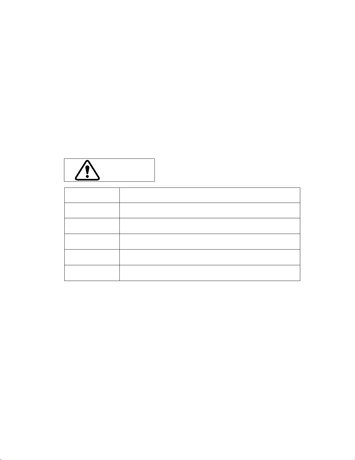
CAUTION
The wrong use of a device will give an injury and may cause
malfunction on customers system.
Cuts
Damage
Damage
Damage
Damage
Damage
This product has parts with sharp points that are exposed.
Do not touch edge of the product with your bare hands.
The method and environment for using this daughter board must conform to the
MB2031-01 specifications, otherwise the daughter board and user system are damaged.
Before setting a mode, be sure to power off all related systems, otherwise the
MCU and user system are damaged.
Before setting the analog pins, be sure to power off all related systems,
otherwise the MCU and user system are damaged.
Before mounting the MCU, be sure to power off all related systems, otherwise
the MCU and user system are damaged.
Before connecting the USB evaluation board, be sure to power off all related
otherwise the USB evaluation board and user system are damaged.
systems,
Page 5

• The contents of this document are subject to change without notice.
Customers are advised to consult with FUJITSU sales representatives before ordering.
• The information, such as descriptions of function and application circuit examples, in this document are presented solely for
the purpose of reference to show examples of operations and uses of Fujitsu semiconductor device; Fujitsu does not warrant
proper operation of the device with respect to use based on such information. When you develop equipment incorporating the
device based on such information, you must assume any responsibility arising out of such use of the information. Fujitsu
assumes no liability for any damages whatsoever arising out of the use of the information.
• Any information in this document, including descriptions of function and schematic diagrams, shall not be construed as license
of the use or exercise of any intellectual property right, such as patent right or copyright, or any other right of Fujitsu or any
third party or does Fujitsu warrant non-infringement of any third-party' s intellectual property right or other right by using such
information. Fujitsu assumes no liability for any infringement of the intellectual property rights or other rights of third parties
which would result from the use of information contained herein.
• The products described in this document are designed, developed and manufactured as contemplated for general use, including
without limitation, ordinary industrial use, general office use, personal use, and household use, but are not designed, developed
and manufactured as contemplated (1) for use accompanying fatal risks or dangers that, unless extremely high safety is secured,
could have a serious effect to the public, and could lead directly to death, personal injury, severe physical damage or other loss
(i.e., nuclear reaction control in nuclear facility, aircraft flight control, air traffic control, mass transport control, medical life
support system, missile launch control in weapon system), or (2) for use requiring extremely high reliability (i.e., submersible
repeater and artificial satellite).
Please note that Fujitsu will not be liable against you and/or any third party for any claims or damages arising in connection
with above-mentioned uses of the products.
• Any semiconductor devices have an inherent chance of failure. You must protect against injury, damage or loss from such
failures by incorporating safety design measures into your facility and equipment such as redundancy, fire protection, and
prevention of over-current levels and other abnormal operating conditions.
• If any products described in this document represent goods or technologies subject to certain restrictions on export under the
Foreign Exchange and Foreign Trade Law of Japan, the prior authorization by Japanese government will be required for export
of those products from Japan.
©2003 FUJITSU LIMITED Printed in Japan
Page 6

1. Checking the Delivered Product
Before using the daughter board, confirm that all of the parts and user's guides listed below are
included in the shipment.
•••• LQFP-120P USB daughter board: 1
•••• HQPACK120SE* (IC Socket cover): 1
•••• HQPACK fixing screws (M2 x 6mm, Supplied with HQPACK120SE): 4
•••• User’s guide (Japanese), (English, this manual): 1
*: This is IC Socket cover of mounting the mass-produced MCU (hereinafter called
HQPACK).
2. Handling Precautions
The daughter board is precision-manufactured to improve dimensional accuracy and to ensure
reliable contact. The daughter board is therefore sensitive to mechanical shock, and must be handled
carefully. To ensure correct use in the appropriate environment, use the products only as instructed in
Section 3, "Using This Daughter Board".
1
Page 7

3. Using This Daughter Board
■ Setting an MCU mode
•••• The mode setting short plug (S2) on the daughter board is used to set the operation mode
(MD0 - MD2 pin) of the MCU mounted on the daughter board.
•••• To set the pin to High, move the short plug to the VCC side.
•••• To set the pin to Low, move the short plug to the GND side.
•••• For details on how to set the operation mode of the mounted MCU, refer to the MCU
hardware manual.
MODE SELECT
GND
S2
VCC
Figure 1 Mode settings
■ Setting the analog power supply pins
The short plug (S1) for analog power supply pin setting on the daughter board is used for switching
analog power supply pins (AVCC/AVRH/AVSS).
For the information on the analog power supply pins of the MCU, refer to the MCU hardware
manual.
ANALOG VCC
AVSS AVRH AVCC
MD0 MD1 MD2
S1
GND VCC VCC
Figure 2 Analog power supply setting
2
Page 8

4. Mountings Mass-production MCU
■ Mounting
To mount the mass production MCU to user's system without an emulator, use an accessory socket
cover (HQPACK120SE).
1. To mount the mass production MCU on the user system, match the first pin (▲) (see
Figure 3) on the NQPACK120SE (hereinafter called NQPACK) mounted on the user
system with the first pin on the mass-produced MCU.
2. Confirm that the MCU is securely mounted on the NQPACK, insert HQPACK with
aligning the direction of the NQPACK and that of the HQPACK as shown in Figure 4.
3. Insert a screw for fixing HQPACK in each of four screw holes and tighten the screws
diagonally.
Tightening the screws too tight might result in a defective contact.
The index mark
on the NQPACK
Figure 3 The index mark no the NQPACK
User system board
Figure 4 Mounting the mass-produced MCU
NOTE : Do not connect a probe header when mounting the MCU.
HQPACK
Screw for securing
HQPACK
Mass-produced MCU
NQPACK
3
Page 9

5. Connecting the USB evaluation board
■ Connection
To connect the USB evaluation board to the daughter board, attach the daughter I/F connector on the
USB evaluation board to the main I/F connector on the daughter board.
The daughter I/F connector has silk-screened symbols A, B1, and B2. The main I/F connector has
silk-screened symbols A and B.
Connect silk-screened symbols A and B1 of the daughter I/F connector correctly to silk-screened
symbols A and B of the main I/F connector.
USB evaluation board Daughter board
A
A
AB
B1
B
B2
Figure 5 USB evaluation board connection
4
Page 10

6. Connector Pin Assignment
Table 1 lists the correspondence between the function pins of the MCU and USB evaluation board.
Table 2 lists the correspondence between the general I/F connector pins of the MCU and USB
evaluation board.
Table 1 Connector pin assignment
MCU USB evaluation board
Pin No. MB9033X Pin name
86 P55/HAKX USB-HUB(D4-) FIFO(Q7)
85 P54/HRQ USB-HUB(D4+) FIFO(Q6)
84 P53/WRHX USB-HUB(D3-) FIFO(Q5)
83 P52/WRLX USB-HUB(D3+) FIFO(Q4)
82 P51/RDX USB-HUB(D2-) FIFO(Q3)
81 P50/ALE USB-HUB(D2+) FIFO(Q2)
77 HVM USB-HUB(D1-) FIFO(Q1)
78 HVP USB-HUB(D1+) FIFO(Q0)
21 P60/INT0 USB-LED(HUB-SUSP) FIFO(xFL/xRT)
20 P47/A15/SCK1 USB-LED(SUSP) FIFO(xFF)
19 P46/A14/SOT1 USB-LED(LINK) FIFO(xEF)
7 P36/A06 RS-232C(DR/RX EN) FIFO(xR)
6 P35/A05 RS-232C(DSR) FIFO(xW)
1 P30/A00/TIN1 RS-232C(RTS) FIFO(D7)
11 P42/A10/SIN0 RS-232C(RD) FIFO(D6)
12 P43/A11/SOT0 RS-232C(TD) FIFO(D5)
17 P44/A12/SCK0 NC FIFO(D4)
94 P01/AD01/D01 USB-HUB(Power4 EN) FIFO(D3)
93 P00/AD00/D00 USB-HUB(Power3 EN) FIFO(D2)
92 P57/CLK USB-HUB(Power2 EN) FIFO(D1)
91 P56/RDY USB-HUB(Power1 EN) FIFO(D0)
5 P34/A04 RS-232C(RI) NC
4 P33/A03/TOT2 RS-232C(CTS) NC
3 P32/A02/TIN2 RS-232C(DCD) NC
18 P45/A13/SIN1 USB-HUB (Power monitor 4 0C) NC
10 P41/A09/TOT0 USB-HUB (Power monitor 3 0C) NC
9 P40/A08/TIN0 USB-HUB (Power monitor 2 0C) NC
8 P37/A07 USB-HUB (Power monitor 1 0C) NC
2 P31/A01/TOT1 RS-232C(DTR) NC
Note : “NC” indicates that the pin is not connected.
Short plug side A Short plug side B
Connection destination function
(Pin name)
Connection destination function
(Pin name)
5
Page 11

Table 2 Pin assignments of general-purpose I/F connectors (continues on next page)
General-purpose I/F
connector A
Pin No.
A1 17 P44/A12/SCK0 B1 12 P43/A11/SOT0
A2 11 P42/A10/SIN0 B2 1 P30/A00/TIN1
A3 2 P31/A01/TOT1 B3 8 P37/A07
A4 9 P40/A08/TIN0 B4 10 P41/A09/TOT0
A5 18 P45/A13/SIN1 B5 3 P32/A02/TIN2
A6 4 P33/A03/TOT2 B6 5 P34/A04
A7 6 P35/A05 B7 - A8 7 P36/A06 B8 19 P46/A14/SOT1
A9 20 P47/A15/SCK1 B9 21 P60/INT0
A10 90 RSTX B10 22 P61/INT1
A11 23 P62/INT2/SIN B11 108 X0
A12 107 X1 B12 - A13 24 P63/INT3/SOT B13 25 P64/INT4/SCK
A14 26 P65/INT5/PWC B14 27 P66/INT6/SCL0
A15 28 P67/INT7/SDA0 B15 29 P90/SIN2
A16 30 P91/SOT2 B16 31 P92/SCK2
A17 32 P93/SIN3 B17 33 P94/SOT3
A18 34 P95/SCK3 B18 35 P96/ADTG/FRCK
A19 36 AVcc B19 37 AVRH
A20 38 AVss B20 39 P70/AN0
A21 40 P71/AN1 B21 41 P72/AN2
A22 42 P73/AN3 B22 43 P74/AN4
A23 44 P75/AN5 B23 45 P76/AN6
A24 46 P77/AN7 B24 48 P80/AN8
A25 49 P81/AN9 B25 50 P82/AN10
A26 51 P83/AN11 B26 52 P84/AN12
A27 53 P85/AN13 B27 54 P86/AN14
A28 - - B28 - A29 - - B29 - A30 - - B30 - -
Pin
No.
MCU MCU
Pin name
General-purpose I/F
connector A
Pin No.
Pin
No.
Pin name
6
Page 12

Table 2 Pin assignments of general-purpose I/F connectors (continued)
General-purpose I/F
connector B
Pin No.
A1 - - B1 - -
A2 - - B2 - -
A3 - - B3 - -
A4 120 P27/A23/PPG3 B4 119 P26/A22/PPG2
A5 118 P25/A21/PPG1 B5 117 P24/A20/PPG0
A6 116 P23/A19 B6 115 P22/A18
A7 114 P21/A17 B7 113 P20/A16
A8 112 P17/AD15/D15 B8 111 P16/AD14/D14
A9 110 P15/AD13/D13 B9 109 P14/AD12/D12
A10 104 P13/AD11/D11 B10 103 P12/AD10/D10
A11 102 P11/AD09/D09 B11 101 P10/AD08/D08
A12 100 P07/AD07/D07 B12 99 P06/AD06/D06
A13 98 P05/AD05/D05 B13 97 P04/AD04/D04
A14 96 P03/AD03/D03 B14 95 P02/AD02/D02
A15 94 P01/AD01/D01 B15 93 P00/AD00/D00
A16 92 P57/CLK B16 91 P56/RDY
A17 86 P55/HAKX B17 85 P54/HRQ
A18 84 P53/WRHX B18 83 P52/WRLX
A19 82 P51/RDX B19 81 P50/ALE
A20 77 HVM B20 78 HVP
A21 73 DVM B21 74 DVP
A22 80 HCONX B22 - A23 70 PB6/PPG5 B23 69 PB5/PPG4
A24 68 PB4 B24 67 PB3/SDA2
A25 66 PB2/SCL2 B25 65 PB1/SDA1
A26 64 PB0/SCL1 B26 63 PA7/OUT3
A27 62 PA6/OUT2 B27 61 PA5/OUT1
A28 60 PA4/OUT0 B28 59 PA3/IN3
A29 58 PA2/IN2 B29 57 PA1/IN1
A30 56 PA0/IN0 B30 55 P87/AN15
Pin
No.
MCU MCU
Pin name
General-purpose I/F
connector B
Pin No.
Pin
No.
Pin name
7
Page 13

8
Page 14

-
-
FUJITSU SEMICONDUCTOR • SUPPORT SYSTEM
F2MC-16LX
LQFP-120P USB DAUGHTER BOARD
MB2031-20
OPERATION MANUAL
April 2003 the first edition
Published
FUJITSU LIMITED
Electronic Devices
Edited Business Promotion Dept.
Page 15

 Loading...