

Page 1

FUJITSU SEMICONDUCTOR
DATA SHEET
ASSP
DS04-21374-1E
Dual S
PLL Frequency
erial Input
Synthesizer
MB15F74UL
DESCRIPTION
■
The Fujitsu MB15F74UL is a serial input Phase Locked Loop (PLL) frequency synthesizer with a 4000 MHz and
a 2000 MHz prescalers. A 64/65 or a 128/129 for the 4000 MHz prescaler, and a 32/33 or a 64/65 for the
2000 MHz prescaler can be selected for the prescaler that enables pulse swallow operation.
The BiCMOS process is used, as a result a supply current is typically 9.0 mA at 3.0 V. The supply voltage range
is from 2.7 V to 3.6 V. A refined charge pump supplies well-balanced output current with 1.5 mA and 6 mA
selectable by serial date. The pin assignments are the same as MB15F78UL. F ast locking is achie ved f or adopting
the new circuit.
The new package (BCC20) decreases a mount area of MB15F74UL more than 30% comparing with the former
BCC16 (for dual PLL) .
FEATURES
■
• High frequency operation : RF synthesizer : 4000 MHz Max
: IF synthesizer : 2000 MHz Max
• Low power supply voltage : VCC = 2.7 to 3.6 V
• Ultra low power supply current : I
PACKAGE
■
CC = 9.0 mA Typ
(VCC = Vp = 3.0 V, Ta = +25 °C, SWIF = SWRF = 0 in IF/RF locking state)
(Continued)
20-pad plastic BCC
(LCC-20P-M05)
Page 2

MB15F74UL
(Continued)
• Direct power saving function : Power supply current in power saving mode
Typ 0.1 µA (V
Max 10 µA (VCC = Vp = 3.0 V)
• Software selectable charge pump current : 1.5 mA/6.0 mA Typ
• Dual modulus prescaler : 4000 MHz prescaler (64/65 or128/129) /2000 MHz prescaler (32/33 or 64/65)
• 23 bit shift register
• Serial input binary 14-bit programmable reference divider : R = 3 to 16,383
• Serial input programmable divider consisting of:
- Binary 7-bit swallow counter : 0 to 127
- Binary 11-bit programmable counter : 3 to 2,047
• Built-in high-speed tuning, low-noise phase comparator, current-switching type constant current circuit
• On-chip phase control for phase comparator
• On-chip phase comparator for fast lock and low noise
• Built-in digital locking detector circuit to detect PLL locking and unlocking
• Operating temperature : Ta = −40 °C to +85 °C
PIN ASSIGNMENTS
■
CC = Vp = 3.0 V, Ta = +25 °C)
finIF
XfinIF
GNDIF
VCCIF
PSIF
VpIF
(BCC-20)
TOP VIEW
OSC
GND
1
2
3
4
5
6
IN Data
Clock
20 19 18 17
78910
Do
IF DoRF
LD/fout VpRF
(LCC-20P-M05)
16
15
14
13
12
11
LE
fin
RF
XfinRF
GNDRF
VCCRF
PSRF
2
Page 3
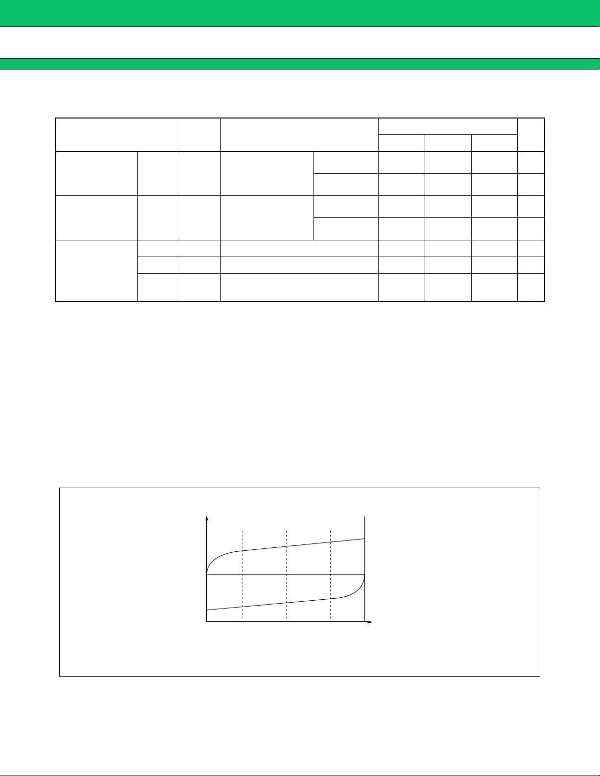
PIN DESCRIPTION
■
MB15F74UL
Pin no.
1fin
2Xfin
3GND
4VCCIF
Pin
name
I/O Descriptions
IF I
IF I
IF Ground pin for the IF-PLL section.
Prescaler input pin for the IF-PLL.
Connection to an external VCO should be AC coupling.
Prescaler complimentary input for the IF-PLL section.
This pin should be grounded via a capacitor.
Power supply voltage input pin for the IF-PLL section (except for the charge pump
circuit) , the shift register and the oscillator input buffer.
Power saving mode control pin for the IF-PLL section. This pin must be set at “L” when
5PS
6Vp
IF I
IF Power supply voltage input pin for the IF-PLL charge pump.
the power supply is started up. (Open is prohibited.)
PS
IF = “H” ; Normal mode/PSIF = “L” ; Power saving mode
7DoIF O Charge pump output for the IF-PLL section.
Lock detect signal output (LD) /phase comparator monitoring output (fout) pin. The
8 LD/fout O
output signal is selected by LDS bit in a serial data.
LDS bit = “H” ; outputs fout signal/LDS bit = “L” ; outputs LD signal
9Do
RF O Charge pump output for the RF-PLL section.
10 VpRF Power supply voltage input pin for the RF-PLL charge pump.
Power saving mode control for the RF-PLL section. This pin must be set at “L” when the
11 PS
RF I
power supply is started up. (Open is prohibited. )
PS
RF = “H” ; Normal mode/PSRF = “L” ; Power saving mode
12 V
13 GND
CCRF
RF Ground pin for the RF-PLL section
14 XfinRF I
15 fin
RF I
Power supply voltage input pin for the RF-PLL section (except for the charge pump
circuit)
Prescaler complimentary input pin for the RF-PLL section.
This pin should be grounded via a capacitor.
Prescaler input pin for the RF-PLL.
Connection to an external VCO should be via AC coupling.
Load enable signal input pin (with the schmitt trigger circuit)
16 LE I
When LE is set “H”, data in the shift register is transferred to the corresponding latch
according to the control bit in a serial data.
Serial data input pin (with the schmitt trigger circuit)
17 Data I
Data is transferred to the corresponding latch (IF-ref. counter, IF-prog. counter, RF-ref.
counter, RF-prog. counter) according to the control bit in a serial data.
18 Clock I
19 OSC
IN I
Clock input pin for the 23-bit shift register (with the schmitt trigger circuit)
One bit data is shifted into the shift register on a rising edge of the clock.
The programmable reference divider input pin. TCXO should be connected with an AC
coupling capacitor.
20 GND Ground pin for OSC input buffer and the shift register circuit.
3
Page 4
MB15F74UL
BLOCK DIAGRAM
■
PSIF
finIF
XfinIF
OSCIN
finRF
XfinRF
(5)
(1)
(2)
(19)
(15)
( )
14
Intermittent
mode control
(IF-PLL)
Prescaler
(IF-PLL)
(32/33, 64/65)
OR
Prescaler
(RF-PLL)
(64/65, 128/129)
3 bit latch
LDS
SWIF
7 bit latch 11 bit latch
Binary 7-bit
swallow counter
FCIF
(IF-PLL)
Binary 11-bit
programmable
counter (IF-PLL)
2 bit latch 14 bit latch 1 bit latch
T1 T2
Binary 14-bit pro-
grammable ref.
counter(IF-PLL)
C/P setting
counter
frIF
frRF
T1 T2
Binary 14-bit pro-
grammable ref.
counter (RF-PLL))
C/P setting
counter
2 bit latch 14 bit latch 1 bit latch
VCCIF GNDIF
(4)
fpIF
fpRF
(3)
Phase
comp.
(IF-PLL)
Lock Det.
Lock Det.
(IF-PLL)
LDIF
AND
LD
RF
(RF-PLL)
VpIF
(6)
Charge
pump
(IF-PLL)
Current
Switch
Fast
lock
Tuning
Selector
LD
frIF
frRF
fpIF
fpRF
(7)
(8)
DoIF
LD/
fout
PSRF
LE
Data
Clock
(11)
(16)
(17)
(18)
Intermittent
mode control
(RF-PLL)
Schmitt
circuit
Schmitt
circuit
Schmitt
circuit
Latch selector
C
C
N
N
23-bit shift register
1
2
LDS
SWRF
3 bit latch
Binary 7-bit
swallow counter
FCRF
(RF-PLL)
7 bit latch 11 bit latch
Binary 11-bit
programmable
counter (RF-PLL)
(20)
GND
Phase
comp.
(RF-PLL)
fpRF
(12) (13) (10)
V
CCRF
GNDRF
Tuning
Fast lock
Charge
pump
(RF-PLL)
VpRF
Current
Switch
(9)
DoRF
4
Page 5
ABSOLUTE MAXIMUM RATINGS
■
MB15F74UL
Parameter Symbol
Unit
Min Max
Rating
CC −0.5 4.0 V
V
Power supply voltage
Vp V
Input voltage V
I −0.5 VCC + 0.5 V
CC 4.0 V
LD/fout VO GND VCC V
Output voltage
Do
IF, DoRF VDO GND Vp V
Storage temperature Tstg −55 +125 °C
WARNING: Semiconductor devices can be permanently damaged by application of stress (voltage, current,
temperature, etc.) in excess of absolute maximum ratings. Do not exceed these ratings.
RECOMMENDED OPERATING CONDITIONS
■
Value
Parameter Symbol
Unit Remarks
Min Typ Max
V
CC 2.7 3.0 3.6 V VCCRF = VCCIF
Power supply voltage
Vp VCC 3.0 3.6 V
Input voltage V
I GND VCC V
Operating temperature Ta −40 +85 °C
Note : • VCCRF, VpRF, VCCIF and VpIF must supply equal voltage.
Even if either RF-PLL or IF-PLL is not used, power must be supplied to V
CCRF, VpRF, VCCIF and VpIF to keep
them equal.
It is recommended that the non-use PLL is controlled by power saving function.
• Although this device contains an anti-static element to prevent electrostatic breakdown and the circuitry
has been improved in electrostatic protection, observe the f ollowing precautions when handling the device .
• When storing and transporting the device, put it in a conductive case.
• Before handling the device, confirm the (jigs and) tools to be used hav e been uncharged (grounded) as
well as yourself. Use a conductive sheet on working bench.
• Before fitting the device into or removing it from the socket, turn the power supply off.
• When handling (such as transporting) the device mounted board, protect the leads with a conductiv e
sheet.
WARNING: The recommended operating conditions are required in order to ensure the normal operation of the
semiconductor device. All of the device’s electrical characteristics are warranted when the device is
operated within these ranges.
Always use semiconductor devices within their recommended operating condition ranges. Operation
outside these ranges may adversely affect reliability and could result in device failure.
No warranty is made with respect to uses, operating conditions, or combinations not represented on
the data sheet. Users considering application outside the listed conditions are advised to contact their
FUJITSU representatives beforehand.
5
Page 6
MB15F74UL
*
ELECTRICAL CHARACTERISTICS
■
(VCC = 2.7 V to 3.6 V, Ta = −40 °C to +85 °C)
Parameter Symbol Condition
Min Typ Max
CCIF
V
CCIF = VpIF = 3.0 V
2.1 2.5 3.2 mA
finIF = 2000 MHz
*1
I
Power supply current
CCRF
PSIF PSIF = PSRF = “L” 0.1
I
V
CCRF = VpRF = 3.0 V
5.7 6.5 8.4 mA
finRF = 2500 MHz
*1
I
Power saving current
IPSRF PSIF = PSRF = “L” 0.1
*3
fin
Operating frequency
fin
IF
RF
finIF IF PLL 200 2000 MHz
*3
finRF RF PLL 2000 4000 MHz
OSCIN fOSC 3 40 MHz
IF PfinIF IF PLL, 50 Ω system −15 +2dBm
fin
Input sensitivity
fin
RF PfinRF RF PLL, 50 Ω system −10 +2dBm
Input available voltage OSCIN VOSC 0.5 VCC VP−P
Value
*2
*2
Unit
10 µA
10 µA
“H” level input voltage
Data
VIH Schmitt trigger input
0.7 VCC
+ 0.4
V
LE
“L” level input voltage V
“H” level input voltage
“L” level input voltage VIL 0.3 VCC V
“H” level input current
Clock
PS
IF
PSRF
Data
IL Schmitt trigger input
VIH 0.7 VCC V
*4
IH
I
−1.0 +1.0 µA
0.3 VCC
− 0.4
LE
“L” level input current I
Clock
PS
“H” level input current
OSC
IN
“L” level input current IIL
“H” level output voltage
“L” level output voltage V
“H” level output voltage
“L” level output voltage V
High impedance cutoff
current
“H” level output current
“L” level output current I
LD/
fout
Do
DoRF
Do
DoRF
LD/
fout
IF
IF
*4
IL
−1.0 +1.0 µA
IIH 0 +100 µA
*4
V
OH VCC = Vp = 3.0 V, IOH = −1 mA VCC − 0.4 V
OL VCC = Vp = 3.0 V, IOL = 1 mA 0.4 V
−100 0 µA
VDOH VCC = Vp = 3.0 V, IDOH = −0.5 mA Vp − 0.4 V
DOL VCC = Vp = 3.0 V, IDOL = 0.5 mA 0.4 V
IOFF
IOH
VCC = Vp = 3.0 V
V
OFF = 0.5 V to Vp − 0.5 V
*4
VCC = Vp = 3.0 V −1.0 mA
OL VCC = Vp = 3.0 V 1.0 mA
2.5 nA
(Continued)
V
6
Page 7
(Continued)
Parameter Symbol Condition
MB15F74UL
(VCC = 2.7 V to 3.6 V, Ta = −40 °C to +85 °C)
Value
Unit
Min Typ Max
“H” level output
current
“L” level output
current
Charge pump
current rate
*8
IF
Do
DoRF
*8
IF
Do
DoRF
DOL/IDOH IDOMT
I
IDOH
IDOL
vs VDO IDOVD
vs Ta I
DOTA
VCC = Vp = 3.0 V,
*4
V
DOH = Vp / 2,
Ta = +25 °C
VCC = Vp = 3.0 V,
V
DOL = Vp / 2,
Ta = +25 °C
*5
VDO = Vp / 2 310%
*6
0.5 V ≤ VDO ≤ Vp − 0.5 V 10 15 %
−40 °C ≤ Ta ≤ 85 °C,
*7
V
DO = Vp / 2
CS bit = “H” −8.2 −6.0 −4.1 mA
CS bit = “L” −2.2 −1.5 −0.8 mA
CS bit = “H” 4.1 6.0 8.2 mA
CS bit = “L” 0.8 1.5 2.2 mA
510%
*1 : Conditions ; fosc = 12.8 MHz, Ta = +25 °C, SW = “L” in locking state.
CCIF = VpIF = VCCRF = VpRF = 3.0 V, fosc = 12.8 MHz, Ta = +25 °C, in power saving mode.
*2 : V
PS
IF = PSRF = GND
V
IH = VCC, VIL = GND (at CLK, Data, LE)
*3 : AC coupling. 1000 pF capacitor is connected under the condition of Min operating frequency.
*4 : The symbol “–” (minus) means the direction of current flow.
*5 : V
CC = Vp = 3.0 V, Ta = +25 °C (||I3| − |I4||) / [ (|I3| + |I4|) / 2] × 100 (%)
*6 : VCC = Vp = 3.0 V, Ta = +25 °C [ (||I2| − |I1||) / 2] / [ (|I1| + |I2|) / 2] × 100 (%) (Applied to both lDOL and lDOH)
*7 : V
CC = Vp = 3.0 V, [||IDO (+85 °C) | − |IDO (–40 °C) || / 2] / [|IDO (+85 °C) | + |IDO (–40 °C) | / 2] × 100 (%) (Applied to both
I
DOL and IDOH)
*8 : When Charge pump current is measured, set LDS = “L” , T1 = “L” and T2 = “H”.
I3
I2
I4
I1
IDOL
DOH
I
I1
I2
0.5 Vp/2 Vp − 0.5 Vp
Charge pump output voltage (V)
7
Page 8
MB15F74UL
FUNCTIONAL DESCRIPTION
■
1. Pulse swallow function
fVCO = [ (P × N) + A] × fOSC ÷ R
f
VCO : Output frequency of external voltage controlled oscillator (VCO)
P : Preset divide ratio of dual modulus prescaler (32 or 64 for IF-PLL, 64or 128 for RF-PLL)
N : Preset divide ratio of binary 11-bit programmable counter (3 to 2,047)
A : Preset divide ratio of binary 7-bit swallow counter (0 ≤ A ≤ 127, A < N)
f
OSC : Reference oscillation frequency (OSCIN input frequency)
R : Preset divide ratio of binary 14-bit programmable reference counter (3 to 16,383)
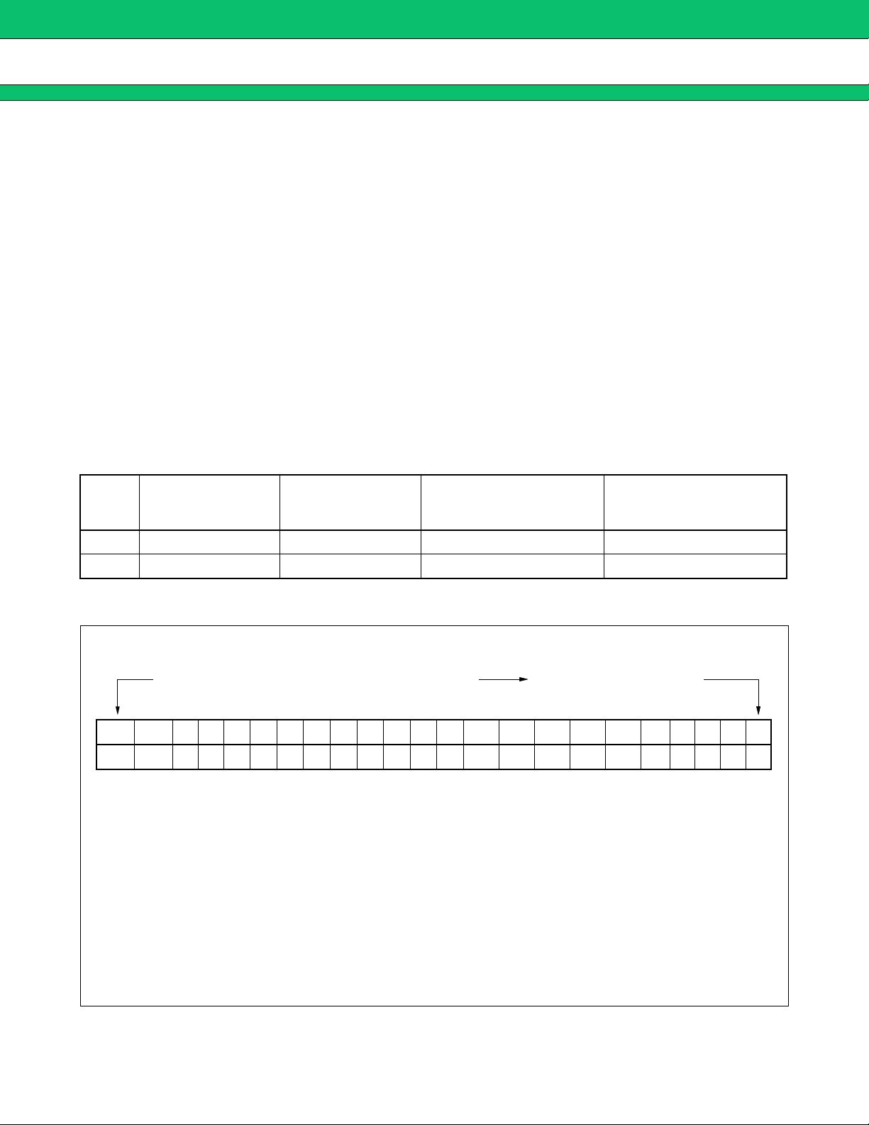
2. Serial Data Input
The serial data is entered using three pins, Data pin, Clock pin, and LE pin. Programmable dividers of IF/RFPLL sections, programmable reference dividers of IF/RF-PLL sections are controlled individually.
The serial data of binary data is entered through Data pin.
On rising edge of Clock, one bit of the serial data is transferred into the shift register. On a rising edge of load
enable signal, the data stored in the shift register is transf erred to one of latches depending upon the control bit
data setting.
The programmable
reference counter
for the IF-PLL
CN1 0 1 0 1
CN2 0 0 1 1
Shift Register Configuration
(1)
•
Programmable Reference Counter
(LSB)
1 2 3 4 5 6 7 8 9 10 11 12 13 14 15 16 17 18 19 20 21 22 23
CN1 CN2 T1 T2 R1 R2 R3 R4 R5 R6 R7 R8 R9 R10 R11 R12 R13 R14 CS X X X X
CS : Charge pump current select bit
R1 to R14 : Divide ratio setting bits for the programmable reference counter (3 to 16,383)
T1, 2 : LD/fout output setting bit
CN1, 2 : Control bit
X : Dummy bits (Set “0” or “1”)
The programmable
reference counter
for the RF-PLL
The programmable
counter and the swallow
counter for the IF-PLL
The programmable
counter and the swallow
counter for the RF-PLL
(MSB)Data Flow
Note : Data input with MSB first.
8
Page 9

MB15F74UL
• Programmable Counter
(LSB)
1 2 3 4 5 6 7 8 9 101112131415161718192021 22 23
SW
IF/
CN1 CN2 LDS
FCIF/
RF
A1 A2 A3 A4 A5 A6 A7
RF
A1 to A7 : Divide ratio setting bits for the swallow counter (0 to 127)
N1 to N11 : Divide ratio setting bits for the programmable counter (3 to 2,047)
LDS : LD/fout signal select bit
SW
IF/RF : Divide ratio setting bit for the prescaler (IF : SWIF, RF : SWRF)
FCIF/RF : Phase control bit for the phase detector (IF : FCIF, RF : FCRF)
CN1, 2 : Control bit
Note : Data input with MSB first.
Data Flow
(MSB)
N1 N2 N3 N4 N5 N6 N7 N8 N9 N10 N11
(2) Data setting
Binary 14-bit Programmable Reference Counter Data Setting
•
Divide ratio R14R13R12R11R10R9R8R7R6R5R4R3R2R1
3 00000000000011
4
•
•
•
16383
0
0
0
0
0
0
0
0
0
0
0
1
0
•
•
•
•
•
•
•
•
•
•
•
•
•
•
•
•
•
•
•
•
•
•
•
•
•
•
•
•
•
•
•
•
•
•
•
•
•
•
•
1
1
1
1
1
1
1
1
1
1
1
1
1
Note : Divide ratio less than 3 is prohibited.
•
Binary 11-bit Programmable Counter Data Setting
Divide ratioN11N10N9N8N7N6N5N4N3N2N1
3 00000000011
4
•
•
•
2047
0
0
0
0
0
0
0
0
1
0
0
•
•
•
•
•
•
•
•
•
•
•
•
•
•
•
•
•
•
•
•
•
•
•
•
•
•
•
•
•
•
•
•
•
1
1
1
1
1
1
1
1
1
1
1
Note : Divide ratio less than 3 is prohibited
•
Binary 7-bit Swallow Counter Data Setting
Divide ratioA7A6A5A4A3A2A1
0 0000000
1
•
•
•
127
0
0
0
0
0
0
1
•
•
•
•
•
•
•
•
•
•
•
•
•
•
•
•
•
•
•
•
•
1
1
1
1
1
1
1
0
•
•
•
1
9
Page 10

MB15F74UL
• Prescaler Data Setting
Divide ratio SW
====
“H” SW
Prescaler divide ratio IF-PLL 32/33 64/65
Prescaler divide ratio RF-PLL 64/65 128/129
• Charge Pump Current Setting
Current value CS
±6.0 mA 1
±1.5 mA 0
•
LD/fout output Selectable Bit Setting
LD/fout pin state LDS T1 T2
000
LD output
010
011
====
“L”
IF 100
fr
fout
output
frRF 110
fp
IF 101
fp
RF 111
• Phase Comparator Phase Switching Data Setting
====
IF, RF
FC
“H” FCIF, RF
Phase comparator input
IF, RF
Do
fr > fp H L
fr < fp L H
fr = fp Z Z
Z
: High-impedance
Depending upon the VCO and LPF polarity, FC bit should be set.
(1) VCO polarity FC = “H”
(2) VCO polarity FC = “L”
VCO Output
Frequency
DoIF,
High
====
RF
“L”
(1)
Note : Give attention to the polarity for using active type LPF.
10
LPF Output voltage
(2)
Max
Page 11

MB15F74UL
3. Power Saving Mode (Intermittent Mode Control Circuit)
Status PS pin
Normal mode
Power saving mode
The intermittent mode control circuit reduces the PLL power consumption.
By setting the PS pin low, the device enters into the po wer saving mode, reducing the current consumption. See
the Electrical Characteristics chart for the specific value.
The phase detector output, Do, becomes high impedance.
For the dual PLL, the lock detector, LD, is as shown in the LD Output Logic table.
Setting the PS pin high, releases the power saving mode, and the device works normally.
The intermittent mode control circuit also ensures a smooth startup when the device returns to normal operation.
When the PLL is returned to normal operation, the phase comparator output signal is unpredictable. This is
because of the unknown relationship between the comparison frequency (fp) and the reference frequency (fr)
which can cause a major change in the comparaor output, resulting in a VCO frequency jump and an increase
in lockup time.
H
L
To prevent a major VCO frequency jump, the intermittent mode control circuit limits the magnitude of the error
signal from the phase detector when it returns to normal operation.
Notes : • When power (VCC) is first applied, the device must be in standby mode.
• PS pin must be set “L” at Power-ON.
ONOFF
VCC
Clock
Data
LE
PS
(1) (2) (3)
tV ≥ 1 µs
tPS ≥ 100 ns
(1) PS = L (power saving mode) at Power-ON
(2) Set serial data at least 1 µs after the power supply becomes stable (V
(3) Release power saving mode (PS
IF, PSRF : “L” → “H”) at least 100 ns later after setting serial data.
CC ≥ 2.2 V) .
11
Page 12

MB15F74UL
4. Serial Data Data Input Timing
Divide ratio is performed through a serial interface using the Data pin, Clock pin, and LE pin.
Setting data is read into the shift register at the rise of the Clock signal, and transferred to a latch at the rise of
the LE signal. The following diagram shows the data input timing.
1st data 2nd data
Invalid data
t6
t4 t5
Data
Clock
LE
Control bit
LSBMSB
t1 t2 t3
t7
Parameter Min Typ Max Unit Parameter Min Typ Max Unit
t
1 20 ns t5 100 ns
t
2 20 ns t6 20 ns
t
3 30 ns t7 100 ns
12
t
4 30 ns
Note : LE should be “L” when the data is transferred into the shift register.
Page 13

PHASE COMPARATOR OUTPUT WAVEFORM
■
frIF/RF
fpIF/RF
tWU tWL
LD
(FC bit = High)
DoIF/RF
Z
H
MB15F74UL
L
(FC bit = Low)
DoIF/RF
Z
L
H
• LD Output Logic
IF-PLL section RF-PLL section LD output
Locking state/Power saving state Locking state/Power saving state H
Locking state/Power saving state Unlocking state L
Unlocking state Locking state/Power saving state L
Unlocking state Unlocking state L
Notes : • Phase error detection range = −2π to +2π
• Pulses on Do
• LD output becomes low when phase error is t
• LD output becomes high when phase error is t
• t
WU and tWL depend on OSCIN input frequency as follows.
t
WU ≥ 2/fosc : e.g. tWU ≥ 156.3 ns when fosc = 12.8 MHz
t
WU ≤ 4/fosc : e.g. tWL ≤ 312.5 ns when fosc = 12.8 MHz
IF/RF signals during locking state are output to prevent dead zone.
WU or more.
WL or less and continues to be so for three cycles or more.
13
Page 14
MB15F74UL
TEST CIRCUIT (for Measuring Input Sensitivity fin/OSC
■
S.G.
1000 pF
S.G.
1000 pF
50 Ω
finIF
XfinIF
GNDIF
VCCIF
PSIF
VpIF
1000 pF
50 Ω
GND OSCIN DataClock
20
1
2
3
4
5
6
MB15F74UL
7
19
17
109
16
15
14
13
12
11
18
8
)
IN
Controller
(Divide ratio setting)
1000 pF
LE
fin
RF
XfinRF
GNDRF
VCCRF
PSRF
VCCRF
S.G.
50 Ω
1000 pF
VCCIF
0.1 µF
Oscilloscope
VpIF
0.1 µF
LD/foutDoIF DoRF VpRF
VpRF
0.1 µF
0.1 µF
14
Page 15

TYPICAL CHARACTERISTICS
■
1.
fin input sensitivity
10
0
−10
−20
PfinRF [dBm]
−30
−40
RF-PLL input sensitivity vs. Input frequency
SPEC
MB15F74UL
VCC = 2.7 V
V
CC = 3.0 V
V
CC = 3.6 V
SPEC
−50
1000 1500 2000 2500 3000 3500 4000 4500 5000 5500 6000
finRF [MHz]
IF-PLL input sensitivity vs. Input frequency
10
0
SPEC
−10
−20
PfinIF [dBm]
−30
−40
−50
0 500 1000 1500 2000 2500 3000 3500
finIF [MHz]
CC = 2.7 V
V
CC = 3.0 V
V
VCC = 3.6 V
SPEC
15
Page 16

MB15F74UL
2.
OSCIN input sensitivity
10
SPEC
0
−10
−20
−30
−40
Input sensitivity VOSC (dBm)
−50
0 50 100 150 200 250 300
Input sensitivity vs. Input frequency
VCC = 2.7 V
V
CC = 3.0 V
V
CC = 3.6 V
SPEC
Input
frequency fOSC (MHz)
16
Page 17

3. RF-PLL Do output current
• 1.5 mA mode
MB15F74UL
IDO − VDO
10.0
VCC = Vp = 3.0 V
0
• 6.0 mA mode
Charge pump output current IDO (mA)
−10.0
1.0 3.00.0 2.0
Charge pump output voltage VDO (V)
I
DO − VDO
10.0
VCC = Vp = 3.0 V
0
Charge pump output current IDO (mA)
−10.0
0.0 2.0
1.0 3.0
Charge pump output voltage VDO (V)
17
Page 18

MB15F74UL
4.
IF-PLL Do output current
• 1.5 mA mode
Charge pump output current IDO (mA)
IDO − VDO
10.0
−10.0
VCC = Vp = 3.0 V
0
0.0 2.0
1.0 3.0
Charge pump output voltage VDO (V)
• 6.0 mA mode
Charge pump output current IDO (mA)
IDO − VDO
10.0
VCC = Vp = 3.0 V
0
−10.0
0.0 2.0
1.0 3.0
Charge pump output voltage VDO (V)
18
Page 19

5.
fin input impedance
finIF input impedance
4
: 16.453 Ω−46.539 Ω
MB15F74UL
2 000.000 000 MHz
866.25
1
:
916.31
−
100 MHz
76.5
2
:
319.2
−
500 MHz
31.078
3
:
152.46
−
1 GHz
1
2
Ω
Ω
Ω
Ω
Ω
Ω
4
START 100.000 000 MHz STOP 2 000.000 000 MHz
RF input impedance
fin
4
: 25.791 Ω 34.824 Ω
4
3
3
4 000.000 000 MHz
1
35 336
:
−
2
:
−
3
:
743.16 m
−
151.85
1 GHz
17.436
52.191
2 GHz
20.211
3 GHz
Ω
Ω
Ω
Ω
Ω
Ω
1
2
START 1 000.000 000 MHz STOP 4 000.000 000 MHz
19
Page 20

MB15F74UL
6. OSC
IN
input impedance
OSCIN input impedance
4
: 049.5 Ω−1.0414 kΩ
100.000 000 MHz
15.882 k
1
:
11.652 k
−
3 MHz
3.924 k
2
:
8.942 k
−
10 MHz
286
3
:
2.5913 k
−
4
40 MHz
1
2
3
Ω
Ω
Ω
Ω
Ω
Ω
START 3.000 000 MHz STOP 100.000 000 MHz
20
Page 21

REFERENCE INFORMATION
■
(for Lock-up Time, Phase Noise and Reference Leakage)
Test Circuit
S.G.
Spectrum
Analyzer
OSC
fin
IN
Do
VCO
LPF
• PLL Reference Leakage
fVCO = 2500 MHz
KV = 50 MHz/V
fr = 200 kHz
f
OSC = 13 MHz
LPF
1500 pF
MB15F74UL
CC = 3.0 V
V
Ta = + 25 °C
CP : 6 mA mode
7.5 k
Ω
2.7 kΩ
15000 pF
To VCO
330 pF
• PLL Phase Noise
ATTEN 10 dB
RL 0 dBm
∆MKR
200 kHz
D
−70.00 dB
S
CENTER 2.500000 GHz
∗
RBW 3.0 kHz VBW 3.0 kHz
ATTEN 10 dB
RL 0 dBm
∆MKR
1.00 kHz
D
−69.01 dB/Hz
S
∆MKR −70.00 dB
200 kHz10 dB/
SPAN 1.000 MHz
SWP 280 ms
∆MKR −69.01 dB
1.00 kHz10 dB/
CENTER 2.50000000 GHz
∗
RBW 30 Hz VBW 30 Hz
SPAN 10.00 kHz
SWP 1.92 s
(Continued)
21
Page 22

MB15F74UL
(Continued)
2500 MHz→2550 MHz within ± 1 kHz
L ch→H ch 440 µs
A Mkr x: 439.99764 µs
y: 50.0009 MHz
100.0050
MHz
2.00
kHz/div
99.99500
MHz
0 s
PLL Lock Up time
2.0000000 ms
PLL Lock Up time
2550 MHz→2500 MHz within ± 1 kHz
H ch→L ch 400 µs
A Mkr x: 400.00146 µs
y: −50.0013 MHz
100.0050
MHz
2.00
kHz/div
99.99500
MHz
0 s
2.0000000 ms
22
Page 23

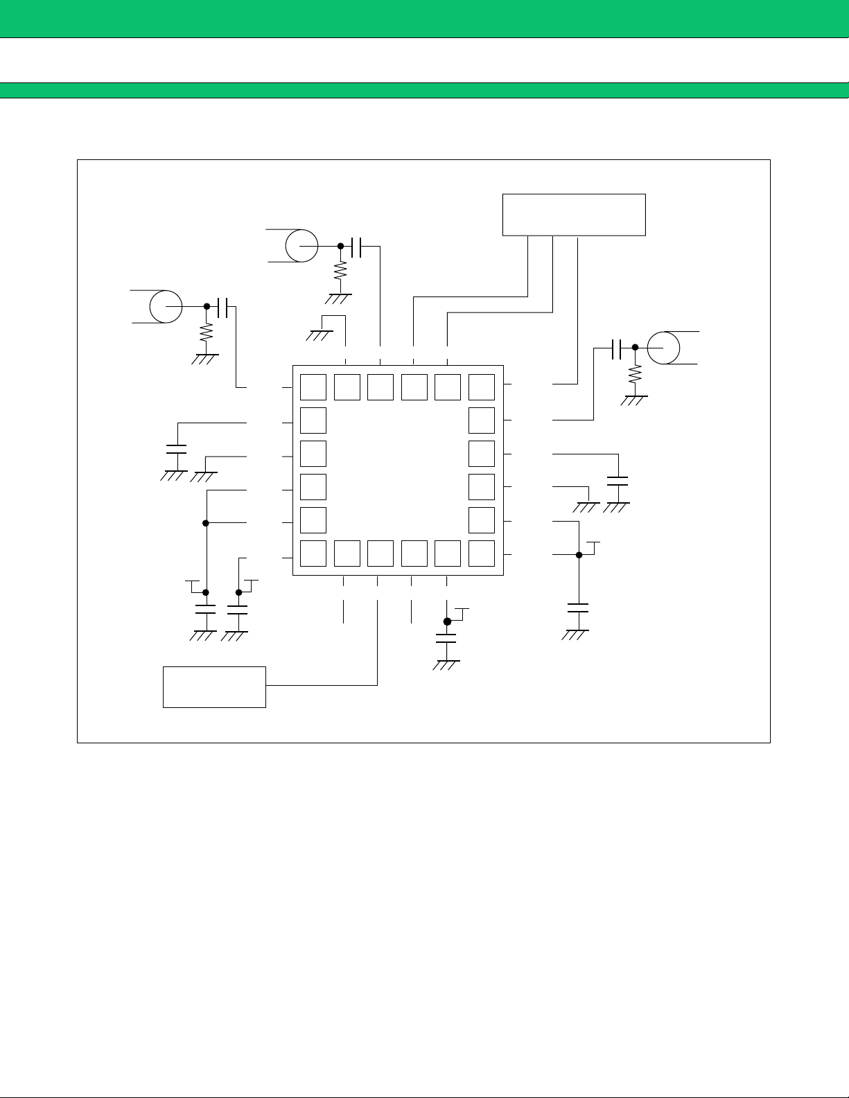
APPLICATION EXAMPLE
■
1000 pF
TCXO
finIF
XfinIF
1000 pF
GND OSCIN DataClock
20
1
2
19
18
17
16
15
LE
fin
MB15F74UL
From controller
1000 pF
RF
1000 pF
3.0 V
0.1 µF
GNDIF
VCCIF
PSIF
VpIF
3.0 V
0.1 µF
3
4
5
6
MB15F74UL
8
7
LD/foutDoIF DoRF VpRF
Lock Det.
14
13
12
109
11
3.0 V
0.1 µF
LPF VCO
LPF VCO
XfinRF
GNDRF
VCCRF
PSRF
1000 pF
3.0 V
0.1 µF
Output
Output
Note : Clock, Data, LE : The schmitt trigger circuit is provided (insert a pull-down or pull-up register
to prevent oscillation when open-circuit in the input) .
23
Page 24

MB15F74UL
USAGE PRECAUTIONS
■
(1) VCCRF, VpRF, VCCIF and VpIF must be equal voltage.
Even if either RF-PLL or IF-PLL is not used, power must be supplied to V
them equal. It is recommended that the non-use PLL is controlled by power saving function.
(2) To protect against damage by electrostatic discharge, note the following handling precautions :
• Store and transport devices in conductive containers.
• Use properly grounded workstations, tools, and equipment.
• Turn off power before inserting or removing this device into or from a socket.
• Protect leads with conductive sheet, when transporting a board mounted device
ORDERING INFORMATION
■
Part number Package Remarks
MB15F74ULPVA
20-pad plastic BCC
(LCC-20P-M05)
CCRF, VpRF, VCCIF and VpIF to keep
24
Page 25

PACKAGE DIMENSION
■
20-pad plastic BCC
(LCC-20P-M05)
MB15F74UL
3.60±0.10(.142±.004)
1116
INDEX AREA
16
0.05(.002)
3.40±0.10
(.134±.004)
Details of "A" part
0.50±0.10
(.020±.004)
(.024±.004)
0.60±0.10
0.55±0.05
(.022±.002)
(Mounting height)
2.70(.106)
0.075±0.025
(.003±.001)
(Stand off)
Details of "B" part
0.50±0.10
(.020±.004)
0.25±0.10
(.010±.004)
TYP
0.30±0.10
(.012±.004)
3.00(.118)TYP
0.25±0.10
(.010±.004)
11 16
"D"
"B""A" "C"
0.50(.020)
TYP
2.80(.110)REF
Details of "C" part
0.50±0.10
(.020±.004)
C0.20(.008)
0.60±0.10
(.024±.004)
Details of "D" part
0.30±0.10
(.012±.004)
0.50(.020)
TYP
16
0.40±0.10
(.016±.004)
C
2001 FUJITSU LIMITED C20056S-c-2-1
Dimensions in mm (inches
)
25
Page 26

MB15F74UL
FUJITSU LIMITED
All Rights Reserved.
The contents of this document are subject to change without notice.
Customers are advised to consult with FUJITSU sales
representatives before ordering.
The information and circuit diagrams in this document are
presented as examples of semiconductor device applications, and
are not intended to be incorporated in devices for actual use. Also,
FUJITSU is unable to assume responsibility for infringement of
any patent rights or other rights of third parties arising from the use
of this information or circuit diagrams.
The products described in this document are designed, developed
and manufactured as contemplated for general use, including
without limitation, ordinary industrial use, general office use,
personal use, and household use, but are not designed, developed
and manufactured as contemplated (1) for use accompanying fatal
risks or dangers that, unless extremely high safety is secured, could
have a serious effect to the public, and could lead directly to death,
personal injury, severe physical damage or other loss (i.e., nuclear
reaction control in nuclear facility, aircraft flight control, air traffic
control, mass transport control, medical life support system, missile
launch control in weapon system), or (2) for use requiring
extremely high reliability (i.e., submersible repeater and artificial
satellite).
Please note that Fujitsu will not be liable against you and/or any
third party for any claims or damages arising in connection with
above-mentioned uses of the products.
Any semiconductor devices have an inherent chance of failure. You
must protect against injury, damage or loss from such failures by
incorporating safety design measures into your facility and
equipment such as redundancy, fire protection, and prevention of
over-current levels and other abnormal operating conditions.
If any products described in this document represent goods or
technologies subject to certain restrictions on export under the
Foreign Exchange and Foreign Trade Law of Japan, the prior
authorization by Japanese government will be required for export
of those products from Japan.
F0210
FUJITSU LIMITED Printed in Japan
 Loading...