

Page 1
FUJITSU SEMICONDUCTOR
DATA SHEET
ASSP
Single Serial Input
PLL Frequency Synthesizer
On-chip 2.5 GHz Prescaler
MB15E07SL
DESCRIPTION
■■■■
The Fujitsu MB15E07SL is a serial input Phase Locked Loop (PLL) frequency synthesizer with a 2.5 GHz prescaler .
The 2.5 GHz prescaler has a dual modulus division ratio of 32/33 or 64/65 enabling pulse s wallowing operation.
The supply voltage range is between 2.4 V and 3.6 V. The MB15E07SL uses the latest BiCMOS process, as a
result the supply current is typically 3.5 mA at 2.7 V. A refined charge pump supplies well-balanced output currents
of 1.5 mA and 6 mA. The charge pump current is selectable by serial data.
MB15E07SL is ideally suited for wireless mobile communications, such as GSM (Global System for Mobile
Communications) and PCS.
DS04-21358-4E
FEATURES
■■■■
• High frequency operation: 2.5 GHz Max
• Low power supply voltage: VCC = 2.4 to 3.6 V
• Ultra Low power supply current:I
• Direct power saving function: Power supply current in power saving mode
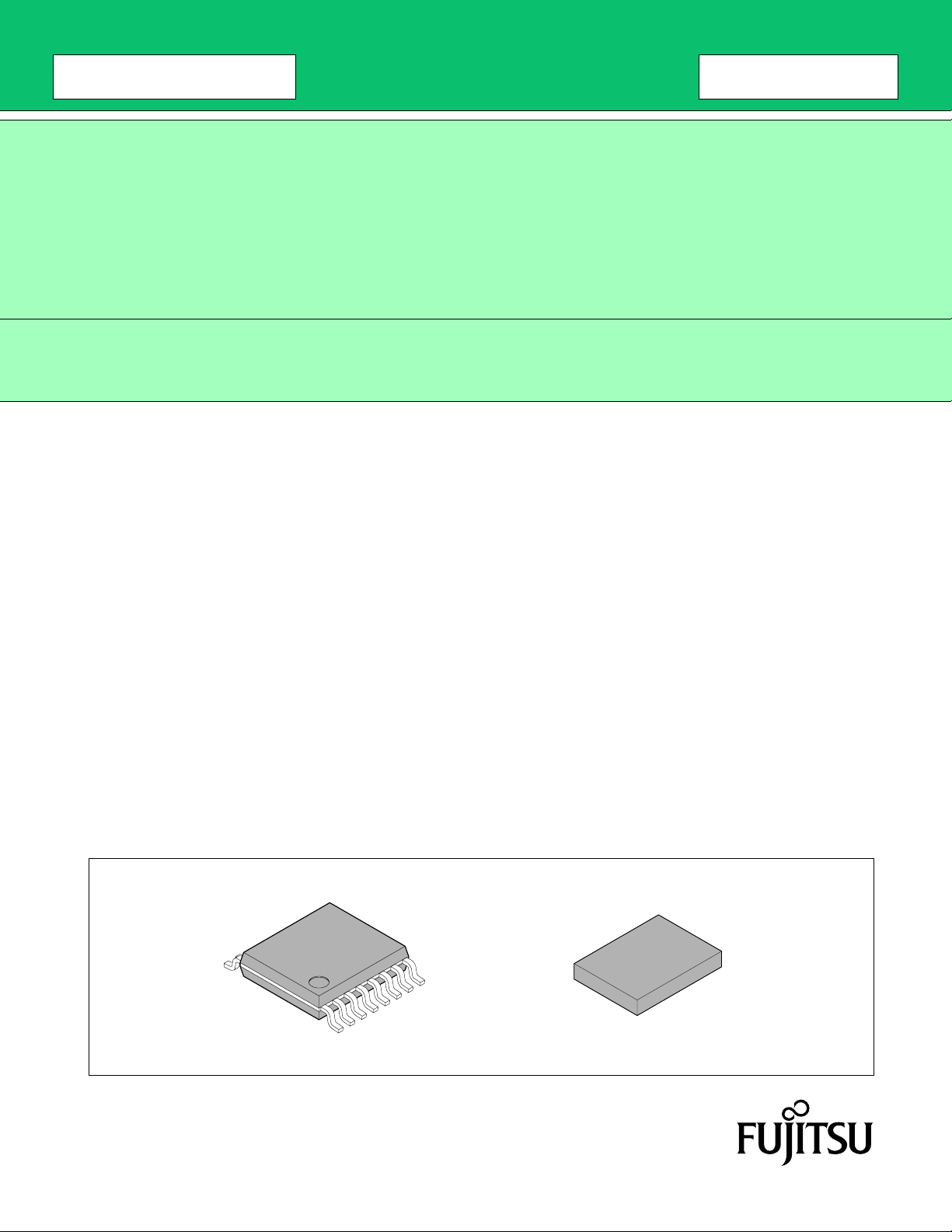
PACKAGES
■■■■
16-pin plastic SSOP
(FPT-16P-M05)
CC = 3.5 mA Typ (VCC = Vp = 2.7 V, Ta = +25°C, in locking state)
ICC = 4.0 mA Typ (VCC = Vp = 3.0 V, Ta = +25°C, in locking state)
Typ 0.1 µA (V
CC = Vp = 3.0 V, Ta = +25°C), Max 10 µA (VCC = Vp = 3.0 V)
(Continued)
16-pad plastic BCC
(LCC-16P-M06)
Page 2
MB15E07SL
(Continued)
• Dual modulus prescaler: 32/33 or 64/65
• Serial input 14-bit programmable reference divider: R = 3 to 16,383
• Serial input programmable divider consisting of:
- Binary 7-bit swallow counter: 0 to 127
- Binary 11-bit programmable counter: 3 to 2,047
• Software selectable charge pump current
• On-chip phase control for phase comparator
• Operating temperature: Ta = –40 to +85°C
• Pin compatible with MB15E07, MB15E07L
PIN ASSIGNMENTS
■
16-pin SSOP 16-pad BCC
OSCIN
OSCOUT
VP
VCC
DO
GND
Xfin
fin
1
2
3
4
Top view
5
6
7
8
16
15
14
13
12
11
10
9
(FPT-16P-M05)
φR
φP
LD/fout
ZC
PS
LE
Data
Clock
OSC
OUT
VP
VCC
DO
GND
Xfin
(LCC-16P-M06)
IN φR
OSC
1
2
3
Top view
4
5
678 9
fin Clock
141516
13
12
11
10
φP
LD/fout
ZC
PS
LE
Data
2
Page 3
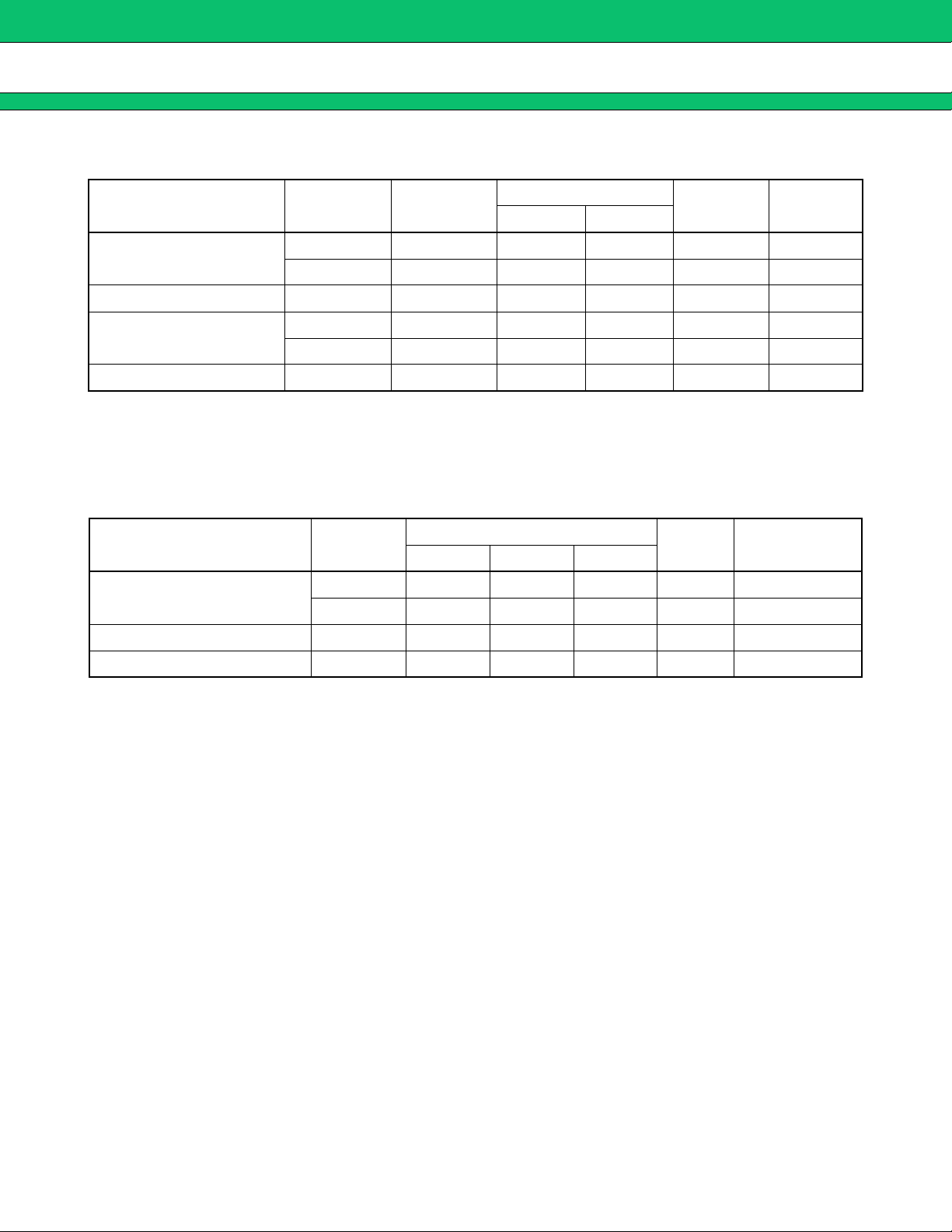
PIN DESCRIPTIONS
■
MB15E07SL
Pin no.
SSOP BCC
116OSC
21OSC
32V
Pin
name
OUT O Oscillator output.
P – Power supply voltage input for the charge pump.
I/O Descriptions
IN I Programmable reference divider input. Connection to a TCXO.
43VCC – Power supply voltage input.
54D
O O
Charge pump output.
Phase of the charge pump can be selected via programming of the FC bit.
6 5 GND – Ground.
7 6 Xfin I Prescaler complementary input, which should be grounded via a capacitor.
87finI
Prescaler input.
Connection to an external VCO should be done via AC coupling.
Clock input for the 19-bit shift register.
98ClockI
Data is shifted into the shift register on the rising edge of the clock.
(Open is prohibited.)
10 9 Data I
Serial data input using binary code.
The last bit of the data is a control bit. (Open is prohibited.)
Load enable signal input. (Open is prohibited.)
11 10 LE I
When LE is set high, the data in the shift register is transferred to a latch
according to the control bit in the serial data.
Power saving mode control. This pin must be set at “L” at Power-ON.
12 11 PS I
(Open is prohibited.)
PS = “H”; Normal mode
PS = “L”; Power saving mode
Forced high-impedance control for the charge pump (with internal pull up
13 12 ZC I
resistor.)
ZC = “H”; Normal Do output.
ZC = “L”; Do becomes high impedance.
Lock detect signal output (LD)/phase comparator monitoring output (fout).
14 13 LD/fout O
The output signal is selected via programming of the LDS bit.
LDS = “H”; outputs fout (fr/fp monitoring output)
LDS = “L”; outputs LD (“H” at locking, “L” at unlocking.)
15 14 φPO
16 15 φRO
Phase comparator N-channel open drain output for an external charge
pump. Phase can be selected via programming of the FC bit.
Phase comparator CMOS output for an external charge pump. Phase can
be selected via programming of the FC bit.
3
Page 4
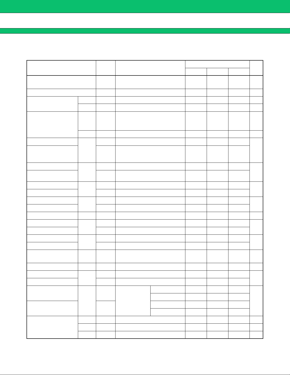
MB15E07SL
BLOCK DIAGRAM
■
OSCIN
OSC
V
OUT
VP
D
(16)
1
(1)
2
(2)
3
(3)
4
CC
(4)
O
5
Reference
oscillator
circuit
Charge pump
Current switch
Binary 14-bit
reference counter
14-bit latch
. .
C
N
T
19-bit shift register
. . .
7-bit latch
Binary 7-bit
swallow counter
SW FC CS
LDS
4-bit latch
. . .
11-bit latch
Binary 11-bit
programmable
counter
fr
Phase
comparator
Lock
detector
LD/fr/fp
fp
selector
Intermittent
mode control
(power save)
(15)
16
(14)
15
(13)
14
(12)
13
(11)
12
φR
φP
LD/fout
ZC
PS
(10)
11
(9)
10
(8)
98
LE
Data
Clock
GND
Xfin
fin
(5)
6
(6)
7
(7)
: SSOP
( ) : BCC
1-bit
control
latch
MD
Prescaler
32/33
64/65
4
Page 5
ABSOLUTE MAXIMUM RATINGS
■
MB15E07SL
Parameter Symbol Condition
Unit Remark
Min Max
Rating
V
CC ––0.54.0V
Power supply voltage
V
P –VCC 6.0 V
Input voltage V
I ––0.5VCC +0.5 V
VO Except Do GND VCC V
Output voltage
V
O Do GND VP V
Storage temperature Tstg – –55 +125 °C
WARNING: Semiconductor devices can be permanently damaged by application of stress (voltage, current,
temperature, etc.) in excess of absolute maximum ratings. Do not exceed these ratings.
RECOMMENDED OPERATING CONDITIONS
■
Value
Parameter Symbol
Unit Remark
Min Typ Max
V
CC 2.4 3.0 3.6 V
Power supply voltage
V
P VCC –5.5V
Input voltage VI GND – VCC V
Operating temperature Ta –40 – +85 °C
WARNING: The recommended operating conditions are required in order to ensure the normal operation of the
semiconductor device. All of the device’s electrical characteristics are warranted when the device is
operated within these ranges.
Always use semiconductor devices within their recommended operating condition ranges. Operation
outside these ranges may adversely affect reliability and could result in device failure.
No warranty is made with respect to uses, operating conditions, or combinations not represented on
the data sheet. Users considering application outside the listed conditions are advised to contact their
FUJITSU representatives beforehand.
5
Page 6
MB15E07SL
ELECTRICAL CHARACTERISTICS
■
(VCC = 2.4 to 3.6 V, Ta = –40 to +85°C)
Parameter Symbol Condition
Min Typ Max
Power supply current*
1
Power saving current I
ICC
fin = 2500 MHz, VCC = VP = 2.7 V
*1
(V
CC = VP = 3.0 V)
PS ZC = “H” or open – 0.1
–
fin fIN – 700 – 2500 MHz
Operating frequency
OSCIN OSCIN –3–40MHz
50 Ω system
*3
Input sensitivity
fin
OSC
“H” level input voltage Data,
Pfin
(Refer to the measurement
–15 – +2 dBm
circuit.)
*3
IN
VOSC –0.5–VCC Vp-p
VIH –VCC × 0.7 – –
Clock,
“L” level input voltage V
LE, PS,
IL –––VCC × 0.3
ZC
“H” level input current Data,
“L” level input current IIL
Clock,
LE, PS
“H” level input current
OSC
“L” level input current IIL
IN
“H” level input current
“L” level input current IIL
ZC
“L” level output voltage φφφφPV
“H” level output voltage
“L” level output voltage VOL VCC = VP = 3.0 V, IOL = 1 mA – – 0.4
“H” level output voltage
φφφφR,
LD/fout
Do
*4
I
IH
*4
––1.0–+1.0
––1.0–+1.0
IIH – 0 – +100
*4
*4
I
IH
*4
Pull up input –100 – 0
OL Open drain output – – 0.4 V
––100–0
––1.0–+1.0
VOH VCC = VP = 3.0 V, IOH = –1 mA VCC – 0.4 – –
V
DOH VCC = VP = 3.0 V, IDOH = –0.5 mA VP – 0.4 – –
“L” level output voltage VDOL VCC = VP = 3.0 V, IDOL = 0.5 mA – – 0.4
High impedance cutoff
current
Do I
“L” level output current φφφφPI
“H” level output current
“L” level output current IOL –1.0––
“H” level output current
φφφφR,
LD/fout
I
DOH
Do
“L” level output current IDOL
I
DOL/IDOH IDOMT
Charge pump current
rate
vs V
DO IDOVD
vs Ta IDOTA
VCC = VP = 3.0 V,
OFF
V
OFF = 0.5 V to VP – 0.5 V
OL Open drain output 1.0 – – mA
––2.5nA
IOH ––––1.0
*4
VCC = 3 V,
V
P = 3 V,
V
DO = VP/2
Ta = +25°C
*5
VDO = VP/2 –3–%
*6
0.5 V ≤ VDO ≤ VP – 0.5 V – 10 – %
*7
– 40°C ≤ Ta ≤ +85°C–10–%
CS bit = “H” – –6.0 –
CS bit = “L” – –1.5 –
CS bit = “H” – 6.0 –
CS bit = “L” – 1.5 –
Value
3.5
(4.0)
*2
Unit
–mA
10 µA
V
µA
µA
µA
V
V
mA
mA
*1 : Conditions; fosc = 12 MHz, Ta = +25°C, in locking state.
CC = VP = 3.0 V, fosc = 12.8 MHz, Ta = +25°C, in power saving mode
*2 : V
6
Page 7

MB15E07SL
*3 : AC coupling. 1000 pF capacitor is connected under the condition of Min operating frequency.
*4 : The symbol “–” (minus) means direction of current flow.
CC = VP = 3.0 V, Ta = +25°C (|I3| – |I4|) / [(|I3| + |I4|) /2] × 100(%)
*5 : V
*6 : VCC = VP = 3.0 V, Ta = +25°C [(|I2| – |I1|) /2] / [(|I1| + |I2|) /2] × 100(%) (Applied to each IDOL, IDOH)
CC = VP = 3.0 V, VDO = VP/2 (|IDO(85°C) – IDO(–40°C)| /2) / (|IDO(85°C) + IDO(–40°C)| /2) × 100(%) (Applied to each IDOL, IDOH)
*7 : V
IDOL
IDOH
I1
I2
0.5
Charge Pump Output Voltage (V)
I3
I2
I4
I1
Vp/2VpVp − 0.5 V
7
Page 8
MB15E07SL
FUNCTIONAL DESCRIPTION
■
1. Pulse Swallow Function
The divide ratio can be calculated using the following equation:
fVCO = [(M × N) + A] × fOSC ÷ R (A < N)
f
VCO : Output frequency of external voltage controlled oscillator (VCO)
N : Preset divide ratio of binary 11-bit programmable counter (3 to 2,047)
A : Preset divide ratio of binary 7-bit swallow counter (0 ≤ A ≤ 127)
f
OSC : Output frequency of the reference frequency oscillator
R : Preset divide ratio of binary 14-bit programmable reference counter (3 to 16,383)
M : Preset divide ratio of modulus prescaler (32 or 64)
2. Serial Data Input
Serial data is processed using the Data, Clock, and LE pins. Serial data controls the programmable reference
divider and the programmable divider separately.
Binary serial data is entered through the Data pin.
One bit of data is shifted into the shift register on the rising edge of the Clock. When the LE signal pin is taken
high, stored data is latched according to the control bit data as follows:
Table 1. Control Bit
Control bit (CNT) Destination of serial data
H For the programmable reference divider
L For the programmable divider
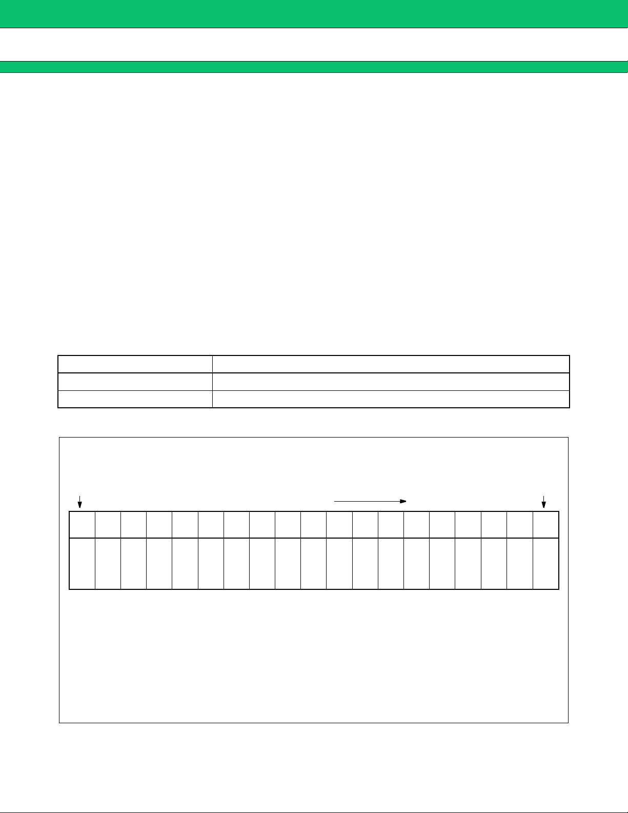
(1) Shift Register Configuration
Programmable Reference Counter
LSB
Data Flow
12345678910111213141516171819
C
R1R2R3R4R5R6R7R8R9R10R11R12R13R
N
T
CNT : Control bit [Table 1]
R1 to R14 : Divide ratio setting bit for the programmable reference counter (3 to 16,383) [Table 2]
SW : Divide ratio setting bit for the prescaler (32/33 or 64/65) [Table 5]
FC : Phase control bit for the phase comparator [Table 8]
LDS : LD/f
CS : Charge pump current select bit [Table 6]
OUT signal select bit [Table 7]
14 SW FC LDS CS
MSB
Note: Start data input with MSB first.
8
Page 9

Programmable Counter
MB15E07SL
LSB
1234567891 0111 21 31 41 51 61 71 81 9
C
A1A2A3A4A5A6A7N1N2N3N4N5N6N7N8N9N10N
N
T
CNT : Control bit [Table 1]
N1 to N11 : Divide ratio setting bits for the programmable counter (3 to 2,047) [Table 3]
A1 to A7 : Divide ratio setting bits for the swallow counter (0 to 127) [Table 4]
Note: Data input with MSB first.
Table 2. Binary 14-bit Programmable Reference Counter Data Setting
Divide ratio (R) R14 R13 R12 R11 R10 R9 R8 R7 R6 R5 R4 R3 R2 R1
3 00000000000011
4 00000000000100
⋅ ⋅⋅⋅⋅⋅⋅⋅⋅⋅⋅⋅⋅⋅⋅
16383 11111111111111
Data Flow
11
MSB
Note : Divide ratio less than 3 is prohibited.
Table 3. Binary 11-bit Programmable Counter Data Setting
Divide ratio (N)N11N10N9N8N7N6N5N4N3N2N1
3 00000000011
4 00000000100
⋅ ⋅⋅⋅⋅⋅⋅⋅⋅⋅⋅⋅
2047 11111111111
Note : Divide ratio less than 3 is prohibited.
Table 4. Binary 7-bit Swallow Counter Data Setting
Divide ratio (A) A7A6A5A4A3A2A1
0 0000000
1 0000001
⋅ ⋅⋅⋅⋅⋅⋅⋅
127 1111111
9
Page 10

MB15E07SL
Table 5. Prescaler Data Setting
SW Prescaler divide ratio
H32/33
L64/65
Table 6. Charge Pump Current Setting
CS Current value
H ±6.0 mA
L ±1.5 mA
Table 7. LD/fout Output Select Data Setting
LDS
H fout signal
L LD signal
LD/
OUT
f
output signal
(2) Relation between the FC Input and Phase Characteristics
The FC bit changes the phase characteristics of the phase comparator. Both the internal charge pump output
level (D
(f
O) and the phase comparator output (φR, φP) are re v ersed according to the FC bit. Also, the monitor pin
OUT) output is controlled by the FC bit. The relationship between the FC bit and each of DO, φR, and φP is shown
below .
Table 8. FC Bit Data Setting (LDS = “H”)
FC = High FC = Low
O φ
D
fr > f
P HLL
P LHZ* HLL
fr = f
P Z* L Z* Z* L Z*
φ
R
φφ
φφφφ
PLD/foutD
O φ
φ
R
φφ
φφφφ
PLD/fout
LHZ*
fout = fr
fout = fpfr < f
* : High-Z
10
Page 11

MB15E07SL
When designing a synthesizer, the FC pin setting depends on the VCO and LPF characteristics.
* : When the LPF and VCO characteristics are similar
to (1), set FC bit high.
* : When the VCO characteristics are similar to (2), set
FC bit low.
VCO
Output
PLL LPF VCO
3. Do Output Control
Table 9. ZC Pin Setting
ZC pin Do output
H Normal output
Frequency
LPF Output Voltage
(1)
(2)
L High impedance
4. Power Saving Mode (Intermittent Mode Control Circuit)
Table 10. PS Pin Setting
PS pin Status
H Normal mode
L Power saving mode
The intermittent mode control circuit reduces the PLL power consumption.
By setting the PS pin low , the de vice enters into the power sa ving mode, reducing the current consumption. See
the Electrical Characteristics chart for the specific value.
The phase detector output, Do, becomes high impedance.
For the signal PLL, the lock detector, LD, remains high, indicating a locked condition.
Setting the PS pin high, releases the power saving mode, and the device works nor mally.
The intermittent mode control circuit also ensures a smooth startup when the device returns to normal operation.
When the PLL is returned to normal operation, the phase comparator output signal is unpredictable. This is
because
of the unknown relationship between the comparison frequency (fp) and the reference frequency (fr) which can
cause a major change in the comparator output, resulting in a VCO frequency jump and an increase in lockup
time.
To prevent a major VCO frequency jump, the intermittent mode control circuit limits the magnitude of the error
signal from the phase detector when it returns to normal operation.
When power (V
CC) is first applied, the device must be in standby mode, PS = Low, for at least 1 µs.
11
Page 12

MB15E07SL
Note : PS pin must be set “L” for Power-ON
V
CC
Clock
Data
LE
PS
(1) (2) (3)
(1) PS = L (power saving mode) at Power ON
(2) Set serial data 1 µs later after power supply remains stable (V
(3) Release power saving mode (PS: L → H) 100 ns later after setting serial data.
.
ONOFF
tV ≥ 1 µs
≥
t
PS
100 ns
CC > 2.2 V).
12
Page 13

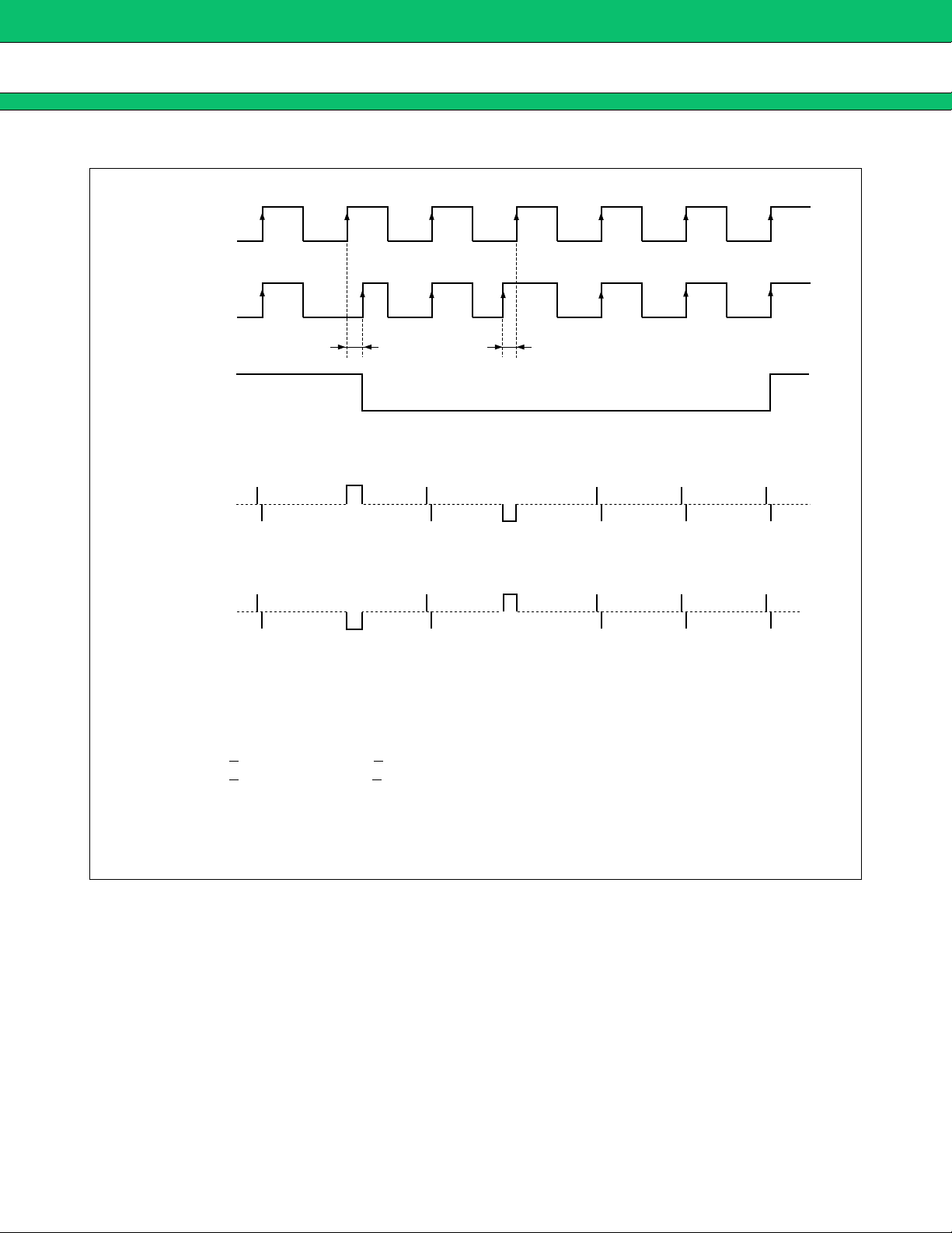
SERIAL DATA INPUT TIMING
■
MB15E07SL
Data
Clock
LE
1st data
Control bit Invalid data
∼
MSB LSB
∼
∼
t
1 t2 t3
t7
∼
On the rising edge of the clock, one bit of data is transferred into the shift register.
Parameter Min Typ Max Unit
t
1 20 – – ns
t
2 20 – – ns
t3 30 – – ns
Parameter Min Typ Max Unit
t
5 100 – – ns
t
6 20 – – ns
t7 100 – – ns
t4 30 – – ns
2nd data
t6
t5t4
Note : LE should be “L” when the data is transferred into the shift register.
13
Page 14
MB15E07SL
PHASE COMPARATOR OUTPUT WAVEFORM
■
fr
fp
tWU tWL
LD
[FC = “H”]
DO
[FC = “L”]
DO
Notes : • Phase error detection range: –2π to +2π
• Pulses on Do signal during locked state are output to prevent dead zone.
• LD output becomes low when phase is t
is t
WL or less and continues to be so for three cycles or more.
• t
WU and tWL depend on OSCIN input frequency.
t
WU > 2/fosc (s) (e. g. tWU > 156.3 ns, fosc = 12.8 MHz)
t
WU < 4/fosc (s) (e. g. tWL < 312.5 ns, fosc = 12.8 MHz)
• LD becomes high during the power saving mode (PS = “L”).
WU or more. LD output becomes high when phase error
14
Page 15

MB15E07SL
MEASURMENT CIRCUIT (for Measuring Input Sensitivity fin/OSC
■
1000 pF
S • G
1000 pF
50 Ω
Controller (setting divide ratio)
fin Xfin GND DO VCC VP OSCOUT OSCIN
86431
9101112 14
Clock Data LE
0.1 µF
75 2
13 15 16
PS ZC LD/fout
VCC
0.1 µF
φP φR
1000 pF
Note: SSOP-16
50 Ω
)
IN
S • G
Oscilloscope
15
Page 16

MB15E07SL
■ TYPICAL CHARACTERISTICS
1. fin input sensitivity
Input sensitivity − Input frequency (Prescaler: 64/65)
10
0
−10
−20
−30
Input sensitivity Pfin (dBm)
−40
−50
0 200 400 600 800 1000 1200 1400 1600 1800 2000 2200 2400 2600 2800 3000
Input frequency fin (MHz)
Input sensitivity − Input frequency (Prescaler: 32/33)
10
0
−10
SPEC
SPEC
VCC = 2.4 V
V
CC = 3.0 V
V
CC = 3.6 V
Ta = +25 °C
Ta = +25 °C
16
−20
−30
−40
Input sensitivity Pfin (dBm)
−50
0 200 400 600 800 1000 1200 1400 1600 1800 2000 2200 2400 2600 2800 3000
Input frequency fin (MHz)
VCC = 2.7 V
V
CC = 3.0 V
V
CC = 3.6 V
Page 17

2. OSCIN input sensitivity
MB15E07SL
Input sensitivity − Input frequency
10
0
−10
−20
−30
−40
Input sensitivity VOSC (dBm)
−50
−60
0 50 100 150 200
SPEC
Input frequency f
OSC (MHz)
Ta = +25 °C
VCC = 2.4 V
V
CC = 3.0 V
V
CC = 3.6 V
17
Page 18

MB15E07SL
3. Do output current
1.5 mA mode
VDO - IDO
Charge pump output current IDO (mA)
10.00
2.000
/div
–10.00
0
0
Ta = +25°C
VCC = 3.0 V
Vp = 3.0 V
IDOL
I
DOH
.6000/div
Charge pump output voltage VDO (V)
4.800
6.0 mA mode
Charge pump output current IDO (mA)
10.00
2.000
/div
–10.00
0
0
Ta = +25°C
V
CC = 3.0 V
Vp = 3.0 V
VDO - IDO
IDOL
I
DOH
.6000/div
Charge pump output voltage VDO (V)
4.800
18
Page 19

4. fin input impedance
MB15E07SL
12.646
1
:
–57.156
2
:
–12.136
4
3
:
4 :
3
2
1 GHz
22.156
1.5 GHz
33.805
11.869
2 GHz
23.715 Ω
8.9629 Ω
2.5 GHz
Ω
Ω
Ω
Ω
Ω
Ω
5. OSC
START 500.000 000 MHz STOP 2 500.000 000 MHz
IN
input impedance
1
9.917
4
3
2
1
1
:
2
:
3
:
–3.4046
4 :
–3.643
3 MHz
3.7903
–4.812
10 MHz
1.574
20 MHz
453.12 Ω
–1.9213 Ω
40 MHz
Ω
Ω
Ω
Ω
Ω
Ω
START 1.000 000 MHz STOP 50.000 000 MHz
19
Page 20
MB15E07SL
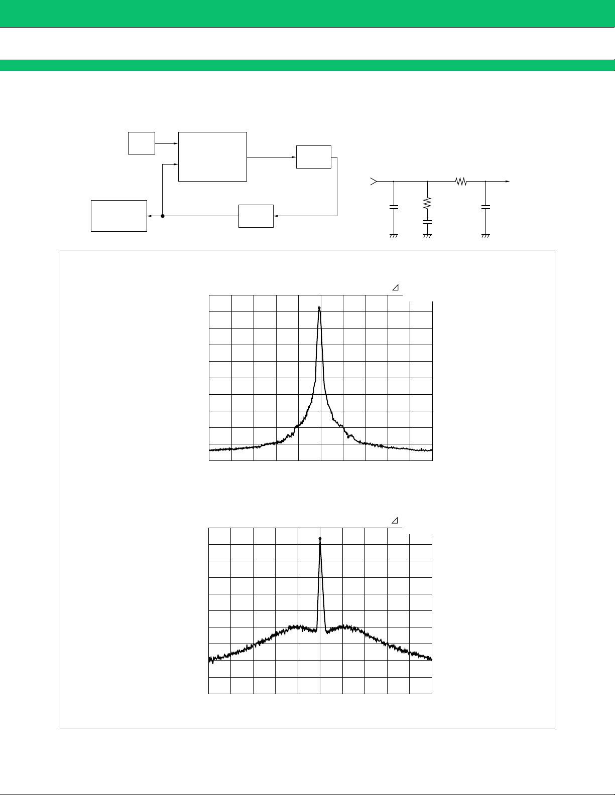
■ REFERENCE INFORMATION
S.G
Spectrum
Analyzer
PLL Reference Leakage
Test Circuit
OSCIN
fin
REF –5.0 dBm
10 dB/
RBW
1 kHz
SAMPLE
VBW
1 kHz
Do
VCO
ATT 10 dB
LPF
fVCO = 810.45 MHz
K
V = 17 MHz/V
fr = 25 kHz
fOSC = 14.4 MHz
LPF
4700 pF
MKR
25.0 kHz
–78.0 dB
CC =VP = 3.0 V
V
V
VCO = 2.3 V
Ta = +25 °C
CP : 6 mA mode
9.1 kΩ
4.2 kΩ
0.047 µF
1500 pF
PLL Phase Noise
SWP 1.0 s
REF –5.0 dBm
10 dB/
RBW
100 Hz
SAMPLE
VBW
100 Hz
SWP 10 s
SPAN 200 kHz
ATT 10 dB
SPAN 20.0 kHz
CENTER 810.000 MHz
MKR
CENTER 810.000 MHz
2.28 kHz
–53.1 dB
(Continued)
20
Page 21

(Continued)
810 MH→826 MHz within ± 1 kHz
Lch→Hch 1.30 ms
MB15E07SL
PLL Lock Up time PLL Lock Up time
826 MH→810 MHz within ± 1 kHz
Hch→Lch 1.28 ms
846.000 MHz
826.000 MHz
806.000 MHz
826.004000 MHz
826.000000 MHz
825.996000 MHz
500.0 µs/div
500.0 µs/div
838.000 MHz
818.000 MHz
798.000 MHz
500.0 µs/div
810.004000MHz
810.000000MHz
809.996000MHz
500.0 µs/div
21
Page 22

MB15E07SL
■■■■ APPLICATION EXAMPLE
VP
10 kΩ
12 kΩ
12 kΩ
10 kΩ
Lock Det.
φR φP
16 15 14 13 12 11 10 9
LD/fout
ZC Clock
MB15E07SL
PS
LPF
LE Data
VCO
OUTPUT
From
a controller
22
123 4 5678
OSCIN
TCXO
OSCOUT
1000 pF
VP: 5.5 V Max
Notes : • SSOP-16
• In case of using a crystal resonator, it is necessary to optimize matching between the crystal
and this LSI, and perform detailed system evaluation. It is recommended to consult with a
supplier of the crystal resonator. (Reference oscillator circuit pro vides its own bias, f eedback
resistor is 100 kΩ (Typ).)
VP
0.1 µF
VCC
0.1 µF
DO
GND
Xfin
1000 pF
fin
1000 pF
Page 23

MB15E07SL
USAGE PRECAUTIONS
■
To protect against damage by electrostatic discharge, note the following handling precautions:
-Store and transport devices in conductive containers.
-Use properly grounded workstations, tools, and equipment.
-Turn off power before inserting device into or removing device from a socket.
-Protect leads with a conductive sheet when transporting a board-mounted device.
ORDERING INFORMATION
■
Part number Package Remarks
MB15E07SLPFV1
MB15E07SLPV1
16-pin, Plastic SSOP
(FPT-16P-M05)
16-pad, Plastic BCC
(LCC-16P-M06)
23
Page 24

MB15E07SL
■■■■ PACKAGE DIMENSIONS
16-pin plastic SSOP
(FPT-16P-M05)
1
*
5.00±0.10(.197±.004)
16
INDEX
LEAD No.
1 8
0.65(.026)
9
2
*
4.40±0.10 6.40±0.20
0.24±0.08
(.009±.003)
Note 1) *1 : Resin protrusion. (Each side : +0.15 (.006) Max).
Note 2) *2 : These dimensions do not include resin protrusion.
Note 3) Pins width and pins thickness include plating thickness.
Note 4) Pins width do not include tie bar cutting remainder.
0.17±0.03
(.007±.001)
(.252±.008)(.173±.004)
Details of "A" part
+0.20
–0.10
1.25
(Mounting height)
+.008
.049
–.004
"A"
0.13(.005)
M
0~8˚
0.10(.004)
C
2003 FUJITSU LIMITED F16013S-c-4-6
0.50±0.20
(.020±.008)
0.60±0.15
(.024±.006)
Dimensions in mm (inches
0.10±0.10
(.004±.004)
0.25(.010)
)
(Stand off)
Note : The values in parentheses are reference values.
(Continued)
24
Page 25

(Continued)
16-pad plastic BCC
(LCC-16P-M06)
MB15E07SL
4.55±0.10
(.179±.004)
INDEX AREA
1 6
0.05(.002)
C
1999 FUJITSU LIMITED C16017S-1C-1
0.80(.031)MAX
Mounting height
3.40±0.10
(.134±.004)
0.075±0.025
(.003±.001)
(Stand off)
3.40(.134)TYP
0.65(.026)
0.40±0.10
(.016±.004)
0.80(.031)
REF
2.45(.096)
TYP
Details of "A" part
9
6
0.75±0.10
(.030±.004)
0.40±0.10
(.016±.004)
TYP
"A"
Dimensions in mm (inches
0.325±0.10
(.013±.004)
"B"
1.725(.068)
REF
Details of "B" part
0.60±0.10
(.024±.004)
)
0.60±0.10
(.024±.004)
14914
1
1.15(.045)
REF
Note : The values in parentheses are reference values.
25
Page 26

MB15E07SL
FUJITSU LIMITED
All Rights Reserved.
The contents of this document are subject to change without notice.
Customers are advised to consult with FUJITSU sales
representatives before ordering.
The information, such as descriptions of function and application
circuit examples, in this document are presented solely for the
purpose of reference to show examples of operations and uses of
Fujitsu semiconductor device; Fujitsu does not warrant proper
operation of the device with respect to use based on such
information. When you develop equipment incorporating the
device based on such information, you must assume any
responsibility arising out of such use of the information. Fujitsu
assumes no liability for any damages whatsoever arising out of
the use of the information.
Any information in this document, including descriptions of
function and schematic diagrams, shall not be construed as license
of the use or exercise of any intellectual property right, such as
patent right or copyright, or any other right of Fujitsu or any third
party or does Fujitsu warrant non-infringement of any third-party’s
intellectual property right or other right by using such information.
Fujitsu assumes no liability for any infringement of the intellectual
property rights or other rights of third parties which would result
from the use of information contained herein.
The products described in this document are designed, developed
and manufactured as contemplated for general use, including
without limitation, ordinary industrial use, general office use,
personal use, and household use, but are not designed, developed
and manufactured as contemplated (1) for use accompanying fatal
risks or dangers that, unless extremely high safety is secured, could
have a serious effect to the public, and could lead directly to death,
personal injury, severe physical damage or other loss (i.e., nuclear
reaction control in nuclear facility, aircraft flight control, air traffic
control, mass transport control, medical life support system, missile
launch control in weapon system), or (2) for use requiring
extremely high reliability (i.e., submersible repeater and artificial
satellite).
Please note that Fujitsu will not be liable against you and/or any
third party for any claims or damages arising in connection with
above-mentioned uses of the products.
Any semiconductor devices have an inherent chance of failure. You
must protect against injury, damage or loss from such failures by
incorporating safety design measures into your facility and
equipment such as redundancy, fire protection, and prevention of
over-current levels and other abnormal operating conditions.
If any products described in this document represent goods or
technologies subject to certain restrictions on export under the
Foreign Exchange and Foreign Trade Law of Japan, the prior
authorization by Japanese government will be required for export
of those products from Japan.
F0306
FUJITSU LIMITED Printed in Japan
 Loading...