

Page 1

FUJITSU MICROELECTRONICS
DATA SHEET
DS04–21348–3Ea
ASSP
Single Serial Input
PLL Frequency Synthesizer
On-Chip prescaler
MB15C02
■ DESCRIPTION
The Fujitsu Microelectronics MB15C02 is a serial input Phase Locked Loop (PLL) frequency synthesizer with a
prescaler. A 64/65 division is available for the prescaler that enables pulse swallow operation.
This operates with a supply voltage of 1.0 V (min.).
MB15C02 is suitable for mobile communications, such as paging systems.
■ FEATURES
• High frequency operation: 220 MHz max @VDD = 1.0 V to 1.5 V
330 MHz max @V
450 MHz max @V
• Single power supply : V
• Power saving function
• Pulse swallow function: 64/65
• Serial input 14-bit programmable reference divider: R = 5 to 16,383
• Serial input 18-bit programmable divider consisting of:
- Binary 6-bit swallow counter: 0 to 63
- Binary 12-bit programmable counte r: 5 to 4,0 95
• Wide operating temperature: Ta = –20 to 60°C
■ PACKAGES
16-pin, Plastic SSOP
DD = 1.0 to 1.5 V
DD = 1.2 V to 1.5 V
DD = 1.3 V to 1.5 V
20-pin, Plastic SSOP
(FPT-16P-M05)
Copyright©1999-2008 FUJITSU MICROELECTRONICS LIMITED All rights reserved
1999.2
(FPT-20P-M03)
1
Page 2

MB15C02
■ PIN ASSIGNMENTS
SSOP-20 pin
SSOP-16 pin
VDD
Clock
NC
Data
LE
fin
PS
NC
LD
Do
V
1
2
3
4
5
6
7
8
9
10
(FPT-20P-M03)
DD
1
Top
View
20
19
18
17
16
15
14
13
12
11
16
VSS
OSC
IN
NC
OSCOUT
TEST
FC
φP
NC
φR
Vp
VSS
Clock
Data
LE
fin
PS
LD
Do
2
3
4
5
6
7
8
Top
View
15
14
13
12
11
10
OSC
IN
OSCOUT
TEST
FC
φP
φR
Vp
9
(FPT-16P-M05)
2
Page 3

■ PIN DESCRIPTIONS
MB15C02
Pin no.
SSOP16SSOP
20
1 1 VDD – Power supply voltage
2 2 Clock I
– 3 NC – No connection
3 4 Data I Serial data input using binary code.(Schmitt trigger input)
4 5 LE I
5 6 fin I
6 7 PS I
– 8 NC – No connection
7 9 LD O
8 10 Do O
9 11 Vp – Power supply for the charge pump.
10 12 φR O
– 13 NC – No connection
11 14 φP O
12 15 FC I Phase comparator input select pin.
13 16 TEST I
Pin
name
I/O Descriptions
Clock input for the shift register.(Schmitt trigger input)
Data is shifted into the shift register on the rising edge of the clock.
Load enable signal input (Schmitt trigger input)
When LE is high, the data in the shift register is transferred to a latch,
according to the control bit in the serial data.
Prescaler input.
A bias circuit and amplifier are at input port. Connection with an external
VCO should be done by AC coupling.
Power saving mode control. This pin must be set at “L” at Power-ON.
PS = “H” ; Normal mode
PS = “L” ; Power saving mode
Lock detector signal output.
When a PLL is locking, LD outputs “H”.
When a PLL is not locking, LD outputs “L”.
Charge pump output.
Phase of the charge pump can be reversed by FC input. The Do output
may be inverted by FC input. The relationships between the programmable
reference divider out put (fr) and the programmable divider output (fp) are
shown below;
fr > fp :“H” level (FC = “L”), “L” level (FC = “H”)
fr = fp : High impedance
fr < fp :“L” level (FC = “L”), “H” level (FC = “H”)
Phase comparator output pin (for external charge pump). Relation between
the programmabl e ref erence divider output ( fr) and the prog rammab le divider
output (fp) are shown below;
When FC = “L”
fr > fp : φR = “L” level, φP = “L” level
fr = fp : φR = “L” level, φP = High impedance
fr < fp : φR = “H” level, φP = High impedance
When FC = “H”
fr > fp : φR = “H” level, φP = High impedance
fr = fp : φR = “L” level, φP = High impedance
fr < fp : φR = “L” level, φP = “L” level
Phase comparator output pin (for external charge pump). Refer to Pin
description for φR. φP pin is a Nch open drain output.
Test mode select pin. (Pull down resistor)
Please set this pin to ground or open usually.
(Continued)
3
Page 4

MB15C02
(Continued)
Pin no.
SSOP16SSOP
20
14 17 OSCOUT O
– 18 NC – No connection
15 19 OSCIN I
16 20 VSS – Ground pin.
Pin
name
I/O Descriptions
Oscillator output.
Connection for an external crystal.
Programmable reference divider input.
Oscillator input.
Clock can be input to OSC
pin open and make connection with OSC
IN from outside. In the case, please leave OSCOUT
IN as AC coupling.
4
Page 5
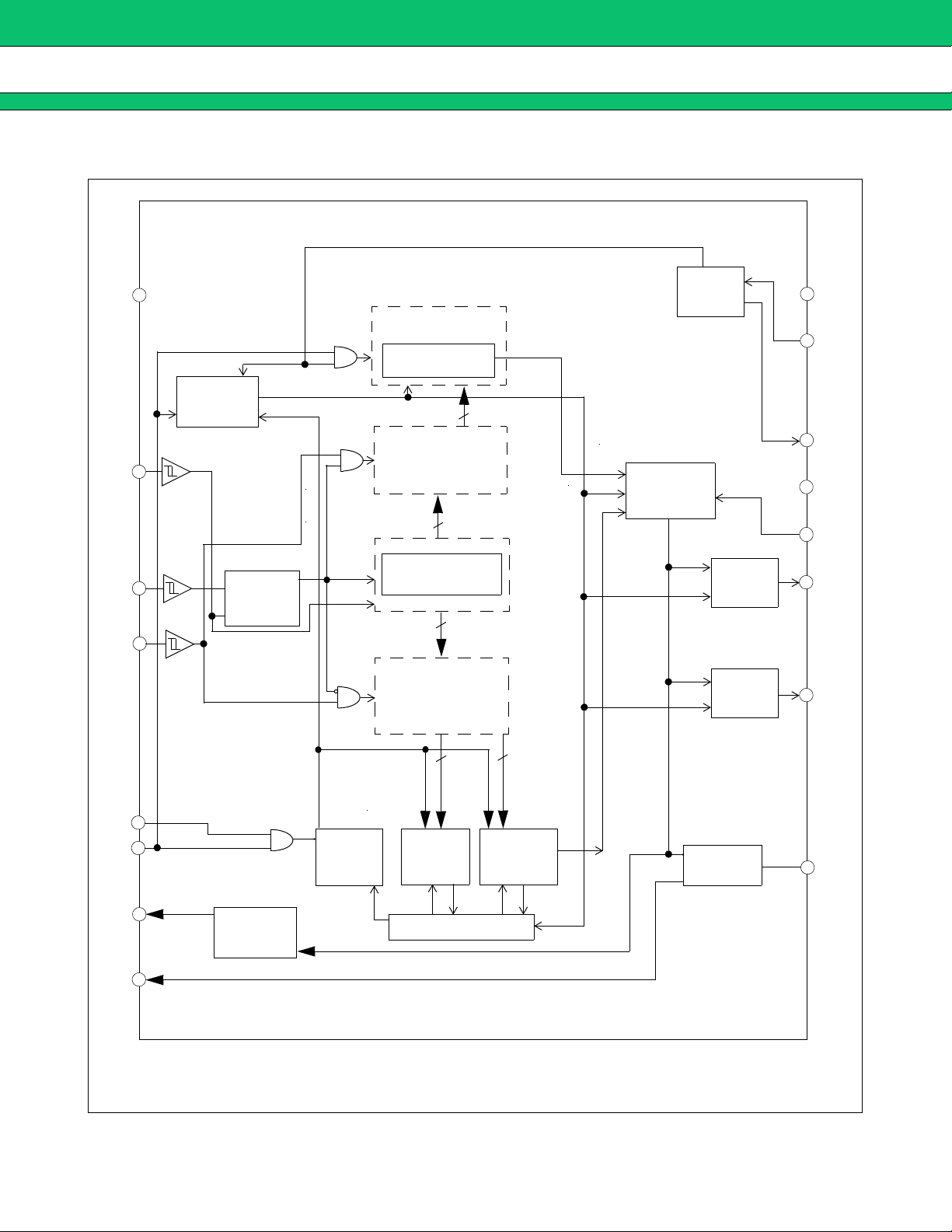
■ BLOCK DIAGRAM
VDD
Intermittent
mode control
circuit
Clock
Programmable
reference divider
Binary 14-bit
reference counter
14-bit latch
14
14
fr
fp
oscillator
Phase
comparator
MB15C02
Crystal
VSS
circuit
OSCIN
OSCOUT
TEST
FC
Data
LE
PS
LD
Do
18-bit shift register
Control
register
18
18-bit latch
6
fin
Binary 6-bit
Prescaler
Lock detector
swallow
counter
Control circuit
12
Binary 12-bit
programma-
ble counter
Output
control
circuit
Output
control
circuit
Charge
pump
φP
φR
VP
5
Page 6
MB15C02
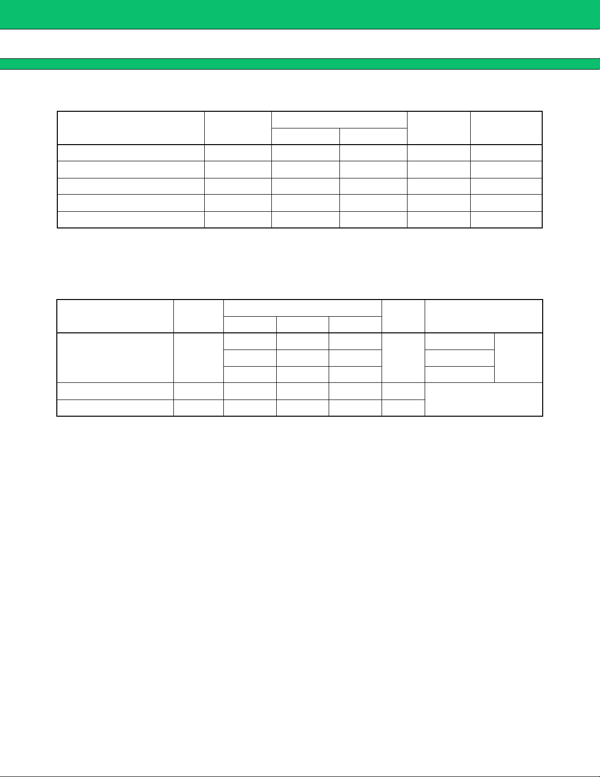
■ ABSOLUTE MAXIMUM RATINGS
Parameter Symbol
Unit Remark
Min. Max.
Rating
Power supply voltage V
Input voltage V
Output voltage V
Output current I
Storage temperature T
DD, VP GND–0.5 +2.0 V
IN GND–0.5 VDD +0.5 V
OUT GND–0.5 VDD +0.5 V
OUT –10 +10 mA
stg –40 +125 °C
WARNING: Semiconductor devices can be permanently damaged by application of stress (voltage, current,
temperature, etc.) in excess of absolute maximum ratings. Do not exceed these ratings.
■ RECOMMENDED OPERATING CONDITIONS
Parameter Symbol
Power supply voltage V
DD, VP
Input voltage V
Min. Typ. Max.
1.0 – 1.5
1.3 – 1.5 For 450 MHz
IN GND – VDD V
Value
Unit Remark
For 220 MHz
V
V
DD = VP1.2 – 1.5 For 330 MHz
Operating temperature Ta –20 – +60 °C
WARNING: The recommended operating conditions are required in order to ensure the normal operation of the
semiconductor device. All of the device’s electrical characteristics are warranted when the device is
operated within these ranges.
Always use semiconductor de vi ces with in their reco mmended oper ating condition ra nges . Oper ation
outside these ranges may adversely affect reliability and could result in device failure.
No warranty is made with respect to uses, operating conditions, or combinat ions not represented on
the data sheet. Users considering application outside the listed conditio ns are advised to contact their
representatives beforehand.
6
Page 7

■ ELECTRICAL CHARACTERISTICS
MB15C02
(For 220 MHz :VDD = Vp = 1.0 to 1.5 V, Ta = –20 to +60°C)
(For 330 MHz :V
(For 450 MHz :V
DD = Vp = 1.2 to 1.5 V, Ta = –20 to +60°C)
DD = Vp = 1.3 to 1.5 V, Ta = –20 to +60°C)
Parameter Symbol Condition
Power supply current Active Mode
Power saving current
Power saving mode
fin fin
Operating frequency
IN fOSC
OSC
fin Vfin AC coupling –2.0 – – dBm
Input sensitivity
OSCin V
Input voltage
Input current
Output voltage
Except for
fin and
OSCin
Except for
fin, OSCin
and TEST
Except for
OSC
OUT
and φP
H level V
L level V
H level I
L level I
H level V
L level V
Value
Unit
*4
mA
µA
I
I
DDS
DD
(VDD=1.0V/220MHz)
*1
(V
DD=1.2V/330MHz)
(V
DD=1.3V/450MHz)
(VDD=1.0V)
*2
(VDD=1.2V)
(V
DD=1.3V)
Min.
–
–
–
–
–
–
Typ.
0.6
1.0
1.3
50
70
80
*3
Max.
1.2
1.8
2.2
250
300
350
Programmable divider
DD=1.0 to 1.5V)
(V
(V
DD=1.2 to 1.5V)
(V
DD=1.3 to 1.5V)
Programmable
reference divider
OSC AC coupling –2.0 – – dBm
IH –
IL ––– 0.2
IH VIN=VDD ––+1.0
10
10
10
5–20MHz
DD –
V
0.2
–
–
–
220
330
450
MHz
––
V
µA
IL VIN=GND –1.0 – –
DD –
OH IOH = –0.2 mA
OL IOL = 0.2 mA – – 0.2
V
0.2
––
V
φPL levelV
High impedance
cutoff current
Do I
φPI
*1: Conditions; Inputs except for fin, OSC
Specifying the current flowing in V
OFF1 VOUT = GND to VP –100 – 100 nA
OFF2 VOUT = VDD ––100nA
IN and TEST are grounded, Outputs are opened.
DD and Vp at operating state under conditions of VDD = Vp, fin =
220 MHz, or 330 MHz, and OSCIN = 12.8 MHz.
The current at locking state shows I
DD Supply current (P.20).
*2: Conditions; PS = Low, Inputs except for fin, OSC
*3: Condition; Ta = 25°C
*4: Condition; Ta = –20 to +60°C
OL IOL = 0.2 mA – – 0.2 V
IN and TEST are grounded, Outputs are opened.
7
Page 8

MB15C02
■ FUNCTION DESCRIPTIONS
1. Pulse Swallow Function
The divide ratio can be calculated using the following equation:
f
VCO = [(M × N) + A] × fOSC ÷ R (A < N)
f
VCO : Output frequency of external voltage controlled oscillator (VCO)
N : Preset divide ratio of binary 12-bit programmable counter (5 to 4,095)
A : Preset divide ratio of binary 6-bit swallow counter (0 to 63)
f
OSC : Output frequency of the reference frequency oscillator
R : Preset divide ratio of binary 14-bit programmable reference counter (5 to 16, 383)
M : Preset modulus of dual modulus prescaler (64)
2. Circuit Description
(1) Intermittent operation
The intermittent operation of the MB15C02 refers to the process of activating and deactivating its internal circuit
thus saving power dissipation otherwise consumed by the circuit. If the circuit is simply restarted from the power
saving state, however, the phase relation between the reference frequency (fr) and the programmable frequency
(fp), which are the input to the phase comparator, is not stable even when they are of the same value. This may
cause the phase comparator to gener ate an excessively large error signal, resulting in a n out-of-synth lock frequency
To preclude the occurrence of this problem, the MB15C02 has an intermittent mode control circuit wh ich for ces the
frequencies into phase with each other when the IC is reactivated, thus minimizing the error signal and resultant
lock frequency fluctuations. The inter mittent mode control circuit is controlled by the PS pin. Setting pin PS high
provides the normal operation mode and setting the pin low provides the power saving mode. The MB15C02 behavior
in the active and power saving modes is summarized below.
Active mode (PS = “H”)
All MB15C02 circuits are active and provide the normal operation.
Power saving mode (PS = “L”)
The MB15C02 stops any circuits that consume pow er heavily as well as cause little inconv enience when deactivated
and enters the low-power dissipa tion state. Do , φR, φP, and LD pins take the same state as when the PLL is loc ked.
Do pin becomes a high-impedance state and the input voltage to the voltage control oscillator (VCO) is maintained
at the same level as in active mode(that is, locked state) according to a time constant of a low pass filter (LPF).
Consequently , the output frequency from the VCO (f
Applying the intermittent operation by alternating the acti ve and power saving modes, and also forcing the phases
of fr and fp to synchronize when it switches from stand by to active modes, the MB15C02 can keep the power
dissipation of its entire circuitry to the minimum.
vco) is maintained at approximately the lock frequency.
(2) Programmable divider
The fvco input through fin pin is divided by the programmable divider and then output to the phase comparator as
fp. It consists of a dual modulus prescaler, a 6-bit binary swallow counter, a 12-bit binary programmable counter,
and a controller which controls the divide ratio of the prescaler
8
Page 9

MB15C02
Divide ratio range:
Prescaler : M = 64, M+1=65
Swallow counter : A = 0 to 63
Programmable counter : N = 5 to 4095
The MB15C02 uses the pulse sw allow method; consequently , the divide ra tions of the swallow and programmable
counters must satisfy the relationship N>A.
The total divide ratio of the programmable divider is calculated as follows:
Total divide ratio = (M + 1) × A + M × (N – A) = M × N + A = 64 × N + A
When N is set within 5<
N must be greater than A. For example, 0<
Consequently, N>
The fp and fin have the following relation:
fp = fin / (64 × N + A)
N<63, the possible divide ratio A of the s wallo w counter can take v alues 0<A<N-1 because
A<19 is allowed when N=20 but 20<A<63 is not allowed in that case.
64 must be satisfied for the total divider to be set within 0<A<63.
(3) Programmable reference divider
The programmable reference divider divides the reference oscillation frequency(fosc) from the crystal oscillator
connected between OSCin and OSCout pins or from the external oscillator input taken in directly through OSCin,
pin and then, sends the resultant fr to the phase compar ator. It consists of a 14-bit binary programmable refer ence
counter. When the output from the external oscillator is to be input directly to OSCin, pin the connection must be
AC coupled and OSCout pin is left open. Also, to prevent OSCout from malfunctioning, its traces on the printed
circuit board must be kept minimal or eliminated entirely; whenever possible, it must b e free of any form of load.
The following divider is used:
Programmable reference counter : R = 5 to 16383
The fr and f
fr = fosc / R
osc have the following relation:
(4) Phase comparator
The phase comparator detects the phase di ff erence betw een the outp uts fr and fp fro m the dividers and gener ates
an error signal that is proportional to phase differ ence. The ou tputs from the phase compara tor include 1) Do which
takes on one of the three states, namely, “L” (low), “H” (high), and “Z” (high impedance), and is sent to the LPF,
2)φR, 3)φP, 4)LD which indicates the PLL lock or unlock states.
(a) Phase comparator
The phase comparator detects the phase error between fr and fp, then generates an error signal that is
proportional to the phase error. The roles of the fr and fp supplied to the phase comparator may be reversed
by switching th e logical inpu t level of pin FC. This inverts the logical level of the Do output. The logical level of
Do output may be selecte d according to the characteristics of the ex ternal LPF and the VCO. (Ref er to T able 1.)
Table. 1 Phase comparator inputs/output relationships
Phase
Output
relation
fr > fp H L L L H Z
fr = fp Z L Z Z L Z
fr < fp L H Z H L L
FC = “L” FC = “H”
Do φR φPDoφR φP
9
Page 10

MB15C02
(b) Charge pump
The charge pump is available in two forms: internal external.
Internal charge pump output (Do)
External charge pump outputs (φR, φP)
(c) Phase comparator input/output waveforms
The phase comparator outputs logic levels summarized in Table 1, according to the phase error between fr
and fp. Note that φP is an Nch open drain output. The pulse width of th e phase comparator outputs are ident ical
and equal to the phase error between fr and fp as sh own in Figure 1.
fr
fp
When FC = “L”
Do
φR
φP
When FC = “H”
Do
φR
φP
High Z
High Z
High Z
High Z
10
High Z: High impedance state
fp : Nch open output
Figure 1. Phase comparator input/output waveform
Page 11

MB15C02
(d) Lock detector
The lock detector detects the lock and unlock states of the PLL. The lock detector outputs “H” when the PLL
enters the lock state and outputs “L” when the PLL enters the unlock state as shown in Figure 2. When PS =
“L”, the lock detector outputs “H” compulsorily.
fr
fp
LD
Figure 2. Phase comparator input/output waveforms (Lock detector)
11
Page 12

MB15C02
4. Setting the Divide Ratio
(1) Serial data format
The format of the serial data is shown is Figure 3. The serial data is composed of a control bit and divide ratio
setting data. The control bit selects the programmable divider or programmable reference divider.
In case of the programmable d ivider , serial data consists of 18 bits (6 bits f or the s wallo w counter and 12 bits f or the
programmable counter) and 1 control bit as shown in Figure 3.1. In case of the programmable reference divider,
the serial data consists of 14 divider bits and 1 control bit as shown in Figure 3.2.
The control bit is set to 0 to identify the serial data for the programmable divider and to 1 to select the serial data
for the programmable reference divider.
Figure 3. Serial data format
C
control bit
LSB
Direction of data input
A0A1A2A3A4A5N0N1N2N3N4N5N6N7N8N
Swallow counter
Programmable counter
Figure 3.1. Divide ratio for the programmable divider
LSB
Direction of data input
C
control bit
R0R1R2R3R4R5R6R7R8R
Programmable reference counter
R
10R11R12R13
9
Figure 3.2. Divide ratio for the programmable reference divider
9
MSB
MSB
N
10N11
12
Page 13

MB15C02
(2) The flow of serial data
Serial data is received via data pin in synchronization with the clock input and loaded into shift register which contains
the divide ratio setting data and into th e control register which contains the control b it. The logical produ ct (through
the AND gate in Figure 4) of LE and the control register output (i.e., control bit) is fed to the enable input of the
latches. Accordingly, when LE is set high, the latch for the divider identified by the control bit is enabled and the
divide ratio data from the shift register is loaded into the selected counter (s).
Programmable
reference divider
14-bit binary programmable reference counter
14
Data
Clock
LE
AND
C*
AND
Prescaler
6-bit binary swallow counter
14-bit latch
14
18-bit shift register
18
18-bit latch
612
12-bit binary programmable
counter
* : Control register
Programmable
divider
Figure 4. The flow of serial data
(3) Setting the divide ratio for the programmable divider
Columns A0 to A5 of Table 2.1 represe nt the divide rati o of the s wallo w counter and colu mns N0 to N11 of Table2.2
represent the divide ratio of programmable counter.
Table. 2 Divide ratio for the programmable divider
Table.2.1 Swallow counter divider A Table2.2 Programmable counter divider N
Divide
ratio
(A)
A0A1A2A3A4A
5
0 0 0 0 0 0 0 5 101000000000
1 1 0 0 0 0 0 6 011000000000
⋅ ⋅⋅⋅⋅⋅⋅ ⋅ ⋅⋅⋅⋅⋅⋅⋅⋅⋅⋅⋅⋅
63 1 1 1 1 1 1 4095 111111111111
Divide
ratio
(N)
N0N1N2N3N4N5N6N7N8N9N10N
Note: Less than 5 is prohibited.
11
13
Page 14
MB15C02
(4) Setting the divide ratio for the programmable reference divider
Columns R0-R13 of Table 3 represent the divide ratio of the prog rammab le ref erence counter. The control bit is set
to 1.
Table.3 Divide ratio for the programmable reference divider
Divide
ratio
(R)
R
R
R
R
0
R
1
2
3
R
4
R
5
R
R
R
6
7
8
R
9
10R11R12R13
5 10100000000000
6 01100000000000
⋅ ⋅⋅⋅⋅⋅⋅⋅⋅⋅⋅⋅⋅⋅⋅
16383 11111111111111
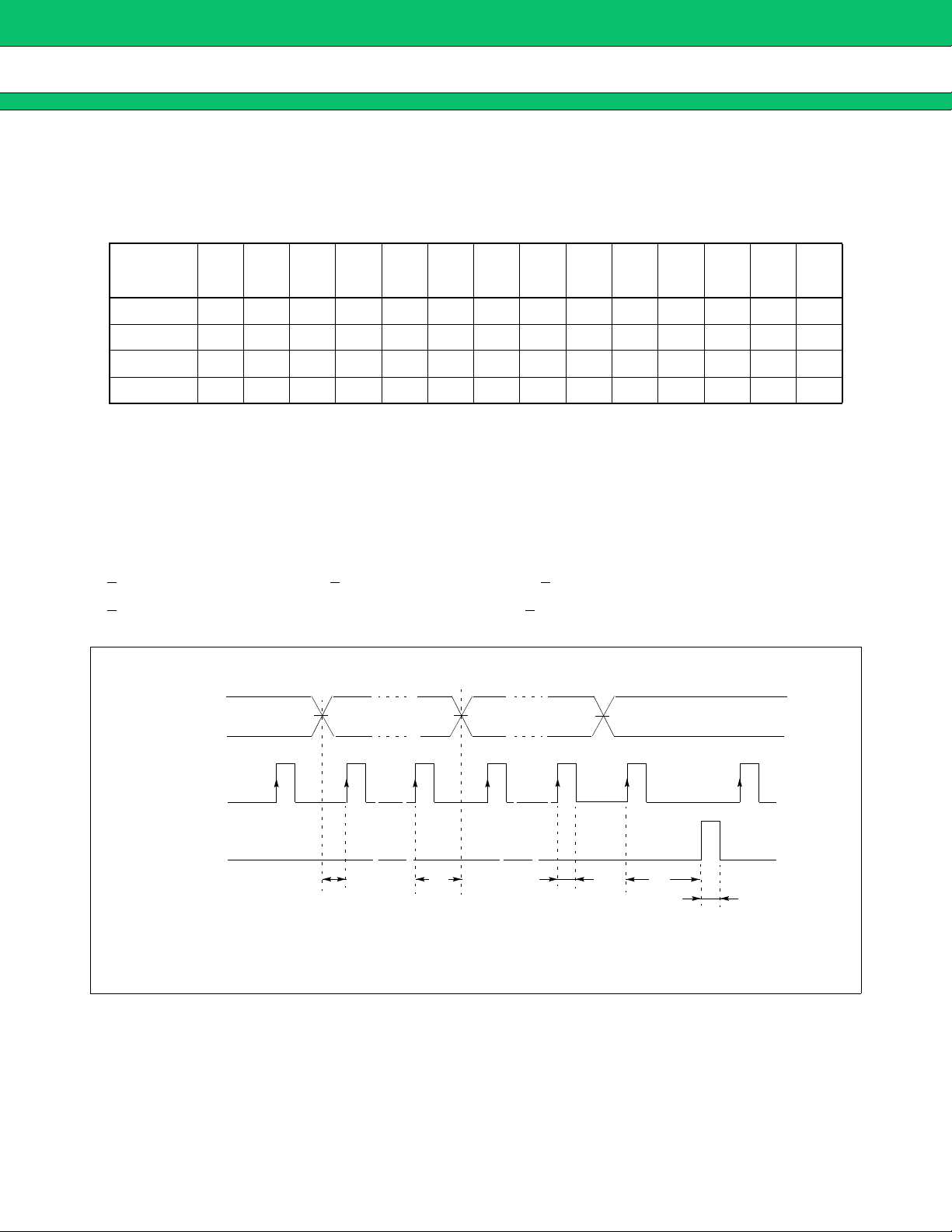
(5) Setting data input timing
The MB15C02 uses 19 bits of serial data f or the pro gramm able d ivider and 15 bi ts f or the prog rammab le ref er ence
divider . When more bits of serial data than d efined for the target divider are received, only the last val id serial data
bits are effective.
To set the divide ratio for the MB15C02 dividers, it is necessary to supply the Data, Clock, and LE signals at the
timing shown in Figure 5.
t
1 (>1 µs): Data setup time t2 (>1 µs): Data hold time t3 (> µs): Clock pulse width
t
4 (>1 µs): LE setup time to the rising edge of last clock t5 (>1 µs): LE pulse width
Data
Clock
LE
t1
t2
t3
Figure 5. Serial data input timing
t4
t5
14
Page 15

MB15C02
Since the divide rations are unpredictable when the MB15C02 is turned on, it is necessar y to initialize the divide
ratio for both dividers at power-on time. As shown in Figure 6, after setting the divide ratio for one of the dividers
(e.g., progra mmab le ref er ence divider), set LE to “H” le v el bef o re setting the divide r atio f or the ot her dividers (e.g. ,
programmable divider) . To change the divide ratio of one of the divide r after initia lizatio n, input th e serial data only
for that divider (the divide ratio for the other divider is preserved).
Data
Clock
LE
Serial data for progra mmable reference divider
15 clocks 19 clocks
1*
Serial data for programmable divider
* : Control bit
Figure 6. Inputting serial data(Setting divisors)
0*
15
Page 16

MB15C02
■ TYPICAL CHARACTERISTICS
1. fin Input Sensitivity
20.0
10.0
0.0
−10.0
−20.0
−30.0
Input sensitivity (dBm)
−40.0
−50.0
fin input frequency vs. Input sensitivity
Ta = +25°C
V DD = 1.0 V
V
DD = 1.2 V
V
DD = 1.3 V
DD = 1.5 V
V
2. OSC
−60.0
0 100 200 300 400 500 600 700 800 900 1000
IN Input Sensitivity
20.0
10.0
0.0
−10.0
−20.0
−30.0
Input sensitivity (dBm)
−40.0
−50.0
fin input frequency (MHz)
OSC
IN input frequency vs. Input sensitivity
Ta = +25°C
V DD = 1.0 V
V
DD = 1.2 V
V
DD = 1.3 V
V
DD = 1.5 V
16
−60.0
0 50 100 150 200 250 300 350 400 450 500
OSC
IN input frequency (MHz)
Page 17

3. fin Power Supply Voltage
MB15C02
(MHz)
1000
900
800
700
600
500
Input frequency (MHz)
400
300
200
100
0
Vfin = −2.0 (dBm)
0.9 1.0 1.1 1.2 1.3 1.4 1.6 1.7 1.8
Power supply voltage vs. fin input frequency
Ta = +25°C
1.5
Power supply voltage (V)
4. OSC
IN Power Supply Voltage
500
450
400
350
300
250
200
Input frequency (MHz)
150
100
50
0
Vfin = −2.0 (dBm)
0.9 1.0 1.1 1.2 1.3 1.4 1.6 1.7 1.8
Power supply voltage vs. OSC
Power supply voltage (V)
IN input frequency
Ta = +25°C
1.5
17
Page 18

MB15C02
5. IDD Power Supply Current
5.0
4.5
4.0
3.5
3.0
2.5
I DD (mA)
2.0
1.5
1.0
0.5
0.0
0 100 200 300 400 500 600 700 800 900 1000
Input frequency vs. power supply current
Input frequency (MHz)
Ta = +25°C
V DD = 1.0 V
V
DD = 1.2 V
V
DD = 1.3 V
V
DD = 1.5 V
18
Page 19

6. Do (Charge Pump) Power Supply Voltage
5.0
4.5
4.0
3.5
3.0
I OL (mA)
2.5
2.0
1.5
1.0
V
DD (V p) vs. I OL
(at V OL = 0.2 V)
MB15C02
Ta = +25°C
0.5
0.0
0.8 0.9 1.0 1.1 1.2 1.3 1.5 1.6 1.7 1.8
V
DD (V)
V
DD (V p) vs. I OH
(at V OH = V DD – 0.2 V)
–5.0
–4.5
–4.0
–3.5
–3.0
–2.5
I OH (mA)
–2.0
–1.5
–1.0
1.4
Ta = +25°C
–0.5
0.0
0.8 0.9 1.0 1.1 1.2 1.3 1.5 1.6 1.7 1.8
V
DD (V)
1.4
19
Page 20

MB15C02
7. Spectrum Wave Form
ATTEN 10 dB
RL 0 dBm
∆MKR
25.0 kHz
D
−85.50 dB
S
CENTER 286.0000 MHz
*RBW 1.0 kHz VBW 1.0 kHz
ATTEN 10 dB
RL 0 dBm
∆MKR
800 Hz
D
−53.84 dB
S
UAUG 16
10dB/
UAUG 50
10dB/
∆MKR −85.50 dB
25.0 kHz
SPAN 200.0 kHz
*SWP 1.00 s
∆MKR −53.84 dB
800 Hz
• LOCK Frequency : 286.0 MHz
(fr = 25 kHz)
DD = 1.2 V, V p = 1.2 V
• V
Ta = +25°C
• LOCK Frequency : 286.0 MHz
( fr = 25 kHz)
DD = 1.2 V, V p = 1.2 V
• V
Ta = +25°C
20
• Test circuit
D O VT (to VCO)
CENTER 286.00000 MHz
*RBW 100 Hz VBW 100 kHz
4.3 kΩ
6800 pF
68000 pF
SPAN 20.00 kHz
*SWP 3.00 s
15 kΩ
4700 pF
* VCO : K
V = 6 MHz/v
Page 21

8. Lock Up Time
• LOCK Frequency: 290.0 MHz to 286.0 MHz
(fr = 25 kHz)
•V
DD = 1.2 V, VP = 1.2 V, Ta = +25°C
290.0 MHz → 286.0 MHz, within ± 1 kHz
x : 3.99999984 ms
∆MKr A euts N/A
y : −4.00100 MHz
286.0050
MHz
2.00
kHz/div
MB15C02
4.00 ms
285.9950
MHz
0 s 10.0000000 ms
• LOCK Frequency: 286.0 MHz to 290.0 MHz
(fr = 25 kHz)
•V
DD = 1.2 V, VP = 1.2 V, Ta = +25°C
286.0 MHz → 290.0 MHz, within ± 1 kHz
x : 6.19999943 ms
∆MKr A euts N/A
y : 4.00082 MHz
290.0050
MHz
2.00
kHz/div
289.9950
MHz
6.20 ms
0 s 10.0000000 ms
(Continued)
21
Page 22

MB15C02
(Continued)
• LOCK Frequency: PS on to 286.0 MHz
(fr = 25 kHz)
•V
DD = 1.2 V, VP = 1.2 V, Ta = +25°C
PS ON → 286.0 MHz, within ± 1 kHz
∆MKr A euts N/A
286.0050
MHz
2.00
kHz/div
2.00 ms
x : 1.99999978 ms
y : −680 Hz
285.9950
MHz
0 s 8.0000000 ms
PS
1 V
0 V
■ USA GE PRECAU TIONS
• This device should be transported and stored in anti-static containers.
• This is a static-sensitive device; take proper anti- ESD precautio ns. Ensure that personnel and equipm ent are
properly grounded. Cover workbenches with grounded conductive mats.
• Always turn the power supply off before inserting or removing the device from its socket.
• Protect leads with a conductive sheet when handling or transporting PC boards with devices.
■ ORDERING INFORMATION
Parts number Package Remarks
MB15C02PFV1
MB15C02PFV2
16-pin Plastic SSOP
(FPT-16P-M05)
20-pin Plastic SSOP
(FPT-20P-M03)
22
Page 23

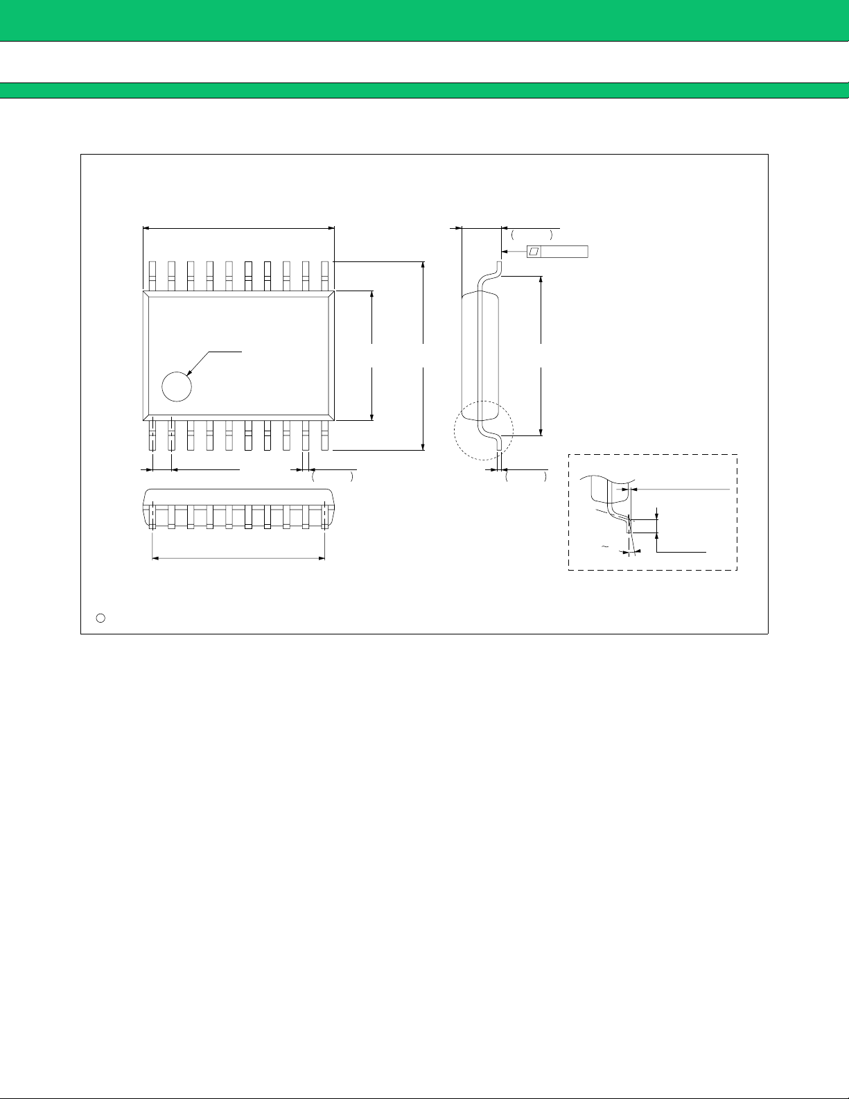
■ PACKAGE DIMENSIONS
MB15C02
16 pins, Plastic SSOP
(FPT-16P-M05)
*
5.00±0.10(.197±.004)
INDEX
0.65±0.12
(.0256±.0047)
4.55(.179)REF
*
4.40±0.10 5.40(.213)
(.173±.004) (.252±.008) NOM
+0.10
–0.05
0.22
+.004
–.002
.009
6.40±0.20
"A"
*: These dimensions do not include resin protrusion.
+0.20
1.25
–0.10
(Mounting height)
+.008
–.004
.049
0.10(.004)
0.15
.006
+0.05
–0.02
+.002
–.001
Details of "A" part
0 10°
0.10±0.10(.004±.004)
(STAND OFF)
0.50±0.20
(.020±.008)
C
1994 FUJITSU LIMITED F16013S-2C-4
Dimensions in mm (inches)
(Continued)
23
Page 24
MB15C02
(Continued)
20 pins, Plastic SSOP
(FPT-20P-M03)
*
6.50±0.10(.256±.004)
INDEX
0.65±0.12
(.0256±.0047)
5.85(.230)REF
*: These dimensions do not include resin protrusion.
*
4.40±0.10 5.40(.213)
(.173±.004) (.252±.008) NOM
+0.10
0.22
–0.05
+.004
.009
–.002
6.40±0.20
"A"
1.25
.049
0.15
.006
+0.20
–0.10
+.008
–.004
0.10(.004)
+0.05
–0.02
+.002
–.001
(Mounting height)
Details of "A" part
0 10°
0.10±0.10(.004±.004)
(STAND OFF)
0.50±0.20
(.020±.008)
C
1994 FUJITSU LIMITED F20012S-2C-4
Dimensions in mm (inches)
24
Page 25

MEMO
MB15C02
25
Page 26

MB15C02
MEMO
26
Page 27

MEMO
MB15C02
27
Page 28

FUJITSU MICROELECTRONICS LIMITED
Shinjuku Dai-Ichi Seimei Bldg. 7-1, Nishishinjuku 2-chome, Shinjuku-ku,
Tokyo 163-0722, Japan Tel: +81-3-5322-3347 Fax: +81-3-5322-3387
http://jp.fujitsu.com/fml/en/
For further information please contact:
North and South America
FUJITSU MICROELECTRONICS AMERICA, INC.
1250 E. Arques Avenue, M/S 333
Sunnyvale, CA 94085-5401, U.S.A.
Tel: +1-408-737-5600 Fax: +1-408-737-5999
http://www.fma.fujitsu.com/
Europe
FUJITSU MICROELECTRONICS EUROPE GmbH
Pittlerstrasse 47, 63225 Langen,
Germany
Tel: +49-6103-690-0 Fax: +49-6103-690-122
http://emea.fujitsu.com/microelectronics/
Korea
FUJITSU MICROELECTRONICS KOREA LTD.
206 KOSMO TOWER, 1002 Daechi-Dong,
Kangnam-Gu,Seoul 135-280
Korea
Tel: +82-2-3484-7100 Fax: +82-2-3484-7111
http://www.fmk.fujitsu.com/
Asia Pacific
FUJITSU MICROELECTRONICS ASIA PTE LTD.
151 Lorong Chuan, #05-08 New Tech Park,
Singapore 556741
Tel: +65-6281-0770 Fax: +65-6281-0220
http://www.fujitsu.com/sg/services/micro/semiconductor/
FUJITSU MICROELECTRONICS SHANGHAI CO., LTD.
Rm.3102, Bund Center, No.222 Yan An Road(E),
Shanghai 200002, China
Tel: +86-21-6335-1560 Fax: +86-21-6335-1605
http://cn.fujitsu.com/fmc/
FUJITSU MICROELECTRONICS PACIFIC ASIA LTD.
10/F., World Commerce Centre, 11 Canton Road
Tsimshatsui, Kowloon
Hong Kong
Tel: +852-2377-0226 Fax: +852-2376-3269
http://cn.fujitsu.com/fmc/tw
All Rights Reserved.
The contents of this document are subject to change without notice.
Customers are advised to consult with sales representatives before ordering.
The information, such as descriptions of function and application circuit examples, in this document are presented solely for the purpose
of reference to show examples of operations and uses of FUJITSU MICROELECTRONICS device; FUJITSU MICROELECTRONICS
does not warrant proper operation of the device with respect to use based on such information. When you develop equipment incorporating the device based on such information, you must assume any responsibility arising out of such use of the information.
FUJITSU MICROELECTRONICS assumes no liability for any damages whatsoever arising out of the use of the information.
Any information in this document, including descriptions of function and schematic diagrams, shall not be construed as license of the use
or exercise of any intellectual property right, such as patent right or copyright, or any other right of FUJITSU MICROELECTRONICS
or any third party or does FUJITSU MICROELECTRONICS warrant non-infringement of any third-party's intellectual property right or
other right by using such information. FUJITSU MICROELECTRONICS assumes no liability for any infringement of the intellectual
property rights or other rights of third parties which would result from the use of information contained herein.
The products described in this document are designed, developed and manufactured as contemplated for general use, including without
limitation, ordinary industrial use, general office use, personal use, and household use, but are not designed, developed and manufactured
as contemplated (1) for use accompanying fatal risks or dangers that, unless extremely high safety is secured, could have a serious effect
to the public, and could lead directly to death, personal injury, severe physical damage or other loss (i.e., nuclear reaction control in
nuclear facility, aircraft flight control, air traffic control, mass transport control, medical life support system, missile launch control in
weapon system), or (2) for use requiring extremely high reliability (i.e., submersible repeater and artificial satellite).
Please note that FUJITSU MICROELECTRONICS will not be liable against you and/or any third party for any claims or damages arising
in connection with above-mentioned uses of the products.
Any semiconductor devices have an inherent chance of failure. You must protect against injury, damage or loss from such failures by
incorporating safety design measures into your facility and equipment such as redundancy, fire protection, and prevention of over-current
levels and other abnormal operating conditions.
Exportation/release of any products described in this document may require necessary procedures in accordance with the regulations of
the Foreign Exchange and Foreign Trade Control Law of Japan and/or US export control laws.
The company names and brand names herein are the trademarks or registered trademarks of their respective owners.
Edited Strategic Business Development Dept.
 Loading...