

Page 1
Fujitsu Microelectronics Europe
User Guide
F²MC-16LX FAMILY
FMEMCU-UG-900001-32
EVALUATION BOARD
FLASH-CAN-100
USER GUIDE
Page 2

Change even page title here
Revision History
Revision History
Date Version Issue
07.12.98 V1.0 P14,P16 connected to JP7, JP8 (RS232 interface for MB90F594A)
must be changed
07.12.98 V1.0 Jumper on JP10, JP9 Pin2+3 must be changed to Pin 1+2
to connect to UART1
07.12.98 V1.2 Silk-Plot: Version number must be added.
07.12.98 V1.2 Silk-Plot: SIT/SOT is not correct. Must be changed.
07.12.98 V1.2 Silk-Plot: CAN100BOARD is not correct.
07.12.98 V1.2 Silk-Plot: In RS232 Jumper area - naming of pins must be changed
from Pxx to Pinxx.
07.12.98 V1.2 Silk-Plot: In CAN Jumper area - naming of pins must be changed
from Pxx to Pinxx.
07.12.98 V1.2 JP13 was not placed on the board.
07.12.98 V1.2 Allow connection of X4 (RS232 Sub-D-9 female) Pin 7+8
on the DIP switch S3 Pin 5.
13.01.99 V1.1 Page 6 of this manual - item 6.4 not X3 – must be X4
01.02.99 V1.2 Fig. 2 – Schematic of Flash-CAN-100P-M06 misprint: External voltage
supply plug must have Gnd on the inside and +12V on the outside.
03.02.99 V1.2 Disclaimer added to manual
03.02.99 V1.2 Manual revised to include information about Flash programming
software tools, which in now available in this package
12.02.99 V1.2a MB90580 series added – Can be used with this board also (only QFP
100 package!)
17.05.99 V2.0 Silk Plot changed to new Name: FLASH-CAN2-100P-M06
17.05.99 V2.0 New Socket Adapter for MCU used (NQPACK100RB)
17.05.99 V2.0 FLASH-CAN2-100P-M06 added in documentation
17.05.99 V2.0 Revised Silk plot in documentation
26.05.99 V2.0 Replace Pxx by Pixx in Chapter 5
26.05.99 V2.0 Chapter 6 – DIP-switch setting revised for asynchronous loader
software
26.05.99 V2.0 Table1 + 2 added in this document
16.07.99 X0+X1 are not available on socket pin
16.07.99 V2.0: Connection of new socket adapter must be watched carefully.
MCU might not have good contact
21.07.99 V2.1 Schematic of board added to this manual
05.08.99 V2.1 Attached Floppy modified to incl. Softune Worbench Projects
see \readme.txt – Revision V1.2
UG-900001-32 - 2 - © Fujitsu Microelectronics Europe GmbH
Page 3
Change odd page title here
Revision History
Date Version Issue
23.08.99 V2.2 Table 2. MB90F543 UART0 is wrong – it must be UART1
17.04.00 V2.3 Table 2 corrected now
17.04.00 V2.3 Chapter 1.1. Regarding connectivity problems added.
FLASH-CAN-100P-M06 is available again
09.01.01 V2.4 Support added for MB90F42x series
25.01.01 V2.5 Support for MB90F546G/GS and MB90F548G/GS series added,
Description of Connector JP11 added
19.09.01 V2.6 Support for MB90440G series added, new disclaimer added
05.10.01 V2.7 New disclaimer corrected
13.02.02 V2.8 chapter 5.1 (MB90470) added Hardware: U6 changed to
MAX3232CPE
22.08.02 V2.9 new style; MB90435, MB90480 added
07/02/03 V3.0 Disclaimer corrected
V3.1 Series support, device list corrected
27.11.06 V3.2 Changed Socket Information
This document contains 20 pages.
© Fujitsu Microelectronics Europe GmbH - 3 - UG-900001-32
Page 4

Change even page title here
Warranty and Disclaimer
Warranty and Disclaimer
To the maximum extent permitted by applicable law, Fujitsu Microelectronics Europe GmbH restricts
its warranties and its liability for the FLASH-CAN-100P-M06 Board and all its deliverables (eg.
software include or header files, application examples, target boards, evaluation boards, engineering
samples of IC’s etc.), its performance and any consequential damages, on the use of the Product in
accordance with (i) the terms of the License Agreement and the Sale and Purchase Agreement under
which agreements the Product has been delivered, (ii) the technical descriptions and (iii) all
accompanying written materials. In addition, to the maximum extent permitted by applicable law,
ujitsu Microelectronics Europe GmbH disclaims all warranties and liabilities for the performance of
F
the Product and any consequential damages in cases of unauthorised decompiling and/or reverse
engineering and/or disassembling. Note, the FLASH-CAN-100P-M06 Board and all its deliverables
are intended and must only be used in an evaluation laboratory environment.
1. Fujitsu Microelectronics Europe GmbH warrants that the Product will perform substantially in
accordance with the accompanying written materials for a period of 90 days form the date of
receipt by the customer. Concerning the hardware components of the Product, Fujitsu
Microelectronics Europe GmbH warrants that the Product will be free from defects in material
and workmanship under use and service as specified in the accompanying written materials
for a duration of 1 year from the date of receipt by the customer.
2. Should a Product turn out to be defect, Fujitsu Microelectronics Europe GmbH´s entire liability
and the customer´s exclusive remedy shall be, at Fujitsu Microelectronics Europe GmbH´s
sole discretion, either return of the purchase price and the license fee, or replacement of the
Product or parts thereof, if the Product is returned to Fujitsu Microelectronics Europe GmbH in
original packing and without further defects resulting from the customer´s use or the transport.
However, this warranty is excluded if the defect has resulted from an accident not attributable
to Fujitsu Microelectronics Europe GmbH, or abuse or misapplication attributable to the
customer or any other third party not relating to Fujitsu Microelectronics Europe GmbH.
3. To the maximum extent permitted by applicable law Fujitsu Microelectronics Europe GmbH
disclaims all other warranties, whether expressed or implied, in particular, but not limited to,
warranties of merchantability and fitness for a particular purpose for which the Product is not
designated.
4. To the maximum extent permitted by applicable law, Fujitsu Microelectronics Europe GmbH´s
and its suppliers´ liability is restricted to intention and gross negligence.
NO LIABILITY FOR CONSEQUENTIAL DAMAGES
To the maximum extent permitted by applicable law, in no event shall Fujitsu
Microelectronics Europe GmbH and its suppliers be liable for any damages whatsoever
(including but without limitation, consequential and/or indirect damages for personal
injury, assets of substantial value, loss of profits, interruption of business operation,
loss of information, or any other monetary or pecuniary loss) arising from the use of
the Product.
Should one of the above stipulations be or become invalid and/or unenforceable, the remaining
stipulations shall stay in full effect
UG-900001-32 - 4 - © Fujitsu Microelectronics Europe GmbH
Page 5

Change odd page title here
Contents
Contents
REVISION HISTORY............................................................................................................ 2
WARRANTY AND DISCLAIMER ......................................................................................... 4
CONTENTS .......................................................................................................................... 5
1 OVERVIEW...................................................................................................................... 6
1.1 Abstract................................................................................................................... 6
1.2 Introduction ............................................................................................................. 6
1.3 Connectivity problems of the socket adapter ........................................................... 6
2 FEATURES...................................................................................................................... 7
3 SUPPORTED MICROCONTROLLER SERIES................................................................ 8
4 DELIVERABLES.............................................................................................................. 9
5 CONFIGURATION OF THE EVALUATION-BOARD ..................................................... 10
5.1 Modifications for use with MB90470 / MB90480 series.......................................... 12
5.1.1 Schematic of the modifications for MB90470 / MB90480 ......................... 13
6 USING THE ASYNCHRONOUS BOOT-LOADER ......................................................... 14
7 CONNECTORS.............................................................................................................. 15
7.1 Power connector (X1)............................................................................................ 15
7.2 Edge connector (J2, J3, J4, J5)............................................................................. 15
7.3 GND/VCC (JP11) .................................................................................................. 15
7.4 UART (X4)............................................................................................................. 16
7.5 CAN Interface (X2, X3).......................................................................................... 16
8 SILK-PLOT OF THE BOARD ........................................................................................ 17
9 SCHEMATIC OF THE BOARD ...................................................................................... 18
10 RELATED PRODUCTS ................................................................................................. 19
11 INFORMATION IN THE WWW....................................................................................... 20
© Fujitsu Microelectronics Europe GmbH - 5 - UG-900001-32
Page 6

Change even page title here
Chapter 1 Overview
1 Overview
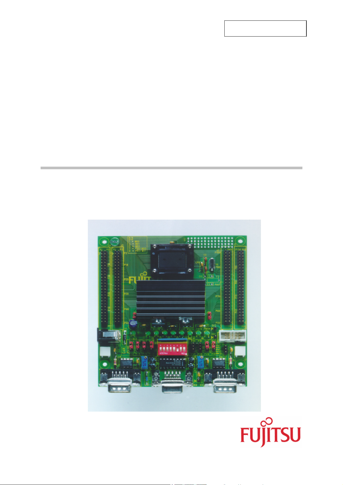
1.1 Abstract
This user guide describes the basic features of the new FLASH-CAN-100P-M06/FLASHCAN2-100P-M06 board. This board can be used with almost all our 16LX microcontroller
series supporting the FPT-100P-M06 package.
1.2 Introduction
The "Flash/CAN100"-board was developed in order to support customers and allow a fast
software design start. Fujitsu emulators require a target system that provides Vcc and GND
as well as an oscillation circuit. Additionally most of Fujitsu’s flash microcontroller support the
burn-in flash programming algorithm.
For the FLASH-CAN-100P-M06 board an IC149-100-114-B5 socket adapter is used. The
suitable emulation probe cable is the MB2132-457.
On the FLASH-CAN2-100P-M06 board a NQPACK100RB socket adapter is assembled.
This requires the MB2132-464 for the connection to the emulator.
This board must only be used for test applications
in an evaluation laboratory environment.
1.3 Connectivity problems of the socket adapter
Some customers experience connectivity problems when connecting the MCU into the
socket adapter. Only the small red screwdriver available in your box should be used to
connect the cover (HQPACK) onto the socket (NQPACK).
If the four screws are not tightening equally, then it may cause a poor contact.
Do not screw the cover too tight (max 0.054 Nm). If you have connectivity problems then
please loosen the screws and tighten again the screws equally.
Do not clean NQPACK, YQPACK, and YQSOCKET with steam. Cleaning material will
contaminate inside of connector.
Customers using the FLASH-CAN-100P-M06 (with IC-149-100-114-B5 socket adapter) do
usually not encounter this problem with the FLASH device.
UG-900001-32 - 6 - © Fujitsu Microelectronics Europe GmbH
Page 7

Change odd page title here
Chapter 2 Features
2 Features
< a new 100-pin socket adapter for better connectivity
< 7-14V unstabilized external DC power supply possible
< 5V and 3.7V internal power supply available
< two high-speed CAN drivers
< one RS232 interface
< two identical pin connectors for all MCU pins
< optional sub-clock
< RST, HST push-button
< 8 User-LEDs
< external reset via RS232
< Flash-Programming Software for PC’s
The target board will be delivered with the MB90F598G single-CAN, 128KByte flash
microcontroller. This microcontroller contains the 'burn-in'-boot loader for programming the
flash.
© Fujitsu Microelectronics Europe GmbH - 7 - UG-900001-32
Page 8

Change even page title here
Chapter 3 Supported Microcontroller Series
3 Supported Microcontroller Series
The target board was designed to work with many microcontrollers from the F²MC-16LX
family. As it allows the programming of blank flash devices and supports high speed CAN
interfaces, this board is ideal as a test at design start. The following microcontroller series
can be used with this board:
< MB90420G = MB90V420G, MB90F428GA/GB/GC etc.
< MB90435 = MB90V540, MB90F437, MB90F438, MB90F439 etc.
< MB90440G = MB90V440G, MB90F443G etc.
< MB90470* = MB90V470B, MB90F474L, MB90F474H etc.
< MB90480* = MB90V480, MB90F481, MB90F482, MB90F483, etc.
< MB90540G = MB90V540G, MB90F543G/GS, MB90F546G/GS etc.
< MB90550 = MB90V550, MB90F553A, MB90553A, etc.
< MB90580 = MB90V580, MB90F583, MB90583, etc.
< MB90590G = MB90V590G, MB90F594/A/G, MB90594/A/G, MB90591/G, etc.
< MB90595G = MB90V595, MB90F598, MB90598, etc.
* modifications are necessary for FlashCAN100P-M06: see chapter 5.1
UG-900001-32 - 8 - © Fujitsu Microelectronics Europe GmbH
Page 9

Change odd page title here
Chapter 4 Deliverables
4 Deliverables
"FLASH-CAN-100P-M06"/"FLASH-CAN2-100P-M06" will be delivered with:
< the Flash/CAN100 board itself
< two 50pin socket connectors
< power supply connector
< MB90F598 - 128KB flash microcontroller
< 11 Jumper
< 1 socket adapter cover
< documentation
< Flash programming utility – floppy disc
For software add-ons please contact your local technical support team for the latest software
release or Flash-Programming tools.
© Fujitsu Microelectronics Europe GmbH - 9 - UG-900001-32
Page 10

Change even page title here
Chapter 5 Configuration of the Evaluation-Board
5 Configuration of the Evaluation-Board
The board is configured to work with the MB90F598 microcontroller.
In order to set up the board follow these steps:
1. disconnect power supply disconnected !
2. Set jumper JP1 to provide Vcc, i.e. 5V to the board
3. If case one is connecting this board to an emulator, it is recommended to set jumper JP2
in order to provide 3.7V to the internal core.
4. Please set the mode pins 1-3 on S3 according to your MCU operating mode. ON stands
for 0 and OFF for 1. E.g. MB90F598 all switches to OFF except no. 3.
5. Adjust both potentiometers (P1, P2) clockwise to their end position.
(Check that Pin 8 of U4 and Pin 8 of U5 are grounded.)
6. Select the appropriate CAN interface for the microcontroller you are using by setting
jumper JP3-JP6. Note that Pixx on the silk plot stands for Pinxx, i.e. the pin number.
E.g. for the MB90F598, set JP3 and JP4 to connect Pin 2 and 3 in order to connect to
MCU Pins 74 and 75, respectively.
Target
Series
CAN0 CAN1 CAN2
RX0 TX0 RX1 TX1 RX2 TX2
MB90425 Pin 75 Pin 74 n.a. n.a. n.a. n.a.
Pin 72 Pin 71
MB90440 Pin 74 Pin 73 Pin 76 Pin 75
(Not supported by
Jumper 3-6 !)
MB90470 n.a. n.a. n.a. n.a. n.a. n.a.
MB90540 Pin 74 Pin 73 Pin 76 Pin 75 n.a. n.a.
MB90545 Pin 74 Pin 73 n.a. n.a. n.a. n.a.
MB90550 n.a. n.a. n.a. n.a. n.a. n.a.
MB90583 n.a. n.a. n.a. n.a. n.a. n.a.
MB90590 Pin 75 Pin 74 Pin 97 Pin 98 n.a. n.a.
MB90595 Pin 75 Pin 74 n.a. n.a. n.a. n.a.
Table 1: Microcontroller pin-number of the CAN-interface
UG-900001-32 - 10 - © Fujitsu Microelectronics Europe GmbH
Page 11

Change odd page title here
Chapter 5 Configuration of the Evaluation-Board
7. Select the appropriate UART interface for the microcontroller you are using by setting
jumper JP7-JP10.
8. Please use 1:1 cable for PC-connection.
Notes:
< Pixx on the silk plot stands for Pinxx, i.e. the pin number.
e.g. for the MB90F598, set JP10 and JP9 to connect Pin 1 and 2 in order use UART 1
< MB90425, MB90470, MB90480 and MB90580 series are not supported by jumpers.
Please make handwired connections for these controllers.
Target Series
Asynch.
Com.
SIN / Jumper SOT / Jumper
handwire Pin 88 – JP10.2 handwire Pin 89 – JP9.2
MB90425 UART1
(Not supported by Jumper JP7 - JP10)
MB90435 UART1 Pin 21 (JP10:1-2) Pin 24 (JP9:1-2)
MB90440 UART1 Pin 21 (JP10:1-2) Pin 24 (JP9:1-2)
handwire Pin 27 – JP10.2 handwire Pin 28 – JP9.2
MB90470 UART0
(Not supported by Jumper JP7 - JP10)
see chapter 6.1 !
handwire Pin 27 – JP10.2 handwire Pin 28 – JP9.2
MB90480 UART0
(Not supported by Jumper JP7 - JP10)
see chapter 6.1 !
MB90540 UART1 Pin 21 (JP10:1-2) Pin 24 (JP9:1-2)
MB90545 UART1 Pin 21 (JP10:1-2) Pin 24 (JP9:1-2)
MB90550 UART0 Pin 20 (JP8:1-2) Pin 19 (JP7:1-2)
handwire Pin 18 – JP10.2 handwire Pin 19 – JP9.2
MB90580 UART0
(Not supported by Jumper JP7 - JP10)
MB90590 UART0 Pin 16 (JP8:2-3) Pin 14 (JP7:2-3)
MB90595 UART1 Pin 21 (JP10:1-2) Pin 24 (JP9:1-2)
Table 2: MCU pin-number used, for the asynchronous boot-loader software
© Fujitsu Microelectronics Europe GmbH - 11 - UG-900001-32
Page 12
Change even page title here
Chapter 5 Configuration of the Evaluation-Board
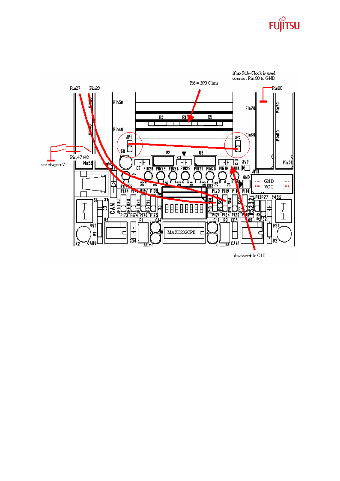
5.1 Modifications for use with MB90470 / MB90480 series
Some modifications have to be done in order to use the FLASH-CAN-100P Board together
with a MCU of the MB90470 / MB90480 series:
1. Check that U6 is MAX3232CPE
2. Change R6 470 => 390 Ohm. Check that output voltage of U3 is 3.3V (JP2)
3. Disassemble C10 (100nF)
4. Connect J4- Pin 27 to JP10- Pin 2 (SIN)
5. Connect J4- Pin 28 to JP9- Pin 2 (SOT)
6. Connect J5- Pin 80 to GND (X0A) if no Sub-Clock is used
Otherwise Sub-Clock crystal Y2 and capacitors C5, C6 has to be assembled
7. Remove JP1. Connect JP1- Pin 2 to JP2- Pin 1
8. Emulator-Settings:
1 2 3 4 5 6 7 8
SW1
check emulator-manual for clock-selection-switch
ON
OFF
S1
S2
A B C
A B C
Only MB90470series:
The MB90470 series normally uses 3V power-supply. However, some Ports (P2, P3, P4 and
P7) can operate with 5V. In this case Pin 23 (Vcc5) of the microcontroller has to be
disconnected from Vcc on the FLASH-CAN-100P Board but has to be connected to +5V.
Cutting a trace near the capacitor CB2 on the bottom layer of the board only can do this.
Caution with the probe-cable:
The probe-cable MB2132-457 (Yamaichi socket) can NOT be used for dual voltage
(Vcc3=+3V, Vcc5=+5V), because Pin 23 and Pin 84 (Vcc3 / Vcc5) are shortcut within the
probe-cable.
UG-900001-32 - 12 - © Fujitsu Microelectronics Europe GmbH
Page 13
Change odd page title here
Chapter 5 Configuration of the Evaluation-Board
5.1.1 Schematic of the modifications for MB90470 / MB90480
© Fujitsu Microelectronics Europe GmbH - 13 - UG-900001-32
Page 14

Change even page title here
Chapter 6 Using the Asynchronous Boot-Loader
6 Using the Asynchronous Boot-Loader
The asynchronous boot-loader SW from Fujitsu can be used to program a blank flash
microcontroller. This tool is available on the floppy disc. The following additional steps to
chapter 5 need to be taken to set up the hardware (power supply disconnected!):
1. Place the flash microcontroller in its socket (observe pin no. 1 position).
2. Set DIP switch (SW3) :
8 7 6 5 4 3 2 1
1,5,7,8 ON
2,3,4,6 OFF
MB90470 / MB90480 series only:
8 7 6 5 4 3 2 1
1,5 ON
2,3,4,6,7,8 OFF
additionally Pin 47 and 48 (Port P80,P81) have to be connected to GND
for MB90470 and MB90480 series only (see chapter 5.1)
3. Switch on the power supply.
4. Start the asynchronous boot loader software and follow the instructions.
5. Set DIP switch (SW3)
for RUN-Mode,
8 7 6 5 4 3 2 1
e.g. Single-Chip-Mode
3 ON
1,2,4,5,6,7,8 OFF
MB90470 / MB90480 series only:
disconnect Pin 47 and 48 (Port P80,P81) from GND (see chapter 5.1)
OFF
ON
OFF
ON
OFF
ON
6. Reset Target
UG-900001-32 - 14 - © Fujitsu Microelectronics Europe GmbH
Page 15

Change odd page title here
Chapter 7 Connectors
7 Connectors
7.1 Power connector (X1)
The following figure shows the power connection jack X1. This connector is used to connect
an external unregulated DC power supply voltage (9V-12V DC) to the evaluation board.
Connector X1:
Shield is connected to positive voltage supply
Centre is connected to ground (GND)
It is recommended to use 9V to keep the power dissipation to a minimum. Otherwise, an
additional heat sink for the linear voltage regulator might be necessary.
7.2 Edge connector (J2, J3, J4, J5)
All pins of the microcontroller (QFP-100 package) are directly connected to J2, J3, J4 and
J5, all are 2 x 25 Pin headers, as follows:
Connector MCU Pins
J2, J4 (1 – 50) 1 – 50
J3, J5 (51 – 100) 51 – 100
The odd pin numbers are located on the one side and the even pin numbers are located on
the other side of the connector.
On the PCB, the corresponding pin numbers of the TC are written next to the connector pins.
7.3 GND/VCC (JP11)
Vcc 1
Additionally Vcc and GND Pins
are placed on the board (JP11).
Vcc 3
Vcc 5
Vcc 7
Vcc 9
Pinning of JP11
© Fujitsu Microelectronics Europe GmbH - 15 - UG-900001-32
2 GND
4 GND
6 GND
8 GND
10 GND
Page 16

7.4 UART (X4)
Change even page title here
Chapter 7 Connectors
One 9-pin D-Sub female connectors are used
for the serial interface (UART).
TXD is the transmit output, RXD is the receive input.
The DTR signal can be used to generate a reset.
Please use 1:1 cable for PC-connection.
Connector X4:
7.5 CAN Interface (X2, X3)
Two 9-pin D-Sub male connector
are used for the CAN interface.
Adjust both potentiometers (P1, P2) clockwise
to their end position.
(Check that Pin 8 of U4 and Pin 8 of U5 are grounded.)
GND DTR RxD TxD
5
9
CTS RTS DSR
GND CANL
5
9
1
6
1
6
Connector X2, X3:
CANH
UG-900001-32 - 16 - © Fujitsu Microelectronics Europe GmbH
Page 17

Chapter 8 Silk-Plot of the board
8 Silk-Plot of the board
Change odd page title here
Silk Plot of the new FLASH-CAN2-100P-M06
© Fujitsu Microelectronics Europe GmbH - 17 - UG-900001-32
Page 18

Change even page title here
Chapter 9 Schematic of the board
9 Schematic of the board
UG-900001-32 - 18 - © Fujitsu Microelectronics Europe GmbH
Page 19

Change odd page title here
Chapter 10 Related Products
10 Related Products
< FLASH-CAN-100P-M06 Evaluation-board according to this user guide
< MB2132-457 Probe cable for socket: Yamaichi IC149-100-x14-y5
Yamaichi: http://www.yamaichi.de
< FLASH-CAN2-100P-M06 New Evaluation board according to this user guide
< MB2132-464 Probe cable for socket: Tokyo Eletech:
NQPack100rb / HQPack100rb179
Tokyo Eletech: http://www.tetc.co.jp/nq/e_nq_draw.htm
< MB2141A/B Emulator debugger main unit
< MB2145-507 Emulation POD
< MB90Vxxx Evaluation chip (please refer to chapter 3)
< MB90Fxxx Flash-Microcontroller (please refer to chapter 3)
note: choose package FPT-100P-M06
© Fujitsu Microelectronics Europe GmbH - 19 - UG-900001-32
Page 20

Change even page title here
Chapter 11 Information in the WWW
11 Information in the WWW
Information about FUJITSU MICROELECTRONICS Products
can be found on the following Internet pages:
Microcontrollers (8-, 16- and 32bit), Graphics Controllers
Datasheets and Hardware Manuals, Support Tools (Hard- and Software)
http://www.fme.gsdc.de/gsdc.htm
Memory products: Flash, SDRAM and FRAM
http://www.fme.fujitsu.com/products/memory/index1.html
Linear Products: Power Management, A/D and D/A Converters
http://www.fme.fujitsu.com/products/linear/start.html
Media Products: SAW filters, acoustic resonators and VCOs
http://www.fme.fujitsu.com/products/media/index1.html
For more information about FUJITUS MICROELECTRONICS
http://www.fme.fujitsu.com/products/start.html
UG-900001-32 - 20 - © Fujitsu Microelectronics Europe GmbH
 Loading...