

FUJIFILM FinePix A600 SERVICE MANUAL

DIGITAL CAMERA
FinePix A600
SERVICE MANUAL
US/EU/EG/EE/AS/CH-Model
CAUTION
BECAUSE THIS PRODUCTIS RoHS LEAD-FREE COMPLIANT, USE THE DESIG-
NATED AFTER-SELES PARTS AND THE DESIGNATED LEAD-FREE SOLDER WHEN
PERFORMING REPAIRS. (Refer to page 3 to page 5)
WARNING
THE COMPONENTS IDENTIFIED WITH THE MARK “ ” ON THE SCHEMATIC
DIAGRAM AND IN THE PARTS LIST ARE CRITICAL FOR SAFETY.
PLEASE REPLACE ONLY WITH THE COMPONENTS SPECIFIED ON THE SCHEMATIC
DIAGRAM AND IN THE PARTS LIST.
IF YOU USE PARTS NOT SPECIFIED, IT MAY RESULT IN A FIRE AND AN
ELECTRICAL SHOCK.
FUJI PHOTO FILM CO., LTD.
Ref.No.:ZM00638-100
Printed in Japan 2006.05

FinePix A600 Service Manual
SAFETY CHECK-OUT
After correcting the original problem, perform the following
safety check before return the product to the customer.
1. Check the area of your repair for unsoldered or poorly
soldered connections. Check the entire board surface
for solder splasher and bridges.
2. Check the interboard wiring to ensure that no wires are
“pinched” or contact high-wattage resistors.
3. Look for unauthorized replacement parts, particularly
transistors, that were installed during a previous repair.
Point them out to the customer and recommend their
replacement.
4. Look for parts which, though functioning, show obvious
signs of deterioration. Point them out to the customer
and recommend their replacement.
5. Check the B + voltage to see it is at the values
specified.
6. Make leakage - current measurements to determine
that exposed parts are acceptably insulated from the
supply circuit before returning the product to the
customer.
7. CAUTION: FOR CONTINUED
PROTECTION AGAINST FIRE
HAZARD, REPLACE ONLY WITH
SAME TYPE 2.5 AMPERES 125V
FUSE.
2.5A 125V
2.5A 125V
8. WARNING:
RISK OF FIREREPLACE FUSE
AS MARKED
ATTENTION: AFIN D'ASSURER
UNE PROTECTION
PERMANENTE CONTRE LES
RISQUES D'INCENDIE,
REMPLACER UNIQUEMENT
PAR UN FUSIBLE DE MEME,
TYPE 2.5 AMPERES, 125 VOLTS.
TO REDUCE THE ELECTRIC
SHOCK, BE CAREFUL TO
TOUCH THE PARTS.
WARNING!
HIGH VOLTAGE
2

FinePix A600 Service Manual
RoHS lead-free compliance
Because this product is RoHS lead-free compliant, use the designated after-sales parts and the designated lead-free solder
when performing repairs.
<Background & Overview>
With the exception of parts and materials expressly excluded from the RoHS directive (*1), all the internal connections and
component parts and materials used in this product are lead-free compliant (*2) under the European RoHS directive.
*1: Excluded items (list of the main lead-related items)
• Lead included in glass used in fluorescent tubes, electronic components and cathode-ray tubes
• Lead in high-melting-point solder (i.e. tin-lead solder alloys that contain 85% lead or more)
• Lead in ceramic electronic parts (piezo-electronic devices)
• Mercury contained in fluorescent tubes is also excluded.
*2: Definition of lead-free
A lead content ratio of 0.1 wt% or less in the applicable locations (solder, terminals, electronic components, etc.)
<Reference>
RoHS: The name of a directive issued by the European Parliament aimed at restricting the use of
certain designated hazardous substances included in electrical and electronic equipment.
Designated substances (6): Lead, mercury, cadmium, hexavalent chromium, polybrominated biphenyls (PBBs) and
polybrominated diphenyl ether (PBDE)
<Lead-free soldering>
When carrying out repairs, use a designated lead-free solder, bearing in mind the differing work practices for conventional
solder (eutectic) and lead-free solder.
Differences in the soldering work for lead-free and eutectic solder
When the soldering work practices for eutectic solder and lead-free solder are compared, the main differences are as shown
below. In particular, when lead-free solder is used, the solder tends to be less workable than when eutectic solder is used.
Accordingly, the soldering techniques used must take that into account.
Difference
The solder starts melting later.
1
Poor wetting
2
Solder feed rate is difficult to control.
3
Wetting the insides of through holes is especially
4
difficult.
5
During repairs (or modifications) removing solder
from inside through holes is difficult.
6
There is serious carbonization of the soldering iron.
The surface is not glossy.
7
The initial melting point of lead-free solder is high, so you
have to get used to it.
Move the tip of the soldering iron around to heat the entire
connection to the melting temperature and assist wetting.
Use the solder (wire) diameter and soldering iron that are
best suited to connection being soldered.
First apply solder to the area immediately around the
through hold and then feed the solder into the hole.
Use a suitable wicking wire (with a suitable method and
heating) and a suction tool.
Either put solder onto the soldering iron tip after completing
the work, or turn the iron off frequently.
Learn to recognize the appearance of the surface.
Countermeasure
3
FinePix A600 Service Manual
Setting temperature during lead-free soldering
• Lead-free solder melting temperature
The melting point of eutectic (Sn-Pb) solder is 183°C, while the melting point of lead-free solder (Sn-Ag-Cu) is 30°C higher
at 220°C.
• Soldering iron tip temperature
The temperature setting for the soldering iron used should be such that the tip of the soldering iron is at the correct
bonding temperature for the connection. This temperature is normally set at around 100°C higher than the melting point of
the solder.
However, the actual temperature should take into account the shape and size of the soldering iron tip, the heat tolerance
of the connection and the workability of that temperature.
• Correct bonding temperature
The correct bonding temperature refers not to the temperature of the heat source, but to the bonding temperature that will
give the best bond strength.
Precautions when soldering with lead-free solder
• Soldering iron maintenance
Because of the high soldering iron temperature in lead-free soldering, there is rapid carbonization of the flux adhering to
the tip of the soldering iron.
(1) Always cover the tip of the soldering iron with solder when it is not being used.
(2) If the tip is black from carbonization, wipe it gently with a paper towel soaked in alcohol until the solder will wet.
• Uniform heating of the board and components
To ensure that the lead-free solder wets the entire surface of the pattern and the lands despite its poor wetting
characteristics, you must move the tip of the soldering iron over a wide area to raise the temperature of the entire
connection.
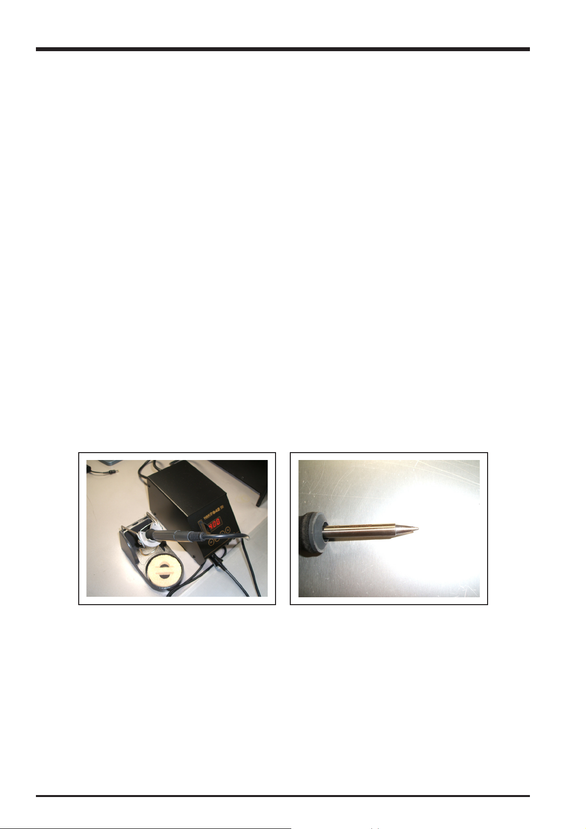
Soldering iron
A soldering iron with a temperature control is best.
4
FinePix A600 Service Manual
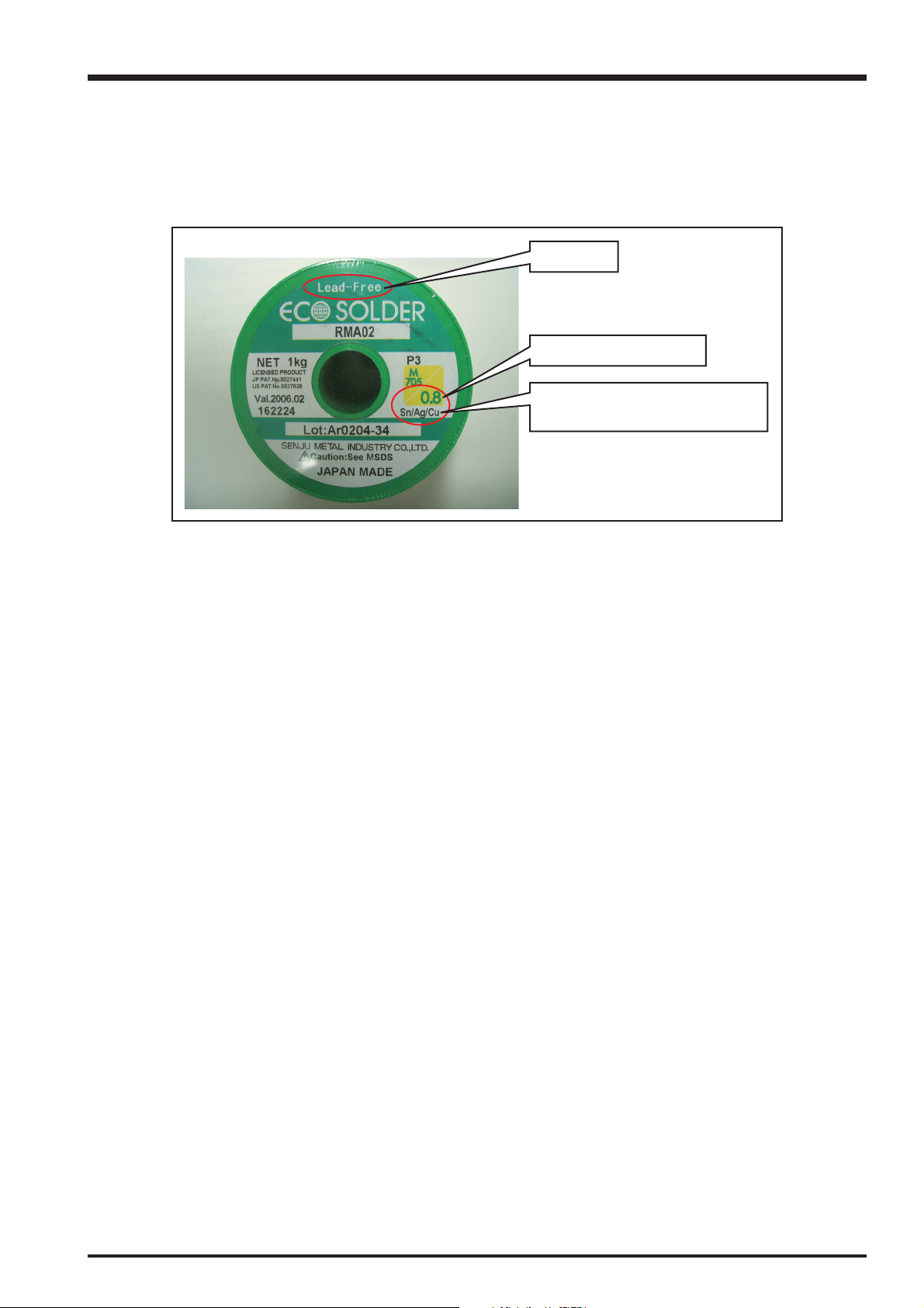
Solder wire (thread)
Use the lead-free solders specified below.
Solder type: Sn96.5Ag3Cu0.5 (Displayed symbol: SnAgCu)
Wire diameter: 0.6, 0.8 or 1.0 mm
Sample:
lead-free
Wire diameter 0.8mm
Solder type (Displayed symbol)
SnAgCu
Flux
Conventional flux can be used.
Solder application wires (mesh, wicking wire, etc.)
Conventional application wires can be used.
5

MEMO
FinePix A600 Service Manual
6

FinePix A600 Service Manual
CONTENTS
CONTENTS
1. General ........................................................... 8
1-1. Product specification .............................................. 8
1-2. Explanation of Terms ............................................ 11
1-3. Names of External Components .......................... 12
2. Disassembly ................................................. 13
2-1. Names of internal Components ............................13
2-2. Removing the REAR COVER .............................. 14
2-3. Removing the LCD COVER ................................. 15
2-4. Removing the SHUTTER BUTTON unit .............. 16
2-5. Removing the MAIN PWB ASSY .......................... 16
2-6. Removing the LENS UNIT ................................... 18
2-7. Removing the CCD .............................................. 18
2-8. Removing the BATTERY BOX ............................. 19
2-9. Removing the FLASH UNIT ................................. 21
2-10. TFT SHEET installation location .......................... 21
3. Schematics ................................................... 23
3-1. Cautions ............................................................... 23
3-2. Basic Block Names and Functions .......................23
3-3. Functions of Primary Blocks ................................. 24
3-3-1. Technical Outline .................................... 24
3-4. Block Diagram ...................................................... 25
3-5. Overall connection Diagram ................................. 26
3-6. Circuit Diagrams ...................................................27
3-6-1. CAMERA BLOCK ................................... 27
3-6-2. DCDC BLOCK ........................................ 28
3-6-3. MOTOR BLOCK ..................................... 29
3-6-4. PROCESS BLOCK .................................30
3-6-5. AUDIO BLOCK ....................................... 31
3-6-6. CCD FPC BLOCK ................................... 32
3-6-7. FLASH BLOCK .......................................33
3-6-8. SUB PWB BLOCK ..................................33
3-6-9. KEY BLOCK ........................................... 34
3-6-10. LCD BLOCK ........................................... 35
3-7. Mounted Parts Diagrams ...................................... 36
3-7-1. CCD FPC ASSY ..................................... 36
3-7-2. MAIN PWB ASSY ...................................39
3-7-3. SUB PWB ASSY ..................................... 40
4. Adjustments .................................................. 41
4-1. Important point before Adjustment ....................... 41
4-1-1. The handling of image files in internal
memory ................................................... 41
4-1-2. Adjustment when Replacing
Major Parts ............................................. 42
4-2. Measuring Instruments Used ............................... 42
4-3. Use Jig ................................................................. 43
4-3-1. Jig list ...................................................... 43
4-3-2.
4-4. Calibration method of pattern box ........................ 44
4-5. Adjustment software installation ........................... 45
4-5-1. Various downloading software
4-5-2. Installation of DSC jig driver ................... 46
4-5-3. Adjustment softwareinitiation method ..... 46
4-6. Initial Settings of the Adjustment Software ........... 47
4-7. Starting the Adjustment Software ......................... 50
4-8. [R] : Flash Memory Reset ..................................... 53
4-9. [F4] : CCD Defect Correction/OFD Adjustment ....55
4-10. [F5] : Camera Adjustment ..................................... 58
4-11. [F6] : AF Adjustment .............................................62
4-12. [F7] : Flash Adjustment ......................................... 65
4-13. [F1] : Battery Voltage Adjustment ......................... 67
4-14. [F11] : Video Adjustment ...................................... 71
4-15. [F3] : LCD Adjustment .......................................... 73
4-16. [F8] : Firmware Download .................................... 75
4-17. [F12] : End Setting................................................ 77
Modifying the FxA500/A400 Battery jig
decompressions, preservation methods,
and notes ................................................45
...... 43
5. Inspection ..................................................... 81
5-1. Required Measuring Equipment ...........................81
5-2. Connection of Measuring Equipment ................... 81
5-3. Inspection and Factory Settings ........................... 82
6. Parts List....................................................... 87
6-1. Packing and Accessories ..................................... 87
6-1-1. US-model ................................................ 87
6-1-2. EU-model ................................................ 88
6-1-3. EG-model ................................................ 89
6-1-4. EE-model ................................................90
6-1-5. AS-model ................................................91
6-1-6. CH-model ................................................ 92
6-2. Mecha Block .........................................................93
6-3. Electrical parts ......................................................95
7. Appendix....................................................... 96
7-1. List of Related Technical Updates Issued ............ 96
7

1. General
FinePix A600 Service Manual
1. General
1-1. Product specification
System
Model Digital camera FinePix A600
Effective pixels 6.25 million pixels
CCD 1/1.7-inch Super CCD HR
Storage media Internal memory (approx. 12 MB) / xD-Picture Card (16/32/64/128/256/512 MB/1 GB)
File format Still image: DCF-compliant
Compressed: Exif ver.2.2 JPEG, DPOF-compatible
*Design rule for Camera File System compliant DPOF compatible
Movie: AVI format, Motion JPEG
Audio: WAVE format, Monaural sound
Number of recorded pixels Still image: 2848
640 × 480 pixels ( / / / / )
Lens Fujinon 3
F2.8-F5.2
Focal length f=8.0 mm-24.0 mm
(Equivalent to approx. 36 mm-108 mm on a 35 mm camera)
Digital zoom Approx. 6.2
Aperture (Wide-angle) F2.8/F8
Focal range Normal: approx. 50 cm (1.6 ft.) to infinity
Macro: Wide-angle: approx. 10 cm (3.9 in.) to 80 cm (2.6 ft.)
Sensitivity AUTO/Equivalent to ISO 100/200/400
Photometry TTL 64-zones metering Multi
Exposure control Program AE
Scene position
Exposure compensation -2 EV to +2 EV in 1/3 EV-step increments ( )
Shutter speed 2 sec. to 1/1600 sec. (depend on Exposure mode)
Continuous shooting Number of recorded frames: up to 3 frames (Minimum 0.95 frames/sec.)
Focus Mode: Single-AF
White balance Automatic scene recognition/Preset (Fine, Shade, Fluorescent (Daylight),
Self-timer Approx. 2 sec./10 sec.
Flash type Auto flash
Flash mode Auto, Red-eye Reduction, Forced Flash, Suppressed Flash, Slow Synchro,
LCD monitor 2.4 inches, Aspect ratio: 4:3; 112,000 pixels Amorphous silicon TFT, Approx. 91% cover-
Movie 320
(PORTRAIT), (LANDSCAPE), (SPORT), (NIGHT)
AF system: TTL contrast-type
AF frame selection: AF (CENTER)
Fluorescent (Warm White), Fluorescent (Cool White), Incandescent)
Effective range: (
Red-eye Reduction + Slow Synchro
age
(10 frames per second with monaural sound)
A series of continuous image can be recorded up to 60 seconds (when setting
180 seconds (when setting
×
optical zoom lens
:Approx. 5.6× (3× optical zoom lens is used together: Max. zoom scale: approx. 16.8×)
Telephoto: approx. 35 cm (1.1 ft.) to 80 cm (2.6 ft.)
×
240 pixels/160 × 120 pixels ( / )
×
2136 pixels/3024 × 2016 pixels/2048 × 1536 pixels/1600 × 1200 pixels/
×
(3× optical zoom lens is used together: Max. zoom scale: approx. 18.6×)
: AUTO):Wide-angle: approx. 50 cm-3.8 m (1.6 ft.-12.5 ft.)
Telephoto: approx. 60 cm-2 m (2.0 ft.-6.6 ft.)
Macro: approx. 30 cm-80 cm (1.0 ft.-2.6 ft.)
). Zoom cannot be used during movie recording.
) /
8

FinePix A600 Service Manual
1. General
System
Photography functions Best framing, Frame No. memory
Playback functions Trimming, Automatic playback, Multi-frame playback, Voice memo
Other functions PictBridge, Exif print, Language (English, Francais, Deutsch,
, , , Nederlands, ),
Time difference, Discharging rechargeable batteries
Input/Output Terminal
A/V OUT NTSC/PAL-type (with monaural sound)
(Audio/Visual output)
Digital input/output USB
DC input socket AC Power Adapter AC-3VX (sold separately)
Power Supply and Others
Power supply Use one of the following:
• 2
×
AA-size alkaline batteries
• 2×AA-size Ni-MH (Nickel-Metal Hydride) batteries (sold separately)
• AC power adapter AC-3VX (sold separately)
Guide to the number of
available frames for battery
operation
, Italiano, , ,
According to the CIPA (Camera & Imaging Products Association) standard procedure for
measuring digital still camera battery consumption (extract):
When using alkaline batteries, use the batteries supplied with the camera. You can use
Ni-MH batteries also. The storage media should be xD-Picture Card.
Pictures should be taken at a temperature of +23°C (+73°F), with the LCD monitor turned
on, the optical zoom moved from full wide-angle to full telephoto (or vice-versa) and back
again to its original position every 30 seconds, the flash used at full power every second
shot and the camera turned off and then on again once every 10 shots.
• Note: Because the number of available shots varies depending on the capacity of
alkaline batteries or the level of charge in Ni-MH batteries, the figures shown here
for the number of available shots using batteries are not guaranteed.
The number of available shots will also decline at low temperatures.
Camera dimensions 90.3 mm
(W/H/D) (not including accessories and attachments)
Camera mass (weight) Approx. 136 g/4.8 oz. (not including accessories, batteries and xD-Picture Card)
Weight for photography Approx. 184 g/6.5 oz. (including batteries and xD-Picture Card)
Operating conditions Temperature: 0
80% humidity or less (no condensation)
×
60.0 mm × 30.1 mm/3.6 in. × 2.4 in. × 1.2 in.
o
C to +40oC (+32oF to +104oF)
9

1. General
Power Supply and Others
Accessories included z AA-size Alkaline Batteries (LR6) (2)
z Strap (1)
z A/V cable (1) Approx. 1.2 m (3.9 ft.), plug (2.5 mm dia.) to pin-plug
z USB cable (mini-B) (1)
z CD-ROM (1) Software for FinePix BZ
z Owner’s Manual (1)
Optional accessories z xD-Picture Card
16MB/32MB/64MB/128MB/256MB/512MB/1GB
z Fujifilm Rechargeable Battery 2HR-3UF
z Fujifilm Battery Charger with Battery BK-NH2 (With Euro type or UK type plug)
z AC Power Adapter AC-3VX
z Soft Case SC-FXA03
z Soft Case SC-FXA04
z Image Memory Card Reader DPC-R1
• Compatible with xD-Picture Card of 16 MB to 512 MB, and SmartMedia of 3.3 V,
4 MB to 128 MB.
z PC Card Adapter DPC-AD
• Compatible with xD-Picture Card of 16 MB to 512 MB, and SmartMedia of 3.3 V,
2 MB to 128 MB.
z CompactFlash Card Adapter DPC-CF
FinePix A600 Service Manual
×
2
Standard number of available frames/recording time per xD-Picture Card and internal memory
The number of available
that the divergence between standard number of
xD-Picture Cards with higher capacities.
Quality setting
Number of recorded pixels
Image data size
Internal memory (approx. 12 MB)
16 MB
32 MB
64 MB
128 MB
256 MB
512 MB
1 GB
, recording time or file size varies slightly depending on the subjects photographed. Note also
frames
frames
F
2848
3.0 MB
3
5
10
21
42
85
170
2136
1.5 MB
10
20
42
84
169
339
N
3024 2016 2048 1536 1600 1200
1.5 MB
7
71519 93
10
20
42
84
169
339
341 680 680 1305 1639 7995
and the actual number of
640 480 320 240 160 120
780 KB
19
40
81
162
325
651
630 KB
25
50
101
204
409
818
130 KB
1997
3993
12
247
497
997
frames
(10 fps) (10 fps)
71 sec. 220 sec.
2
94 sec.
189 sec.
6.3 min.
12.7 min.
25.5 min.
51.0 min.
102.1 min. 313.0 min.
is greater for
288 sec.
9.7 min.
19.4 min.
39.0 min.
78.1 min.
156.3 min.
10

FinePix A600 Service Manual
1. General
1-2. Explanation of Terms
Deactivated batteries: Leaving an Ni-MH battery unused in storage for a long period may cause a rise in the level
of substances that inhibit current flow inside the battery and result in a dormant battery.
A battery in this state is referred to as deactivated.
Because current flow is inhibited in a deactivated Ni-MH battery, the battery’s original
level of performance cannot be achieved.
EV: A number denotes Exposure Value. The EV is determined by the brightness of the subject
and sensitivity (speed) of the film or CCD. The number is larger for bright subjects and
smaller for dark subjects. As the brightness of the subject changes, a digital camera
maintains the amount of light hitting the CCD at a constant level by adjusting the aperture
and shutter speed.
When the amount of light striking the CCD doubles, the EV increases by 1. Likewise, when
the light is halved, the EV decreases by 1.
Frame rate (fps): The frame rate refers to the number of images (frames) that are photographed or played
back per second. For example, when 10 frames are continuously photographed in a 1-
second interval, the frame rate is expressed as 10 fps.
For reference, TV images are displayed at 30 fps (NTSC).
JPEG: Joint Photographic Experts Group
A file format used for compressing and saving color images. The higher the compression
rate, the greater the loss of quality in the decompressed (restored) image.
Memory effect: If an Ni-MH battery is repeatedly charged without first being fully discharged, its perfor-
mance may drop below its original level. This is referred to as the “memory effect”.
Motion JPEG: A type of AVI (Audio Video Interleave) file format that handles images and sound as a
single file. Images in the file are recorded in JPEG format. Motion JPEG can be played
back by QuickTime 3.0 or later.
Smear: A phenomenon specific to CCDs whereby white streaks appear on the image when there
is a very strong light source, such as the sun or reflected sunlight, in the photography
screen.
WAVE A standard format used on Windows systems for saving audio data. WAVE files have the
“.WAV” file extension and the data can be saved in either compressed or uncompressed
format. Uncompressed recording is used on this camera.
WAVE files can be played back on a personal computer using the following software:
Windows: MediaPlayer
Macintosh: QuickTime Player
* QuickTime 3.0 or later
White Balance: Whatever the kind of the light, the human eye adapts to it so that a white object still looks
white. On the other hand, devices such as digital cameras see a white subject as white by
first adjusting the color balance to suit the color of the ambient light around the subject.
This adjustment is called matching the white balance.
Exif Print: Exif Print Format is a newly revised digital camera file format that contains a variety of
shooting information for optimal printing.
11
1. General
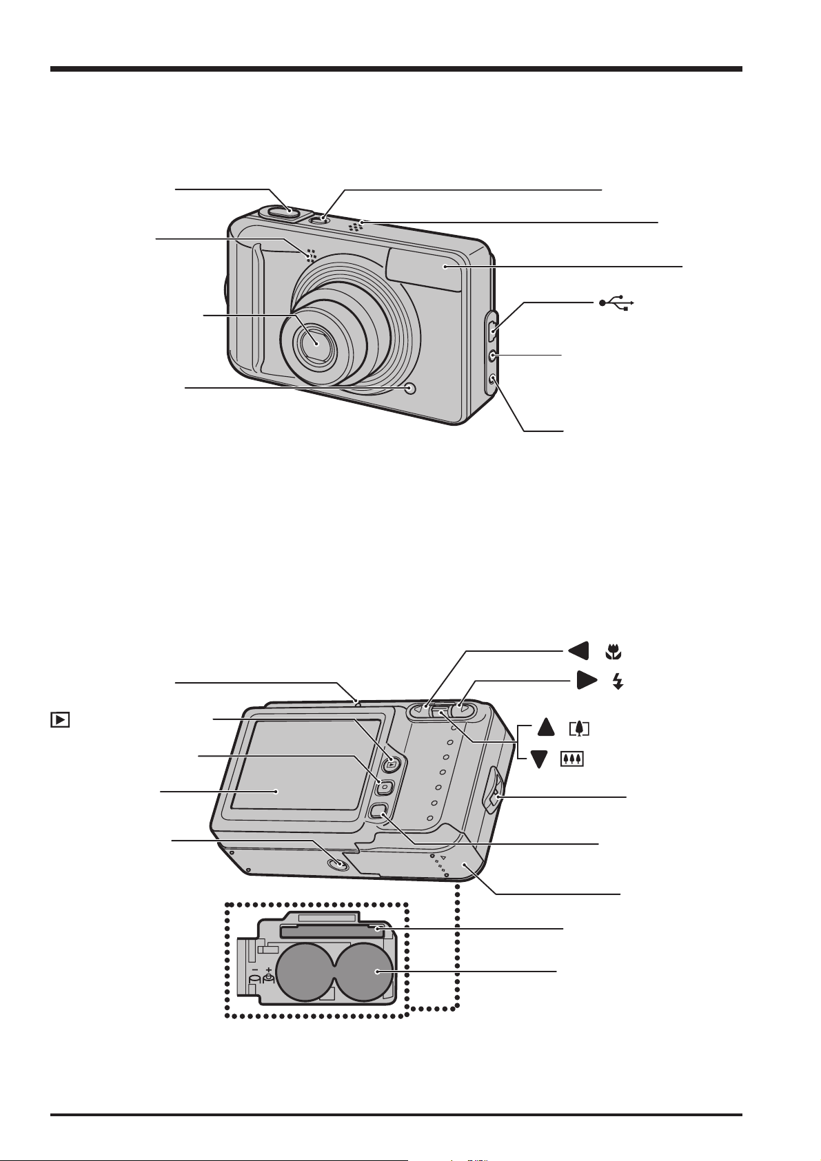
1-3. Names of External Components
FinePix A600 Service Manual
Shutter button
Microphone
Lens (lens cover)
Self-timer lamp
POWER button
Speaker
Flash
USB socket
(mini-B)
A/V OUT
(audio/visual output)
socket
DC IN 3V
(power input) socket
Indicator lamp
Playback button
MENU/OK button
LCD monitor
Tripod mount
DISP/
BACK
MENU
/OK
OPEN
/ Macro button
/ Flash button
/ Tele zoom switch
/ Wide zoom switch
Strap mount
DISP (display) /
BACK button
Battery cover
xD-Picture Card slot
Battery compartment
12
FinePix A600 Service Manual
2. Disassembly
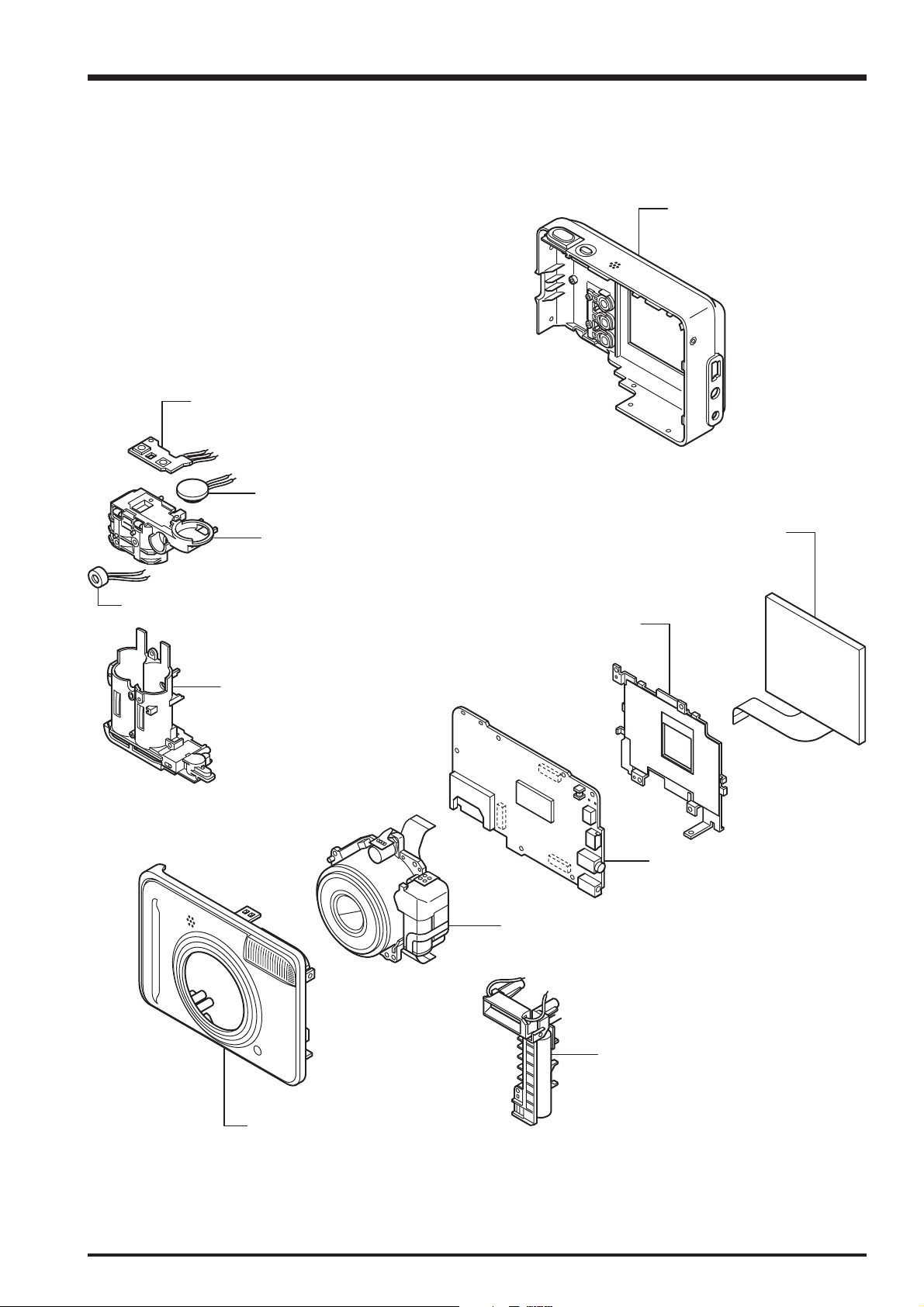
2-1. Names of internal Components
SUB PCB UNIT
SPEAKER
2. Disassembly
REAR COVER UNIT
MIC
REAR BATTERY BOX
FRONT BATTERY BOX
LCD
TFT HOLDER
MAIN PWB ASSY
LENS UNIT
FRONT COVER UNIT
FLASH UNIT
13
2. Disassembly
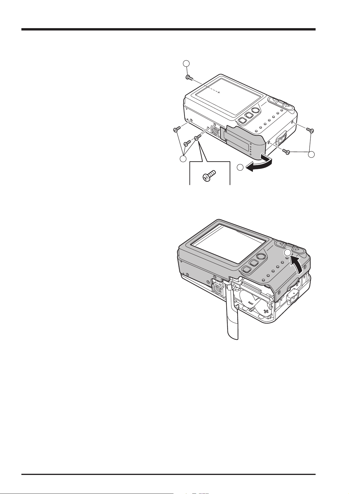
2-2. Removing the REAR COVER
FinePix A600 Service Manual
(1) Remove the 6 special screws (M1.7 x 5.0).
(2) Open the BATTERY COVER.
(3) Remove the REAR COVER in the direction of the
arrow.
1
1
2
1
[Assembly]
Assemble by performing the disassembly procedure in
reverse.
3
14
FinePix A600 Service Manual
2
1
6
2-3. Removing the LCD COVER
(1) Peel off the TFT HOLD SHEET.
(2) Raise the LCD in the direction of the arrow.
2. Disassembly
(3) Remove the 4 screws (M1.7 x 4.0).
(4) Remove the screw (M1.7 x 3.0).
(5) Remove the TFT HOLDER in the direction of the arrow.
(6) Remove the LCD FPC from the connector in the
direction of the arrow.
[Assembly]
Assemble by performing the disassembly procedure in
reverse.
3
5
4
15
2. Disassembly
2-4. Removing the SHUTTER BUTTON unit
FinePix A600 Service Manual
(1) Remove the POWER BUTTON and RELEASE
HOLDER connectors in the direction of the arrow.
(2) Remove the RELEASE HOLDER in the direction of the
arrow.
[Assembly]
Assemble by performing the disassembly procedure in
reverse.
2
1
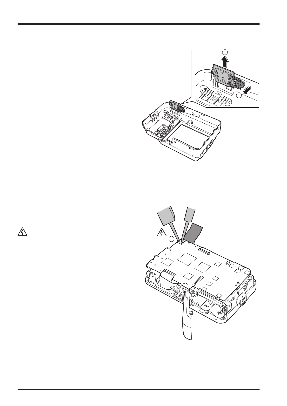
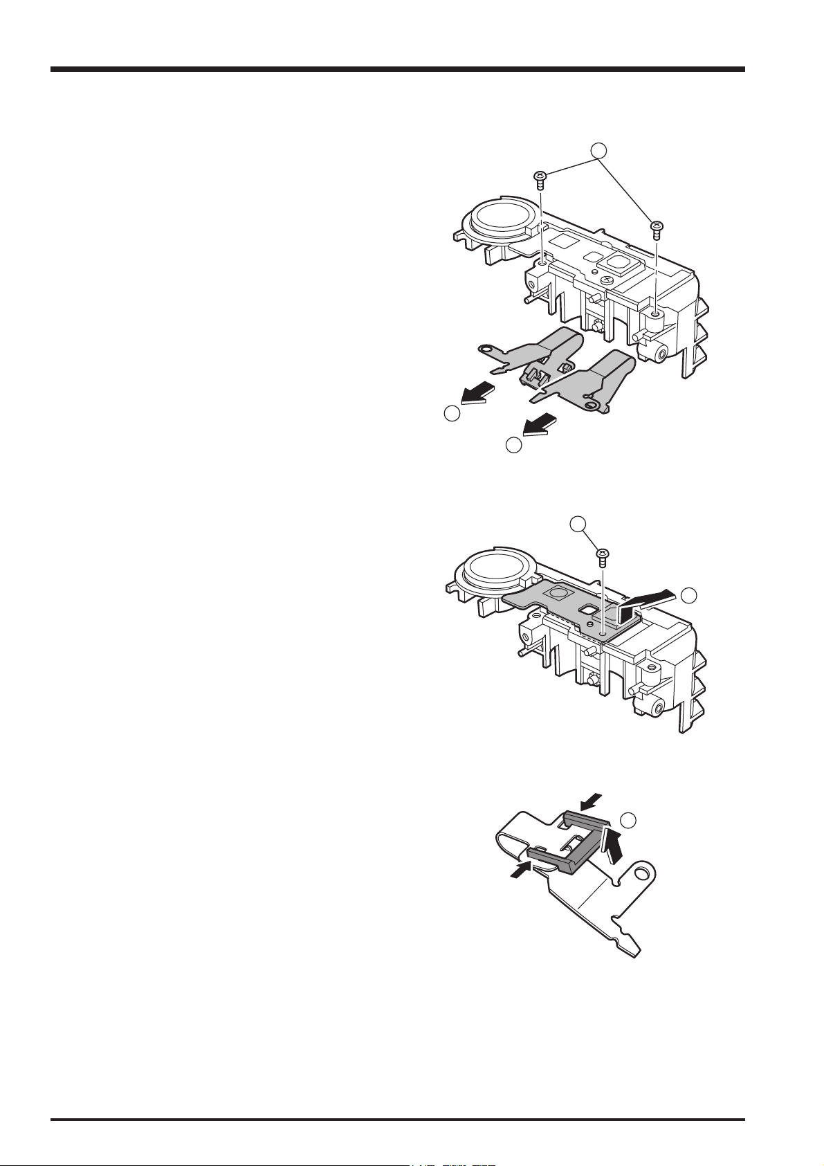
2-5. Removing the MAIN PWB ASSY
(1) Peel off the FLASH SHEET and discharge the main
capacitor.
Take care not to touch the main capacitor terminals
before discharging the capacitor.
1
16
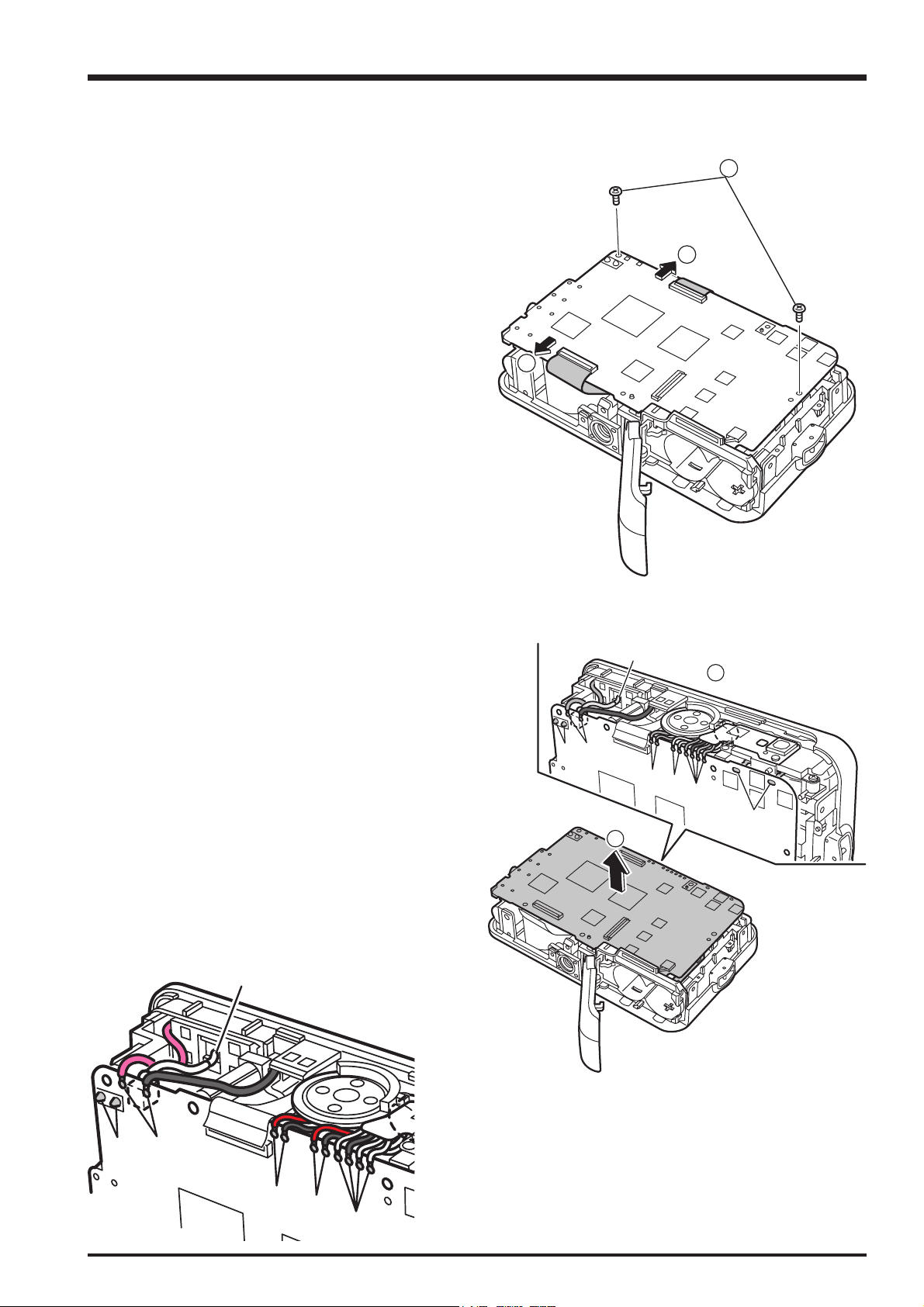
FinePix A600 Service Manual
2
3
4
(2) Remove the 2 screws (M1.7 x 3.0).
(3) Unlock the connector and remove the LENS FPC.
(4) Unlock the connector and remove the CCD FPC.
2. Disassembly
(F)
(G)
5
(C)
(B)
(A)
(D)
6
(5) A. Remove the solder on the 4 LEAD WIRES.
B. Remove the solder on the 2 MIC leads.
C. Remove the solder on the 2 SPEAKER leads.
D. Remove the BATTERY SP solder in 2 locations.
E. Remove the LEAD E. CAP solder in 2 locations.
F. Remove the solder on the 2 XE LEAD WIRES.
G. Remove the solder on the TRIGGER LEAD WIRE.
(6) Remove the MAIN PWB ASSY in the direction of the
arrow.
[Assembly]
Assemble by performing the disassembly procedure in
reverse.
(G)
(E)
(E)
(F)
(C)
(B)
(A)
17

2. Disassembly
2-6. Removing the LENS UNIT
FinePix A600 Service Manual
(1) Remove the 3 screws (M1.7 x 4.5).
(2) Remove the LENS UNIT in the direction of the arrow.
[Assembly]
Assemble by performing the disassembly procedure in
reverse.
1
2
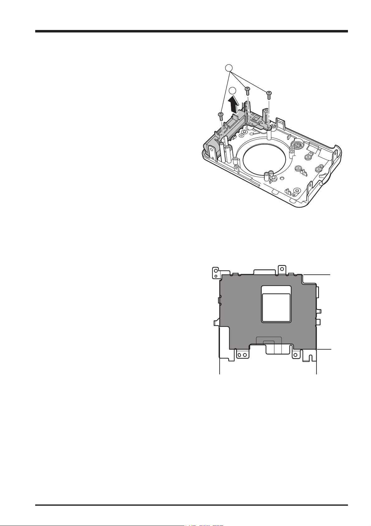
2-7. Removing the CCD
(1) Remove the 2 screws (M1.7 x 5.0).
(2) Remove the CCD PLATE.
(3) Remove the CCD FPC ASSY.
[Notes on Assembly]
Take care to ensure that no dust or soiling gets onto the
CCD FPC or LPF LENS.
[Notes on the OPTICAL LPF direction]
Assemble the OPTICAL LPF so that the IR-coated side
faces towards the CCD.
(The IR-coated surface is the side that appears red when
reflects light.)
[Assembly]
Assemble by performing the disassembly procedure in
reverse.
CCD PWB ASSY
LPF
RUBBER
OPTICAL
LPF
LPF
MASK
1
2
3
LENS UNIT
18

FinePix A600 Service Manual
5
6
2-8. Removing the BATTERY BOX
2. Disassembly
(1) Peel off the screening sheet.
(2) Remove the 2 screws (M1.7 x 3.0).
(3) Remove the BATTERY CASE F in the direction of the
arrow.
(4) Remove the BATTERY LID AXIS and then remove the
BATTERY LID.
2
1
3
4
(5) Remove the 2 screws (M1.7 x 3.0).
(6) Remove the BATTERY CASE R in the direction of the
arrow.
19
2. Disassembly
FinePix A600 Service Manual
(7) Remove the 2 screws (M1.7 x 3.0).
(8) Remove the BATTERY SP in the direction of the arrow.
(9) Remove the screw (M1.7 x 3.0).
(10) Remove the SUB PCB UNIT in the direction of the
arrow.
7
8
8
9
(11) Press both sides of the BATTERY FULL PROOF
gently towards the middle and then remove it in the
direction of the arrow.
[Assembly]
Assemble by performing the disassembly procedure in
reverse.
10
11
20
FinePix A600 Service Manual
2
1
2-9. Removing the FLASH UNIT
(1) Remove the 3 screws (M1.7 x 4.5).
(2) Remove the FLASH UNIT in the direction of the arrow.
[Assembly]
Assemble by performing the disassembly procedure in
reverse.
2. Disassembly
2-10. TFT SHEET installation location
Attach as shown in the figure on the right.
21

2. Disassembly
MEMO
FinePix A600 Service Manual
22

FinePix A600 Service Manual
3. Schematics
3. Schematics
3-1. Cautions
<Cautions when replacing parts>
• Do not reuse removed parts. Always use new parts.
• Note that the negative side of tantalum condensers is readily damaged by heat.
• Except for chemical condensers and tantalum condensers, voltage is not displayed on condensers with a voltage
resistance of 50V or less.
• Resistors not marked are 1/16W chip resistors.
•KΩ = 1000Ω, MΩ = 1000KΩ
• B characteristics of variable resistors and semi-fixed resistors are not displayed.
3-2. Basic Block Names and Functions
Part name Block name Function
LENS ASSY CCD BLOCK CCD output
MAIN PWB ASSY CAMERA BLOCK CCD output A/D conversion (IC103)
MOTOR BLOCK Shutter/Iris/AF/Zoom drive (IC501)
AUDIO BLOCK Audio IN/OUT (IC361)
VIDEO BLOCK Video output (IC207)
KEY BLOCK Key switch
FLASH BLOCK Flash charge, Flash firing
MEDIA BLOCK Media data IN/OUT
LCD BLOCK LCD output CN, Back light control
DCDC BLOCK Power supply generation (IC303), Flash charge control,
Power control
PROCESS BLOCK Image signal processing, USB communications,
system control (IC203)
SUB PWB ASSY SUB PWB BLOCK Release SW, Power SW
23

3. Schematics
FinePix A600 Service Manual
3-3. Functions of Primary Blocks
3-3-1. Technical Outline
Equipped with a 1/1.7-inch Super CCD HR (with 6.3 effective megapixels) and a Fujinon 3x optical zoom lens.
Features a image signal processing LSI chip, called the XCS2R_IC (IC203, CSP_IC), built into the MAIN PWB ASSY.
This CPU incorporates the standard peripheral I/O functions as well as the peripheral functions required for still image
processing into a single chip. Standard peripheral I/O consists of the interrupt controller, DMA controller, clock controller,
SDRAM controller, block selection controller, serial I/O, multifunction timer, monitoring timer, programmable I/O ports,
USB 2.0 (Full Speed), microprocessor ADC, microprocessor DAC, image processing circuit, JPEG compression/
expansion circuit, display control circuit, still image processing and card interface circuit.
In the white balance procedure, an algorithm has been installed that provides an estimation of the light source used for
shooting based on the brightness and light source color detected when the shot was taken, and a white balance (WB)
compensation function based on that estimation. The new algorithm is designed to prevent “hunting” due to field-of-view
slippage by providing more accurate brightness and color detection, and to allow the installation of a powerful algorithm
for distinguishing between the light source and the original subject colors.
Flash brightness is adjusted using the CCD-TTL method in which the flash brightness is calculated from the CCD
feedback data generated by the pre-flash.
Explanation of the imaging circuit functions
Analog video signals output from the CCD (1/1.7-inch with 6.3 effective megapixels) undergo pseudo-color correction
processing, adaptive interpolation processing, amplification and signal mixing in the BCS-R_IC (IC103; CSP_IC). The
converted digital signals are then sent to the single-chip image signal processing LSI chip, known as XCS2R_IC (IC203,
CSP_IC).
Input data from the CCD
* The 10-bit digital image data (corresponding to 1H) sent from the imaging circuit (BCS-R) is sent to XCS2R_IC, buffered
in the chip’s IBFC and replaced by 16-bit (96 MHz) data. The replaced 16-bit (96 MHz) image data is then stored in the
XCS2R_IC [SDRAM] via the XCS2R_IC [I/O BUFFER]. The image data for each frame is temporarily stored in the
XCS2R_IC [SDRAM].
* At the same time, the AE for [AUTO] is calculated using the 10-bit image data input to XCS2R_IC and the data required
for AE, AWB and AF is sent to the XCS2R_IC [SDRAM]. In the XCS2R_IC [SDRAM], the data is sent serially to AFE_CS
to obtain the correct AE, AWB and AF.
Recording onto an xD-Picture card
The image data stored in SDRAM is converted to 16-bit (96-MHz) data by [IBFC] in XCS2R_IC one line at a time and
then sent to [YC PRO]. In [IBFC], the 32-bit Y and C signals are each converted to 8-bit Y, Y, Cb and Cr signals and sent
to the XCS2R_IC [SDRAM]. The image data stored in the XCS2R_IC [SDRAM] is compressed using [JPEG] in
XCS2R_IC and then recorded sequentially onto the xD-Picture card via [MEDIA] in XCS2R_IC.
Playing back images from an xD-Picture card
The compressed image data from the xD-Picture card is sent to XCS2R_IC and stored in the XCS2R_IC [SDRAM] via
[MEDIA]. The compressed image data stored in the XCS2R_IC [SDRAM] is expanded using [JPEG] and again stored in
the XCS2R_IC [SDRAM]. The expanded image data is sent to [YC PRO] via [IBFC]. In [YC PRO], gain control and
aperture processing is applied for the brightness signals and color difference signals, after which the data is again stored
in the XCS2R_IC [SDRAM]. The image data is then displayed via [ENCD] and [D/A].
In movie shooting mode
The 10-bit digital image data output from the imaging unit is converted to 8-bit Y and C signals by the XCS2R_IC [YC
PRO] and sent to the XCS2R_IC [SDRAM]. The image data is compressed using [JPEG] in XCS2R_IC and again stored
in the XCS2R_IC [SDRAM]. The compressed data is then recorded sequentially onto the xD-Picture card via [MEDIA] in
XCS2R_IC.
The imaging system adjustment data is stored in FLASH_ROM (IC202).
Explanation of the LCD controller functions
The R, G and B signals processed in the XCS2R_IC image signal processor are output to the LCD panel via [LCD
CONST].
LCD Unit
The LCD monitor (1.8-inch 77,000 pixels) used in the camera uses a low-temperature polysilicon TFT color LCD screen.
Power Supply Section
Power supply circuits constructed in the core of the HPS_IC (IC303) create the following power supplies, which are
supplied to each block.
15V_CCD [IC102 (V_Drv), IC951 (CCD)]
5V_RUN [IC102 (V_Drv)]
-8V_CCD [IC102 (V_Drv), IC951 (CCD)]
3.3V_SYS [IC102 (V_Drv), IC103 (BCS-R), IC203 (XCS2R), IC361 (Audio Driver), IC501 (Motor Driver)]
3.3V_ RUN [IC501 (Motor Driver)]
3.3V_AOUT [IC203 (XCS2R), IC361 (Auido Driver)]
3.55V_RG [IC102 (V_Drv)]
1.5V_RUN [IC203 (XCS2R)]
24

FinePix A600 Service Manual
3. Schematics
3-4. Block Diagram
LENS ASSY
MOT_ZPLS
DC IN JACK
3.0V
BATT.
*R6x2
3xZOOM LENS
IRIS 2Steps
WIDE/TELE Variable
LENS Barrier
MOT_ZHP
MOT_FHP
3.3V
Motor Drv.
M63069HP
CTL
IC501
CSIO2
LED_ST_CAT
FLASH-XE
FLASH-C
FLASH_UNREG
FUSE
Thermal
Protector
Cont.
Pluse
15V
-8V
HA-CCD
MS3895D
MS3897
O.LPF
5V
MOT_SHT_MNS,MOT_SHT_MNS
Focus Pulse *3,Zoom Pulse *3
MOT_CS
VREF
FLASH
Block
LED
FET
LED
SELF TIMER
1/1.7inch
6.3million pixels
IC951
OFD
OFD/RG
BIAS
NJM2125F
IC101
3.3V
MD2174
IC102
LED
X’TAL
FC-255
32.768kHz
V Drv.
3.3V
IC303
Backup
ØV
V Pulse
LED
DRIVER
x 3
RTC
BATT
MAIN PWB ASSY
3.3V
IC103
CCDIN
ØH
FLASHCTRL
DC/DC Block
CCD 15V/-8.0V
BCS-R
3.3V Operation
CDS
CCDINCCDINCCDINCCDINCCDINCCDINCCDINCCDIN
H
Driver.
HPS
AN30202
+3.3VSYS
ADC
14bit
Digital
Gain
CSIO1
Power on
NEW
AD9996
Gray
Code
TG
(Programable)
CTL
Reset
FLASH_CHG
BATT V
+15V
-8V
+3.3V
HPS_CS
CSIO3
PWSW
RESET
CCD_DAT[9:0]
CAM_BCS_AVD,CAM_BCS_AHD,
CAM_BCS_ADCK
BCS_CS_N
CLOCK
Generator
BU3072HFV
CCDCLK_ON
IC205
27.0MHz/36.0MHz
CAM_CLK
VCLK_ON
IC204
CLOCK
Generator
48.00MHz
BU3073HFV
X’TAL
NX5032GA
48MHz
PWON ACT
XCS2R SIP
IBFC
RECC
YCPRO
zHM848MHz
CGEN
zHM212MHz
EVR
JPEG
NT/PAL_SW
24.545/24.375MHz
JTAG
XCS2-R 3.3V Operation
AUTO
CCDIF
MEDIA
TFDC
ENCD
M32R CPU Core
DEBUG I/F
CPU Core
I-cache 4k
BUS Cont.
SDRAMC
DMAC
CPU-A [10-11]
CPU_D[0-15]
(MAX 48MHz)
SDRAM
128MB x16
RESET
TESE
super AND FLASH MEMORY
HN29V 128A0A
IC202
16MByte
WDT
SIO
USB
MFT
ICU
ADC
PORT
CLKC
1.55V3.3V
IC203
LCDDAT[7:0]
LCD_HD,LCD_VD,LCDCLK
LCD_CS_N
Vbus,D+,D-
IO_AV_DET
VDO_OUT
VDO_ON
RLDU
MENU/OK
SUB PWB ASSY
RELEASE SW
xD Card
Slot
(20PIN)
CSIO2
POWER SW
DR_SW
IC207
Video
Driver
Audio
Driver
IC361
SDRAM
128MB x16
USER I/F
RLDU SW
MENU/OK
PLAY SW
DISP/BACK
V0.3.0V
3.3V
LCD
Cont.IC
LCD Panel
2.36inch
α-Si_TFT
BL LED x3
DCDC
USB I/F
VIDEO JACK
Mic
Spk
25

3. Schematics
3-5. Overall connection Diagram
FinePix A600 Service Manual
26
FinePix A600 Service Manual
3. Schematics
3-6. Circuit Diagrams
3-6-1. CAMERA BLOCK
27

3. Schematics
3-6-2. DCDC BLOCK
FinePix A600 Service Manual
28

FinePix A600 Service Manual
3. Schematics
3-6-3. MOTOR BLOCK
29

3. Schematics
3-6-4. PROCESS BLOCK
FinePix A600 Service Manual
30
 Loading...