YG862C10R (100V / 10A)
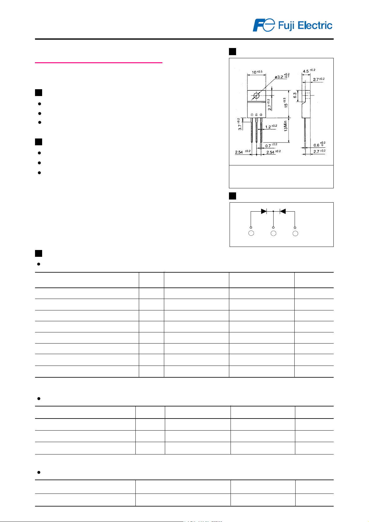
Outline drawings, mm
Low IR Schottky barrier diode
Features
Low IR
Low VF
Center tap connection
Applications
High frequency operation
DC-DC converters
AC adapter
Connection diagram
[200509]
Package : TO-220F
Epoxy resin UL : V-0
Maximum ratings and characteristics
Maximum ratings
Item
Repetitive peak surge reverse voltage
Repetitive peak reverse voltage
Isolating voltage
Average output current
Non-repetitive surge current
non-repetitive reverse surge power dissipation
Operating junction temperature
Storage temperature
Symbol
VRSM
VRRM
Viso
Io
IFSM
PRM
Tj
Tstg
Electrical characteristics (at Ta=25°C Unless otherwise specified )
Conditions
tw=500ns, duty=1/40
Terminals-to-Case, AC.1min.
Square wave, duty=1/2
Tc=118°C
Sine wave 10ms
tw=10µs, Tj=25°C
*
Out put current of center tap full wave connection
1
Rating
100
100
1500
10
125
330
+150
-40 to +150
32
Unit
V
V
V
*
A
A
W
°C
°C
Item
Forward voltage **
Reverse current **
Thermal resistance
Mechanical characteristics
Mounting torque
Approximate mass
http://www.fujielectric.co.jp/fdt/scd/
Symbol
V
F
IR
Rth(j-c)
Recommended torque
Conditions
IF=5A
VR=100V
Junction to case
Max.
0.86
150
3.5
0.3 to 0.5
2
Unit
V
µA
°C/W
**Rating per element
·m
N
g

(100V / 10A )
5
5
5
5
5
5
4
4
4
4
4
4
5
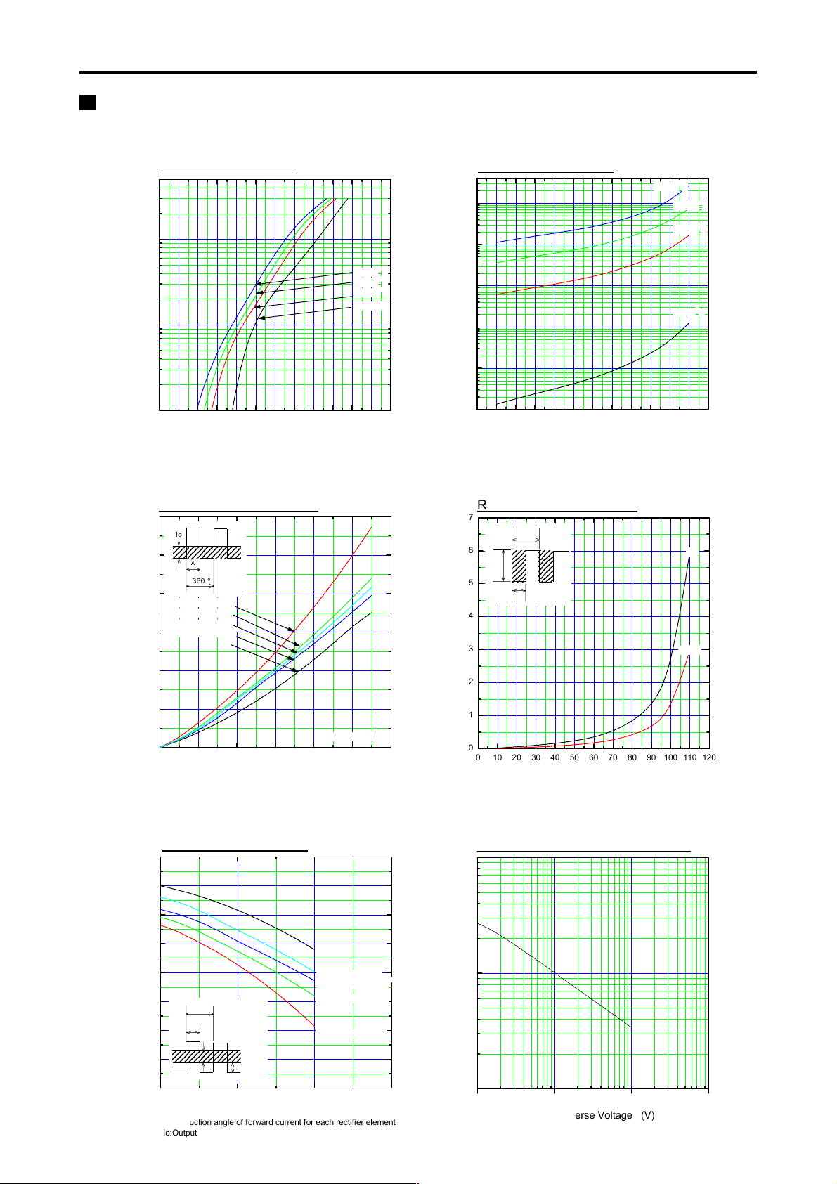
Characteristics
YG862C10R (10A)
Forward Characteristic (typ.)
10
1
IF Forward Current (A)
0.1
0.0 0.1 0.2 0.3 0.4 0.5 0.6 0.7 0.8 0.9 1.0 1.1 1.2
VF Forward Voltage (V)
Forward Power Dissipation (max.)
6
Io
2345678901234
5
λ
4
3
2
360 º
Square wave λ=60
Square wave λ=120
Sine wave λ=180
Square wave λ=180
DC
o
o
o
o
Tj=150oC
Tj=125oC
Tj=100oC
Tj=25oC
Reverse Characteristic (typ.)
1
10
0
10
-1
10
-2
10
-3
IR Reverse Current (mA)
10
-4
10
0 102030405060708090100110120
VR Reverse Voltage (V)
Reverse Power Dissipation (max.)
7
360 º
VR
23
234
23
234
23
234
23
234
23
234
23
α
6
5
4
3
2
Tj=150oC
Tj=125oC
Tj=100oC
Tj= 25oC
DC
α=180
o
1
WF Forward Power Dissipation (W)
0
0123456
Per 1element
Io Average Forward Current (A)
Current Derating (Io-Tc) (max.)
160
1
PR Reverse Power Dissipation (W)
0
0 102030405060708090100110120
VR Reverse Voltage (V)
Junction Capacitance Characteristic (max.)
1000
150
140
C)
o
130
120
110
100
Tc Case Temperature (
90
80
360 º
λ
Io
2345678901234
VR=50V
0 5 10 15
λ:Conduction angl e of forward current for each rectif ier element
Io:Output cur rent of center -tap full wave connection
Io Average Output Current (A)
DC
Sine wave λ=180
Square wave λ=180
Square wave λ=120
Square wave λ=60
o
o
o
o
100
Cj Junction Capacitance (pF)
10
1 10 100 1000
VR Reverse Voltage (V)
 Loading...