

Page 1

USER’S MANUAL
Instructions
series
(For SX-Programmer Expert [D300win]
Type: NP4H-SEDBV3)
FEH525a
Page 2

Preface
Thank you for purchasing Fuji Electric Programmable Controller MICREX-SX SPF Series.
This User’s Manual describes the memory specications and instructions dedicated to the SPF series.
Read this manual carefully to ensure correct operation and also read the corresponding user’s manuals listed below.
Title Manual No. Contents
User’s Manual Hardware,
MICREX-SX series SPF
User’s Manual Instructions (Expert),
MICREX-SX series SPH
User’s Manual Analog Unit,
MICREX-SX series SPF
User’s Manual Built-in High-Speed Counter,
MICREX-SX series SPF
User’s Manual
General Purpose Communication,
MICREX-SX series SPF
User’s Manual Pulse Output Instructions,
MICREX-SX series SPF
User’s Manual SX-Programmer Expert
(D300win) <Reference>, MICREX-SX series
* In addition to the above manuals, the following Fuji Electric Co.,Ltd.site offers various manuals and technical documents
associated with MICREX-SX series.
URL http://www.fujielectric.com
FEH526
FEH200
FEH527
FEH534
FEH528
FEH529
FEH257
Describes the system conguration, hardware specications and
operations of units in the MICREX-SX series SPF.
Describes the memory, language and system denitions of the
MICREX-SX series SPH (Expert).
Describes the specications and operations of analog input/output
units of the MICREX-SX series SPF.
Describes the specications and operations of the high-speed
counter built in the Main unit of the MICREX-SX series SPF.
Describes the specications of general purpose communication
(RS-232C/RS485) units/boards of the MICREX-SX series SPF
and how to create applications.
Describes the specications and operations of the high-speed
pulse output and high-speed positioning functions built in the
Main unit of the MICREX-SX series SPF.
Describes the functions and the operations of SX-Programmer
Expert (D300win) V3.
Notes
1. This manual may not be reproduced in whole or part in any form without prior written approval by the manufacturer.
2. The contents of this manual (including specifications) are subject to change without prior notice.
3. If you find any ambiguous or incorrect descriptions in this manual, please write them down (along with the manual No.
shown on the cover) and contact FUJI.
Page 3

Safety Precautions
: Incorrect handling of the device may result in minor injury or physical damage.
Be sure to read the "Safety Precautions" thoroughly before using the module.
Here, the safety precautions items are classied into "Warning" and "Caution".
Warning
: Incorrect handling of the device may result in death or serious injury.
Caution
Even some items indicated by "Caution" may result in a serious accident.
Both safety instruction categories provide important information. Be sure to strictly observe these instructions.
Warning
Neve touch any part of charged circuits as terminals and exposed metal portion while the power is turned ON.
It may result in an electric shock to the operator.
Turn OFF the power before mounting, dismounting, wiring, maintaining or checking, otherwise, electric shock, erratic
operation or troubles might occur.
Place the emergency stop circuit, interlock circuit or the like for safety outside the PLC. A failure of the PLC might break
or cause problems to the machine.
When using an expansion right side unit, be sure to mount a healthy unit to stop the SPF system with a fatal fault if the
expansion right side unit is dropped. Unless a healthy unit is mounted, a dropout of the expansion right side unit is not
detected and the SPF system continues operation in the state where the expansion right side unit is dropped.
Page 4

Safety Precautions
Caution
Do not use one found damaged or deformed when unpacked, otherwise, fire, failure or erratic operation might be caused.
Do not shock the product by dropping or tipping it over, otherwise, it might be damaged or troubled.
Follow the directions of the instruction manual and user’s manual when mounting the product.
If mounting is improper, the product might drop or develop problems or erratic operations.
Use the rated voltage and current mentioned in the instruction manual and user’s manual. Use beyond the rated values
might cause fire, erratic operation or failure.
Operate (keep) in the environment specified in the instruction manual and user’s manual. High temperature, high humidity,
condensation, dust, corrosive gases, oil, organic solvents, excessive vibration or shock, might cause electric shock, fire,
erratic operation or failure.
Select a wire size to suit the applied voltage and carrying current. Tighten the wire terminals to the specified torque.
Inappropriate wiring or tightening might cause fire, malfunction, failure or might cause the product to drop from its
mounting.
Contaminants, wiring chips, iron powder or other foreign matter must not enter the device when installing it, otherwise, fire,
accident, erratic operation or failure might occur.
Remove the dust-cover seals of modules after wiring, otherwise, fire, accident, erratic operation or failure might occur.
Connect the ground terminal to the ground, otherwise, electric shock or erratic operation might occur.
Periodically make sure the terminal screws and mounting screws are securely tightened.
Operation at a loosened status might cause fire or erratic operation.
Put the furnished connector covers on unused connectors, otherwise, erratic operation or failure might occur.
Sufficiently make sure of safety before program change, forced output, starting, stopping or anything else during a run.
Wrong operation might break or cause problems to the machine
Engage the loader connector in a correct orientation, otherwise, an erratic operation might occur.
Before touching the PLC, discharge any static electricity that may have been collected on your body. To discharge it, touch
a grounded metallic object. Static electricity might cause erratic operation or failure.
Be sure to install the electrical wiring correctly and securely, observing the directions of the instruction manual and user’s
manual. Wrong or loose wiring might cause fire, accident or failure.
When disengaging the plug from the outlet, do not pull the cord, otherwiase, break of cable might cause fire or failure.
Do not attempt to change system configurations (such as installing or removing expansion block) while the power is ON,
otherwise, failure or erratic operation might occur.
Do not attempt to repair the module by yourself, but contact your Fuji Electric agent, otherwise, fire, accident or failure
might occur.
To clean the module, turn power off and wipe the module with a cloth moistened with warm water. Do not use thinner or
other organic solvents, as the module surface might become deformed or discolored.
Do not remodel or disassemble the product, otherwise, failure might occur.
Follow the regulations of industrial wastes when the device is to be discarded.
The products covered in this user’s manual have not been designed or manufactured for use in equipment or systems
which, in the event of failure, can lead to loss of human life.
Do not use the products covered in this user’s manual for special applications, such as power plant, radiation facilities,
railroad, space/flight equipments, lifeline facilities, or medical equipments, where a great effect on human life, body,
society, major property or rights may be anticipated and high degree of safety is required.
Be sure to provide protective measures when using the products covered in this manual in equipment which, in the event
of failure, can lead to loss of human life or other grade results.
External power supply (such as 24 V DC power supply) which is connected to DC I/O should be strongly isolated from AC
power supply, otherwise, accident or failure might occur. (Use of EN60950 conforming power supply is recommended.)
Do not use the peoducts covered in this user’s manual in a residential environment.
Page 5

Revision
* The manual No. is printed at the bottom right of the cover of this manual.
Printed on * Manual No. Revision contents
Mar. 2017 FEH525 First edition
Dec. 2017 FEH525a • The following sub sections were added.
“1-3-8 (9) and (10),” and “1-10.”
• R_READ, R_WRITE and C_ETHERNET FBs were added to “2-3-2 (4) Function block
summary.”
Page 6

Contents
Preface
Safety Precautions
Revision
Contents
Section 1 Specications
1-1 Performance Specications ...............................................................................................................1-1
1-2 Function Specications ......................................................................................................................1-3
1-3 Memory ..............................................................................................................................................1-4
1-3-1 Memory map .................................................................................................................................................1-4
1-3-2 Input/output memory area .............................................................................................................................1-6
1-3-3 Standard memory area .................................................................................................................................1-7
1-3-4 Retain memory area......................................................................................................................................1-8
1-3-5 User FB instance memory area ....................................................................................................................1-9
1-3-6 System FB instance memory area ................................................................................................................1-10
1-3-7 System memory area ....................................................................................................................................1-11
1-3-8 SPF original special relay/register area ........................................................................................................1-22
1-4 I/O Address Assignment ..................................................................................................................... 1-40
1-4-1 Rules for assigning I/O addresses ................................................................................................................1-40
1-4-2 Example of address assignment ...................................................................................................................1-40
1-5 Variables ............................................................................................................................................. 1-42
1-5-1 Overview of variables ....................................................................................................................................1-42
1-5-2 Variable declaration .......................................................................................................................................1-43
1-6 Data Types .........................................................................................................................................1-47
1-6-1 Organization of data types ............................................................................................................................1-47
1-6-2 Basic data types ............................................................................................................................................1-48
1-6-3 Derived data types ........................................................................................................................................1-50
1-7 Tasks ..................................................................................................................................................1-55
1-7-1 Task specications ........................................................................................................................................1-55
1-7-2 Types and operations of tasks ......................................................................................................................1-55
1-7-3 Example of xed cycle task operation ...........................................................................................................1-56
1-7-4 Example of event task operation ...................................................................................................................1-57
1-8 Program Organization Units (POUs) ..................................................................................................1-58
1-9 Calendar Function ..............................................................................................................................1-61
1-9-1 Calendar value range ....................................................................................................................................1-61
1-9-2 Calendar accuracy ........................................................................................................................................1-61
1-9-3 How to monitor and set the calendar from D300win .....................................................................................1-61
1-9-4 How to monitor and set the calendar from an application program...............................................................1-62
1-10 Writing/Reading Data to/from Memory Pack ....................................................................................1-63
Section 2 Programming Languages
2-1 Types of Programming Languages .................................................................................................... 2-1
2-2 LD Language ......................................................................................................................................2-2
2-2-1 LD language ..................................................................................................................................................2-2
2-3 FBD Language ...................................................................................................................................2-3
2-3-1 Function summary.........................................................................................................................................2-4
2-3-2 Function block summary ...............................................................................................................................2-28
2-3-3 SPF Original FCTs ........................................................................................................................................2-41
2-4 ST Language ......................................................................................................................................2-43
2-4-1 ST operators .................................................................................................................................................2-43
Page 7

Contents
2-4-2 ST statements ...............................................................................................................................................2-44
2-5 IL Language .......................................................................................................................................2-45
2-5-1 IL instruction summary ..................................................................................................................................2-45
2-6 SFC Elements ....................................................................................................................................2-48
2-6-1 SFC elements ...............................................................................................................................................2-49
2-6-2 Step transition ...............................................................................................................................................2-57
2-6-3 Automatically generated SFC variables ........................................................................................................2-60
2-6-4 SFC programming precautions .....................................................................................................................2-61
2-6-5 Continuous operation of SFC ........................................................................................................................2-62
Section 3 System Denition
3-1 System Denition Summary ...............................................................................................................3-1
3-2 System Conguration Denition .........................................................................................................3-2
3-2-1 System conguration denition .....................................................................................................................3-2
3-3 Parameters for Main Unit ...................................................................................................................3-4
3-3-1 CPU running denition ..................................................................................................................................3-4
3-3-2 CPU memory size denition ..........................................................................................................................3-6
3-3-3 I/O group setting............................................................................................................................................3-8
3-3-4 Remote RUN/STOP bit setting ......................................................................................................................3-10
3-3-5 Digital lter setting .........................................................................................................................................3-11
3-3-6 High-speed counter setting ...........................................................................................................................3-12
3-3-7 High-speed pulse output setting....................................................................................................................3-13
Page 8

Section 1 Specications
1-1 Performance Specications ................................................................... 1-1
1-2 Function Specications ..........................................................................1-3
1-3 Memory .....................................................................................................1-4
1-3-1 Memory map ..................................................................................................1-4
(1) Main unit with 14/24 points ............................................................................1-4
(2) Main unit with 32/40/60 points .......................................................................1-5
1-3-2 Input/output memory area ..............................................................................1-6
1-3-3 Standard memory area ...................................................................................1-7
1-3-4 Retain memory area .......................................................................................1-8
1-3-5 User FB instance memory area ......................................................................1-9
1-3-6 System FB instance memory area ...............................................................1-10
1-3-7 System memory area ................................................................................... 1-11
(1) System memory ........................................................................................... 1-11
(2) Resource operating status %MW10.0 (Read only) ....................................1-12
(3) Resource switch / User ROM state %MW10.1 (Read only) ......................1-12
(4) Resource fatal fault factor %MW10.2 (Read only) .....................................1-13
(5) Resource nonfatal fault factor %MW10.4 (Read only) ...............................1-13
(6) CPU error factor %MW10.6 (Read only) ...................................................1-13
(7) Memory error factor %MW10.8, %MW10.9 (Read only) ...........................1-14
(8) Application error factor %MW10.12, %MW10.13 (Read only) ...................1-14
(9) User fatal fault %MW10.14 to %MW10.16 ................................................1-15
(10) User nonfatal fault %MW10.18 to %MW10.20 ........................................1-15
(11) System denition error factor %MW10.22 to %MW10.27
(Read only) ................................................................................................1-16
(12) Application program error factor %MW10.38 to %MW10.41 ................... 1-17
(13) Announce relay %MW10.42, %MW10.43 (Read only) ............................1-18
(14) Resource running information %MW10.49 (Read only) ..........................1-19
(15) Resource conguration/fault information %MW10.50, %MW10.51
(Read only) ................................................................................................1-19
(16) Conguration/conguration fault information %WM10.52 to %WM10.83
(Read only) ................................................................................................1-20
(17) User ROM status %MW10.298 (Read only) ............................................1-21
(18) SPF original announce relay %MW10.299 (Read only) ..........................1-21
1-3-8 SPF original special relay/register area ........................................................1-22
(1) Built-in calendar data %MW1.61442 to %MW1.61449 ..............................1-22
(2) Battery information %MW1.61450 .............................................................1-22
(3) Pulse catch input %MW1.61472 to %MW1.61479 ....................................1-22
(4) Memories related to interrupt %MW1.61480 to %MW1.61498 ..................1-23
(5) Memories related to high-speed counter
%WM1.61536 to %WM1.61561, %WM3.61536 to %WM3.61577 .............1-25
(6) Memories related to pulse/positioning
%MW1.61600 to %MW1.61769, %MW3.61600 to %MW3.61613 ..............1-27
Page 9

(7) Memories related to general purpose communication
%MW1.61793 to %MW1.61838 ................................................................... 1-31
(8) Memories related to CPU link %MW1.61858 to %MW1.62399 .................1-33
(9) Memories related to Ethernet
%MW1.62400 to %MW1.62463, %MW3.62400 to %MW3.62463 ..............1-35
(10) Data write/read parameter for memory pack
%MW3.61440 to %MW3.61471 ................................................................1-39
1-4 I/O Address Assignment ....................................................................... 1-40
1-4-1 Rules for assigning I/O addresses ...............................................................1-40
(1) Unit No. ........................................................................................................1-40
(2) Word No. and bit address ............................................................................ 1-40
1-4-2 Example of address assignment ..................................................................1-40
(1) Example of a system consisting only of a main unit (40 points) ..................1-40
(2) Example of a system in which expansion units are connected to
a main unit (60 points) .................................................................................1-41
(3) Example of a system in which expansion units are connected to
a main unit (32 points) .................................................................................1-41
1-5 Variables .................................................................................................1-42
1-5-1 Overview of variables ...................................................................................1-42
1-5-2 Variable declaration ......................................................................................1-43
(1) Usage of variables .......................................................................................1-43
(2) Assigning variables to memory ....................................................................1-44
(3) Retaining variables during power failure ......................................................1-46
(4) Setting initial value for variable ....................................................................1-46
(5) Restrictions on variable names ....................................................................1-46
1-6 Data Types .............................................................................................1-47
1-6-1 Organization of data types ...........................................................................1-47
1-6-2 Basic data types ...........................................................................................1-48
1-6-3 Derived data types .......................................................................................1-50
(1) Array data types ...........................................................................................1-50
(2) Structured data types ...................................................................................1-52
(3) Restrictions on derived data types ...............................................................1-54
1-7 Tasks ...................................................................................................... 1-55
1-7-1 Task specications .......................................................................................1-55
1-7-2 Types and operations of tasks ......................................................................1-55
1-7-3 Example of xed cycle task operation ..........................................................1-56
1-7-4 Example of event task operation ..................................................................1-57
1-8 Program Organization Units (POUs) ...................................................1-58
1-9 Calendar Function .................................................................................1-61
1-9-1 Calendar value range ...................................................................................1-61
1-9-2 Calendar accuracy .......................................................................................1-61
1-9-3 How to monitor and set the calendar from D300win ....................................1-61
1-9-4 How to monitor and set the calendar from an application program .............. 1-62
1-10 Writing/Reading Data to/from Memory Pack ....................................1-63
Page 10

Section 1 Specications
1-1 Performance Specications
Item
Control system
I/O connection method Direct input/output (local bus)
I/O control system
CPU 16-bit processor
Memory types Program memory, data memory, temporary memory
Programming language
Length of instructions Variable length (depending on language)
Instruction execution
speed
Program memory capacity (Note 2) 8192 steps 20480 steps
Program steps in a POU 8192 steps 16384 steps
Sequence instruction Contact: mini. 0.30 µs, Coil: min. 0.33 µs
Applied instruction Timer: min. 10.06 µs, Counter: min. 7.51 µs
Specication
Main unit with 14/24 points Main unit with 32/40/60 points
Stored program,
Cyclic scanning system (default task), xed cycle task, event task
Whole: Scan batch refresh system
Digital I/O: Task synchronized refresh system
IL language, (Instruction List)
ST language (Structured Text)
LD language, (Ladder Diagram)
FBD language, (Function Block Diagram)
SFC language, (Sequential Function Chart) Adhere to IEC61131-3
I/O memory (I/Q) 512 words
Standard memory (M) 4096 words 8192 words
Retain memory (M) 2048 words 4096 words
User FB instance memory 4096 words 8192 words
User FB instance memory
Initial value setting memory
Memory
(Note 1)
Temporary area 8192 words
Available basic data type (Note 3)
System FB
instance
memory
System memory (M) 512 words
Special relay/register (non-retain) (M) 4096 words
Special relay/register (retain) (L) 4096 words
Timer 256 points 512 points
Additional timer 0 point 0 point
Counter 256 points 512 points
Edge detection 1024 points 2048 points
Others 512 words 1024 words
4608 words 9216 words
5632 words 11264 words
BOOL, INT, DINT, UINT, UDINT, REAL,TIME, DT, DATE, TOD, WORD,
DWORD
Data type nesting
Notes:
1) You can freely increase or decrease the area sizes of the standard memory, retain memory, user FB instance memory, and
system FB instance memory. The above table shows the default values.
2) The initial value setting area of the standard memory and retain memory is included.
3) Available data types depend on the instruction.
One level
(array of arrays, structure of arrays, array of structures, structure of structures)
1-1
Page 11
Section 1 Specications
Item Specication
No. of structure data type members 200
Max. No. of elements of array data type 16-bit data type: 4096, 32-bit data type: 2048
No. of tasks
Program instance (No. of POUs / task)
No. of user function blocks 128
No. of user functions 128
Nesting depth of user function blocks / user
functions
Variable
No. of user FB terminals
Library
Global variable 15000
Local variable 15000/POU
No. of registered libraries 16/project
Nesting depth 8 levels
Default tasks (Cyclic scanning): 1
Fixed cycle tasks + Event tasks: 15 in total
64 / Default task
8 / Fixed cycle task, Event task
(Total of all tasks: Max. 64)
64 levels in total
(Including user function blocks / user functions called from a program)
VAR_INPUT : Up to 128
VAR_OUTPUT : Up to 128
128 in total
1-2
Page 12

Section 1 Specications
1-2 Function Specications
Item Main unit specication
External interrupt input function Max. 16 points (rising edge / falling edge / rising and falling edges)
Pulse catch function
No. of channels Max. 8 channels (single phase)
High-speed
counter
0.1 ms high-speed timer When using high-speed counter in high-speed timer mode
High-speed
pulse output
and
High-speed
positioning
Communication
port
Diagnostic function Self-diagnosis (memory check, ROM sum check), system conguration supervising
Security function Password (Set by the support tool)
Count frequency
Count mode U/D, U/D × 2, P/R, P/R × 2, A/B, A/B × 2, A/B × 3, A/B × 4 (Note 1)
No. of axes Max. 4
Output frequency Max. 200kHz
Output pulse mode U/D, P/R, A/B, PLS, PWM (Note 1) (Note 2)
Pulse output instruction By SPF original instructions
PORT0 (RS232C) Loader port built in main unit
PORT1, PORT2
(Communication board)
PORT3, PORT4
(Communication unit)
Max. 36 points (rising edge / falling edge)
Max. 200kHz (Advance Main unit)
Max. 100kHz (Basic Main unit)
Communication mode:
Loader communication, general-purpose communication, CPU link communication
(only one port among them),
Modbus RTU master communication
Transmission speed:
1200/2400/4800/9600/19200/38400/57600/115200 bps
Calendar function
Program memory,
system denition
Backup
(Note 3)
User ROM function
Notes:
1) U/D: Up/Down pulse mode, P/R: Pulse / Direction signal mode, A/B: A/B phase mode, x2: 2 multiplication, x3: 3 multiplication,
x4: 4 multiplication
2) PLS: Single pulse output mode, PWM: PWM output mode
3) The backup time is 10 years or more (ambient temperature: 55°C)
4) Notes on rewriting programs
When rewriting the program in the main unit from the loader while the PLC is running, the built-in RAM is changed, however,
the built-in ash memory is unchanged. As a result, the contents of the RAM does not match those of the ash memory, and
the RUN/MEM LED blinks to prompt the user to transfer the contents of the RAM to the ash memory.
After rewriting the program, be sure to transfer the contents of the RAM to the ash memory. When the transfer is completed
normally, the RUN/MEM LED turns OFF.
<Method 1>
By using the loader, transfer the contents of the RAM to the ash memory.
<Method 2>
After rewriting the program, turn OFF the main unit and then ON again. When the power supply is turned ON, the contents
of the RAM is automatically transferred to the ash memory.
ZIP le Built-in ash memory
Data memory Built-in RAM: Built-in lithium primary battery
Calendar Calendar IC: Built-in lithium primary battery
Available up to 31 Dec. 2069 23:59:59
Precision: ±20 sec/day (at 25°C)
Built-in RAM: Built-in lithium primary battery
Built-in ash memory (Note 4)
Programs, system denitions, and zipped les can be stored in the external memory
pack (NA8PMF-20).
1-3
Page 13

Section 1 Specications
IEC representation
1-3 Memory
1-3-1 Memory map
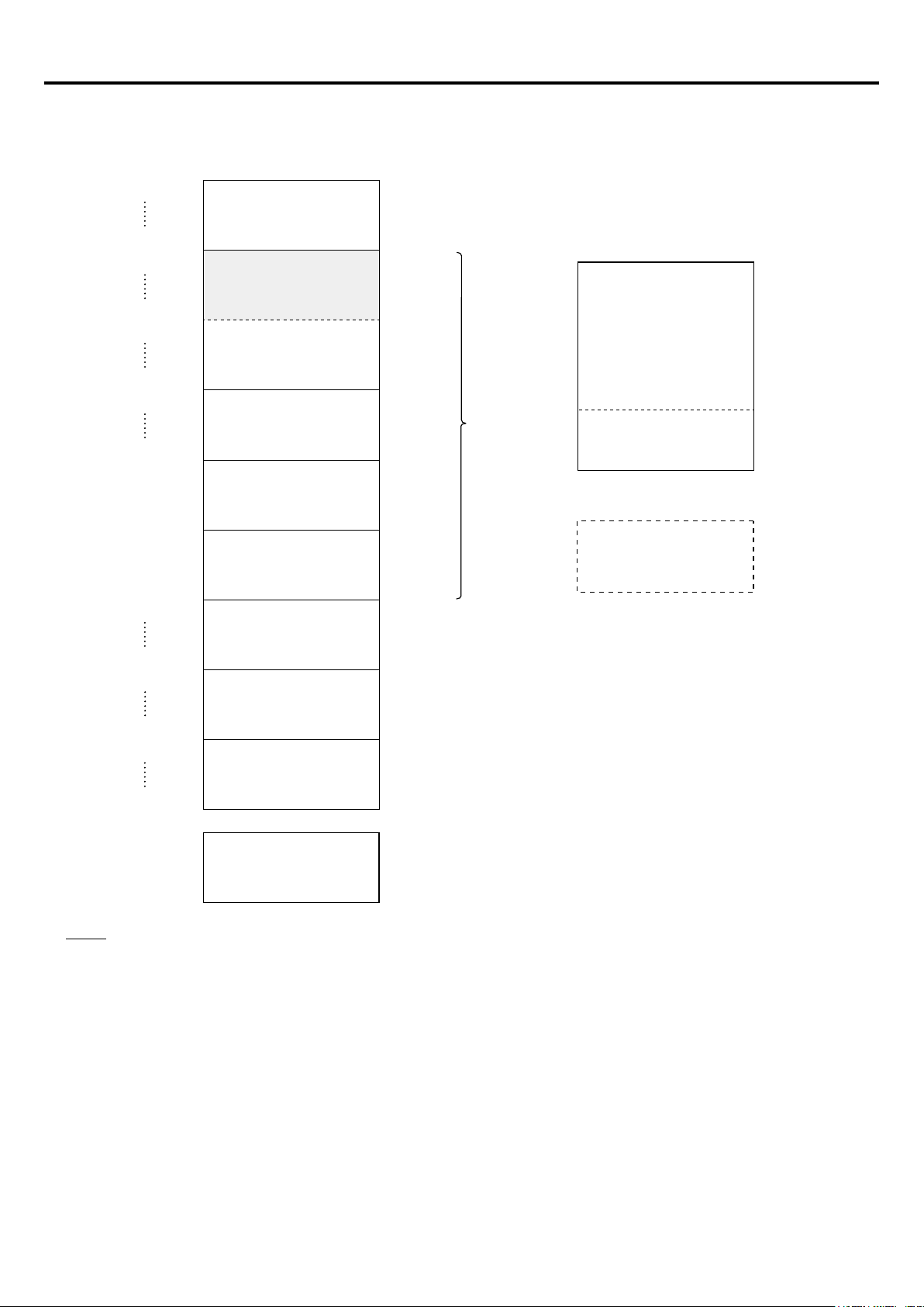
(1) Main unit with 14/24 points
(Input) (Output)
%I %Q
Input/output memory
(I/Q)
512 words (8192 points)
(Note 3)
%MW1.0
%MW1.4095
%MW3.0
%MW3.2047
%MW10.0
%MW10.511
%MW1.61440
Standard memory
(High-speed)
(M)
4K words
Standard memory
(M)
0K word
Retain memory
(M)
2K words
User FB instance memory
4K words
System FB instance memory
5.5K words
System memory
(M)
512 words
Special relay/register
(non-retain) (M)
4K words
(Note 2)
(Note 1)
Program memory
8K steps
Initial value setting area
for standard memory and
retain memory (Note 4)
Temporary area
8K words
* 1K = 1024
%MW3.61440
Special relay/register
(retain) (M)
4K words
User FB instance memory
Initial value setting memory
4.5K words
(Note 5)
Notes:
1) You can increase or decrease the size of the standard memory (excluding high-speed memory), retain memory, user FB
instance memory, and system FB instance memory by the loader. The default values are shown in the gure above. For
details, see “3-3-2 CPU memory size denition.”
2) The rst 4K words of the standard memory (M) are used as a high-speed memory for high-speed access. You cannot
change the size.
3) For the input/output address assignment, see “1-4 I/O Address Assignment.”
4) You can set the initial values of the standard memory and retain memory using the free space of the program memory.
Initial values require 2.5 steps per variable.
5) The initial value setting memory is automatically allocated according to the size of the user FB instance memory and uses
he area of user FB memory x 1 1/8 words.
1-4
Page 14
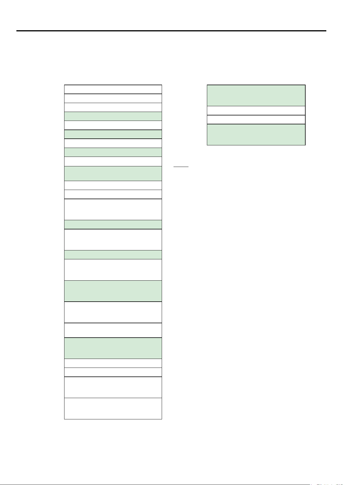
Section 1 Specications
IEC representation
(2) Main unit with 32/40/60 points
(Input) (Output)
%I %Q
Input/output memory
(I/Q)
512 words (8192 points)
(Note 3)
%MW1.0
%MW1.4095
%MW1.4096
%MW1.8191
%MW3.0
%MW3.4095
%MW10.0
%MW10.511
%MW1.61440
Standard memory
(High-speed)
(M)
4K words
Standard memory
(M)
4K words
Retain memory
(M)
4K words
User FB instance memory
8K words
System FB instancememory
11K words
System memory
(M)
512 words
Special relay/register
(non-retain) (M)
4K words
(Note 2)
(Note 1)
Program memory
20K steps
Initial value setting area
for standard memory and
retain memory (Note 4)
Temporary area
8K words
* 1K = 1024
%MW3.61440
Special relay/register
(retain) (M)
4K words
User FB memory
Initial value setting memory
9K words
(Note 5)
Notes:
1) You can increase or decrease the size of the standard memory (excluding high-speed memory), retain memory, user FB
instance memory, and system FB instance memory by the loader. The default values are shown in the gure above. For
details, see “3-3-2 CPU memory size denition.”
2) The rst 4K words of the standard memory (M) are used as a high-speed memory for high-speed access. You cannot
change the size.
3) For the input/output address assignment, see “1-4 I/O Address Assignment.”
4) You can set the initial values of the standard memory and retain memory using the free space of the program memory.
Initial values require 2.5 steps per variable.
5) The initial value setting memory is automatically allocated according to the size of the user FB instance memory and uses
the area of user FB memory x 1 1/8 words.
1-5
Page 15

Section 1 Specications
IEC representation
15……………………………0
………………………………………
1-3-2 Input/output memory area
The input/output memory area is a window through which data are exchanged between the main unit (user application) and
external devices. This area is used by input devices such as pushbuttons, switches, and sensors which send data to the main
unit and by output devices such as relays, solenoids, and indicators which show the results of program executions.
Key points:
G
1) Input is represented by %I (prex), and output by %Q (prex). When actually assigning an I/O address, these prexes
are followed by a size and address in the variable declaration. For details, see “1-4 I/O Address Assignment.”
2) Both input and output cannot exist in the same word.
%I %Q
Input/output memory
512 words
1-6
Page 16

Section 1 Specications
15……………………………0IEC representation
1-3-3 Standard memory area
The standard memory area is used for auxiliary relays that are used internally in the PLC.
Key points:
G
1) In the direct addressing mode, this memory area is specied in he format of %Mo1. ... (replace o with any of X, W, or D).
Usually, since a variable declaration is used to assign memory to an application program, you may neglect addresses in
programming. See “1-5 variables” for details.
2) The specied memory area is reset to (0) zero when self-PLC is started.
3) 4K words from the top of the standard memory is the area where data access in the CPU is processed at high speed.
4) The sizes of the standard memory areas can be changed taking those of other areas into account. Note that the size of
the high-speed access memory area is xed to 4K words and cannot be changed.
For the details of memory size change, see “3-3-2 CPU memory size denition.”
5) No continuous access is allowed to the high-speed access memory area and the boundaries between other areas.
For example, an array or structure cannot lie across the boundary
%MW1.0
%MW1.4095
%MW1.4096
……………………………… ……
Standard memory
(high speed)
(M)
4K words
Standard memory
(M)
Unit with 14/24 points
: 0K word
Unit with 32/40/60 points
: 4K words
1-7
Page 17

Section 1 Specications
15……………………………0
IEC representation
1-3-4 Retain memory area
The retain memory area is used for the auxiliary relays that are used internally in the PLC.
Key points:
G
1) In the direct addressing mode, this memory area is specied in he format of %Mo3. ... (replace o with any of X, W, or D).
Usually, since a variable declaration is used to assign memory to an application program, you may neglect addresses in
programming. see “1-5 variables” for details.
2) The following processes are performed at cold or warm start.
Cold start Warm start
(Note)
Standard memory Reset to 0 (zero).
Initialized standard memory Writes specied initial values.
3) You can select whether or not to clear this area when transferring the project.
If you select “clear,” the system cold-starts and If “not clear,” the system warm-starts.
4) The size of the retain memory area can be changed taking those of other areas into account.
For the details of memory size change, see “3-3-2 CPU memory size denition.”
%MW3.0
……………………………………………
Retain memory
(M)
Unit with 14/24 points
: 2K words
Unit with 32/40/60 points
: 4K words
Retains old values.
Retains old values.
Notes:
1) The CPU runs in “cold start” mode when started by the “Initial run” command of the loader and in “warm start” mode when
the system power is turned ON or started by the “Run” command of the loader.
2) In the following cases, the PLC cold-starts.
• When started up for the rst time after user ROM with different memory allocation was installed
• When started up for the rst time after memory backup error occurred
• When started up for the rst time after the resources were initialized
• When started up for the rst time after the data memory in this area was cleared
• During battery-less operation
1-8
Page 18

Section 1 Specications
1-3-5 User FB instance memory area
The user FB instance memory area is an instance memory area dedicated to each user FB used internally in the PLC.
Key points:
G
1) The size of the user FB instance memory area can be changed taking those of other areas into account.
For the details of memory size change, see “3-3-2 CPU memory size denition.”
2) When setting an initial value in the user FB internal memory, “No. of words in user FB instance area that are dened in
the variable worksheet” x 9/8 is required for the user FB initial value setting area.
3) You can select whether or not to clear the memory for saved attributes in this area when transferring the project.
User FB
instance memory
Unit with 14/24 points
: 4K words
Unit with 32/40/60 points
: 8K words
Notes:
The default values are shown in the left gure.
1-9
Page 19

Section 1 Specications
1-3-6 System FB instance memory area
The user FB memory area is a real memory area dedicated to the system FBs such as timers, counters, and differential
instructions that are used internally in the PLC.
Key points:
G
1) At PLC startup, predened initialization is performed. (the old values are retained or reset to 0s (zeros).
Example) The current values for the counters and additional timers and the old value for the edge detect instruction
counter are retained, while the current values for the timers (excluding additional) are reset to 0s (zeros).
2) Eight words/timer, four words/counter, and two words/edge detect instruction counter are used.
3) The size of the system FB instance memory area can be changed taking those of other areas into account.
For the details of memory size change, see “3-3-2 CPU memory size denition.”
4) By default, the numbers of timers, additional timers, counters, and edge detect instruction counters have been preset
per main unit. If necessary, you can change these numbers.
Timer
Main unit with 14/24 points 256 points 0 point 256 points 1024 points 512 words
Main unit with 32/40/60 points 512 points 0 point 512 points 2048 points 1024 words
To set the timer, additional timer, counter, edge detect, and other system FB areas, the following conditions must be
met.
(No. of timers) × 8 words + (No. of counters) × 4 words + (No. of edge detect counters) × 2 words + Others
<= Preset size of system FB instance memory area
5) You can select whether or not to clear the memory for saved attributes in this area when transferring the project.
Additional
timer
Counter Edge detect Others
1-10
Page 20
Section 1 Specications
1-3-7 System memory area
The use of the system memory is predetermined; the ags to indicate the operating status and error condition of the MICREX-SX
SPF series system are allocated.
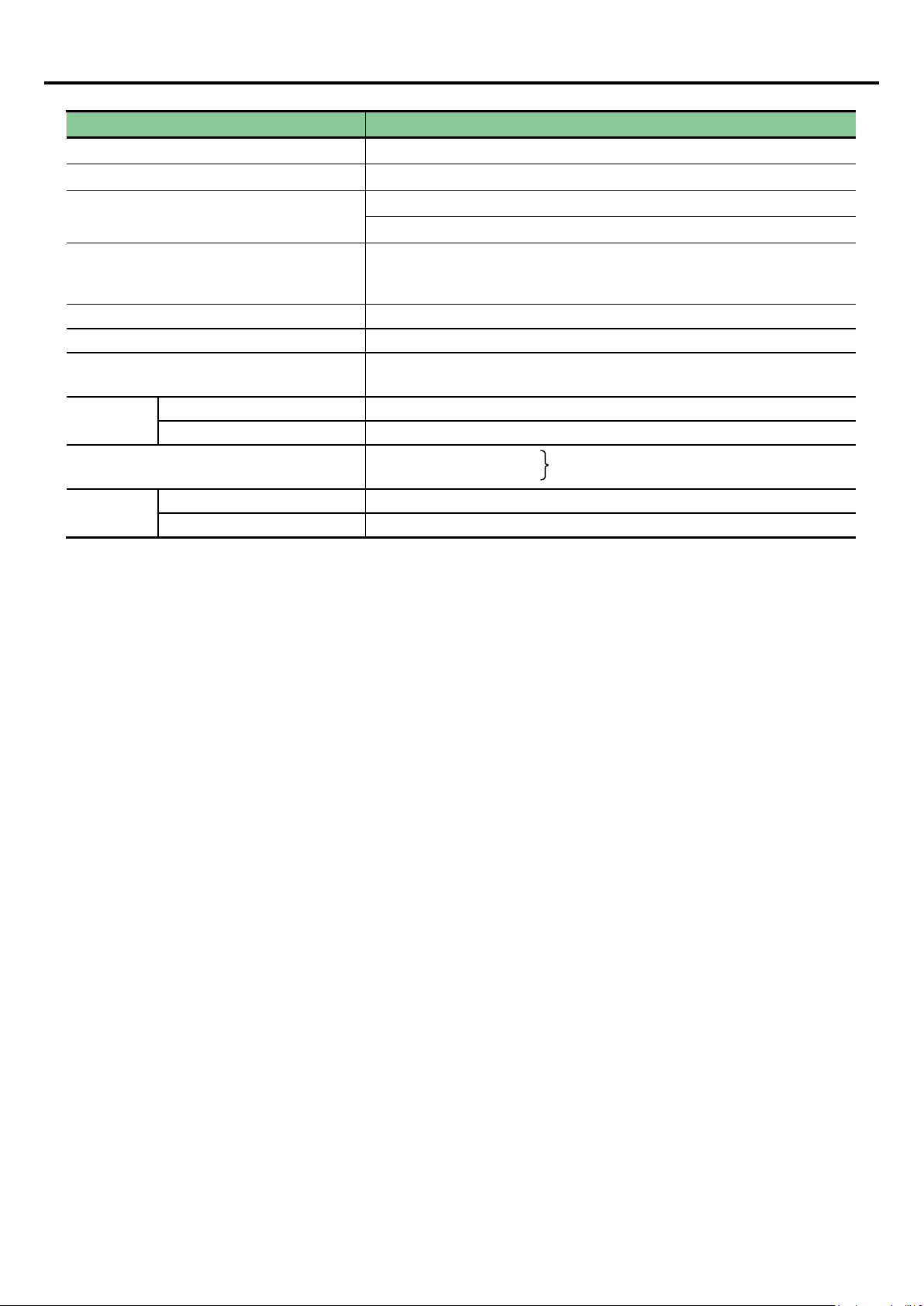
(1) System memory
%MW10.0 Resource operating status
%MW10.1 Resource switch / User ROM status
%MW10.2 Resource fatal fault factor
%MW10.3 Not used
%MW10.4 Resource nonfatal fault factor
%MW10.5 Not used
%MW10.6 CPU error factor
%MW10.7 Not used
%MW10.8, 9 Memory error factor
%MW10.10
%MW10.11
%MW10.12 Application error factor (fatal fault)
%MW10.13 Application error factor (nonfatal fault)
%MW10.14
|
%MW10.16
%MW10.17 Not used
%MW10.18
|
%MW10.20
%MW10.21 Not used
%MW10.22
|
%MW10.27
%MW10.28
|
%MW10.37
%MW10.38
|
%MW10.41
%MW10.42
%MW10.43
%MW10.44
|
%MW10.48
%MW10.49 Resource running information
%MW10.50, 51 Resource conguration/fault information
%MW10.52
|
%MW10.67
%MW10.68
|
%MW10.83
Not used
User fatal fault
factor 0 - factor 47
User nonfatal fault
factor 0 - factor 47
System denition error factor
Not used
Application program error factor
Announce relay
Not used
Conguration information
Conguration fault information
%MW10.84
|
%MW10.297
%MW10.298 User ROM status
%MW10.299 SPF original announce relay
%MW10.300
|
%MW10.511
Notes:
1) Be sure not to write any data to Not used areas.
2) Information of system ags in the system memory areas
can be referenced from application programs.
However, do not use it as “an event variable” for executing
event tasks in application programs.
(Some addresses are unavailable for starting tasks.)
Not used
Not used
1-11
Page 21

Section 1 Specications
(2) Resource operating status %MW10.0 (Read only)
This area indicates the resource (main unit) operating status and operating modes.
Address Name Description
%MX10.0.0 Run ON while the main unit is running.
%MX10.0.1 Stop ON while the main unit is stopped.
%MX10.0.2 Fatal fault ON when a fatal error occurs in the main unit.
%MX10.0.3 Nonfatal fault ON when a nonfatal error occurs in the main unit.
%MX10.0.4
|
%MX10.0.8
%MX10.0.9 Automatic operation mode ON while in the automatic operation mode.
%MX10.0.10 Not used
%MX10.0.11 Battery-less operation mode ON while in the battery-less operation mode.
%MX10.0.12
|
%MX10.0.15
Automatic operation mode
In this mode, the main unit starts operation when the power switch is turned ON. SPF is always set in this mode.
Not used
Not used
Battery-less operation mode
In this mode, all memories are initialized (assigned initial values or cleared to zero) when the power of the main unit is turned
ON. The battery voltage is not checked. You can enable or disable this mode in the “CPU running denition” on the “Main unit
parameter” dialog box.
(3) Resource switch / User ROM state %MW10.1 (Read only)
Address Name Description
%MX10.1.0
|
%MX10.1.5
%MX10.1.6 User ROM card connection state
%MX10.1.7 User ROM card write protect
%MX10.1.8 STOP position ON if the set bit is OFF (STOP) when using the remote RUN/STOP function
%MX10.1.9 Not used
%MX10.1.10 TERM position ON when the remote RUN/STOP function is not used
%MX10.1.11
|
%MX10.1.15
Not used
ON: Connected
OFF: Not connected
ON: Write-protected
OFF: Write-permitted (enabled when “%MX10.1.6” is ON)
Not used
1-12
Page 22
Section 1 Specications
(4) Resource fatal fault factor %MW10.2 (Read only)
This area indicates the factors of fatal faults. If a fatal fault occurs, the resource (main unit) stops operation.
Address Name Description
%MX10.2.0 CPU error ON when a fatal fault occurs in the main unit.
%MX10.2.1 Not used
%MX10.2.2 Memory error ON when an error occurs in the memory in the main unit.
%MX10.2.3 Not used
%MX10.2.4 Application error ON when an error is found in an application program or system denition.
%MX10.2.5 I/O error
%MX10.2.6
|
%MX10.2.12
%MX10.2.13 Other hardware error ON when an error occurs in hardware other than the CPU, memory and I/O.
%MX10.2.14 Not used
%MX10.2.15 User fatal fault
Not used
ON when communication between the main unit and a healthy unit is
interrupted. I/O errors are not detected if no healthy unit is mounted.
ON when one of the user fatal fault ags (%MX10.14.0 to %MX10.166.15) is
turned ON by an application program.
(5) Resource nonfatal fault factor %MW10.4 (Read only)
This area indicates the factors of nonfatal faults. Even if a nonfatal fault occurs, the resource (main unit) continues operation.
Address Name Description
%MX10.4.0
%MX10.4.1
%MX10.4.2 Memory error ON when an error occurs in the memory in the main unit.
%MX10.4.3 Not used
%MX10.4.4 Application error ON when an error is found in an application program or system denition.
%MX10.4.5
|
%MX10.4.13
%MX10.4.14 Battery error
Not used
Not used
ON when voltage of the data backup battery drops or when the battery
connection switch is OFF.
%MX10.4.15 User nonfatal fault
ON when one of the user nonfatal fault ags (%MX10.18.0 to %MX10.20.15)
is turned ON by a user program.
(6) CPU error factor %MW10.6 (Read only)
Address Name Description
%MX10.6.0 Arithmetic processor error Hardware error in the arithmetic LSI in the main unit
%MX10.6.1
|
%MX10.6.15
Not used
1-13
Page 23
Section 1 Specications
(7) Memory error factor %MW10.8, %MW10.9 (Read only)
Address Name Description Level
%MX10.8.0 System ROM error ON when an error occurs in the system ROM in the main unit. Fatal fault
%MX10.8.1 System RAM error ON when an error occurs in the system RAM in the main unit. Fatal fault
%MX10.8.2 Application ROM error
%MX10.8.3 Application RAM error
%MX10.8.4
|
%MX10.9.13
%MX10.9.14
%MX10.9.15 Memory backup error
Notes:
1) This bit is also set to “1” when an error occurs in the user ROM card.
<System operation after a memory error occurs>
If a memory backup error occurs, the entire user memory area is reset to 0 (zero). When any of the bits %MX10.8.0 to
%MX10.8.3 is set to ON, there is a possibility of a hardware fault. Therefore, even if the power is turned OFF and then ON
again, a fatal fault may recur due to a memory error.
Not used
Power down processing
error
ON when an error occurs in the ROM in the main unit for storing
application programs.
ON when an error occurs in the RAM in the main unit for storing
application programs.
ON when power down processing is not performed normally.
This bit can be set OFF by an application program.
ON when no power-failure-time data is retained.
This bit can be set OFF by an application program.
Fatal fault
(Note 1)
Fatal fault
Nonfatal fault
Nonfatal fault
(8) Application error factor %MW10.12, %MW10.13 (Read only)
Address Name Description Level
%MX10.12.0 System denition error ON when an error is found in the system denition. Fatal fault
%MX10.12.1 Application program error ON when an error is found in an application program. Fatal fault
%MX10.12.2
|
%MX10.12.15
%MX10.13.0 Not used
%MX10.13.1 Application program error ON when an error is found in an application program. Nonfatal fault
%MX10.13.2
|
%MX10.13.15
Not used
Not used
1-14
Page 24

Section 1 Specications
(9) User fatal fault %MW10.14 to %MW10.16
Address Name Description
%MX10.14.0 User fatal fault factor 0
| |
%MX10.14.15 User fatal fault factor 15
%MX10.15.0 User fatal fault factor 16
| |
%MX10.15.15 User fatal fault factor 31
%MX10.16.0 User fatal fault factor 32
| |
%MX10.16.15 User fatal fault factor 47
A fatal error occurs and the main unit stops when any of these bits is set to
ON by an application program.
(10) User nonfatal fault %MW10.18 to %MW10.20
Address Name Description
%MX10.18.0 User nonfatal fault factor 0
| |
%MX10.18.15 User nonfatal fault factor 15
%MX10.19.0 User nonfatal fault factor 16
| |
A nonfatal error occurs when any of these bits is set to ON by an application
program. The main unit continues operation.
Set to OFF the bit that has been set to ON by the application program to
restore the main unit from a nonfatal fault condition.
%MX10.19.15 User nonfatal fault factor 31
%MX10.20.0 User nonfatal fault factor 32
| |
%MX10.20.15 User nonfatal fault factor 47
1-15
Page 25

Section 1 Specications
(11) System denition error factor %MW10.22 to %MW10.27 (Read only)
Address Name Description Level
%MX10.22.0 Not used
%MX10.22.1 System denition error
%MX10.22.2
|
%MX10.22.9
%MX10.22.10 CPU running denition error ON when the system denition contains an error. Fatal fault
%MX10.22.11
%MX10.22.12
%MX10.22.13
%MX10.22.14 CPU running denition 3 error ON when the running denition of SPF contains an error. Fatal fault
%MX10.22.15 CPU running denition 2 error ON when the running denition of SPF contains an error. Fatal fault
%MX10.23.0
%MX10.23.1
%MX10.23.2
%MX10.23.3
%MX10.23.4
%MX10.23.5
|
%MX10.23.15
%MX10.24.0 Not used
Not used
CPU memory boundary
denition error
Not used
CPU I/O group denition error
for default tasks
CPU I/O group denition error
for level 0 tasks
CPU I/O group denition error
for level 1 tasks
CPU I/O group denition error
for level 2 tasks
CPU I/O group denition error
for level 3 tasks
Not used
ON when the contents of the system denition in the main unit do
not match the actual system conguration.
ON when the memory space used by an application program
exceeds the total memory capacity.
ON when an input unit is dened for an output unit. Fatal fault
Fatal fault
Fatal fault
%MX10.24.1
%MX10.24.2
|
%MX10.24.15
%MX10.27.0
%MX10.27.1
|
%MX10.27.15
Expansion unit running
denition error
Not used
Communication unit/board
running denition error
Not used
ON when the running denition of the expansion unit contains an
error.
ON when the running denition of the communication unit/board
contains an error.
Fatal fault
Fatal fault
1-16
Page 26

Section 1 Specications
(12) Application program error factor %MW10.38 to %MW10.41
Address Name Description Level
%MX10.38.0 Application WDT error
%MX10.38.1 Application execution error
%MX10.38.2
|
%MX10.38.10
%MX10.38.11 FB instance setup error ON when the specied storage address is not found. Fatal fault
%MX10.38.12 Initial value setup error
%MX10.38.13 SFM boundary denition error
%MX10.38.14 POU instruction error ON when there is an error in the POU. Fatal fault
%MX10.38.15 Task registration error ON when there is an error in the task registration. Fatal fault
%MX10.39.0 Missing level 0 task
%MX10.39.1 Missing level 1 task
%MX10.39.2 Missing level 2 task
%MX10.39.3 Missing level 3 task
%MX10.39.4 Level 0 task slow-down
%MX10.39.5 Level 1 task slow-down
%MX10.39.6 Level 2 task slow-down
Not used
ON when the execution time of a default task exceeds the
preset value of a watchdog timer.
ON when an error occurs during user program execution that
causes “temporary size-over.”
ON when the set initial value exceeds the dened range of a
storage area.
ON when the set size exceeds the capacity of the system FB
instance memory (SFM).
ON when a task is missing.
These bits can be set OFF by an application program.
ON when program execution is deferred and the predened
xed cycle time is not Maintained.
These bits can be set OFF by an application program.
Fatal fault
Fatal fault
Fatal fault
Fatal fault
Nonfatal fault
Nonfatal fault
%MX10.39.7 Level 3 task slow-down
%MX10.39.8
|
%MX10.40.3
%MX10.40.4 Missing level 4 task
%MX10.40.5 Missing level 10 task
%MX10.40.6 Missing level 11 task
%MX10.40.7 Missing level 12 task
%MX10.40.8 Missing level 13 task
%MX10.40.9 Missing level 14 task
%MX10.40.10 Missing level 15 task
%MX10.40.11 Missing level 16 task
%MX10.40.12 Missing level 17 task
%MX10.40.13 Missing level 18 task
%MX10.40.14 Missing level 19 task
%MX10.40.15 Not used
%MX10.41.0
|
%MX10.41.3
Not used
Not used
ON when a task is missing.
These bits can be set OFF by an application program.
Nonfatal fault
1-17
Page 27

Section 1 Specications
%MX10.41.4 Level 4 task slow-down
%MX10.41.5 Level 10 task slow-down
%MX10.41.6 Level 11 task slow-down
%MX10.41.7 Level 12 task slow-down
%MX10.41.8 Level 13 task slow-down
%MX10.41.9 Level 14 task slow-down
%MX10.41.10 Level 15 task slow-down
%MX10.41.11 Level 16 task slow-down
%MX10.41.12 Level 17 task slow-down
%MX10.41.13 Level 18 task slow-down
%MX10.41.14 Level 19 task slow-down
%MX10.41.15 Not used
ON when program execution is deferred and the predened
xed cycle time is not Maintained.
These bits can be set OFF by an application program.
(13) Announce relay %MW10.42, %MW10.43 (Read only)
Address Name Description
%MX10.42.0 Initial ag
ON at the rst startup after program download and at initial startup (cold start).
This bit is not set to OFF during operation.
Nonfatal fault
%MX10.42.1 Power-off ag ON when a power-off condition occurred in the preceding session.
%MX10.42.2
|
%MX10.42.15
%MX10.43.0 Level 0 start ag ON during the rst execution of level 0 task.
%MX10.43.1 Level 1 start ag ON during the rst execution of level 1 task.
%MX10.43.2 Level 2 start ag ON during the rst execution of level 2 task.
%MX10.43.3 Level 3 start ag ON during the rst execution of level 3 task.
%MX10.43.4 Level 4 start ag ON during the rst execution of level 4 task.
%MX10.43.5 Level 10 start ag ON during the rst execution of level 10 task.
%MX10.43.6 Level 11 start ag ON during the rst execution of level 11 task.
%MX10.43.7 Level 12 start ag ON during the rst execution of level 12 task.
%MX10.43.8 Level 13 start ag ON during the rst execution of level 13 task.
%MX10.43.9 Level 14 start ag ON during the rst execution of level 14 task.
%MX10.43.10 Level 15 start ag ON during the rst execution of level 15 task.
%MX10.43.11 Level 16 start ag ON during the rst execution of level 16 task.
%MX10.43.12 Level 17 start ag ON during the rst execution of level 17 task.
%MX10.43.13 Level 18 start ag ON during the rst execution of level 18 task.
Not used
%MX10.43.14 Level 19 start ag ON during the rst execution of level 19 task.
%MX10.43.15 Default task start ag ON during the rst execution of the default task.
1-18
Page 28

Section 1 Specications
(14) Resource running information %MW10.49 (Read only)
Address Name Description
%MX10.49.0 Main unit running ON while the main unit is running.
%MX10.49.1
|
%MX10.49.15
(15) Resource conguration/fault information %MW10.50, %MW10.51 (Read only)
The resource conguration/fault information enables an application program to recognize the status of the main unit.
Not used
Resource conguration
information
OFF OFF Nonexistent
ON OFF Normal (running or stopped)
ON ON Nonfatal fault (running or stopped)
OFF ON Fatal fault
Address Name Description
%MX10.50.0 Main unit conguration ON while the main unit is running normally or in a nonfatal fault condition.
%MX10.50.1
|
%MX10.50.15
%MX10.51.0 Main unit error
%MX10.51.1
|
%MX10.51.15
Not used
Not used
Resource fault
information
Resource status
ON while the main unit is stopped due to a fatal fault or running in a nonfatal
fault condition.
1-19
Page 29

Section 1 Specications
(16) Conguration/conguration fault information %WM10.52 to %WM10.83 (Read only)
This area indicates the status of the expansion units/boards.
Address Name Description
%MX10.52.0 Main unit conguration ON when the main unit is in a normal or a nonfatal fault condition.
%MX10.52.1 Expansion right side unit 1 conguration
%MX10.52.2 Expansion right side unit 2 conguration
%MX10.52.3 Expansion right side unit 3 conguration
%MX10.52.4 Expansion right side unit 4 conguration
%MX10.52.5 Expansion right side unit 5 conguration
%MX10.52.6 Expansion right side unit 6 conguration
%MX10.52.7 Expansion right side unit 7 conguration
%MX10.52.8
|
%MX10.58.3
%MX10.58.4 Front board conguration ON when the front board is in a normal or nonfatal fault condition.
%MX10.58.5
|
%MX10.64.7
%MX10.64.8 Expansion left side unit conguration
%MX10.64.9
|
%MX10.67.15
%MX10.68.0 Main unit error ON when the main unit is in a nonfatal or fatal fault condition.
Not used
Not used
Not used
When the main unit is powered on, the bit corresponding to the
connected expansion right side unit (including a healthy unit) is set
ON.
If an expansion right side unit is dropped while the main unit is
running, only the conguration bit of the healthy unit is set OFF.
The other conguration bits reMain ON.
* “Expansion right side unit 7 conguration” is assigned only to a
healthy unit when six expansion units (max.) are connected.
ON when the expansion left side unit is in a normal or nonfatal fault
condition.
%MX10.68.1 Expansion right side unit 1 error
%MX10.68.2 Expansion right side unit 2 error
%MX10.68.3 Expansion right side unit 3 error
%MX10.68.4 Expansion right side unit 4 error
%MX10.68.5 Expansion right side unit 5 error
%MX10.68.6 Expansion right side unit 6 error
%MX10.68.7 Expansion right side unit 7 error
%MX10.68.8
|
%MX10.74.3
%MX10.74.4 Front board error
%MX10.74.5
|
%MX10.80.7
%MX10.80.8 Expansion left side unit error
%MX10.80.9
|
%MX10.83.15
Not used
Not used
When a healthy unit is mounted and an expansion right side unit is
dropped, only the error bit corresponding to the healthy unit is set
ON. The other error bits of expansion right side units reMain OFF.
* “Expansion right side unit 7 error” is assigned only to a healthy
unit when six expansion units (max.) are connected.
ON when the front board is in a nonfatal or fatal fault condition.
(Note 1)
ON when the expansion left side unit is in a nonfatal or fatal fault
condition. (Note 1)
Notes:
1) A dropout of communication boards/units is not detected.
However, during the CPU link communication, a nonfatal fault occurs if a link station is dropped.
1-20
Page 30

Section 1 Specications
(17) User ROM status %MW10.298 (Read only)
This area indicates the status of the ROM in the SPF main unit.
Address Name Description
ON when a mismatch occurs between the contents of the RAM and
%MX10.298.0 Built-in ash memory mismatch
%MX10.298.1 User ROM card mismatch
%MX10.298.2
|
%MX10.298.15
Not used
(18) SPF original announce relay %MW10.299 (Read only)
Address Name Description
those of the built-in ash memory in the main unit.
* Transferring data from the RAM to the built-in ash memory sets this
bit to OFF.
ON when a mismatch occurs between the contents of the RAM in the
main unit and those of the mounted user ROM card (ash memory).
* Transferring data from the RAM to the user ROM card sets this bit to
OFF.
%MX10.299.0 Enable constant scanning ON while the constant scanning function is used.
%MX10.299.1 Enable remote RUN/STOP function ON while the remote RUN/STOP function is used.
%MX10.299.2 Enable I/O status latch function ON while the I/O status latch function is used.
%MX10.299.3
|
%MX10.299.15
Not used
1-21
Page 31

Section 1 Specications
1-3-8 SPF original special relay/register area
*Attribute (R: read only, R/W: readable and writable)
(1) Built-in calendar data %MW1.61442 to %MW1.61449
Address Name Description Attribute
Sets the year data (last two digits of Christian year) of the built-in
%MW1.61442 Year data
%MW1.61443 Month data Sets the month data of the built-in calendar. (BCD: 01 to 12)
%MW1.61444 Day data Sets the day data of the built-in calendar. (BCD: 01 to 31)
%MW1.61445 Hour data Sets the hour data of the built-in calendar. (BCD: 00 to 23)
%MW1.61446 Minute data Sets the minute data of the built-in calendar. (BCD: 00 to 59)
%MW1.61447 Second data Sets the second data of the built-in calendar. (BCD: 00 to 59)
calendar. (BCD: 00 to 99)
Example: 17 for 2017
R
(W)
*1
%MW1.61448 Day of the week data
Address Name Description Attribute
%MX1.61449.0 Calendar write request
%MX1.61449.1
|
%MX1.61449.15
*1 Only when the “calendar write request” is ON, writing can be performed.
Not used
Sets the day of the week data of the built-in calendar.
0: Sun, 1: Mon, 2: Tue, 3: Wed, 4: Thu, 5: Fri, 6: Sat
When this ag is set ON, “year, month, day, time, minute, and second
data” set in the “built-in calendar data (%MW1.61442 to %MW1.61447)”
are written to the built-in calendar.
This bit is automatically set OFF.
R
R/W
(2) Battery information %MW1.61450
Address Name Description Attribute
Stores the A/D conversion value of battery voltage of the battery (primary
battery) built in the main unit.
Battery voltage = Battery voltage A/D conversion value * 4.883 [mV]
R
%MW1.61450
Battery voltage A/D
conversion value
(3) Pulse catch input %MW1.61472 to %MW1.61479
These are special relays for the pulse catch input function of the main unit.
Address Name Description Attribute
%MX1.61472.0 Pulse catch rising edge 0
| |
%MX1.61472.15 Pulse catch rising edge 15
%MX1.61473.0 Pulse catch rising edge 16
| |
%MX1.61473.15 Pulse catch rising edge 31
%MX1.61474.0 Pulse catch rising edge 32
| |
%MX1.61474.3 Pulse catch rising edge 35
%MX1.61474.4
|
%MX1.61475.15
Not used
ON for one scan period during the next scan when a rising edge
pulse that is inputted to the input terminals X0 to X35 of the main
unit is detected.
R
1-22
Page 32

Section 1 Specications
%MX1.61476.0 Pulse catch falling edge 0
| |
%MX1.61476.15 Pulse catch falling edge 15
%MX1.61477.0 Pulse catch falling edge 16
| |
%MX1.61477.15 Pulse catch falling edge 31
%MX1.61478.0 Pulse catch falling edge 32
| |
%MX1.61478.3 Pulse catch falling edge 35
%MX1.61478.4
|
%MX1.61479.15
Not used
ON for one scan period during the next scan when a falling edge
pulse that is inputted to the input terminals X0 to X35 of the main
unit is detected.
R
(4) Memories related to interrupt %MW1.61480 to %MW1.61498
These are special relays for the external interrupt input function of the main unit.
1) Interrupt event ag %MW1.61480 to %MW1.61491
Address Name Description Attribute
%MX1.61480.0
| |
%MX1.61480.15
%MX1.61481.0
|
%MX1.61482.15
%MX1.61483.0
| |
%MX1.61483.15
%MX1.61484.0
|
%MX1.61485.15
%MX1.61486.0
| |
%MX1.61486.15
%MX1.61487.0
|
%MX1.61488.15
%MX1.61489.0
| |
%MX1.61489.7
%MX1.61489.8
|
%MX1.61491.15
Interrupt input event ag for
rising edge 0
Interrupt input event ag for
rising edge 15
Not used
Interrupt input event ag for
falling edge 0
Interrupt input event ag for
falling edge 15
Not used
Interrupt input event ag for
rising and falling edges 0
Interrupt input event ag for
rising and falling edges 15
Not used
High-speed counter match ag
CH0
High-speed counter match ag
CH7
Not used
This ag is a special event address that is used for the event
address to set conditions for an event task and not set to ON in
practice. When a rising edge of the signal of the input terminals
X0 to X15 in the main unit is detected, the set event task
operates.
This ag is a special event address that is used for the event
address to set conditions for an event task and not set to ON in
practice. When a falling edge of the signal of the input terminals
X0 to X15 in the main unit is detected, the set event task
operates.
This ag is a special event address that is used for the event
address to set conditions for an event task and not set to ON in
practice. When a rising or falling edge of the signal of the input
terminals X0 to X15 in the main unit is detected, the set event
task operates.
This ag is a special event address that is used for the event
address to set conditions for an event task and not set to ON
in practice. When the current value coincides with the set high-
speed counter value, the set event task operates.
–
–
–
–
1-23
Page 33

Section 1 Specications
2) External interrupt factor occurrence %MW1.61492 to %MW1.61497
Address Name Description Attribute
%MX1.61492.0
| |
%MX1.61492.15
%MX1.61493.0
|
%MX1.61494.15
%MX1.61495.0
| |
%MX1.61495.15
%MX1.61496.0
|
%MX1.61497.15
3) Interrupt mask status ag %MW1.61498
Address Name Description Attribute
%MX1.61498.0
External interrupt factor
occurrence for rising edge 0
External interrupt factor
occurrence for rising edge 15
Not used
External interrupt factor
occurrence for falling edge 0
External interrupt factor
occurrence for falling edge 15
Not used
Interrupt mask status ag for
level 0 task
ON when an interrupt factor occurs due to detection of a rising
edge of the signal of the input terminals X0 to X15 in the main
unit. This memory can be read and reset (written) from an
application.
ON when an interrupt factor occurs due to detection of a falling
edge of the signal of the input terminals X0 to X15 in the main
unit. This memory can be read and reset (written) from an
application.
ON when interrupt is disabled in the level 0 task.
R/W
R/W
%MX1.61498.1
%MX1.61498.2
%MX1.61498.3
%MX1.61498.4
%MX1.61498.5
|
%MX1.61498.9
%MX1.61498.10
%MX1.61498.11
|
%MX1.61498.15
Interrupt mask status ag for
level 1 task
Interrupt mask status ag for
level 2 task
Interrupt mask status ag for
level 3 task
Interrupt mask status ag for
level 4 task
Not used
Interrupt mask status ag for
level 10 to 19 tasks
Not used
ON when interrupt is disabled in the level 1 task.
ON when interrupt is disabled in the level 2 task.
ON when interrupt is disabled in the level 3 task.
ON when interrupt is disabled in the level 4 task.
ON when interrupt is disabled in the level 10 to 19 tasks.
R
R
1-24
Page 34

Section 1 Specications
(5) Memories related to high-speed counter %WM1.61536 to %WM1.61561, %WM3.61536 to %WM3.61577
These are special relays/registers for the high-speed counter function built in the main unit.
1) High-speed counter control ag %MW1.61536 to %MW1.61538
Address Name Description Attribute
%MX1.61536.0
| |
%MX1.61536.7
%MX1.61536.8
|
%MX1.61536.15
%MX1.61537.0
| |
%MX1.61537.7
%MX1.61537.8
|
%MX1.61537.15
%MX1.61538.0
| |
%MX1.61538.7
%MX1.61538.8
|
%MX1.61538.15
High-speed counter CH0
count enable/disable
High-speed counter CH7
count enable/disable
Not used
High-speed counter CH0
current value clear
High-speed counter CH7
current value clear
Not used
High-speed counter CH0
latch status
High-speed counter CH7
latch status
Not used
Sets the counting operation of the high-speed counter.
ON: Disable counting, OFF: Enable counting
* This setting is reected at the end of the scan.
Clears the counter current value of the high-speed counter.
ON: Clear, OFF: Clear release
* Operation is performed at the end of the scan.
ON when the latch status is ON at the end of the scan or at the
execution of the high-speed counter current value latch instruction
(R_HSC_LATCH).
* Set to OFF this memory by an application.
R/W
R/W
R/W
2) High-speed counter current value latch data %MD1.61546 to %MD1.61560
Address Name Description Attribute
%MD1.61546
| |
%MD1.61560
High-speed counter CH0
current value latch data
High-speed counter CH7
current value latch data
Stores the latch data of the high-speed counter current value.
* Updated at the end of the scan or at the execution of the high-
speed counter current value latch instruction (R_HSC_LATCH).
R
1-25
Page 35

Section 1 Specications
3) High-speed counter direction signal %MW3.61536
Address Name Description Attribute
%MX3.61536.0
| |
%MX3.61536.7
%MX3.61536.8
|
%MX3.61536.15
4) High-speed counter current value register / set value register %MD3.61546 to %MD3.61576
Address Name Description Attribute
%MD3.61546
%MD3.61560
%MD3.61562
| |
%MD3.61576
High-speed counter CH0
direction signal (by software)
High-speed counter CH7
direction signal (by software)
Not used
High-speed counter CH0
current value
High-speed counter CH7
current value
High-speed counter CH0
set value
High-speed counter CH7
set value
Sets the direction signal (by software) of the high-speed counter.
OFF: Forward, OFF: Reverse
* This setting is reected at the end of the scan or at the execution
of the high-speed counter ag control instruction
(W_HSC_FLG).
Stores the current value of the high-speed counter.
* Updated at the end of the scan or at the execution of the high-
speed counter current value direct read instruction (R_READ)
or high-speed counter current/set value write instruction
(W_HSC).
Stores the set value of the high-speed counter.
* Updated at the execution of the high-speed counter current/set
value write instruction (W_HSC).
R/W
R | |
R
1-26
Page 36

Section 1 Specications
(6) Memories related to pulse/positioning %MW1.61600 to %MW1.61769, %MW3.61600 to %MW3.61613
These are special relays/registers for pulse output and positioning functions built in the main unit.
1) Pulse control ag %MW1.31600 to %MW1.61601
Address Name Description Attribute
Sets the pulse output start timing.
%MX1.61600.0 Pulse output start timing
%MX1.61600.1
|
%MX1.61600.15
%MX1.61601.0 Pulse output status display CH0
Not used
OFF: At the execution of the pulse output instruction.
ON: At the end of the scan
Displays the status of the pulse output CH0.
ON: Ready for pulse output, OFF: Pulse outputting
R/W
%MX1.61601.1 Pulse output status display CH1
%MX1.61601.2 Pulse output status display CH2
%MX1.61601.3 Pulse output status display CH3
%MX1.61601.4
|
%MX1.61601.15
Not used
Displays the status of the pulse output CH1.
ON: Ready for pulse output, OFF: Pulse outputting
R
Displays the status of the pulse output CH2.
ON: Ready for pulse output, OFF: Pulse outputting
Displays the status of the pulse output CH3.
ON: Ready for pulse output, OFF: Pulse outputting
1-27
Page 37

Section 1 Specications
2) Positioning parameter display %MW1.61610 to %MW1.61769
Address Name Description Attribute
%MW1.61610
%MW1.61611 [H]
%MW1.61612 Startup frequency (0 to 200,000 Hz) [L]
%MW1.61613 [H]
%MW1.61614 Stop speed (0 to 200,000 Hz) [L]
%MW1.61615 [H]
%MW1.61616 Acceleration time (1 to 30,000 ms) [L]
%MW1.61617 [H]
%MW1.61618 Deceleration time (1 to 30,000 ms) [L]
%MW1.61619 [H]
%MW1.61620
%MW1.61621
%MW1.61622 Creep speed (for origin return) (0 to 200,000 Hz) [L]
%MW1.61623 [H]
%MW1.61624 LS address (for origin return) (0 to 15) [L]
%MW1.61625 Z-phase signal address (for origin return) (0 to 15) [H]
%MW1.61626
%MW1.61627
%MW1.61628
%MW1.61629 [H]
%MW1.61630
|
%MW1.61649
%MW1.61650
%MW1.61651 [H]
%MW1.61652 Startup frequency (0 to 200,000 Hz) [L]
%MW1.61653 [H]
%MW1.61654 Stop speed (0 to 200,000 Hz) [L]
%MW1.61655 [H]
%MW1.61656 Acceleration time (1 to 30,000 ms) [L]
%MW1.61657 [H]
%MW1.61658 Deceleration time (1 to 30,000 ms) [L]
%MW1.61659 [H]
%MW1.61660
%MW1.61661
%MW1.61662 Creep speed (for origin return) (0 to 200,000 Hz) [L]
%MW1.61663 [H]
%MW1.61664 LS address (for origin return) (0 to 15) [L]
%MW1.61665 Z-phase signal address (for origin return) (0 to 15) [H]
%MW1.61666
%MW1.61667
%MW1.61668
%MW1.61669 [H]
%MW1.61670
|
%MW1.61689
Positioning parameter current
value for CH0
Positioning parameter current
value for CH1
Maximum frequency (1 to 200,000 Hz) [L]
Not used
Not used
Acceleration/deceleration time (for multi-axis control)
(1 to 30,000 ms)
Not used
Maximum frequency (1 to 200,000 Hz) [L]
Not used
Not used
Acceleration/deceleration time (for multi-axis control)
(1 to 30,000 ms)
Not used
[L]
[L]
R
R
R
R
R
R
1-28
Page 38

Section 1 Specications
Address Name Description Attribute
%MW1.61690
%MW1.61691 [H]
%MW1.61692 Startup frequency (0 to 200,000 Hz) [L]
%MW1.61693 [H]
%MW1.61694 Stop speed (0 to 200,000 Hz) [L]
%MW1.61695 [H]
%MW1.61696 Acceleration time (1 to 30,000 ms) [L]
%MW1.61697 [H]
%MW1.61698 Deceleration time (1 to 30,000 ms) [L]
%MW1.61699 [H]
%MW1.61700
%MW1.61701
%MW1.61702 Creep speed (for origin return) (0 to 200,000 Hz) [L]
%MW1.61703 [H]
%MW1.61704 LS address (for origin return) (0 to 15) [L]
%MW1.61705 Z-phase signal address (for origin return) (0 to 15) [H]
%MW1.61706
%MW1.61707
%MW1.61708
%MW1.61709 [H]
%MW1.61710
|
%MW1.61729
%MW1.61730
%MW1.61731 [H]
%MW1.61732 Startup frequency (0 to 200,000 Hz) [L]
%MW1.61733 [H]
%MW1.61734 Stop speed (0 to 200,000 Hz) [L]
%MW1.61735 [H]
%MW1.61736 Acceleration time (1 to 30,000 ms) [L]
%MW1.61737 [H]
%MW1.61738 Deceleration time (1 to 30,000 ms) [L]
%MW1.61739 [H]
%MW1.61740
%MW1.61741
%MW1.61742 Creep speed (for origin return) (0 to 200,000 Hz) [L]
%MW1.61743 [H]
%MW1.61744 LS address (for origin return) (0 to 15) [L]
%MW1.61745 Phase-Z signal address (for origin return) (0 to 15) [H]
%MW1.61746
%MW1.61747
%MW1.61748
%MW1.61749 [H]
%MW1.61750
|
%MW1.61769
Positioning parameter current
value for CH2
Positioning parameter current
value for CH3
Maximum frequency (1 to 200,000 Hz) [L]
Not used
Not used
Acceleration/deceleration time (for multi-axis control)
(1 to 30,000 ms)
Not used
Maximum frequency (1 to 200,000 Hz) [L]
Not used
Not used
Acceleration/deceleration time (for multi-axis control)
(1 to 30,000 ms)
Not used
[L]
[L]
R
R
R
R
R
R
1-29
Page 39

Section 1 Specications
3) Positioning current value display %MW3.61600 to %MW3.61609
Address Name Description Attribute
%MW3.61600
%MW3.61601 [H]
%MW3.61602 CH1 pulse output current value [L]
%MW3.61603 [H]
%MW3.61604 CH2 pulse output current value [L]
%MW3.61605 [H]
%MW3.61606 CH3 pulse output current value [L]
%MW3.61607 [H]
%MW3.61608
%MW3.61609
Notes:
1) The current value is updated at the execution of the pulse output HW register read instruction (PLS_R_CNT) and at the end
of the scan.
4) Positioning step position %MW3.61610 to %MW3.61613
Positioning current value
(Note 1)
Not used
CH0 pulse output current value [L]
R
Address Name Description Attribute
%MW3.61610
%MW3.61611 Step position for CH1
%MW3.61612 Step position for CH2 * When using Gr 1 for multi-axis.
%MW3.61613 Step position for CH3
Notes:
2) The positioning step position can be rewritten only when the positioning instruction is not executed.
Positioning step position
(Note 2)
Step position for CH0 * When using Gr 0, 2, and 3 for multi-axis.
R/W
1-30
Page 40

Section 1 Specications
(7) Memories related to general purpose communication %MW1.61793 to %MW1.61838
These are special relays/registers for the general purpose communication function of the communication unit/board.
Address Name Description Attribute
%MX1.61793.0
%MX1.61793.1 Displays the CTS status of PORT 1.
%MX1.61793.2 Xon/Xoff status (PORT 1)
%MX1.61793.3
|
%MX1.61793.15
%MX1.61794.0
%MX1.61794.1 Displays the CTS status of PORT 2.
%MX1.61794.2 Xon/Xoff status (PORT 2)
%MX1.61794.3
|
%MX1.61795.1
%MX1.61795.2 Xon/Xoff status (PORT 3)
%MX1.61795.3
|
%MX1.61796.1
%MX1.61796.2 Xon/Xoff status (PORT 4)
%MX1.61796.3
|
%MX1.61796.15
Control signal status (PORT 1)
Not used
Control signal status (PORT 2)
Not used
Not used
Not used
Displays the RTS status of PORT 1.
Displays the reception status of Xon/Xoff of PORT 1.
This ag is set ON when Xoff is received and OFF when Xon is
received.
Displays the RTS status of PORT 2.
Displays the reception status of Xon/Xoff of PORT 2.
This ag is set ON when Xoff is received and OFF when Xon is
received.
Displays the reception status of Xon/Xoff of PORT 3.
This ag is set ON when Xoff is received and OFF when Xon is
received.
Displays the reception status of Xon/Xoff of the PORT 4.
This ag is set ON when Xoff is received and OFF when Xon is
received.
R
R
R
R
Address Name Description
%MW1.61798 Mode status (PORT 1)
%MW1.61799 Mode status (PORT 2)
%MW1.61800 Mode status (PORT 3)
%MW1.61801 Mode status (PORT 4)
%MW1.61802
|
%MW1.61810
Not used
Displays the setting status of the communication mode.
0000H: Loader communication
0011H: General-purpose communication
0020H: CPU link communication (SPF mode)
1-31
R
Page 41

Section 1 Specications
Address Name Description Attribute
%MW1.61811
%MW1.61812
%MW1.61813
%MW1.61814
%MW1.61815
|
%MW1.61818
%MW1.61819
%MW1.61820
%MW1.61821
%MW1.61822
%MW1.61823
|
%MW1.61826
%MW1.61827
Parity error counter
(PORT 1)
Framing error counter
(PORT 1)
Overrun counter
(PORT 1)
Receive buffer overow
counter (PORT 1)
Not used
Parity error counter
(PORT 2)
Framing error counter
(PORT 2)
Overrun counter
(PORT 2)
Receive buffer overow
counter (PORT 2)
Not used
Parity error counter
(PORT 3)
Counted up when a parity error occurs during data reception.
Reset to 0 and restarted when the maximum value (FFFF) is exceed.
Counted up when a framing error occurs during data reception.
Reset to 0 and restarted when the maximum value (FFFF) is exceed.
R/W
Counted up when an overrun occurs during data reception.
Reset to 0 and restarted when the maximum value (FFFF) is exceed.
Counted up when a receive buffer overow occurs during data reception.
Reset to 1 and restarted when the maximum value (FFFF) is exceed.
Counted up when a parity error occurs during data reception.
Reset to 0 and restarted when the maximum value (FFFF) is exceed.
%MW1.61828
%MW1.61829
%MW1.61830
%MW1.61831
|
%MW1.61834
%MW1.61835
%MW1.61836
%MW1.61837
%MW1.61838
Framing error counter
(PORT 3)
Overrun counter
(PORT 3)
Receive buffer overow
counter (PORT 3)
Not used
Parity error counter
(PORT 4)
Framing error counter
(PORT 4)
Overrun counter
(PORT 4)
Receive buffer overow
counter (PORT 4)
Counted up when a framing error occurs during data reception.
Reset to 0 and restarted when the maximum value (FFFF) is exceed.
R/W
Counted up when an overrun occurs during data reception.
Reset to 0 and restarted when the maximum value (FFFF) is exceed.
Counted up when a receive buffer overow occurs during data reception.
Reset to 1 and restarted when the maximum value (FFFF) is exceed.
Counted up when a parity error occurs during data reception.
Reset to 0 and restarted when the maximum value (FFFF) is exceed.
Counted up when a framing error occurs during data reception.
Reset to 0 and restarted when the maximum value (FFFF) is exceed.
R/W
Counted up when an overrun occurs during data reception.
Reset to 0 and restarted when the maximum value (FFFF) is exceed.
Counted up when a receive buffer overow occurs during data reception.
Reset to 1 and restarted when the maximum value (FFFF) is exceed.
1-32
Page 42

Section 1 Specications
(8) Memories related to CPU link %MW1.61858 to %MW1.62399
These are special relays/registers for the CPU link function of the communication unit/board.
Address Name Description Attribute
%MW1.61858
%MW1.61859 Not used
%MW1.61860 Link station error relay
%MW1.61861 Not used
%MW1.61862 PLC run relay
%MW1.61863 Not used
%MW1.61864 PLC error relay
%MW1.61865 Not used
%MW1.61866
Link station conguration
relay
Conguration data
(Station Nos. 0 and 1)
The bit Nos. 0 to F correspond to the station Nos. 0 to F respectively.
ON: When connected to the link (during communication)
OFF: When not connected to the link
The bit Nos. 0 to F correspond to the station Nos. 0 to F respectively.
ON: When disconnected from the link or when not connected to the link
although registered in the system denition
OFF: When connected to the link or not registered in the system
denition.
The bit Nos. 0 to F correspond to the station Nos. 0 to F respectively.
ON: When the “link station conguration relay” is ON and the station is
running.
OFF: In cases other than above
The bit Nos. 0 to F correspond to the station Nos. 0 to F respectively.
ON: When the “link station conguration relay” is ON and the station is
in a fatal or nonfatal fault condition.
OFF: In cases other than above
The upper 8 bits indicate the conguration data of the station No. 1.
The lower 8 bits indicate the conguration data of the station No. 0.
R
R
R
R
%MW1.61867
%MW1.61868
%MW1.61869
%MW1.61870
%MW1.61871
%MW1.61872
%MW1.61873
%MW1.61874
|
%MW1.61883
%MW1.61884 BCC error counter
%MW1.61885 No response counter
Conguration data
(Station Nos. 2 and 3)
Conguration data
(Station Nos. 4 and 5)
Conguration data
(Station Nos. 6 and 7)
Conguration data
(Station Nos. 8 and 9)
Conguration data
(Station Nos. A and B)
Conguration data
(Station Nos. C and D)
Conguration data
(Station Nos. E and F)
Not used
The upper 8 bits indicate the conguration data of the station No. 3.
The lower 8 bits indicate the conguration data of the station No. 2.
The upper 8 bits indicate the conguration data of the station No. 5.
The lower 8 bits indicate the conguration data of the station No. 4.
The upper 8 bits indicate the conguration data of the station No. 7.
The lower 8 bits indicate the conguration data of the station No. 6.
The upper 8 bits indicate the conguration data of the station No. 9.
The lower 8 bits indicate the conguration data of the station No. 8.
The upper 8 bits indicate the conguration data of the station No. B.
The lower 8 bits indicate the conguration data of the station No. A.
The upper 8 bits indicate the conguration data of the station No. D.
The lower 8 bits indicate the conguration data of the station No. C.
The upper 8 bits indicate the conguration data of the station No. F.
The lower 8 bits indicate the conguration data of the station No. E.
Counted up when a BCC error occurs during data reception.
Reset to 0 and restarted when the maximum value (FFFF) is exceed.
Counted up when no response occurs during data communication.
Reset to 0 and restarted when the maximum value (FFFF) is exceed.
R
R
%MW1.61886 Status data 1 Displays the initialization status of CPU link.
%MW1.61887 Not used
1-33
Page 43

Section 1 Specications
%MW1.61888
|
%MW1.61919
%MW1.61920
|
%MW1.61951
%MW1.61952
|
%MW1.61983
%MW1.61984
|
%MW1.62015
%MW1.62016
|
%MW1.62047
%MW1.62048
|
%MW1.62079
%MW1.62080
|
%MW1.62111
%MW1.62112
|
%MW1.62143
%MW1.62144
|
%MW1.62175
%MW1.62176
|
%MW1.62207
%MW1.62208
|
%MW1.62239
%MW1.62240
|
%MW1.62271
% M W 1 . 6 2 2 7 2
|
%MW1.62303
%MW1.62304
|
%MW1.62335
%MW1.62336
|
%MW1.62367
%MW1.62368
|
%MW1.62399
Station No. 0 Send area
Station No. 1 Send area
Station No. 2 Send area
Station No. 3 Send area
Station No. 4 Send area
Station No. 5 Send area
Station No. 6 Send area
Station No. 7 Send area
Station No. 8 Send area
Station No. 9 Send area
Station No. A Send area
Station No. B Send area
Station No. C Send area
Station No. D Send area
Station No. E Send area
Station No. F Send area
Send area of station No. 0
(reception area when viewed from other stations) [32 words]
Send area of station No. 1
(reception area when viewed from other stations) [32 words]
Send area of station No. 2
(reception area when viewed from other stations) [32 words]
Send area of station No. 3
(reception area when viewed from other stations) [32 words]
Send area of station No. 4
(reception area when viewed from other stations) [32 words]
Send area of station No. 5
(reception area when viewed from other stations) [32 words]
Send area of station No. 6
(reception area when viewed from other stations) [32 words]
Send area of station No. 7
(reception area when viewed from other stations) [32 words]
Send area of station No. 8
(reception area when viewed from other stations) [32 words]
Send area of station No. 9
(reception area when viewed from other stations) [32 words]
Send area of station No. A
(reception area when viewed from other stations) [32 words]
Send area of station No. B
(reception area when viewed from other stations) [32 words]
Send area of station No. C
(reception area when viewed from other stations) [32 words]
Send area of station No. D
(reception area when viewed from other stations) [32 words]
Send area of station No. E
(reception area when viewed from other stations) [32 words]
Send area of station No. F
(reception area when viewed from other stations) [32 words]
R
(W)
*1
*1 Only the send area of the self station can be written.
1-34
Page 44

Section 1 Specications
(9) Memories related to Ethernet %MW1.62400 to %MW1.62463, %MW3.62400 to %MW3.62463
These are special registers related to the Ethernet front board and expansion left side unit.
1) Special register non-retain area (for front board)
Address Name Description Attribute
%MW1.62400 MAC address (L)
Indicates the MAC address of the self station. R%MW1.62401 MAC address (M)
%MW1.62402 MAC address (H)
%MW1.62403 Not used
%MW1.62404 IP address (L)
%MW1.62405 IP address (H)
%MW1.62406 Subnet mask (L)
%MW1.62407 Subnet mask (H)
%MW1.62408 Default gateway address (L)
%MW1.62409 Default gateway address (H)
%MW1.62410
%MW1.62411 Not used
%MW1.62412
%MW1.62413 Not used
%MW1.62414 Sending retry number of times
%MW1.62415
%MW1.62416
%MW1.62417 Not used
TCP sending and receiving
timeout value
Loader command watch timer
value
Close process during TCP
sending timeout
Close process during
response receiving timeout
Indicates the IP address of the self station. R
Indicates the subnet mask R
Indicates the IP address of the default gateway R
Indicates the TCP sending timeout value. R
Indicates the timer to monitor access from the target station in the
loader command (server operation) mode.
Indicates the number of sending retries in TCP communication.
(Fixed to 8)
Not supported
Not supported
R
R
%MW1.62418 Not used
%MW1.62419 Response watch timer value Not supported
Indicates the port No. of the self station in the loader communication
(server operation) mode.
%MW1.62420 Loader command receive port
%MW1.62421 Loader commend send port
%MW1.62422
%MW1.62423
|
%MW1.62431
Communication parameter
status
Not used
In the loader communication (client operation) mode,
the port No. of the self station = “Loader command receive port” +
“Internal socket No.” + 1.
Indicates the port No. of the target station in the loader
communication (client operation) mode.
Indicates the communication parameter with which the CPU
currently operates.
R
R
R
1-35
Page 45

Section 1 Specications
2) Special register non-retain area (for expansion left side unit)
Address Name Description Attribute
%MW1.62432 MAC address (L)
Indicates the MAC address of the self station. R%MW1.62433 MAC address (M)
%MW1.62434 MAC address (H)
%MW1.62435 Not used
%MW1.62436 IP address (L)
%MW1.62437 IP address (H)
%MW1.62438 Subnet mask (L)
%MW1.62439 Subnet mask (H)
%MW1.62440 Default gateway address (L)
%MW1.62441 Default gateway address (H)
%MW1.62442
%MW1.62443 Not used
%MW1.62444
%MW1.62445 Not used
%MW1.62446 Sending retry number of times
%MW1.62447
%MW1.62448
%MW1.62449 Not used
TCP sending and receiving
timeout value
Loader command watch timer
value
Close process during TCP
sending timeout
Close process during
response receiving timeout
Indicates the IP address of the self station. R
Indicates the subnet mask. R
Indicates the IP address of the default gateway. R
Indicates the TCP sending timeout value. R
Indicates the timer to monitor access from the target station in the
loader command (server operation) mode.
Indicates the number of sending retries in TCP communication.
(Fixed to 8)
Not supported
Not supported
R
R
%MW1.62450 Not used
%MW1.62451 Response watch timer value Not supported
Indicates the port No. of the self station in the loader communication
%MW1.62452
%MW1.62453
%MW1.62454
%MW1.62455 Not used
%MW1.62456 Left side unit version code Indicates the version code of the expansion left side unit. R
%MW1.62457
|
%MW1.62463
Loader command receiving
port
Loader commend destination
port
Communication parameter
status
Not used
(server operation) mode.
In the loader communication (client operation) mode,
the port No. of the self station = “Loader command receive port” +
“Internal socket No.” + 1.
Indicates the port No. of the target station in the loader
communication (client operation) mode.
Indicates the communication parameter with which the CPU
currently operates.
R
R
R
1-36
Page 46

Section 1 Specications
3) Special register retain area (for front board)
Address Name Description Attribute
%MW3.62400
|
%MW3.62403
Not used
%MW3.62404 IP address (L)
%MW3.62405 IP address (H)
%MW3.62406 Subnet mask (L)
%MW3.62407 Subnet mask (H)
%MW3.62408 Default gateway address (L)
%MW3.62409 Default gateway address (H)
%MW3.62410
%MW3.62411 Not used
%MW3.62412
%MW3.62413 Not used
%MW3.62414 Sending retry number of times
%MW3.62415
%MW3.62416
%MW3.62417 Not used
TCP sending and receiving
timeout value
Loader command watch timer
value
Close process during TCP
sending timeout
Close process during
response receiving timeout
Indicates the IP address of the self station. R/W
Indicates the subnet mask R/W
Indicates the IP address of the default gateway R/W
Indicates the TCP sending timeout value. R/W
Indicates the timer to monitor access from the target station in the
loader command (server operation) mode.
Indicates the number of sending retries in TCP communication.
(Fixed to 8)
Not supported
Not supported
R/W
R/W
%MW3.62418 Not used
%MW3.62419 Response watch timer value Not supported
Indicates the port No. of the self station in the loader communication
(server operation) mode.
%MW3.62420 Loader command receive port
%MW3.62421 Loader commend send port
%MW3.62422 Parameter setting request ag Used to write the contents of the special register. R/W
%MW3.62423
|
%MW3.62431
Not used
In the loader communication (client operation) mode,
the port No. of the self station = “Loader command receive port” +
“Internal socket No.” + 1.
Indicates the port No. of the target station in the loader
communication (client operation) mode.
R/W
R/W
1-37
Page 47

Section 1 Specications
4) Special register retain area (for expansion left side unit)
Address Name Description Attribute
%MW3.62432
|
%MW3.62435
Not used
%MW3.62436 IP address (L)
%MW3.62437 IP address (H)
%MW3.62438 Subnet mask (L)
%MW3.62439 Subnet mask (H)
%MW3.62440 Default gateway address (L)
%MW3.62441 Default gateway address (H)
%MW3.62442
%MW3.62443 Not used
%MW3.62444
%MW3.62445 Not used
%MW3.62446 Sending retry number of times
%MW3.62447
%MW3.62448
%MW3.62449 Not used
TCP sending and receiving
timeout value
Loader command watch timer
value
Close process during TCP
sending timeout
Close process during
response receiving timeout
Indicates the IP address of the self station. R/W
Indicates the subnet mask R/W
Indicates the IP address of the default gateway R/W
Indicates the TCP sending timeout value. R/W
Indicates the timer to monitor access from the target station in the
loader command (server operation) mode.
Indicates the number of sending retries in TCP communication.
(Fixed to 8)
Not supported
Not supported
R/W
R/W
%MW3.62450 Not used
%MW3.62451 Response watch timer value Not supported
Indicates the port No. of the self station in the loader communication
(server operation) mode.
%MW3.62452 Loader command receive port
%MW3.62453 Loader commend send port
%MW3.62454 Parameter setting request ag Used to write the contents of the special register. R/W
%MW3.62455
|
%MW3.62463
Not used
In the loader communication (client operation) mode,
the port No. of the self station = “Loader command receive port” +
“Internal socket No.” + 1.
Indicates the port No. of the target station in the loader
communication (client operation) mode.
R/W
R/W
1-38
Page 48

Section 1 Specications
(10) Data write/read parameter for memory pack %MW3.61440 to %MW3.61471
These are special registers for writing/reading data to/from the memory pack mounted on the main unit.
Address Name Description Attribute
%MW3.61440
%MW3.61441
Data memory type (1: Standard memory, 3: Retain memory)
• Data memory start address of data to be written
• Data memory start address to store read data
%MW3.61442 Number of words to write/read
Request command
(*1)
15 14 0
Request type
%MW3.61443
Parameter for data storage
area 1 of memory pack
5754h: Write request
5244h: Read request
Request bit
1: Request issued, 2: No request
(Area size: 4K words)
Operation status
(*2)
15 14 13 12 11 8 7 0
Error code
%MW3.61444
Executing
Abnormal end
Normal end
%MW3.61445 Actual number of read/written words
%MW3.61446
%MW3.61447
%MW3.61448
Not used
Data memory type (1: Standard memory, 3: Retain memory)
Bit address
f
Bit address
f
R/W
%MW3.61449
• Data memory start address of data to be written
• Data memory start address to store read data
%MW3.61450 Number of words to write/read
%MW3.61451
%MW3.61452
Parameter for data storage
area 2 of memory pack
(Area size: 4K words)
Request command
(Same as *1)
Operation status
(Same as *2)
%MW3.61453 Actual number of read/written words
%MW3.61454
%MW3.61455
%MW3.61456
%MW3.61457
Not used
Data memory type (1: Standard memory, 3: Retain memory)
• Data memory start address of data to be written
• Data memory start address to store read data
%MW3.61458 Number of words to write/read
%MW3.61459
%MW3.61460
Parameter for data storage
area 1 of memory pack
(Area size: 8K words)
Request command
(Same as *1)
Operation status
(Same as *2)
%MW3.61461 Actual number of read/written words
%MW3.61462
%MW3.61463
Not used
%MW3.61464
|
Not used
%MW3.61471
R/W
R/W
* For details, see “1-10 Writing/Reading Data to/from Memory Pack.”
1-39
Page 49

Section 1 Specications
Output : %QX (bit), %QW (word), %QD (double word)
Period
Period
%QX0.4.0 to %QX0.4.15
1-4 I/O Address Assignment
1-4-1 Rules for assigning I/O addresses
In MICREX-SX series SPF, follow the rules below to assign I/O addresses.
Prefix
Input : %IX (bit), %IW (word), %ID (double word)
Unit No.
Word No.
Bit address
(0 to 15)
(1) Unit No.
A number (1 to 6) is assigned to SPF expansion right side units, in their connected order. The number assigned to the main unit
is always “0” (zero). The front board is assigned “100” (xed) as an independent unit and the expansion left side unit with “200”
(xed).
<Example of unit No. assignment>
Expansion
left side unit
Unit No. 200
Main unit
Unit No. 0
Front board
Unit No. 100
Expansion
right side unit
Unit No. 1
Expansion
right side unit
Unit No. 2
Expansion
right side unit
Unit No. 3
(2) Word No. and bit address
To each SPF unit, words starting from the word 0 (zero) are assigned for the number of words that the unit occupies. No same
word is assigned to both input and output. Therefore, for main units and expansion units with both inputs and outputs, words are
assigned rst to inputs and then to outputs. The main unit occupies eight words of the I/O area (input: four words, output: four
words).
1-4-2 Example of address assignment
(1) Example of a system consisting only of a main unit (40 points)
Main unit with 40 points
Unit No. 0
Input: 24 points
output: 16 points
(Word address) (Bit address)
%IW0.0
%IW0.1
%QW0.4
Input: 24 points
Output: 16 points
015
%IX0.0.0 to %IX0.0.15
%IX0.1.0 to %IX0.1.7
1-40
Page 50

Section 1 Specications
(2) Example of a system in which expansion units are connected to a main unit (60 points)
Main unit with 60 points
Unit No. 0
Input: 36 points
output: 24 points
(Word address) (Bit address)
%IW0.0
%IW0.1
%IW0.2
%QW0.4
%QW0.5
%IW1.0
%QW1.1
%IW2.0
%QW2.1
%QW3.0
Expansion
right side unit
Unit No. 1
Input: 14 points
output: 10 points
Input: 36 points
Output: 24 points
Input: 14 points
Output: 16 points
Expansion
right side unit
Unit No. 2
Input: 4 points
output: 4 points
Output: 10 points
Input:
4 points
Output:
4 points
Expansion
right side unit
Unit No. 3
Output: 16 points
0F
%IX0.0.0 to %IX0.0.15
%IX0.1.0 to %IX0.1.15
%IX0.2.0 to %IX0.2.3
%QX0.4.0 to %QX0.4.15
%QX0.5.0 to %QX0.5.7
%IX1.0.0 to %IX1.0.13
%QX1.1.0 to %QX1.1.9
%IX2.0.0 to %IX2.0.3
%QX2.1.0 to %QX2.1.3
%QX3.0.0 to %QX3.0.15
(3) Example of a system in which expansion units are connected to a main unit (32 points)
Main unit with 32 points
Unit No. 0
Input: 20 points
output: 12 points
(Word address) (Bit address)
%IW0.0
%IW0.1
%QW0.4
%IW1.0
%IW2.0
%IW2.1
%IW2.2
%IW2.3
%QW2.4
%QW2.5
Expansion
right side unit
Unit No. 1
Input: 8 points
Input: 20 points
Output: 12 points
Input: 8 points
Input: 4 words
Output: 2 words
Expansion
right side unit
Unit No. 2
Input: 4 words
output: 2 words
0F
%IX0.0.0 to %IX0.0.15
%IX0.1.0 to %IX0.1.3
%QX0.4.0 to %QX0.4.11
%IX1.0.0 to %IX1.0.7
1-41
Page 51

Section 1 Specications
1-5 Variables
1-5-1 Overview of variables
MICREX-SX series is a PLC that conforms to IEC61131 (programming language standards of programmable controllers). Its
application program realizes control through “program code worksheet” in which the logic operation of a program is described
and “variables worksheet” in which the allocation of hardware and memories to use is described. Because hardware and control
logic can be separated by coding a program with variables, it is possible to make highly reusable application programs.
Control system
Application program
Code worksheet (control logic)
Easily applicable to other
control systems
Variables worksheet
CPU memory is allocated by variables worksheet.
24V OUT
X0
max.
S/S
400mA
AC100~240V
IN
Y0
C0
X1 X3
C2
X8
X4X2
X6
X5 X7
2
0
3
I
4
65
7
II
I0
8
9
I2 I3
IN (X)
PWR/
BAT
RUN/
MEM
ALM
RXTX
OUT (Y)
2
0
3
I
PORT0
5
4
7
6
9
8
Y5
Y6Y1
Y2
Y4
Y3
C4 C6
X12
X10
X11 X13
X9
SINK
Y8
SRCE
Y7
Y9
1-42
Page 52

Section 1 Specications
1-5-2 Variable declaration
Variables are declared in tabular format as shown below.
Specify the initial value of the variable.
Enter the variable name.
Specify the data type.
* Each column can be hidden if necessary. For details, refer to the user’s manual “SX-Programmer Expert (D300win)
<Reference> (FEH257).”
Enter the variable comment. Assign an address to the variable.
Specify the type of the variable.
To specify the variable as “retain,”
check this box.
(1) Usage of variables
Usage Description
VAR Declarative statement for local variable
VAR_INPUT Declarative statement for function / function block input variable
VAR_OUTPUT Declarative statement for function block output variable
VAR_IN_OUT Declarative statement for function block input/output variable
VAR_EXTERNAL Declarative statement for global variable to be used in POU
VAR_GLOBAL Declarative statement for variables that can be used in whole project (global variable)
<Local variable and global variable>
MICREX-SX series allow the user to split an application program into blocks for individual processing function of a system.
However, considering the modularization of application program, the variables that can be used only in a certain program
(POU) are necessary. On the other hand, in order to Maintain the relationship between programs (POUs), the variables that can
be used in any POU are also necessary.
For MICREX-SX series, the variable that can be used only in one POU is referred to as “local variable”; the variable that can be
used in any POU, as “global variable”. Global variables are declared on the global variable worksheet, and local variables are
declared on the local variable worksheet. To use a global variable in a POU, “VAR_EXTERNAL” is set for variable type to call
the global variable in the local variable worksheet.
Local variable Local variable Local variable
Global variable
1-43
Page 53

Section 1 Specications
1)
(high-speed)
(2) Assigning variables to memory
When variables are declared and complied on the variables worksheet, they are assigned to the CPU internal memory. There
are two methods for assigning variables: the method that user species arbitrary address of the CPU internal memory (AT
specication) and the method that D300win allocates CPU internal memory during compilation.
User species address to I/O memory.
User species address to
CPU internal memory.
D300win automatically allocates
CPU internal memory.
<Rules for memory allocation>
For the variables to which no address is specied on the variables worksheet, D300win assigns addresses during compilation
according to the following rules:
• When user assigns variables to standard memory (high-speed), standard memory and retain memory, it is necessary to
specify addresses in the AT range.
• When no address is set in the “Address” column on the variables worksheet, D300win assigns addresses, from the top one in
order, that are out of the AT range of standard memory or retain memory.
AT range
Out of AT range
2)
AT range
Out of AT range
3)
AT range
4)
Out of AT range
Standard
memory
Standard
memory
Retain
memory
<Example of assignment>
1) When user assigns a variable, such as variable “ERROR”, to standard memory, an address out of the AT range of standard
memory is specied.
2) When user species no address, like variables “Condition 1” and “Condition 2”, variables are assigned to the top one in order
of the addresses out of the AT range in the high-speed area of standard memory. If there is no longer an area to allocate in
the out-of-AT range of high-speed area, variables are assigned to the out-of-AT range of standard memory.
3) When user assigns a variable to retain memory (power-failure data retentive memory), like variable “Set_value_0”, an
address in the AT range of retain memory is specied.
4) If user species no address, like variables “Condition 3” and “RUN”, when the “RETAIN” box is checked, variables are
assigned to the top one in order of the addresses that are out of the AT range of retain memory.
Notes:
AT range is determined by default but can be changed by resource setting.
For details, see “3-3-2 CPU memory size denition.”
1-44
Page 54

Section 1 Specications
I/O address Refer to “1-4” for address assignments.
Prefix
<Format for address assignment>
Memory size
Symbol Size
X BOOL (1 bit)
W Word (16 bits)
D Double word (32 bits)
Symbol Size
%I Identies an external input area.
%Q Identies an external output area.
%M Identies an internal memory area.
Key points:
G
• To assign 32-bit DINT or DWORD type variables, 32-bit array type variables, and structure type variables to real
addresses
(AT specication), assign them to even addresses.
(Example)
• To divide a 32-bit data type into 16-bit data type for processing, the upper and lower words are assigned as shown
below.
31 16 15 0
32-bit data Upper Lower
15 0
16-bit data Lower
Upper
1-45
Page 55

Section 1 Specications
Retain memory
(3) Retaining variables during power failure
The variables that are so set as to be retained during power failure (the variables assigned to reMain memory) are reset at cold
start (when started up initially from D300win) and retained at warm start (when started up from D300win or when the unit is
powered up).
There are two methods for retaining variables during power failure:
• Check the [Retain Type] box on the variable worksheet.
a The variable is assigned to an address out of AT range in the retain memory during compilation.
• Assign the variable to an address within AT range.
AT range
Out of AT range
Notes:
1) When assigning a variable to a memory, address specication is given priority. Therefore, even when the [Retain Type] box
is checked for a variable for which AT is specied in the standard memory area, the variable won’t not be retained during
power failure (the variable is not assigned to the retain memory.)
2) In the following cases, the data of retain memory is cleared and the unit comes in cold start operation mode.
• When started up for the rst time after user ROM with different memory allocation was installed
• When started up for the rst time after memory backup error occurred
• When started up for the rst time after the resources were initialized
• When started up for the rst time after the data memory in this area was cleared
• During battery-less operation
(4) Setting initial value for variable
When initial value is set for a variable, the set initial value is assigned to the variable when PLC application program is started
(during the rst scan). Initial value is set in the [Initial Value] column on the variable worksheet.
Notes:
When initial values are set, 2.5 steps are consumed for one value from the end of program memory area in order. If there is no
free area in the program area, no initial value can be set for variable.
(5) Restrictions on variable names
• Only a symbol “_” may be used for a variable name. Note that no “_” can follow the variable name.
• No digit can be used at the top of a variable name.
• Up to 30 characters can be used for a variable name.
• No space can be used for a variable name.
• The words reserved for the system (data type names, instruction names, etc.) cannot be used.
1-46
Page 56

Section 1 Specications
ANY
Structured data type
1-6 Data Types
1-6-1 Organization of data types
The data types that are supported by the MICREX-SX series SPF can be depicted in a tree form as shown in the gure below.
ANY is a data type that can hold a basic data type or any of derived data types.
elementary
ANY_NUM
ANY_BIT
ANY_DATE
ANY_REAL
ANY_INT
BOOL
,
WORD
REAL
INT
,
DINT
,
DWORD
UINT
,
,
UDINT
,
DATE
DT
TIME
Derived data types
Array data type
Data type names in italics represent generic data types and boxed data type names represent basic data types.
TOD
,
1-47
Page 57

Section 1 Specications
A contact or coil in LD language is an example of BOOL data.
1-6-2 Basic data types
Basic data types refer to data whose value range and bit count are dened by IEC 61131-3. The MICREX-SX series SPF
supports the following basic data types:
No. Keyword Data type No. of bits Value range
1 BOOL Boolean 1 0 or 1
2 INT Integer 16 -32,768 to 32,767
3 DINT Double integer 32 -2,147,483,648 to 2,147,483,647
4 UINT Unsigned integer 16 0 to 65,535
5 UDINT Unsigned double integer 32 0 to 4,294,967,295
128
6 REAL Real 32 -2
< N <= -2
7 TIME Duration 32 0ms to 4,294,967,295ms (0ms to 49 days, 17:02:47s295ms)
8 DATE Date 32 January 1st, 1970 to February 7th, 2106
9 TOD Time of day 32 0:00:00 to 23:59:59
10 DT Date and time of day 32 January 1st 0:00:00, 1970 to February 7th 6:28:15, 2106
11 WORD Bit string of length 16 16 16#0000 to 16#FFFF
-126
, 0, 2
-126
<= N < 2
128
(single-precision oating point)
12 DWORD Bit string of length 32 32 16#00000000 to 16#FFFFFFFF
Notes:
1) 16# represents a hexadecimal number.
1) BOOL (Boolean)
The minimum unit of data that can be represented by a single memory bit (0 or 1).
Examples: BOOL#0, BOOL#1, TRUE, FALSE
2) INT (Integer)
An INT occupies 16 memory bits (1 word) and handles integer values from -32768 to 32767.
Examples: -1000, 0, 12345, INT#1234, INT#16#FF0F
3) DINT (double integer)
A DINT occupies 32 memory bits (1 double word) and handles integer values from -2147483648 to 2147483647.
Examples: DINT#12345678, DINT#16#F000F00F
4) UINT (unsigned integer)
A UINT occupies 16 memory bits (1 word) and handles integer values from 0 to 65535.
Examples: UINT#1000, UINT#16#FFFF
5) UDINT (unsigned double integer)
A UDINT occupies 32 memory bits (1 double word) and handles integer values from -0 to 4294967295.
Examples: UDINT#100000, UDINT#16#111FFFF
6) REAL (real <single-precision oating point>)
A REAL occupies 32 memory bits and handles real values of - 2
128
< N <= - 2
-126
, 0, 2
-126
<= N < 2
128
(-3.4028235E + 38 to -1.1754945E - 38, 0, 1.1754945E - 38 to 3.4028235E + 38).
Notes:
1) The value range of REAL type data with guaranteed accuracy is basically 6 signicant digits. However, this may be lowered
to 5 digits or less in some numeric FCTs. For details, see the individual instruction descriptions.
Examples: -10.035, 0.0, 0.2345, REAL#10.0
-1.34E - 12, 1.0E + 6, 1.234E6
-1.34e - 12, 1.0e + 6, 1.234e6
2) Real values that are smaller than the minimum representable value (±2
May be represented in exponential formats.
f
-126
) are handled as zeros (0).
1-48
Page 58

Section 1 Specications
7) TIME (duration)
This deals with the set value or current value of timer. Time data in the range from 0 to 4,294,967,295ms can be expressed.
Units are d (day), h (hours), m (minutes), s (seconds) and ms (milliseconds). You can combine them in various ways.
<Examples>
No. Type Example
1
Without underscores
2 Abbreviated format
3
With underscores
4 Abbreviated format
8) DATE (date)
The DATE data type handles date (year, month, day) data. A DATE occupies 32 memory bits and can represent date data from
the calendar years 1970 to 2106.
9) TOD (time of day)
The TOD data type handles time of day (hour, minute, second) data. A TOD occupies 32 memory bits and can represent time
data from 0:00:00 to 23:59:59. The data type of TIME_OF_DAY is the same as that of DT.
10) DT (date and time of day)
The DT data type handles date and time (year, month, day, hour, minute, second) data. A TOD occupies 32 memory bits and
can represent date and time data from the calendar years 1970 to 2106. The data type of TIME_AND_DAY is the same as that
of DT.
<Examples for DATE, TOD, and DATA:>
No. Type Example
Basic format TIME#14ms time#14s
T#14ms T#14s T#14m T#14h
t#25h15m t#5d14h12m18s3ms
Basic format
TIME#25h_15m
time#5d_14h_12m_18s_3ms
t#5d _14h_12m_18s_3ms
t#25h _15m
Basic format
1 DATE type
Abbreviated format
Basic format
2 TOD type
Abbreviated format
Basic format
3 DT type
Abbreviated format
11) WORD (bit string of length 16)
A WORD has a size equal to 16 BOOLs (16 bits), each of which represents the ON or OFF state or 1 or 0.
12) DWORD (bit string of length 32)
A WORD has a size equal to 32 BOOLs (32 bits), each of which represents the ON or OFF state or 1 or 0.
<Examples of WORD and DWORD:>
No. Type Example
Binary
1
representation
WORD#2#1010111110101111
DWORD#2#11110000111100001010111110001111
DATE#1984-06-25
date#1984-06-25
D#1984-06-25
d#1984-06-25
TIME_OF_DAY#15:36:55
time_of_day#15:36:55
TOD#15:36:55
tod#15:36:55
DATE_AND_TIME#1984-06-25-15:36:55
date_and_time#1984-06-25-15:36:55
DT#1984-06-25-15:36:55
dt#1984-06-25-15:36:55
Hexadecimal
2
representation
WORD#16#0F0E
DWORD#16#FFFF000F
1-49
Page 59

Section 1 Specications
<About BCD data>
BCD is not dened as a data type in IEC. BCDs are represented as an encoding option of WORD or DWORD. The MICREX-SX
series handles BCD as unsigned data.
Data length Value range
16 bits (WORD) 0 to 9999
32 bits (DWORD) 0 to 99999999
1-6-3 Derived data types
Derives data types are dened by user or PLC manufacturer. They are dened on the worksheet in the “Data Type” folder of the
project tree.
The MICREX-SX series supports the following derived data types:
• Array data types
1-dimensional array
2-dimensional array (array of array)
• Structured data types
Structure
Array of structures
Structure of arrays, structure of structures
(1) Array data types
An array is made up of two or more elements of the same data type. Arrays may be either 1- or 2-dimensional arrays.
<Example of using a 1-dimensional array data type>
<Sample data type denition>
Data type “INT_1_10” is made up of 10 integers that are indexed from 1 to 10.
Notes:
Signed integers are legitimate values.
Consequently, negative integers such as
“-10” are allowed.
<Example of a variable declaration>
The data type of variable “SET_DATA” is INT_1_10.
Notes:
Derived data types such as array variable must be assigned to the address of even number.
1 INT type data
(Note)
2 INT type data
3 INT type data
4 INT type data
5 INT type data
6 INT type data
7 INT type data
8 INT type data
9 INT type data
10 INT type data
To access this data item, code SET_DATA [5]
f
Notes:
If an out-of-range value is set (for example SET_DATA [11]), SET_DATA [10] is
accessed due to the limiting operation.
1-50
Page 60

Section 1 Specications
<Example of using a 2-dimensional array data type>
<Sample data type denition>
Data type “x_data” is made up of 10 integers that are indexed from 1 to 10 and data type “y_data” is made up of 3 instances
of “x_data,” indexed from 1 to 3.
<Example of a variable declaration>
The data type of variable “FILE_01” is y_data.
1 2 3
1
10
2
3
4
To access this data item,
5
6
7
8
9
f
specify FILE_01[3][5].
1-51
Page 61

Section 1 Specications
(2) Structured data types
A structured data type is made up of two or more similar or different data types. Structured data type is used in situations where
data items of different data types are necessary for a single operation. Structured data type may be contained in an array (array
of structures) or contain arrays (structures of arrays).
<Examples of using structured data types>
<Sample data type denition>
The structured data type “machine” consists of ve data types, namely, X_POS (UDINT), Y_POS (DINT), DEPTH (UINT),
RPM (UINT), and FLAG (BOOL).
<Sample variable declaration>
The data type of variable "hole_pro" is machine.
<Access method>
Variables of a structured data type are accessed in the form of <variable name>.<member name>. Examples of
<member name> in the above example are X_POS, Y_POS, DEPTH, RPM, and FLAG. To access the rotational speed
(RPM) in hole_pro, you specify hole_pro. RPM.
1-52
Page 62

Section 1 Specications
<Array of structures>
Structures may be contained in an array.
<Sample data type denition>
The example shown below denes an array of 10 machines, indexed from 1 to 10, which are dened in the above example.
<Sample variable declaration>
The data type of variable “num_hole_pro” is machine_1_10.
<Access method>
Structures in an array are accessed in the form of <variable name>[<array index>].<member name>. Examples of <member
name> in the above example are X_POS, Y_POS, DEPTH, RPM, and FLAG. For example, in order to access the 5th row (RPM)
of num_hole_pro, “num_hole_pro[5].RPM” is specied.
<Structure of arrays>
Array is dened as an element of a structure.
<Sample data type denition>
The example shown below denes a structure “machine2” of which the “DEPTH” member is an array of depths. of depths.
<Sample variable declaration>
The data type of variable “hole_pro_02” is machine2.
<Access method>
An array in a structure is accessed in the form of <variable name>.<member name>[<array index>]. To access the 5th depth
in the member “DEPTH” of “hole_pro_02,” you specify hole_pro_02.DEPTH[5].
1-53
Page 63

Section 1 Specications
<Initialization of derived data type variable>
For derived data type variable, such as array variable and structure variable, no initial value can be set on the variable
worksheet. The assignment of initial value to derived data type variable is made by application program.
<Sample variable declaration>
<Sample initialization program in ST language>
(3) Restrictions on derived data types
• Derived data types can be assigned no initial values in their declarations. Initialize array/structure data type variables by an
application program.
• Derived data type variable cannot be overwritten online.
• Neither array data type variables nor structure data type variables can be monitored on the program. Therefore, when
debugging a program that references array data type or structure data type variables, it is necessary to register them with the
watch list and debug the program using the watch list.
• If the value for a variable is out of the range of array elements specied in the data-type denition when array numbers are
specied using variables, data at the highest or lowest array element number are accessed.
1-54
Page 64

Section 1 Specications
1-7 Tasks
A task is a time schedule for program execution.
Tasks determine the sequence (time schedule) of program execution. For the MICREX-SX SPF series, the following three types
of tasks are provided: default task for cyclic processing, xed cycle tasks, and event tasks.
Programs that will always be executed need be assigned to tasks so that their execution sequence can be determined.
1-7-1 Task specications
Item Specication
Default task (cyclic processing)
Task type
Number of tasks 1 (default) + 15 (total of xed cycle and event tasks)
Task priority 0 > 1 > 2 > 3 > 4 > 10 to 19 > Default
* After a startup request is issued, xed cycle tasks and event tasks are executed according to priority during execution of a user
program of the default task.
1-7-2 Types and operations of tasks
1) Default task
• Always repeat execution. Assign programs requiring no responsibility and periodicity in arithmetical operations.
• Maximum 64 programs can be assigned.
• With the constant scan function, it becomes possible to make default task synchronous.
Notes:
A user WDT is the timer which monitors the execution time of the default task. It checks the time when execution has be done.
When no default task is used, the CPU processes the tasks equivalent to the default ones to execute internal processes such
as the user WDT check.
Fixed cycle task
Event task
2) Fixed cycle task
• Executed once in specied cycle (setting range: from 1ms to 32s, in 1-ms steps). The programs that require high-speed
response in order to follow up control object or the programs that require being executed at constant intervals are assigned to
this task.
• A xed cycle task is given a priority of 0 to 19 (0 has the highest priority).
• Maximum 8 programs can be assigned to one task.
3) Event task
• Executed once when event address (specied bit device) is set ON. In addition to ordinary bit devices, the “interrupt input”
and “high-speed counter match interrupt” that are assigned to system memory can be assigned. (Special event address)
• An event task is given a priority of 0 to 19 (0 has the highest priority).
• Maximum 8 programs can be assigned to one event task.
<Special event address>
Item Spacial relay
Interrupt input (X0 to X15) Event ag
for rising edge
Interrupt input (X0 to X15) Event ag
for falling edge
Interrupt input (X0 to X15) Event ag
for rising and falling edges
High-speed counter (CH0 to CH7) Match ag %MX1.61489.0 to %MX1.61489.7
%MX1.61480.0 to %MX1.61480.15
%MX1.61483.0 to %MX1.61483.15
%MX1.61486.0 to %MX1.61486.15
1-55
Page 65

Section 1 Specications
Fixed cycle interrupt by system
Start request
Start request
Start request
: Default execution period: Required time from the starting of input processing to the starting of next input processing
Tcd
1-7-3 Example of xed cycle task operation
Example of the operation of xed cycle task is used is explained under the following operating conditions.
<Operating conditions>
Task priority: Task 0 > Task 1 > Default task (cyclic)
Task type: Task 0: Fixed cycle task (1ms cycle)
Task 1: Fixed cycle task (3ms cycle)
Default task
Note: The cycle of xed cycle tasks can be set in 1-ms steps.
<Task operation>
1ms
Task 0
Te0 Te 0 Te 0 Te0 Te 0 Te 0 Te0
Tc0 Tc0 Tc 0 Tc0 Tc0 Tc0
Task 1
Default
The default tasks run while no xed cycle task or event task is operating. Be sure to adjust the run times to the start cycles of
upper tasks so that the run times may be reserved for default tasks. (Otherwise, a user WDTUP or upper task may be delayed.)
InterruptInterrupt
Te1 Te1
Tc1Tc1
Interrupt Interrupt Interrupt
: Main unit Data input processing
: Expansion right side unit Data input processing
: User program processing
: Task 0 execution time: Required time from the starting of input processing to the end of output processing
Te0
: Task 0 execution period: Required time from the starting of input processing to the starting of next input processing
Tc0
: Task 1 execution time: Required time from the starting of input processing to the end of output processing
Te1
: Task 1 execution period: Required time from the starting of input processing to the starting of next input processing
Tc1
: Default execution time: Required time from the starting of input processing to the end of output processing
Ted
InterruptInterrupt Interrupt
Ted
Tcd
: Main unit Data output processing
: Expansion right side unit Data output processing
: Scan end processing
1-56
Page 66

Section 1 Specications
Fixed cycle interrupt by system
Start request
Start request
Start request
1-7-4 Example of event task operation
An example of operation of an event task is explained below.
<Operating conditions>
Task priority: Task 0 > Task 1 > Default task (cyclic)
Task type: Task 0: Event task
Task 1: Fixed cycle task (1ms cycle)
Default task
<Task operation>
An event
occurs.
Task 0
Task 1
Default
Interrupt
Interrupt Interrupt
: Main unit Data input processing
: Expansion right side unit Data input processing
: User program processing
Interrupt
(Note)
Interrupt Interrupt Interrupt Interrupt
: Main unit Data output processing
: Expansion right side unit Data output processing
: Scan end processing
Notes:
For event task, the timing of its start depends on the number of specied event addresses. Above example shows the
operation when special event addresses that use “interrupt input” and “high-speed counter match interrupt” as event addresses
are specied.
When input address or the like that is not special event address is specied as event address, the event task is started when
the next “xed cycle interrupt by system” occurs after the event occurred.
Checking task execution time and execution cycle
You can check the task execution time and cyclr on the resource information screen that can be displayed from
the control dialog of D300win.
Task execution time: The time after input to the task starts until output from the task has been nished.
Task execution cycle: The time after input to the task starts until input to the next task starts.
The task execution cycle is displayed after the resource information screen is opened and then the task is
executed twice.
1-57
Page 67

Section 1 Specications
System function block
User function block
Program organization unit (POU)
Program (PG)
Program (PG)
User function block
User function
System function
System function block
System function block
User function
1-8 Program Organization Units (POUs)
The program organization units include functions (FCTs), function blocks (FBs), and programs (PGs).
Programs are programmed by the user. Functions and function blocks may be supplied by the manufacturer or made by the user.
<Types of program organization units>
Function (FCT)
Function block (FB)
No program organization unit can be dened recursively. No function block can be called from a function. However, functions
can be called from a function block.
<Types of callable POUs>
User function
User function block
System function
User function
User function block
System function
System function
User function
<Number of variables that can be used in a POU>
VAR 15000 1024 words (Note 2)
VAR_INPUT –
VAR_OUTPUT – –
(Note 1)
VAR_IN_OUT – –
VAR_EXTERNAL 15000 – 15000
Notes:
1) One VAR_IN_OUT declaration uses two words.
2) Depends on the size of temporary memory used by program.
(1024 words - Size of temporary memory used by all programs)
Program User function User function block
256 words
(No. of terminals: max. 128)
Total of the size of temporary memory used by individual program
Number of words occupying the user FB
instance area
Total words:
Main unit with 14/24 points: 1536 words
Main unit with 32/40/60 points: 3072 words
1-58
Page 68

Section 1 Specications
Function name: AAA
The variables in FCT are initialized
1) Function
A function is a program organization unit that, when executed, generates a single data item, including multiple elements such as
an array or structure).
A function has no internal state, that is, executions of a function with the same input parameters always generate the same
output. Predened functions can be used in other programs, functions, and function blocks.
The value of variables that are used only within a function are unpredictable when the function is called.
PG
VAR
A:INT;
B:INT;
C:INT;
D:INT;
END_VAR
A:=AAA(B,C);
D:=AAA(B,C);
FCT
VAR_INPUT
IN1:INT;
IN2:INT;
END_VAR
VAR
TEMP:INT;
END_VAR
TEMP:=IN1;
TEMP:=TEMP+IN2;
AAA:=TEMP;
RET
The value is unpredictable
when the function is called.
when FCT is called.
The output value is assigned
to the FCT name.
2) Function block
A function block is a program organization unit that, when executed, generates one or more data items. A function block can
have two or more copies of data which are called instances. Each instance is given an identier called the instance name. An
instance has output, internal, and input variables.
Some of the output and internal variables must retain their contents until the function block is called next time. Consequently, a
function block does not always generate the same output even when it is called multiple times with the same input parameters.
The program that calls a function block can access only the input and output variables of the function block; it can access none
of the internal variables of the function block.
Predened function blocks can be used within a program or function block.
The instances of a function block can be referenced only within the program organization unit in which they are declared unless
the instances are declared globally.
1-59
Page 69

Section 1 Specications
FB name: AAA
<Uses of input/output variables of a function block>
Use Within a function block Outside a function block
Read an input variable Possible Not possible
Write an input variable Not possible Possible
Read an output variable Possible Possible
Write an output variable Possible Not possible
PG
VAR
A_1:AAA;
A_2:AAA;
A:INT;
B:INT;
C:INT;
D:INT;
END_VAR
A_1(IN:=B);
A:=A_1.OUT;
A_2(IN:=D);
C:=A_2.OUT;
Instance name: A_1
VAR_INPUT
IN:INT;
END_VAR
VAR_OUTPUT
OUT:INT;
END_VAR
Instance name: A_2
VAR_INPUT
IN:INT;
END_VAR
VAR_OUTPUT
OUT:INT;
END_VAR
Notes:
1) OUT retains the old value when it is called the next time.
2) Instances of the same FB do not affect each other if they are of different types.
FB
VAR_INPUT
IN:INT;
END_VAR
VAR_OUTPUT
OUT:INT;
END_VAR
OUT:=OUT+IN;
RET
3) Program
A program is the basic program organization unit for a user application. Only programs can be assigned to tasks (neither
functions nor function blocks can be assigned to a task). A program has neither input variables nor output variables.
1-60
Page 70

Section 1 Specications
1-9 Calendar Function
The values of the calendar built in a main unit of the MICREX-SX series SPF can be monitored and set from D300win. They can
also be monitored and set from an application program.
1-9-1 Calendar value range
The calendar can measure calendar values from 1970-01-01 00:00:00 through 2069-12-31 23:59:59.
Notes:
One second after 2069-12-31 23:59:59, the date and time will turn back to 1970-01-01 00:00:00.
1-9-2 Calendar accuracy
The accuracy of the calendar (clock) in a main unit is ±20 seconds per day (at an ambient temperature of 25°C, when active).
Notes:
The accuracy of the calendar varies depending on the environmental conditions such as an ambient temperature.
When a main unit is to be used in a system where a high calendar accuracy is required, measure the actual calendar accuracy
and determine the inspection (clock calibration) period.
1-9-3 How to monitor and set the calendar from D300win
1) Click the [Project Control] button in the menu bar. The “Control” dialog box opens.
Click here.
2) Click the [Calendar/Watch] button to display the current value.
Current values for
date and time
Click this button.
Click here.
3) Click the [Change ...] button. The “PLC time setting” dialog box opens. On this dialog box, you can set any desired value.
Set values
After setting values, click this button.
1-61
Page 71

Section 1 Specications
1-9-4 How to monitor and set the calendar from an application program
1) HW_RTC (Hardware RTC) - Original FB
Use the hardware RTC function block (HW_RTC) to monitor and set the calendar from an application program. For details, see
the description of HW_RTC.
Notes:
DT type (date and time type) data should be specied for HW_RTC. The range of DT data is from 1970-01-01 00:00:00 to
2106-02-07 06:28:15. However, the setting range of HW_RTC is from 1970-01-01 00:00:01 to 2069-12-31 23:59:59.
(If any date and time after 2070 is specied, an unexpected value will be set.)
To set the calendar using data input from an external device, convert it to DT type. DT type data are equivalent to a 32-bit
unsigned integer in seconds that starts at January 1st, 00:00:00, 1970.
Examples:
(1) 1970-01-01 12:34:56 g DINT#45296 WORD#16#0000B0F0
(2) 1998-01-01 00:00:00 g DINT#883612800 WORD#16#34AADC80
2) RTC (real-time clock) - IEC standard FB
The IEC standard function block RTC cannot be used to set the calendar value. If RTC is used to make calendar settings, a
relative value to the calendar is set in the instance area and the calendar will run with the set value.
3) Accessing the calendar from SPF original special relay
The “year,” “month,” “day,” “hour,” “minute,” “second,” and “day of the week” data of the built-in calendar are automatically set in
the SPF original special register. You can directly access them from an application program. In addition, calendar values can be
written to the built-in calendar from the SPF original special register.
Address Name Description
Sets the year data (last two digits of Christian year) of the built-in calendar.
%MW1.61442 Year data
%MW1.61443 Month data Sets the month data of the built-in calendar. (BCD: 01 to 12)
%MW1.61444 Day data Sets the day data of the built-in calendar. (BCD: 01 to 31)
%MW1.61445 Hour data Sets the hour data of the built-in calendar. (BCD: 00 to 23)
%MW1.61446 Minute data Sets the minute data of the built-in calendar. (BCD: 00 to 59)
%MW1.61447 Second data Sets the second data of the built-in calendar. (BCD: 00 to 59)
%MW1.61448 Day of the week data
Address Name Description
%MX1.61449.0 Calendar write request
The set data are written to the calendar at the end of the default task. Set the calendar data and set ON “Calendar write “request”
within the same scan.
(BCD: 00 to 99)
Example: 17 for 2017
Sets the day of the week data of the built-in calendar.
0: Sun, 1: Mon, 2: Tue, 3: Wed, 4: Thu, 5: Fri, 6: Sat
When this ag is set ON, “year, month, day, time, minute, and second data” set
in the “built-in calendar data (%MW1.61442 to %MW1.61447)” are written to the
built-in calendar.
This bit is automatically set OFF.
1-62
Page 72

Section 1 Specications
1-10 Writing/Reading Data to/from Memory Pack
You can write/read data of the data memory (standard memory and retain memory) to/from a memory pack (Type: NA8PMF-20)
that is mounted on a main unit.
• A memory pack has three areas for writing data.
(The size of the data storage area 1 and 2 is 4K words each, and the size of the data storage area 3 is 8K words.)
• Use the parameters assigned to the special registers to issue a write/read command.
Special register
(Parameter)
Write/Read command
Memory pack
(NA8PMF-20)
Data storage area 1
(4K Words)
Data memory
Writing (Note)
• Standard memory (M)
Data storage area 2
(4K Words)
• Retain memory (M)
Reading
Data storage area 3
(8K Words)
Notes:
Even if the protect switch of the memory pack is set to on, data can be written in the memory pack.
<Special register>
Address Name Description
%MW3.61440
%MW3.61441
Data memory type (1: Standard memory, 3: Retain memory)
• Data memory start address of data to be written
• Data memory start address to store read data
%MW3.61442 Number of words to write/read (Note 1)
Request command
15 14 0
Request type
%MW3.61443
Parameter for data storage
area 1 of memory pack
5754h: Write request
5244h: Read request
Request bit
1: Request issued, 2: No request
Operation status
15 14 13 12 11 8 7 0
Error code
%MW3.61444
Executing
Abnormal end
Normal end (Note 2)
%MW3.61445 Actual number of written/read words
%MW3.61448
|
%MW3.61453
%MW3.61456
|
%MW3.61461
Parameter for data storage
area 2 of memory pack
Parameter for data storage
area 3 of memory pack
Same as “Parameter for data storage area 1”
Same as “Parameter for data storage area 1”
Bit address
f
Bit address
f
1-63
Page 73

Section 1 Specications
Notes:
1) If the specied number of request words exceeds the memory area, data for the allowable size are written or read and the
operation is completed normally.
2) If the “Normal end” bit is ON when a request is issued, the request is not executed. Before issuing the request again, set
OFF the “Normal end” bit.
<Error code>
Error code Error content Description
00h Normal end –
11h
12h Memory type error
14h Request command error
15h No memory pack mounted
16h Number of words error This error occurs if “0” is specied for the number of words to write/read.
17h Specied address error This error occurs if the specied data memory start address is out of the range.
<Execution procedure>
1) The memory area to be written to, or to be read from memory pack, should be assigned to “AT range” in [Memory allocation
setting] of [Resource setting of MICREX-SX].
2) Set the following data in the data write/read parameters: the data memory area where the data to be written to the memory
pack is stored, the memory type of the data memory area where the data read from the memory pack is stored, the start
address and the number of words.
3) Set a write request (5754h) or read request (5244h) in the “Request type” of the “Request command” in the data write/read
parameter, and also set ON the “Request bit.”
4) The “Executing” bit of the “Operation status” in the data write/read parameter is set ON while the data is being written or
read. When the data writing or reading operation is completed, the “Normal end” bit of the “Operation status” is set ON and
the “Actual number of written/read words” is set.
5) After conrming that the writing or reading operation is completed normally, set OFF the “Normal end” bit.
Normal bit ON when issuing
a request
This error occurs if the “Normal end” bit is on when a request is issued.
This error occurs if a memory type other than the standard memory and retain
memory is specied for the data memory type.
This error occurs if a request type code other than write and read is specied for
the request command.
This error occurs if no memory pack is mounted when data writing/reading is
executed.
1-64
Page 74

Section 2 Programming Languages
2-1 Types of Programming Languages ....................................................... 2-1
2-2 LD Language ............................................................................................2-2
2-2-1 LD language ...................................................................................................2-2
2-3 FBD Language .........................................................................................2-3
2-3-1 Function summary ..........................................................................................2-4
(1) Symbols used in the function summary .........................................................2-4
(2) Describing a function in the IL language ........................................................2-5
(3) Describing a function in the ST language ......................................................2-5
(4) Specication of enable ags (EN/ENO) .........................................................2-6
(5) Function summary .........................................................................................2-9
2-3-2 Function block summary ..............................................................................2-28
(1) Symbols used in the function block summary ..............................................2-28
(2) Describing a function block in the IL language ............................................2-29
(3) Describing a function block in the ST language ...........................................2-29
(4) Function block summary ..............................................................................2-30
2-3-3 SPF Original FCTs ........................................................................................ 2-41
(1) Disable interrupt TASK_DI .........................................................................2-41
(2) Enable interrupt TASK_EI ..........................................................................2-42
2-4 ST Language ..........................................................................................2-43
2-4-1 ST operators .................................................................................................2-43
2-4-2 ST statements ..............................................................................................2-44
2-5 IL Language ...........................................................................................2-45
2-5-1 IL instruction summary .................................................................................2-45
2-6 SFC Elements ........................................................................................2-48
2-6-1 SFC elements ...............................................................................................2-49
(1) Initial step .....................................................................................................2-49
(2) Normal step .................................................................................................2-50
(3) Jump ............................................................................................................2-50
(4) Termination step ..........................................................................................2-51
(5) Action/action qualier ...................................................................................2-52
(6) Transition .....................................................................................................2-56
2-6-2 Step transition ..............................................................................................2-57
(1) Single-ow transition ....................................................................................2-57
(2) Divergence of sequence selection ...............................................................2-57
(3) Convergence of sequence selection ............................................................2-58
(4) Simultaneous sequences-divergence ..........................................................2-59
(5) Simultaneous sequences-convergence .......................................................2-59
2-6-3 Automatically generated SFC variables .......................................................2-60
2-6-4 SFC programming precautions ....................................................................2-61
(1) Step reset processing ..................................................................................2-61
(2) Programming a jump in an action/transition ................................................2-61
2-6-5 Continuous operation of SFC .......................................................................2-62
Page 75

Section 2 Programming Languages
Te
ST language (Structured Text)
Graphic languages LD language (Ladder Diagram)
t)
2-1 Types of Programming Languages
The MICREX-SX SPF series supports ve programing languages that are dened in IEC 61131-3.
These programming languages are classied under two text languages and three graphics languages as shown below.
FBD language (Function Block Diagram)
SFC elements (Sequential Function Char
xt languages IL language (Instruction List)
Graphic languages can be used for programming in combination with any of the above languages on one worksheet.
The available combinations of languages are listed in the table below.
Language Specied on Sheet (Note 1) Available Combination
LD/FBD V2 compatible LD language, FBD language
LD/FBD language LD language, FBD language, ST language (Note 2)
SFC elements LD language, FBD language, SFC elements (Note 3)
Notes:
1) Specify the programming language on the “Insert” dialog box of the POU in D300win.
<“Insert” dialog box>
Specify the language here.
2) The control statements (e.g., IF statement) can be used. For more information, refer to the user’s manual “SX-Programmer
Expert (D300win) <LD/FBD Editor Operations> (FEH257-1).”
3) In actions and transitions of SFC elements, text languages (IL and ST) are available.
4) The number of steps in the instruction summary table indicates the minimum number of steps in the intermediate language.
One step of the intermediate language may be from 1 to 4 words in size depending on the type of data or operands.
5) EN (enable input) and ENO (enable output) described in the detailed explanations of instructions are the functions for
controlling execution.
2-1
Page 76

Section 2 Programming Languages
<Examples of LD language>
2-2 LD Language
LD language is a graphical language that consists of contacts and coils that are connected to two vertical bus lines.
LD language are used with FBD language in applications where timers, counters, and applications instructions are to be used.
Circuit number
Specifies the order in which
the circuit is to be processed.
Notes:
The graphical languages supported by the MICREX-SX series are of the free-layout format. Multiple circuits may be laid out in
any location on a work sheet.
Comment
Comments may appear in any location
on the worksheet.
2-2-1 LD language
Instruction Name No. of steps Related section
FEH200
Section 2-3-3
S
R
Normal open contact (NO contact)
Normal close contact (NC contact)
Coil
Inverted coil
Set
Reset
1
1
1
1
1
1
“Connector name”
“Connector name”
“Label name”
“Label name”
Connect to “connector name”
Connect from “connector
Source of jump
Label of jump destination
2-2
1
1
1
0
Page 77

Section 2 Programming Languages
<Sample FBD language representation>
2-3 FBD Language
The FBD language allows block diagrams to be used to represent programs. FBD language clearly show the relationship
between arithmetic instructions and input/output and visually show the ow of operation.
For example, the operation “output = (data1 + data2) x data3” can be represented as shown below in FBD language.
Comment
Comments may appear in any location
on the worksheet.
Notes:
The graphical languages supported by the MICREX-SX series are of the free-layout format. Multiple circuits may be laid out in
any location on a work sheet.
2-3
Page 78

Section 2 Programming Languages
2-3-1 Function summary
Functions are supported by the IL, ST, LD, and FBD languages. The operation of a function remains the same for these
languages.
(1) Symbols used in the function summary
Instruction symbol No. of steps Page Name
Input data type Output data type
Function name
WORD
UINTINN
BOOL
INT
INT
Data type of the 1st input
Data type of the 2nd input
Indicates that input
can be extended.
Data type of the nth input
SHL_WORD
SEL_INT
IN0
IN1
REALREAL SQRT
WORD
INTG
Some functions use
terminal names.
ANY_NUM
ANY_NUM
ANY_NUM
ADD
ANY_NUM
Square root SQRT
Shift left SHL _WORD
Select SEL_INT
Addition ADD
3
3
8
No. of input
operands
+ 1
FEH200
2-4-8
FEH200
2-4-9
FEH200
2-4-10
FEH200
2-4-8
Notes:
1) The number of steps depends on the operands used. Consequently, the number of steps of array variables will be greater
than that of scalar variables.
2) The number of extended inputs is a maximum of 16.
3) D300win do not check the data type of the terminals associated with functions ANY and ANY_OF_WORD. Be sure to use
the data types appropriate for individual functions, following their detailed descriptions.
2-4
Page 79

Section 2 Programming Languages
<Representation in FBD or LD language> <Representation in IL language>
(2) Describing a function in the IL language
To describe a function call in the IL language, specify, as the rst input, the current operation result and, as the operator, the
function call instruction (function name) that species the second and subsequent inputs as operands.
1) 1-input function
LD “Input”
SQRT
ST “Area for storing operation result”
2) 2-input function
LD “First input”
SHL_WORD “Second input”
ST “Area for storing operation result”
3) 3-input function
LD “First input”
SEL “Second input,” “Third input”
ST “Area for storing operation result”
Notes:
You cannot specify, in the IL language, any function that has the same mnemonic as an IL instruction (e.g. ADD).
Instructions such as “ADD” must always have two xed inputs when they are to be used in the IL language.
IN1
IN2
IN3
IN4
IN5
ADD
OUT
LD IN1
ADD IN2
ADD IN3
ADD IN4
ADD IN5
ST OUT
(3) Describing a function in the ST language
1) 1-input function
“Area for storing operation result” := SQRT (“Input”);
2) 2-input function
“Area for storing operation result” := SHL_WORD (“First input,” “Second input”);
3) 3-input function
“Area for storing operation result” := SEL (“First input,” “Second input,” “Third input”);
2-5
Page 80

Section 2 Programming Languages
ST
FLAG
(4) Specication of enable ags (EN/ENO)
The start operation terminal “EN” and result terminal “ENO” can be used for the functions in the graphic language.
<Example of a function with EN/ENO>
ART
IN1
IN2
ADD
EN ENO
IN3
EN
MUL
ENO
OUT
Associate a BOOL type operation condition variable with the EN terminal. When the variable associated with the EN terminal is
TRUE (“1”), arithmetical operations are executed, while when FALSE (“0”), they are not performed. (In the above example, an
OUT value remains unchanged.) A TRUE or FALSE value for the operation is output to the ENO terminal. When ENO is TRUE
(“1”), the operation has been normally done and when FALSE (“0”), an error has occurred in the operation.
Notes:
See the descriptions of functions, for EN/ENO behavior.
<Enabling/disabling EN/ENO>
In D300win, click “Options” in the “Extras” menu to display the “Options” dialog box. Click the “Graphic Editor” tab.
Check “Functions with EN/ENO,” and then click the [OK] button. After this, any function added is shown with EN/ENO enabled
on a worksheet. To disable EN/ENO, use the same procedure.
Checking here enables EN/ENO for the function
newly added. Note that for the existing functions,
EN/ENO remains disabled.
2-6
Page 81

Section 2 Programming Languages
ST
FLAG
ST
OUT
IN1
IN2
FLAG
IN1
IN2
OUT
ST
FLAG
<Numbers of function steps with EN/ENO enabled>
The numbers of function steps with EN/ENO enabled are shown below.
1) When variables are associated with both of EN/ENO terminals, the number of steps increases by three.
ADD
EN ENO
ART
IN1
IN2
2) When a variable is associated only with the EN terminal, the number of steps increases by two.
ADD
EN ENO
ART
IN1
IN2
3) When a variable is associated only with the ENO terminal, the number of steps increases by two.
OUT
ADD
EN ENO
OUT
4) When a variable is associated with neither the EN nor ENO terminal, the number of steps is the same as with EN/ENO
disabled.
ADD
EN ENO
<IL language when any function with EN/ENO enabled is uploaded>
When a function with EN/ENO enabled is uploaded from the CPU, LDE and STE IL operators are added. Conversion of IL to
LD/FBD returns the function to its original format.
ART
IN1
IN2
ADD
EN
ENO FLAG
OUT
Upload
LDE START
LD INPUT1
ADD INPUT2
ST OUT
STE FLAG
IL-LD/FBD
conversion
START
IN1
IN2
ADD
EN ENO
OUT
2-7
Page 82

Section 2 Programming Languages
User function
,” unchanged.
,” unchanged.
<Action 1> Connect EN/ENO.
,” unchanged.
<Considerations in using functions with EN/ENO enabled>
1) Using user functions
When the circuit shown in the gure below is created by using a user function, S2 is assigned to the temporary area. If a variable
A associated with the EN terminal is set to “OFF,” an S2 value is undened.
A
S1
EN
MOVE
ENO
S2
2) Using programs and user function blocks
When the circuits shown in the gure below are created by using a program or user function block, portion C is assigned to the
temporary area. If a variable B associated with the EN terminal is set to “OFF,” C is undened, resulting in S4 and S5 being
undened. In any such case, take either one of actions 1 and 2.
B
S3
B
S3
MOVE
EN ENO
C
MOVE
EN ENO
MOVE
EN ENO
MOVE
EN ENO
MOVE
EN ENO
S4
When B is set to “OFF
S5
S4
<Action 2> Use a variable explicitly for portion C.
MOVE
EN ENO
B
S3
S30
S30
S30
MOVE
EN ENO
MOVE
EN ENO
MOVE
EN
ENO
When B is set to “OFF
S5
S4
When B is set to “OFF
S5
2-8
Page 83

Section 2 Programming Languages
Function
IEC standard functions
Original functions (unique to the MICREX-SX SPF series)
Ty pe conversion functions
s
(5) Function summary
The functions that are supported by the MICREX-SX series are classied into the following categories:
Arithmetic functions
Bit string functions
Selection/comparison function
Time type data functions
1) Type conversion functions
Instruction symbol No. of steps Related
Name
section
INT DINT DINT_TO_INT
INT UINT UINT_TO_INT
INT UDINT UDINT_TO_INT
INT REAL REAL_TO_INT
INT TIME TIME_TO_INT
INT WORD WORD_TO_INT
Type conversion DINT_TO _INT
Type conversion UINT_TO _INT
Type conversion UDINT_TO _INT
Type conversion REAL_TO _INT
Type conversion TIME_TO _INT
Type conversion WORD_TO _INT
3
3
3
3
3
3
FEH200
2-4-11
DINT INT INT_TO_DINT
DINT UINT UINT_TO_DINT
DINT UDINT UDINT_TO_DINT
DINT REAL REAL_TO_DINT
DINT TIME TIME_TO_DINT
DINT DWORD DWORD_TO_DINT
Type conversion INT_TO _DINT
Type conversion UINT_TO _DINT
Type conversion UDINT_TO _DINT
Type conversion REAL_TO _DINT
Type conversion TIME_TO _DINT
Type conversion DWORD_TO _DINT
2-9
3
3
3
3
3
3
Page 84

Section 2 Programming Languages
Instruction symbol No. of steps Related
Name
section
UINT INT INT_TO_UINT
UINT DINT DINT_TO_UINT
UINT UDINT UDINT_TO_UINT
UINT REAL REAL_TO_UINT
UINT TIME TIME_TO_UINT
UINT WORD WORD_TO_UINT
Type conversion INT_TO _UINT
Type conversion DINT_TO _UINT
Type conversion UDINT_TO _UINT
Type conversion REAL_TO _UINT
Type conversion TIME_TO _UINT
Type conversion WORD_TO _UINT
3
3
3
3
3
3
FEH200
2-4-11
UDINT INT INT_TO_UDINT
UDINT DINT DINT_TO_UDINT
UDINT UINT UINT_TO_UDINT
UDINT REAL REAL_TO_UDINT
UDINT TIME TIME_TO_UDINT
UDINT DWORD DWORD_TO_UDINT
UDINT DT DT_TO_UDINT
Type conversion INT_TO _UDINT
Type conversion DINT_TO _UDINT
Type conversion UINT_TO _UDINT
Type conversion REAL_TO _UDINT
Type conversion TIME_TO _UDINT
Type conversion DWORD_TO _UDINT
Type conversion DT_TO _UDINT
3
3
3
3
3
3
3
UDINT DATE DATE_TO_UDINT
UDINT TOD TOD_TO_UDINT
REAL INT INT_TO_REAL
Type conversion DATE_TO _UDINT
Type conversion TOD_TO _UDINT
Type conversion INT_TO _REAL
3
3
3
2-10
Page 85

Section 2 Programming Languages
Instruction symbol No. of steps Related
Name
section
REAL DINT DINT_TO_REAL
REAL UINT UINT_TO_REAL
REAL UDINT UDINT_TO_REAL
REAL TIME TIME_TO_REAL
BOOL WORD WORD_TO_BOOL
BOOL DWORD DWORD_TO_BOOL
Type conversion DINT_TO _REAL
Type conversion UINT_TO _REAL
Type conversion UDINT_TO _REAL
Type conversion TIME_TO _REAL
Type conversion WORD_TO _BOOL
Type conversion DWORD_TO _BOOL
3
3
3
3
3
3
FEH200
2-4-11
WORD BOOL BOOL_TO_WORD
WORD DWORD DWORD_TO_WORD
WORD INT INT_TO_WORD
WORD UINT UINT_TO_WORD
DWORD BOOL BOOL_TO_DWORD
DWORD WORD WORD_TO_DWORD
DWORD DINT DINT_TO_DWORD
Type conversion BOOL_TO _WORD
Type conversion DWORD_TO _WORD
Type conversion INT_TO_WORD
Type conversion UINT_TO_WORD
Type conversion BOOL_TO _DWORD
Type conversion WORD_TO _DWORD
Type conversion DINT_TO _DWORD
3
3
3
3
3
3
3
DWORD UDINT UDINT_TO_DWORD
TIME INT INT_TO_TIME
TIME DINT DINT_TO_TIME
Type conversion UDINT_TO _DWORD
Type conversion INT_TO _TIME
Type conversion DINT_TO _TIME
3
3
3
2-11
Page 86

Section 2 Programming Languages
Instruction symbol No. of steps Related
Name
section
TIME UINT UINT_TO_TIME
TIME UDINT UDINT_TO_TIME
TIME REAL REAL_TO_TIME
DT UDINT UDINT_TO_DT
DATE UDINT UDINT_TO_DATE
TOD UDINT UDINT_TO_TOD
Type conversion UINT_TO _TIME
Type conversion UDINT_TO _TIME
Type conversion REAL_TO _TIME
Type conversion UDINT_TO _DT
Type conversion UDINT_TO _DATE
Type conversion UDINT_TO _TOD
3
3
3
3
3
3
FEH200
2-4-11
INT REAL TRUNC_INT
DINT REAL TRUNC_DINT
UINT REAL TRUNC_UINT
UDINT REAL TRUNC_UDINT
INT WORD W_BCD_TO_INT
INT DWORD D_BCD_TO_INT
DINT WORD W_BCD_TO_DINT
Truncation TRUNC_INT
Truncation TRUNC_DINT
Truncation TRUNC_UINT
Truncation TRUNC_UDINT
BCD conversion W_BCD_TO _INT
BCD conversion D_BCD_TO _INT
BCD conversion W_BCD_TO _DINT
3
3
3
3
3
3
3
DINT DWORD D_BCD_TO_DINT
WORD INT INT_TO_W_BCD
WORD DINT DINT_TO_W_BCD
BCD conversion D_BCD_TO _DINT
BCD conversion INT_TO _W_BCD
BCD conversion DINT_TO _W_BCD
3
3
3
2-12
Page 87

Section 2 Programming Languages
Instruction symbol No. of steps Related
DWORD INT INT_TO_D_BCD
DWORD DINT DINT_TO_D_BCD
Name
BCD conversion INT_TO _D_BCD
BCD conversion DINT_TO _D_BCD
section
3
3
FEH200
2-4-11
2-13
Page 88

Section 2 Programming Languages
2) Arithmetic functions
Instruction symbol No. of steps Related
Name
section
INT INT ABS_INT
DINT DINT ABS_DINT
REAL REAL ABS_REAL
REAL REAL SQRT
REAL REAL LN
REAL REAL LOG
Absolute value ABS _INT
Absolute value ABS _DINT
Absolute value ABS _REAL
Square root SQRT
Natural logarithm LN
Common logarithm LOG
3
3
3
3
3
3
FEH200
2-4-8
REAL REAL EXP
REAL REAL SIN
REAL REAL COS
REAL REAL TA N
REAL REAL ASIN
REAL REAL ACOS
REAL REAL ATAN
Exponent EXP
Sine SIN
Cosine COS
Tangent TAN
Arc sine ASIN
Arc cosine ACOS
Arc tangent ATAN
3
3
3
3
3
3
3
ANY_NUM
ANY_NUM
.
.
.
ANY_NUM
ADD
ANY_NUM
Addition ADD
No. of input
operands + 1
2-14
Page 89

Section 2 Programming Languages
Instruction symbol No. of steps Related
Name
section
ANY_NUM
ANY_NUM
ANY_NUM
ANY_NUM
.
.
.
ANY_NUM
ANY_NUM
ANY_NUM
ANY_INT
ANY_INT
SUB
MUL
DIV
MOD
ANY_NUM
ANY_NUM
ANY_NUM
ANY_INT
Subtraction SUB
Multiplication MUL
Division DIV
Division remainder MOD
3
No. of input
operands + 1
3
4
FEH200
2-4-8
REAL
REAL
EXPT
REAL
ANY ANY MOVE
ANY_NUM ANY_NUM NEG
Exponent EXPT
Move MOVE
Negation NEG
3
4
3
2-15
Page 90

Section 2 Programming Languages
3) Bit string functions
Instruction symbol No. of steps Related
Name
section
WORD
UINT
DWORD
UINT
WORD
UINT
DWORD
UINT
WORD
UINT
SHL_WORD
IN
N
SHL_DWORD
IN
N
SHR_WORD
IN
N
SHR_DWORD
IN
N
ROL_WORD
IN
N
WORD
DWORD
WORD
DWORD
WORD
Shift left SHL _WORD
Shift left SHL _DWORD
Shift right SHR _WORD
Shift right SHR _DWORD
Rotate left ROL _WORD
3
3
3
3
3
FEH200
2-4-9
DWORD
UINT
WORD
UINT
DWORD
UINT
ANY_BIT
ANY_BIT
.
.
.
ANY_BIT
ANY_BIT
ANY_BIT
.
.
.
ANY_BIT
IN
N
IN
N
IN
N
ROL_DWORD
ROR_WORD
ROR_DWORD
AND
OR
DWORD
WORD
DWORD
ANY_BIT
ANY_BIT
Rotate left ROL _DWORD
Rotate right ROR _WORD
Rotate right ROR _DWORD
Logical product AND
Logical add OR
3
3
3
No. of input
operands + 1
No. of input
operands + 1
2-16
Page 91

Section 2 Programming Languages
Instruction symbol No. of steps Related
Name
section
ANY_BIT
ANY_BIT
.
.
.
ANY_BIT
XOR
ANY_BIT
ANY_BIT ANY_BIT NOT
BOOL BOOL NOT_BOOL
WORD WORD NOT_WORD
DWORD DWORD NOT_DWORD
Exclusive XOR
Logical negation NOT
Negation NOT_BOOL
Negation NOT_WORD
Negation NOT_DWORD
No. of input
operands + 1
3
3
3
3
FEH200
2-4-9
2-17
Page 92

Section 2 Programming Languages
4) Selection/comparison functions
Instruction symbol No. of steps Related
Name
section
BOOL
BOOL
BOOL
BOOL
INT
INT
BOOL
DINT
DINT
BOOL
UINT
UINT
BOOL
UDINT
UDINT
SEL_BOOL
IN0
IN1
SEL_INT
IN0
IN1
SEL_DINT
IN0
IN1
SEL_UINT
IN0
IN1
SEL_UDINT
IN0
IN1
BOOL G
INT G
DINT G
UINT G
Select SEL_BOOL
Select SEL_INT
Select SEL_DINT
8
FEH200
2-4-10
Select SEL_UINT
UDINT G
Select SEL_UDINT
BOOL
REAL
REAL
BOOL
WORD
WORD
BOOL
DWORD
DWORD
BOOL
TIME
TIME
SEL_REAL
IN0
IN1
SEL_WORD
IN0
IN1
SEL_DWORD
IN0
IN1
SEL_TIME
IN0
IN1
REAL G
Select SEL_REAL
WORD G
Select SEL_WORD
DWORD G
TIME G
Select SEL_DWORD
Select SEL_TIME
2-18
Page 93

Section 2 Programming Languages
Instruction symbol No. of steps Related
Name
section
INT
INT
DINT
DINT
UINT
UINT
UDINT
UDINT
REAL
REAL
MAX_INT
MAX_DINT
MAX_UINT
MAX_UDINT
MAX_REAL
INT
DINT
UINT
UDINT
REAL
Maximum value MAX_INT
Maximum value MAX_DINT
Maximum value MAX_UINT
Maximum value MAX_UDINT
Maximum value MAX_REAL
3
FEH200
2-4-10
INT
INT
DINT
DINT
UINT
UINT
UDINT
UDINT
REAL
REAL
MIN_INT
MIN_DINT
MIN_UINT
MIN_UDINT
MIN_REAL
INT
DINT
UINT
UDINT
REAL
Minimum value MIN_INT
Minimum value MIN_DINT
Minimum value MIN_UINT
Minimum value MIN_UDINT
Minimum value MIN_REAL
3
2-19
Page 94

Section 2 Programming Languages
Instruction symbol No. of steps Related
Name
section
INT
INT
INT
DINT
DINT
DINT
UINT
UINT
UINT
UDINT
UDINT
UDINT
LIMIT_INT
IN
MX
LIMIT_DINT
IN
MX
LIMIT_UINT
IN
MX
LIMIT_UDINT
IN
MX
INT MN
DINT MN
Limit LIMIT_INT
6
FEH200
2-4-10
Limit LIMIT_DINT
UINT MN
Limit LIMIT_UINT
UDINT MN
Limit LIMIT_UDINT
REAL
REAL
REAL
LIMIT_REAL
IN
MX
REAL MN
Limit LIMIT_REAL
2-20
Page 95

Section 2 Programming Languages
Instruction symbol No. of steps Related
Name
section
elementary
elementary
.
.
.
elementary
(Note 1)
elementary
elementary
.
.
.
elementary
(Note 1)
elementary
elementary
.
.
.
elementary
(Note 1)
GT
GE
EQ
BOOL
BOOL
BOOL
Comparison (>) GT
Comparison (>=) GE
Comparison (=) EQ
No. of input
operands
x3 - 1
No. of input
operands
x3 - 1
No. of input
operands
x3 - 1
FEH200
2-4-10
elementary
elementary
.
.
.
elementary
(Note 1)
elementary
elementary
.
.
.
elementary
(Note 1)
elementary
elementary
(Note 1)
LE
LT
NE
BOOL
BOOL
BOOL
Comparison (<=) LE
Comparison (<) LT
Comparison () NE
No. of input
operands
x3 - 1
No. of input
operands
x3 - 1
3
2-21
Page 96

Section 2 Programming Languages
5) Time type data functions
Instruction symbol No. of steps Related
Name
section
TIME
TIME
TOD
TIME
DT
TIME
TIME
TIME
DATE
DATE
ADD_T_T
ADD_TD_T
ADD_DT_T
SUB_T_T
SUB_D_D
TIME
TOD
DT
TIME
TIME
Add time ADD_T_T
Add time ADD_TD_T
Add time ADD_DT_T
Subtract time SUB_T_T
Subtract time SUB_D_D
5
8
8
5
6
FEH200
2-4-13
TOD
TIME
TOD
TOD
DT
TIME
DT
DT
TIME
UDINT
TIME
REAL
SUB_TD_T
SUB_TD_TD
SUB_DT_T
SUB_DT_DT
MUL_T_N
MUL_T_R
TOD
TIME
DT
TIME
TIME
TIME
Subtract time SUB_TD_T
Subtract time SUB_TD_TD
Subtract time SUB_DT_T
Subtract time SUB_DT_DT
Multiply time MUL_T_N
Multiply time MUL_T_R
8
6
8
6
7
7
TIME
UDINT
DIV_T_N
TIME
Divide time DIV_T_N
2-22
7
Page 97

Section 2 Programming Languages
Instruction symbol No. of steps Related
Name
section
TIME
REAL
DATE
TOD
DIV_T_R
CONCAT_D_D
TIME
DT
TOD DT DT_TO_TOD
DATE DT DT_TO_DATE
Divide time DIV_T_R
Concatenate time CONCAT_D_D
Convert DT to TOD DT_TO_TOD
Convert DT to DATE DT_TO_DATE
7
5
5
6
FEH200
2-4-13
2-23
Page 98

Section 2 Programming Languages
6) Original FCTs (Functions)
Instruction symbol No. of steps Related
Name
section
WORD
UINT
DWORD
UINT
WORD
UINT
DWORD
UINT
WORD
UINT
SBIT_WORD
IN
N
SBIT_DWORD
IN
N
RBIT_WORD
IN
N
RBIT_DWORD
IN
N
TBIT_WORD
IN
N
WORD
DWORD
WORD
DWORD
WORD
Set bit SBIT_WORD
Set bit SBIT_DWORD
Reset bit RBIT_WORD
Reset bit RBIT_DWORD
Test bit TBIT_WORD
3
3
3
3
3
FEH200
2-4-7
DWORD
UINT
TBIT_DWORD
IN
N
DWORD
WORD UINT DECODE_WORD
DWORD UINT DECODE_DWORD
UINT WORD ENCODE_WORD
UINT DWORD ENCODE_DWORD
UINT WORD BITCOUNT_WORD
UINT DWORD BITCOUNT_DWORD
Test bit TBIT_DWORD
Decode DECODE_WORD
Decode DECODE_DWORD
Encode ENCODE_WORD
Encode ENCODE_DWORD
Bit count BITCOUNT_WORD
Bit count BITCOUNT_DWORD
3
3
4
3
4
3
3
2-24
Page 99

Section 2 Programming Languages
Instruction symbol No. of steps Related
Name
section
INT
INT
DINT
DINT
REAL
REAL
INT
INT
DINT
DINT
DBAND_INT
IN
DB
DBAND_DINT
IN
DB
DBAND_REAL
IN
DB
BIAS_INT
IN
DZ
BIAS_DINT
IN
DZ
INT
DINT
REAL
INT
DINT
Dead band DBAND_INT
Dead band DBAND_DINT
Dead band DBAND_REAL
Bias BIAS_INT
Bias BIAS_DINT
5
5
5
5
5
FEH200
2-4-7
REAL
REAL
BOOL
UINT
UINT
BOOL
UINT
UINT
DINT
DINT
BOOL
DINT
DINT
BOOL
BIAS_REAL
IN
DZ
STEP
IN
STEP
IN
IN2
CYIN
IN2
CYIN
SC_COIL
SC
ADC
ADCO
REAL
UINTRUN
BOOLRUN
DINTIN1
BOOLIN1
Bias BIAS_REAL
Step sequence coil SC_COIL
Step sequence bit SC
32-bit addition with carry ADC
Carry after 32-bit addition ADCO
5
6
6
6
6
2-25
Page 100

Section 2 Programming Languages
Instruction symbol No. of steps Related
Name
section
DINT
DINT
BOOL
DINT
DINT
BOOL
DINT
DINT
DINT
DINT
IN2
BIN
IN2
BIN
IN1
IN2
IN1
IN2
SBB
SBBO
MULL
MULU
DINT IN1
BOOL IN1
DINT
DINT
32-bit subtraction with borrow SBB
Borrow after 32-bit subtraction SBBO
Lower-order digit in 64-bit multiplication MULL
Upper-order digit in 64-bit multiplication MULU
6
FEH200
2-4-7
6
5
5
DINT
DINT
DINT
DINT
DINT
DINT
DWORD
BOOL
DWORD
BOOL
IN2
IN3
IN2
IN3
IN
CYIN
IN
CYIN
DIVL
DIVU
SLC
SRC
DINT IN1
DINT IN1
DWORD
BOOL DWORD SLCO
DWORD
Lower-order digit in 64-bit division DIVL
Upper-order digit in 64-bit division DIVU
Shift left 32 bits with carry SLC
Carry after 32 bits shift left SLCO
Shift right 32 bits with carry SRC
6
6
5
4
5
BOOL DWORD SRCO
Carry after 32 bits shift right SRCO
4
2-26
 Loading...