Page 1

Installation Manual
Relay Output Card "OPC-F1-RY"
㩷
Thank you for purchasing the Relay Output Card OPC-F1-RY. Installing this card on your FRENIC-Eco series of inverters allows you to
convert transistor outputs at Y1 to Y3 on the inverter to relay outputs--three pairs of transfer contacts (SPDT).
The option card “OPC-F1-RY” cannot occupy the transistor outputs Y1 to Y3 selectively but all, so that if you have assigned any
terminal function to either one of them you cannot install the option card.
1. Check that:
(1) A Relay Output Card is contained in the package.
(2) The Relay Output Card is not damaged during
transportation--no defective electronic devices,
dents or warps.
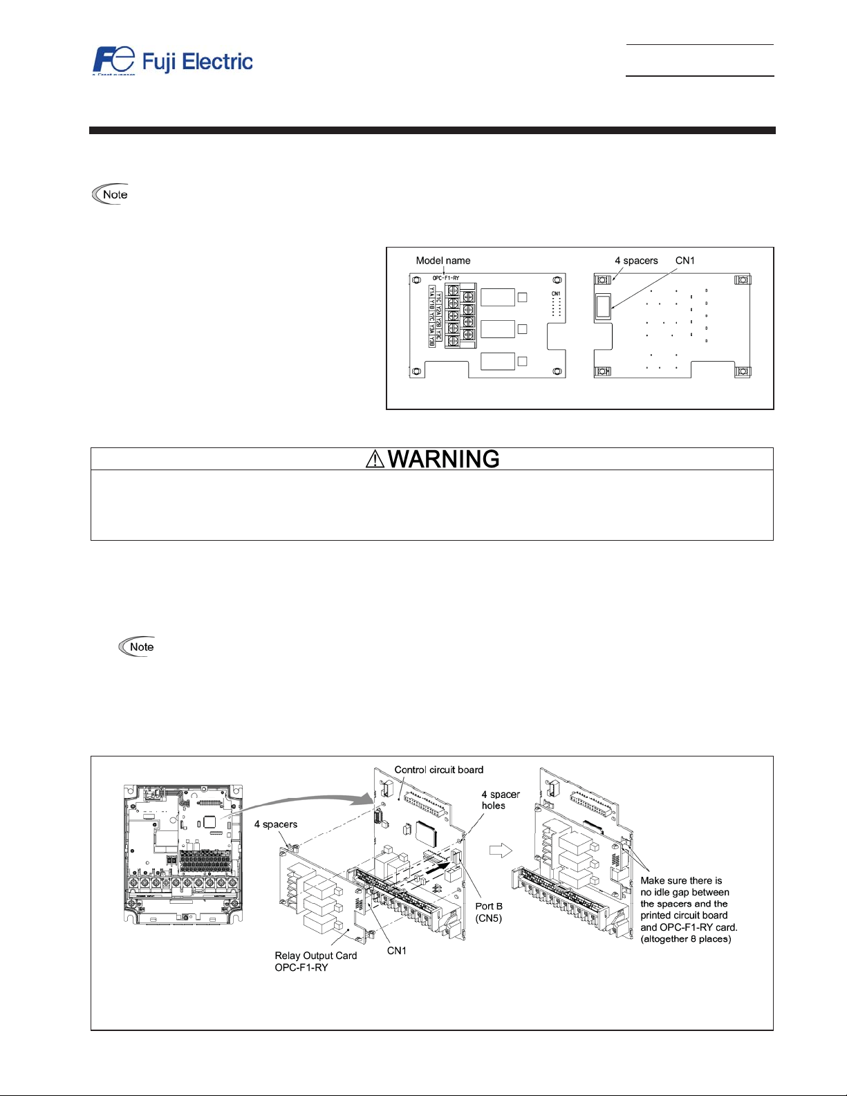
(3) The model name "OPC-F1-RY" is printed on the
Relay Output Card. (See Figure 1.)
If you suspect the product is not working properly or if
you have any questions about your product, contact your
Fuji Electric representative.
2. Installation
Turn the power off and wait for at least five minutes for models of 40 HP or below, or ten minutes for models of 50 HP or above,
before starting installation. Further, check that the LED monitor is unlit, and check the DC link circuit voltage between the P (+) and
N (-) terminals to be lower than 25 VDC.
Otherwise, electric shock could occur.
Figure 1 Front of Card Figure 2 Back of Card
(1) Remove the cover from the inverter and expose the control circuit board (See Figure 3.).
To remove the inverter cover, refer to Section 2.3 "Wiring" of FRENIC-Eco Instruction Manual (INR-SI47-1225-E). For
capacities of 50 HP or above, open also the keypad enclosure.
(2) Insert the four spacers and CN1 on the back of the OPC-F1-RY (as shown in Figure 2) into the spacer holes and Port B (CN5) on
the control circuit board in the inverter (Figure 4).
Visually check that the spacers and CN1 are firmly inserted (See Figure 5.).
(3) Wire on OPC-F1-RY.
Refer to Section 3 "Wiring."
(4) Put the cover back to the inverter.
To put back the inverter cover, refer to Section 2.3 "Wiring" of FRENIC-Eco Instruction Manual (INR-SI47-1225-E). For
capacities of 50 HP or above, close also the keypad enclosure.
Figure 3 In the case of
FRN010F1S-2U thru
FRN020F1S-2U
Figure 4 Mounting Relay Output Card Figure 5 Mounting Completed
- 1 -
Page 2

3. Wiring
t
In general, sheaths and covers of the control signal cables and wires are not specifically designed to withstand a high electric field
(i.e., reinforced insulation is not applied). Therefore, if a control signal cable or wire comes into direct contact with a live conductor of
the main circuit, the insulation of the sheath or the cover might break down, which would expose the signal wire to a high voltage of
the main circuit. Make sure that the control signal cables and wires will not come into contact with live conductors of the main circuit.
Failure to observe these precautions could cause electric shock and/or an accident.
Noise may be emitted from the inverter, motor and wires.
Implement appropriate measure to prevent the nearby sensors and devices from malfunctioning due to such noise.
An accident could occur.
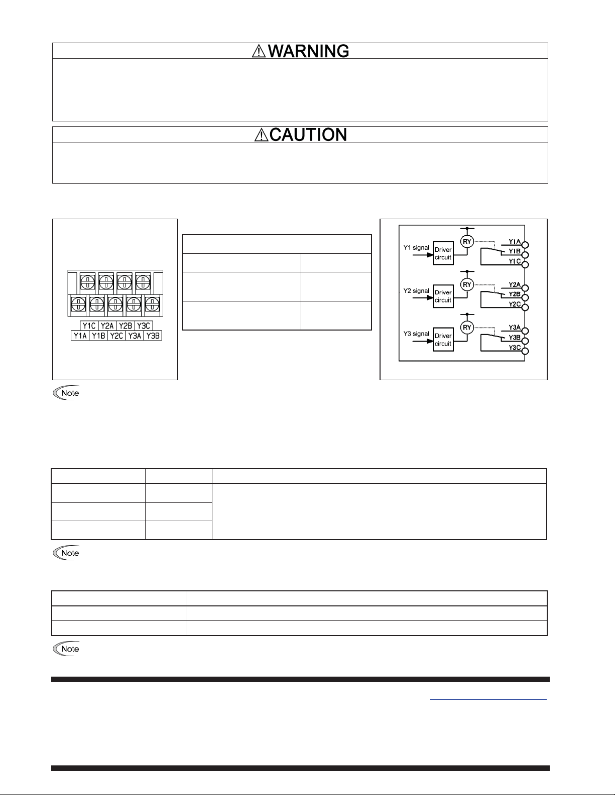
Wire properly, referring to the terminal allocation and symbol diagram, the internal block diagram, and the terminal and wiring
specification table shown below.
Terminal Size & Recommended Wire Gauge
Terminal Size M3
0.7 N·m
(0.52 lbf·ft)
AWG 18
( 0.75 mm
2
)
Figure 7 Internal Block Diagram
Figure 6 Terminal Allocation
and Symbol Diagram
Tightening Torque
Recommended Wire
Gauge*
* A 600 V HIV insulated wire with allowable temperature
of 75qC(167qF) is recommended. An ambient
temperature of 50qC(122qF) is assumed.
To prevent noise from causing malfunctioning, separate signal wires for the control circuit as far apart as possible from those for
the main circuits. Also, inside the inverter, bundle and fix the wires for the control circuit so that they do not come into direc
contact with live parts of the main circuits (for example, the main circuit terminal block).
Terminal Assignment
The relay output terminals are assigned as shown below. Basically, the meaning of the relay outputs follows that of the transistor outputs
Y1 to Y3, which is determined by their corresponding function codes.
Terminal Symbol Terminal Name Description
Y1A/Y1B/Y1C Relay Output 1
Y2A/Y2B/Y2C Relay Output 2
Y3A/Y3B/Y3C Relay Output 3
Relay outputs directly linked to transistor outputs Y1 to Y3. Each relay is excited when its
corresponding signal (Y1, Y2, or Y3) is ON. When excited, its output Y1A - Y1C, Y2A - Y2C,
or Y3A - Y3C is made, and Y1B - Y1C, Y2B - Y2C, or Y3B - Y3C is broken, respectively. In
this manner, the signals corresponding to function codes E20 - E22 (inverter running,
speed/frequency equivalence, and motor overload early warning) can be output as contact
When the inverter's control power is OFF, all the B - C contact pairs are short-circuited. If you are using negative logic to realize
fail-safe operation, make sure that this does not cause any logic fault or confliction.
Electrical Specifications
Item Specification
Contact capacity 250 VAC, 0.3 A (cos ( = 0.3) or 48 VDC, 0.5 A (resistive load)
Contact life 200,000 operations (with ON/OFF intervals of 1 second)
If you anticipate frequent operations (ON/OFF switching) of relays (for example, if you deliberately use a signal for limiting the
inverter's output to control the main current), be sure to use the transistor signals at terminals Y1 through Y3.
Fuji Electric Systems Co., Ltd.
Fuji Electric Corp.of America
47520 Westinghouse Drive Fremont, CA 94539, U.S.A.
Tel.+1-510-440-1060 Fax.+1-510-440-1063
http://www.fujielectric.com/fecoa/
Toll-free support 1-888-900-FUJI(3854)
INR-SI47-0873-EU REV. 052010 Information subject to change without notice.
- 2 -
 Loading...