

Page 1

series
USER'S MANUAL
PULSE TRAIN OUTPUT POSITIONING
CONTROL MODULE
FEH215
Page 2

Preface
This User’s Manual explains the pulse train output
positioning control module.
Read this manual carefully to ensure correct operation.
eltiT .oNlaunaM stnetnoC
XS-XERCIM,noitcurtsnIlaunaMs'resU
HPSseires
s'resUXS-XERCIM,erawdraHlaunaM
HPSseires
,>noitcudortnI<niw003DlaunaMs'resU
seiresXS-XERCIM
,>ecnerefeR<niw003DlaunaMs'resU
seiresXS-XERCIM
dnammocgolanAlaunaMs'resU
,eludomdenibmoclortnocgninoitisop
HPSseiresXS-XERCIM
gninoitisopniartesluPlaunaMs'resU
XS-XERCIM,eludomdenibmoclortnoc
HPSseires
002HEF ehtfosnoitinifedmetsysdnaegaugnal,yromemehtsnialpxE
102HEFdnasnoitacificepseht,noitarugifnocmetsysehtsnialpxE
052HEF dnagnimmargorpeht,niw003DfosnoitarepocisabehtsnialpxE
152HEF snoitarepoehtfolladnaniw003DfonocidnaunemehtsnialpxE
312EHF lortnocgninoitisopdnammocgolanaehtfosnoitarepoehtsnialpxE
412HEF lortnocgninoitisopniarteslupehtfosnoitarepoehtsnialpxE
When using modules or peripheral devices, be sure to read
the corresponding user’s manuals listed below.
.seiresXS-XERCIM
.seiresXS-XERCIMehtniseludomfosnoitarepo
.seiresXS-XERCIMrofgnirotinom
.niw003Dfo
.eludomdenibmoc
.eludomdenibmoc
Notes
1. This manual may not be reproduced in whole or part in any form without prior written approval by the manufacturer.
2. The contents of this manual (including specifications) are subject to change without prior notice.
3. If you find any ambiguous or incorrect descriptions in this manual, please write them down (along with the manual No.
shown on the cover) and contact FUJI.
Page 3

Safety Precautions
Be sure to read the “Safety Precautions” thoroughly before
using the module.
Warning
Caution
Even some items indicated by “Caution” may also result in a
serious accident.
: Incorrect handling of the device may result in death or serious injury.
: Incorrect handling of the device may result in minor injury or physical damage.
Here, the safety precaution items are classified into
“Warning” and “Caution.”
Both safety instruction categories provide important
information. Be sure to strictly observe these instructions.
Warning
◊ Never touch any part of charged circuits as terminals and exposed metal portion while the power is turned ON. It may result
in an electric shock to theoperator.
◊ Turn OFF the power before mounting, dismounting, wiring, maintaining or checking, otherwise, electric shock, erratic
operation or troubles might occur.
◊ Place the emergency stop circuit, interlock circuit or the like for safety outside the PC. A failure of PC might break or cause
problems to the machine.
◊ Do not connect in reverse polarity, charge (except rechargeable ones), disassemble, heat, throw in fire or short-circuit the
batteries, otherwise, they might burst or take fire.
◊ If batteries have any deformation, spilled fluids, or other abnormality, do not use them. The use of such batteries might cause
explosion or firing.
◊ Do not open the FG terminal with the LG-FG short circuited. (It must be grounded, otherwise it might cause electric shock.)
Page 4

Safety Precautions
Caution
◊ Do not use one found damaged or deformed when unpacked, otherwise, failure or erratic operation might be caused.
◊ Do not shock the product by dropping or tipping it over, otherwise, it might be damaged or troubled.
◊ Follow the directions of the operating instructions when mounting the product. If mounting is improper, the product might
drop or develop problems or erratic operations.
◊ Use the rated voltage and current mentioned in the operating instructions and manual. Use beyond the rated values might
cause fire, erratic operation or failure.
◊ Operate (keep) in the environment specified in the operating instructions and manual. High temperature, high humidity,
condensation, dust, corrosive gases, oil, organic solvents, excessive vibration or shock might cause electric shock, fire,
erratic operation or failure.
◊ Select a wire size to suit the applied voltage and carrying current. Tighten the wire terminals to the specified torque.
Inappropriate wiring or tightening might cause fire, malfunction, failure, or might cause the product to drop from its
mounting.
◊ Contaminants, wiring chips, iron powder or other foreign matter must not enter the device when installing it, otherwise,
erratic operation or failure might occur.
◊ Remove the dust-cover seals of modules after wiring, otherwise, fire, accidents, failure or fault might occur.
◊ Connect the ground terminal to the ground, otherwise, an erratic operation might occur.
◊ Periodically make sure the terminal screws and mounting screws are securely tightened.
Operation at a loosened status might cause fire or erratic operation.
◊ Put the furnished connector covers on unused connectors, otherwise, failure or erratic operation might occur.
◊ Install the furnished terminal cover on the terminal block, otherwise, electric shock or fire might occur.
◊ Sufficiently make sure of safety before program change, forced output, starting, stopping or anything else during a run.
The wrong operation might break or cause machine problems.
◊ Engage the loader connector in a correct orientation, otherwise, an erratic operation might occur.
◊ Before touching the PC, discharge any static electricity that may have been collected on your body. To discharge it, touch
a grounded metallic object. Static electricity might cause erratic operation or failure of the module.
◊ Be sure to install the electrical wiring correctly and securely, observing the operating instructions and manual. Wrong or
loose wiring might cause fire, accidents, or failure.
◊ When disengaging the plug from the outlet, do not pull the cord, otherwiase, break of cable might cause fire or failure.
◊ Do not attempt to change system configurations (such as installing or removing I/O modules) while the power is ON,
otherwise, failure or erratic operation might occur.
◊ Do not attemp to repair the module by yourself -- contact your Fuji Electric agent. When replacing the batteries, correctly
and securely connect the battery connectors, otherwise, fire, accidents or failure might occure.
◊ To clean the module, turn power off and wipe the module with a cloth moistened with warm water. Do not use thinner or
other organic solvents, as the module surface might become deformed or discolored.
◊ Do not remodel or disassemble the product, otherwise, a failure might occur.
◊ Follow the regulations of industrial wastes when the device is to be discarded.
◊ The modules covered in these operating instructions have not been designed or manufactured for use in equipment or
systems which, in the event of failure, can lead to loss of human life.
◊ If you intend to use the modules covered in these operating instructions for special applications, such as for nuclear
energy control, aerospace, medical, or transportation, please consult your Fuji Electric agent.
◊ Be sure to provide protective measures when using the module covered in these operating instructions in equipment
which, in the event of failure, may lead to loss of human life or other grave results.
Page 5

nodetnirP .oNlaunaM* stnetnocnoisiveR
9991yaM512HEFnoitidetsriF
Revision
.revocehtnonwohssi.oNlaunaM*
Page 6

Contents
Preface
Safety Precautions
Revision
Contents
Page
Section 1 General ...............................................................................................1-1
1-1 Precautions.............................................................................................................................................1-1
1-2 Functional Overview ..............................................................................................................................1-2
1-2-1 Overview of NP1F-HP2 functions ................................................................................................................. 1-2
1-2-2 Overview of NP2F-LEV functions ................................................................................................................. 1-3
Section 2 System Configuration .......................................................................2-1
2-1 Configuration of Peripheral Equipment...............................................................................................2-1
2-2 Applied System ......................................................................................................................................2-2
2-2-1 Applicable CPU ............................................................................................................................................. 2-2
2-2-2 Applied system configuration ........................................................................................................................ 2-2
2-3 Loader and Software Modules to be used...........................................................................................2-3
Section 3 Specifications
3-1 General Specifications (NP1F-HP2) .....................................................................................................3-1
3-1-1 General specifications (NP2F-LEV) .............................................................................................................. 3-2
3-2 Specifications (NP1F-HP2) .....................................................................................................................3-3
3-2-1 Specifications (NP2F-LEV) ........................................................................................................................... 3-3
3-3 Names......................................................................................................................................................3-4
3-3-1 NP1F-HP2 (for 2 axes).................................................................................................................................. 3-4
3-3-2 NP2F-LEV (Signal converter) ....................................................................................................................... 3-6
3-4 Dimensions .............................................................................................................................................3-8
3-4-1 NP1F-HP2 (for 2 axes).................................................................................................................................. 3-8
3-4-2 NP2F-LEV (Signal converter) ....................................................................................................................... 3-8
Section 4 Wiring..................................................................................................4-1
4-1 Mounting Precautions............................................................................................................................4-1
4-1-1 Number of mountable modules (NP1F-HP2)................................................................................................ 4-1
4-1-2 Wiring precautions......................................................................................................................................... 4-2
4-1-3 Wiring example of the external wiring connector.......................................................................................... 4-2
4-2 Connector Pin Layout for the External Connection (NP1F-HP2) ......................................................4-3
4-2-1 External I/O signal specifications (NP1F-HP2)............................................................................................. 4-4
4-3 Connector Pin Layout for the External Connection (NP2F-LEV) ....................................................4-11
4-3-1 External I/O signal specifications (NP2F-LEV) ........................................................................................... 4-12
4-3-2 External I/O signal interface (NP2F-LEV) ................................................................................................... 4-13
4-4 Connecting............................................................................................................................................4-15
4-4-1 Connecting sample of a servo motor .......................................................................................................... 4-15
4-5 I/O Wiring...............................................................................................................................................4-18
Section 5 Memory Map ......................................................................................5-1
5-1 NP1F-HP2 Memory Map (Internal Memory List) ..................................................................................5-1
5-2 I/O Area of NP1F-HP2.............................................................................................................................5-2
5-2-1 NP1F-HP2 (read area: address No. 0 to No. 7) ........................................................................................... 5-3
Page 7

Contents
5-2-2 NP1F-HP2 (Write area, address Nos. 8 to 15) ........................................................................................... 5-14
5-3 Setting Method and Effective Bits ......................................................................................................5-32
Section 6 Parameter s (Registers) .....................................................................6-1
6-1 Parameters (Registers) ..........................................................................................................................6-1
6-2 Relationship between Parameters (Registers)....................................................................................6-2
6-3 Detailed Description of Parameters (Registers) .................................................................................6-4
Section 7 Positioning Function.........................................................................7-1
7-1 Positioning Function of the Pulse Train Output Positioning Control Module (NP1F-HP2).............7-1
7-2 Functions of Pulse Train Output Positioning Control Module (NP1F-HP2)......................................7-2
7-2-1 Command pulse count control ...................................................................................................................... 7-3
7-2-2 Command pulse frequency control ............................................................................................................... 7-4
7-2-3 Trapezoidal acceleration/deceler ation .......................................................................................................... 7-5
7-2-4 Automatic deceleration point calculation ...................................................................................................... 7-7
7-2-5 Deceleration point setting.............................................................................................................................. 7-8
7-2-6 Continuous frequency rewriting .................................................................................................................... 7-9
7-2-7 Setti n g d a t a t o a r e g i s t e r ............................................................................................................................... 7-9
7-2-8 Data reading from register .......................................................................................................................... 7-10
7-2-9 Current value data reading.......................................................................................................................... 7-11
7-2-10 Manual operation....................................................................................................................................... 7-12
7-2-11 Original point return motion ....................................................................................................................... 7-12
7-2-12 Positioning operation................................................................................................................................. 7-14
7-2-13 Interrupt point positioning motion.............................................................................................................. 7-15
7-2-14 Deceleration-and-stop/quick stop motion ................................................................................................. 7-16
7-2-15 Operation when an emergency stop error has been detected .................................................................7-17
7-2-16 Operation when an ± OT error has been detected ................................................................................... 7-18
7-2-17 Command pulse counting ......................................................................................................................... 7-20
7-2-18 Operation when a transmission error has been detected ........................................................................ 7-21
Section 8 Troubleshooting.................................................................................8-1
8-1 LED Indication ........................................................................................................................................8-1
8-2 Error Indication.......................................................................................................................................8-2
Appendix........................................................................................................App.-1
Appendix-1 Parameters..........................................................................................................................App.-1
Appendix-2 Memory map.......................................................................................................................App.-2
Appendix-3 Terminology ........................................................................................................................App.-3
Appendix-4 Current Consumption and Mass of Modules in MICREX-SX Series.............................App.-5
Page 8

Section 1 General
Page
1-1 Precautions .............................................................................................................. 1-1
(1) Handling precautions as precision device .......................................................................................... 1-1
(2) Precautions concerning operating conditions and environment ......................................................... 1-1
1-2 Functional Overview................................................................................................ 1-2
1-2-1 Overview of NP1F-HP2 functions ......................................................................................1-2
1-2-2 Overview of NP2F-LEV functions ...................................................................................... 1-3
Page 9

Section 1 General
1-1 Precautions
The NP1F-HP2 is a pulse train output positioning control
module which is connected to a high-performance CPU
module and a standard CPU module of a MICREX-SX
Precautions for using the NP1F-HP2 are as follows:
(1) Handling precautions as precision device
1) Do not drop the device.
2) Avoid installing the device in places subject to
strong vibrations.
3) Avoid installing the device in places where
harmful gas (corrosive gas) exists.
4) Avoid installing the device within the same panel
as high-tension (3000 V or 6000 V
or more) devices.
5) Avoid sharing the same power supply with
equipment which produces high noise
(e.g. inverter).
6) Avoid using the device in places where the
temperature is too high or low, or the
humidity is too high.
Operating ambient temperature: 0 to 55°C
Operating ambient humidity: 20 to 95% RH
7) In places with extremely low humidity, excessive
static electricity tends to build up.
When you touch the NP1F-HP2 in such an
environment, be sure to touch a metal
ground in advance in order to discharge the static
electricity which is charged on your body.
series via an SX bus. It is used in combination with a pulse
train input command-type servo amplifier + motor or with a
stepping motor driver to perform high-accuracy positioning.
(2) Precautions concerning operating conditions and
environment
When the NP1F-HP2 is used in the following conditions or
environment, secure enough margin for the rated
specifications and functions (performance), take sufficient
fail-safe measures, and be sure to consult with personnel at
your Fuji Electric sales office.
1) Storage or use in conditions or an environment
which is not described in the operating
instructions or user’s manual.
2) Applications in nuclear power generation control,
railways, aircraft, railcars, incinerator equipment,
medical facilities,amusement machines, safety
devices, etc.
3) Applications where a great effect on human life or
property may be anticipated and a high degree
safety is required.
1-1
Page 10

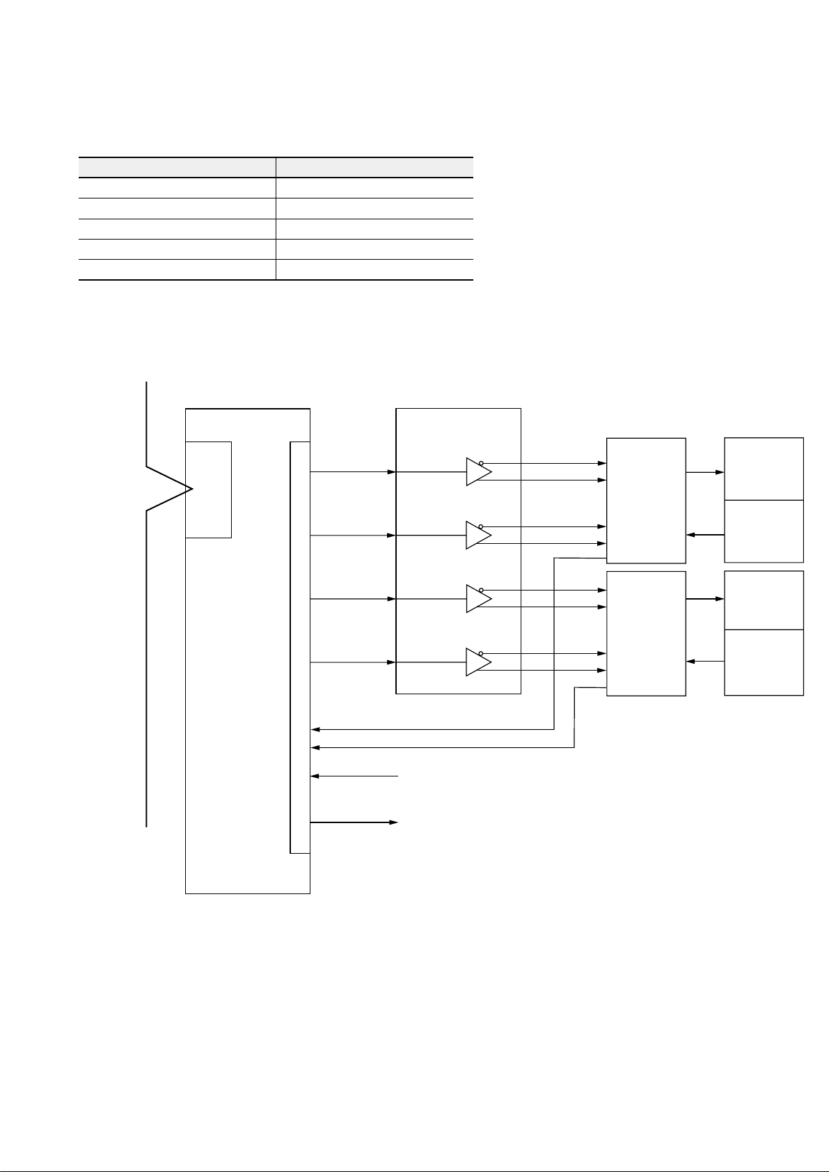
1-2 Functional Overview
1-2-1 Overview of NP1F-HP2 functions
metI noitpircseD
sexalortnocforebmuN
epyttuptuO
ycneuqerfdnammoc.xaM
citsiretcarahcnoitareleced/noitareleccA
tniopnoitarelecedfonoitaluclaC
)F/Ilaires(F/IedisUPC )sdrow61:latot,sdrow8:tuptuo,sdrow8:tupni(2PH-F1PN
A sample connection configuration of the NP1F-HP2 is shown
below:
Sample connection configuration of the NP1F-HP2
2
zHk052
)eslupesrever+eslupdrawrof(tuptuoniartesluprotcellocnepO
noitareleced/noitareleccaladiozeparT
noitaluclaccitamotuA
SX bus
NP1F-HP2
Serial I/F
X-axis forward/reverse pulse
Feedback pulse phase-Z
External I/Fs
Y-axis forward/reverse pulse
Timing output (TIM)
Servo
amplifier
Stepping
driver
DI : X axis (EMG, ±OT, origin LS, interrupt (5 points))
DO: Command output from CPU module (2 points)
Motor
Encoder
Motor
1-2
Page 11
1-2-2 Overview of NP2F-LEV functions
metI noitpircseD
slennahcnoisrevnocforebmuN)sexa4rof(4
epyttupnItupnirotcellocnepO
ycneuqerftupnIzHM1
epyttuptuO)revirdenil(langislaitnereffiD
ycneuqerftuptuOzHM1
A sample connection configuration of NP2F-LEV and NP1F-HP2
is shown below:
Sample connection configuration of the NP2F-LEV
1-2 Functional Overview
SX bus
NP1F-HP2
Serial I/F
X-axis
forward pulse
X-axis
External I/Fs
reverse pulse
Y-axis
forward pulse
Y-axis
reverse pulse
CH1 phase-Z
CH2 phase-Z
NP2F-LEV
Servo
amplifier
X-axis
differential
input
Servo
amplifier
Y-axis
differential
input
DI: X-/Y-axis (5 points/axis, EMG, ±OT, origin LS, interrupt)
DO: Command output from CPU module (2 points/axis)
Motor
Encoder
Motor
Encoder
1-3
Page 12

Section 2 System Configuration
Page
2-1 Configuration of Peripheral Equipment................................................................. 2-1
2-2 Applied System ........................................................................................................ 2-2
2-2-1 Applicable CPU .................................................................................................................. 2-2
2-2-2 Applied system configuration .............................................................................................2-2
(1) For a 2-axis system ............................................................................................................................ 2-2
(2) Sample extensions (for 8-axis system) ............................................................................................... 2-2
2-3 Loader and Software Modules to be used............................................................. 2-3
Page 13
Section 2 System Configuration
2-1 Configuration of Peripheral Equipment
The overall configuration of the NP1F-HP2 including a
MICREX-SX series CPU and peripheral equipment is shown
below:
Overall configuration
MICREX-SX CPU
module
NP1PSNP1PH-
Various-type
FBs for
positioning
D300win
positioning
loader software
SX bus
Positioning
control module
NP1F-HP2
Timing
output
*1
Signal converter
NP2F-LEV
Phase-Z
Stepping motor
driver
Servo
amplifier
Stepping motor
: Area covered by this manual
Motor
Encoder
Precaution:
This module only contains the basic functions for positioning processing. Motion-related functions (manual motion, original
point return motion, etc.) are processed by the expansion FB (function block) which is integrated into the MICREX-SX series
CPU module.
*1 When this module is combined with a differential signal input-type servo amplifier or a stepping motor driver, a signal
converter is needed.
2-1
Page 14
2-2 Applied System
2-2-1 Applicable CPU
The NP1F-HP2 can be used with a MICREX-SX series CPU.
1) High-performance CPU module ..... NP1PS-
2) Standard CPU module ................... NP1PH-
3)
4)
5)
2-2-2 Applied system configuration
The NP1F-HP2 is connected to the CPU module via an SX bus.
Sample connections are shown below:
(1) For a 2-axis system
Power supply module : NP1S-22
CPU module : NP1PSBase board : NP1BS-06
Positioning control module : NP1F-HP2
Power supply
module
Positioning
CPU module
control module
Input
module
Output
Input module : NP1X1606-W
module
Output module : NP1Y16R-08
(2) Sample extensions (for 8-axis system)
Positioning
module
control module
Output
module
Power supply
module
Power supply
module
: SX bus terminating plug
(NP8B-BP)
CPU module
Input
For how to mount the modules, refer to Section 4.
Input
Positioning
control module
Positioning
Positioning
control module
Power supply module : NP1S-22
CPU module : NP1PSBase board : NP1BS-06
Positioning control module : NP1F-HP2
Extension cable : NP1C-P3
module
Input module : NP1X1606-W
Output module : NP1Y16R-08
control module
2-2
Page 15

2-3 Loader and Software Modules to be used
The following loader and software modules are necessary to
operate the NP1F-HP2.
erawtfosredaoL epyT noitacilppA
gnimmargorpdetpadaniw003D
loottroppus
erawtfoS epyT noitacilppA
)BF(kcolbnoitcnufnoisnapxE
lortnocgninoitisoprofegakcap
DES-H4PN .UPCehtrofsmargorpnoitacilpparotinom/etirw/daer/retsigeR
FPTP-N4PN detalopretni-isauq,noitareposixatnednepednirofsmargorpnoitacilppA
.detcelesebnacnrutertnioplanigirodnanoitarepolaunam,noitom
2-3
Page 16

Section 3 Specifications
Page
3-1 General Specifications (NP1F-HP2) ....................................................................... 3-1
3-1-1 General specifications (NP2F-LEV) ................................................................................... 3-2
3-2 Specifications (NP1F-HP2)....................................................................................... 3-3
3-2-1 Specifications (NP2F-LEV) ................................................................................................3-3
3-3 Names .......................................................................................................................3-4
3-3-1 NP1F-HP2 (for 2 axes) ......................................................................................................3-4
3-3-2 NP2F-LEV (Signal converter) ............................................................................................ 3-6
3-4 Dimensions...............................................................................................................3-8
3-4-1 NP1F-HP2 (for 2 axes) ......................................................................................................3-8
3-4-2 NP2F-LEV (Signal converter) ............................................................................................ 3-8
Page 17

metI noitacificepS
htgnertscirtceleiD )dnuorgemarfdnasniprotcennocO/Ineewteb(etunim1CAV0051
ecnatsisernoitalusnIm01 Ω )dnuorgemarfdnasniprotcennocO/Ineewteb(reggemCDV005htiweromro
tneibmagnitarepO
erutarepmet
erutarepmetegarotS07+ot02- ° C
lacisyhP
latnemnorivne
snoitidnoc
lacinahceM
ecivres
snoitidnoc
lacirtcelE
ecivres
snoitidnoc
ylppusrewoP
noitallatsnI
snoitidnoc
tsuD
noitarbiV s/m6.91:noitareleccatnatsnoC,mm51.0:edutilpmaflaH
kcohSs/m741:kaepnoitareleccA
egrahcsid
dleif
ylppus
gnilooCgniloocriA
ssaM
ytidimuhevitaleR )noitasnednoconHR%59ot5:noitidnoctropsnarT(noitasnednoconHR%59ot02
eergednoitulloP2
ytinumminoisorroC .retawroliognittuc,stnevloscinagrohtiwdeniatstoN.sesagevisorrocmorfeerF
edutitlagnitarepOlevelaesevobasselrom0002
erusserpcirehpsomtA
ytinummiesioN1htdiweslup,sn1emitesir,Vk1 µ )rotalumisesion(s
citatsortcelE
citengamortceleoidaR
rewoPlanretxE
tnerruclanretnI
noitpmusnoc
noitcurtsnoC )epytdetnuomlenaP(epytkcolbgnidliuB:2PH-F1PN
snoisnemiD)mm(09Dx501Hx53W:2PH-F1PN
Section 3 Specifications
3-1 General Specifications (NP1F-HP2)
55+ot0 ° C
tsudevitcudnocmorfeerF
)edutitlam0003ottnelaviuqe(eromroaPk07
2
,
2
.sexaralucidneprepyllautumeerhtfohcaerofsemiteerhT
:egrahcsidtcatnoC ± Vk6
:egrahcsidlaireA ± Vk8
)zHM0001otzHM08(m/V01
Am53,CDV42:O/IroF
sselroAm59:2PH-F1PN
:2PH-F1PNg081.xorppA
.sruohxislatot,sexaralucidneprepyllautumeerhtfohcaerofsruohowT
3-1
Page 18

3-1 General Specifications (NP1F-HP2)
3-1-1 General specifications (NP2F-LEV)
metI noitacificepS
dohtemnoitalosI detalosisiylppusrewoplanretxE,)langistuptuodnalangistupnineewteb(detalositoN
lacisyhP
latnemnorivne
snoitidnoc
lacinahceM
ecivres
snoitidnoc
lacirtcelE
ecivres
snoitidnoc
ylppusrewoPylppusrewoplanretxEAm04,CDV42:O/IroF
noitallatsnI
snoitidnoc
tsuD
noitarbiV
kcohS
dleif
gnilooC
ssaM
tneibmagnitarepO
erutarepmet
erutarepmetegarotS
ytidimuhevitaleR
eergednoitulloP
ytinumminoisorroC
edutitlagnitarepO
erusserpcirehpsomtA
ytinummiesioN1htdiweslup,sn1emitesir,Vk5.1 µ )rotalumisesion(s
egrahcsidcitatsortcelE
citengamortceleoidaR
noitcurtsnoC )epytdetnuomlenaP(epytkcolbgnidliuB:VEL-F2PN
snoisnemiD
55ot0 ° C
07+ot52- ° C
noitasnednoconHR%59ot02
tsudevitcudnocmorfeerF
2
2
s/m741:kaepnoitareleccA
:egrahcsidtcatnoC ± Vk6
:egrahcsidlaireA ± Vk8
)zHM0001otzHM08(m/V01
gniloocriA
g031.xorppA:VEL-F2PN
)noitasnednoconHR%59ot5:noitidnoctropsnarT(
.retawroliognittuc,,stnevloscinagrohtiwdeniatstoN.sesagevisorrocmorfeerF
levelaesevobasselrom0002
)edutitlam0003ottnelaviuqe(eromroaPk07
2
s/m6.91:noitareleccatnatsnoC,mm51.0:edutilpmaflaH
,
.sruohxislatot,sexaralucidneprepyllautumeerhtfohcaerofsruohowT
.sexaralucidneprepyllautumeerhtfohcaerofsemiteerhT
)mm(59Dx59Hx8.93W:VEL-F2PN
3-2
Page 19

metI noitacificepS
noitcurtsnoC)deipuccotols1(epyteludoM
sdrowdeipuccO )sdrow8:tuptuO,sdrow8:tupnI(2PH-F1PN
sexalortnocfo.oNsexa2
lortnocgninoitisoPpoolnepO
noitareleced/noitareleccA
scitsiretcarahc
atadnoitisoP2.xaM
dnammoC
deeps
noitcnuflortnoC )kcolBnoitcnuF(BFnoisnapxeehtybdellortnoC
epyttuptuOtuptuorotcellocnepO
rotautcanoitanibmoC noitcnuftupniniarteslupderaperpmetsysovreS
ycneuqerfdnammoCzHk052
3-2-1 Specifications (NP2F-LEV)
metI noitacificepS
noitcurtsnoC)deipuccotols1(epyteludoM
sexalortnocfo.oN)slennahc4rof(sexa4
langistupnI
langistuptuO
ycneuqerftupnIzHM1.xaM
epyttupnIrotcellocnepO
ycneuqerftuptuOzHM1.xaM
epyttuptuOlangislaitnereffiD
3-2 Specifications (NP1F-HP2)
)edomnoitarenegeslupni(noitareleced/noitareleccaladiozeparT
23
dnammoc/eslup1-
3-3
Page 20
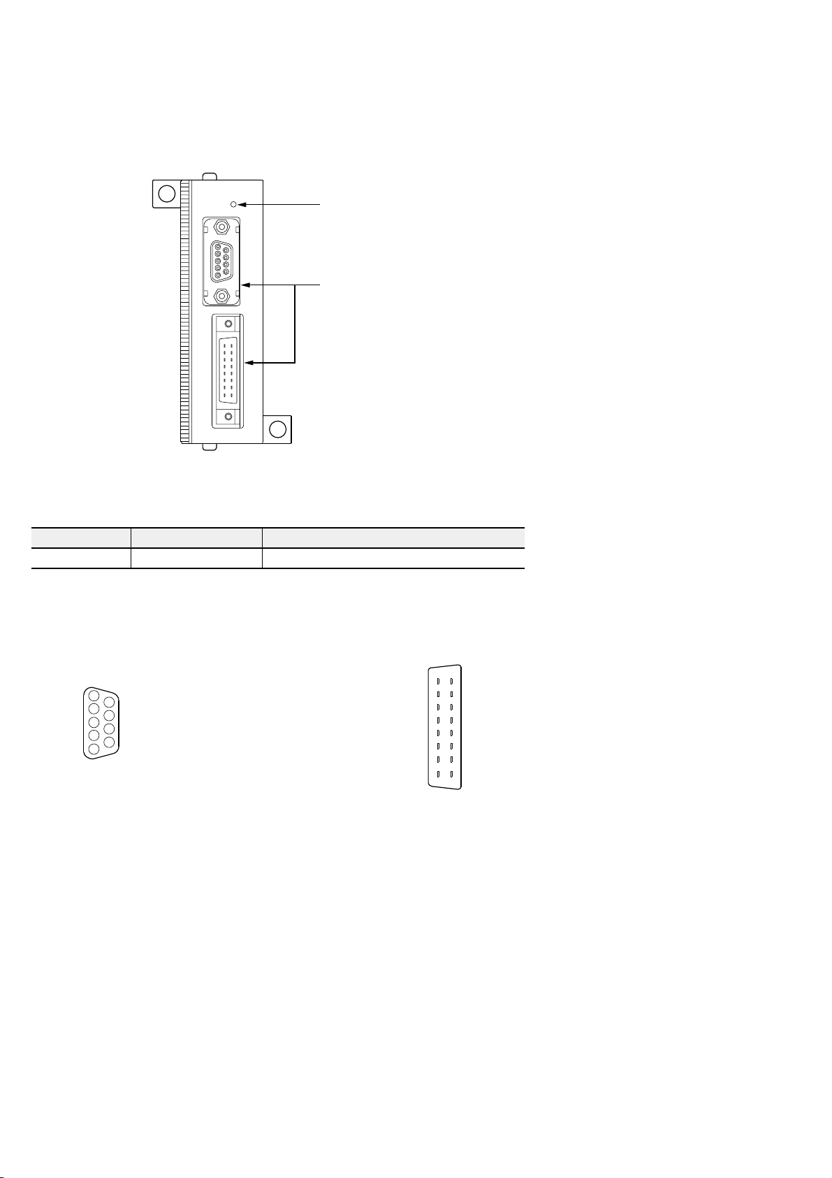
3-3 Names
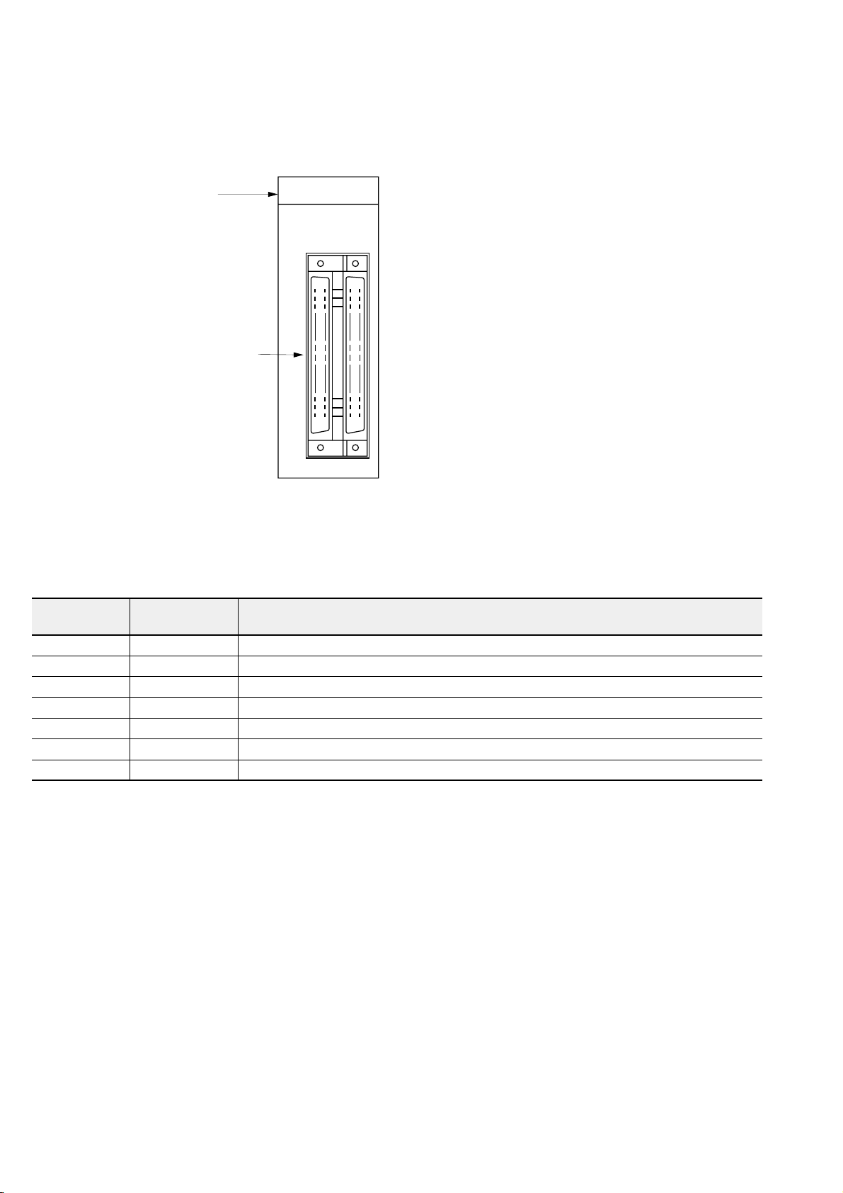
3-3-1 NP1F-HP2 (for 2 axes)
1) Status indication LED
ONL RDY
ERR ALM
CH1
EMG+OT-OT
CH2
2) External I/O signal connector
CH1 CH2
1) Status indication LED
This LED indicates the operation status and the error status
of NP1F-HP2. LED color means as shown below.
• Green: This is used to confirm the operation, not emergency.
• Red : Any fault status is detected, a state of emergency.
DELnoitacidnI
)2HC/1HC(
emaN
noitpircseD
)2HC/1HC(
)neerG(LNOlamronsubXS.lamronsisubXSnehwnosnruT
)deR(RRElamronbasubXS )revonoitaivedasaemaS(.subXSnisruccororrenanehwnosnruT
)neerG(YDRydaeR.lamronsieludomehtnehwnosnruT
)deR(MLArorrE .erawdrahehtniromargorpnoitacilppaehtnisruccororrenanehwnosnruT
)deR(GMEpotsycnegremE )etoN()tcatnocCN:langisO/IlanretxE(.NOsitupnipotsycnegremeehtnehwnosnruT
)deR(TO+levartrevO )etoN()tcatnocCN:langisO/IlanretxE(.NOsitupninoitceridsulpehtnehwnosnruT
)deR(TO-levartrevO )etoN()tcatnocCN:langisO/IlanretxE(.NOsitupninoitceridsunimehtnehwnosnruT
Note: Indication LEDs (EMG/±OT) operate with the external input signal. Only the status of input signals are indicated.
3-4
Page 21
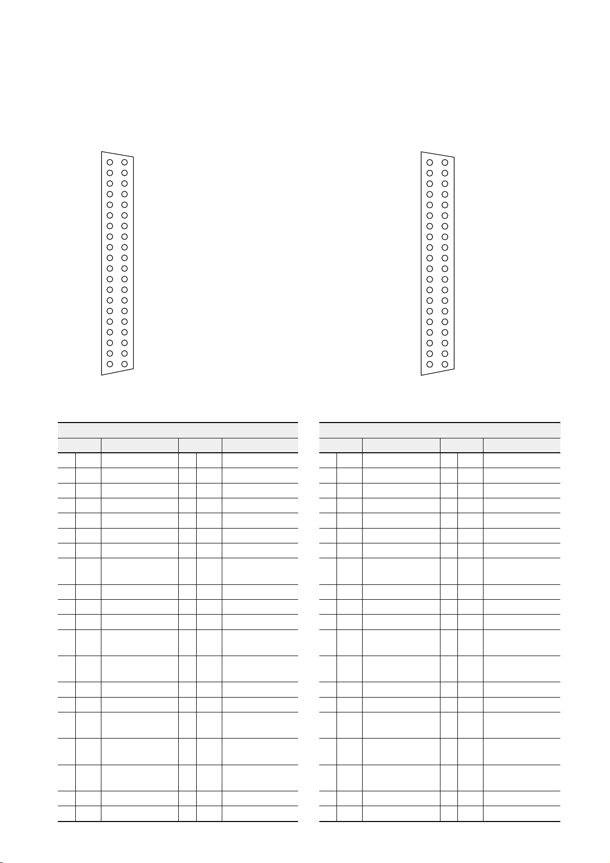
2) Connector pin layout for the external I/O signal
20
19
18
17
16
15
14
13
12
11
10
9
8
7
6
5
4
3
2
1
20
19
18
17
16
15
14
13
12
11
10
9
8
7
6
5
4
3
2
1
Connector pin layout (40-pin)
B/A
CH2
A front view A front view
B/A
CH1
3-3 Names
20
19
18
17
16
15
14
13
12
11
10
9
8
7
6
5
4
3
2
1
Connector pin layout (40-pin)
Signal name Signal name
1HC
.oNniP emanlangiS .oNniP emanlangiS
0202BCDV420202ACDV42
9191BCDV09191ACDV0
8181BMOC8181AMOC
7171BtupniTO-7171AtupniGME
6161BtupniTO+6161AtupniSLnigirO
5151B1MOCtupnI5151AtupnitpurretnI
4141B1MOCtupnI4141A1MOCtupnI
3131B
2121B2oD2121A1oD
1111BMOCtuptuO1111AMOCtuptuO
0101BMOC0101AMOC
99B
88B
77BC.N77AC.N
66BC.N66AC.N
55B
44B
33B
22BC.N22AC.N
11BC.N11AC.N
20
19
18
Usable connector
17
• NP1F-HP2 side
16
Connector···FCN-365P040-AU (Fujitsu)
15
Connector···N630-3651-T927 (Fujitsu)
14
13
For details of the connector, refer to “4-5 I/O Wiring.”
12
11
10
9
8
7
6
5
4
3
2
1
V42:tuptuoroF
CD
tuptuo
tuptuoesluP
MOC
DNG
MOC
MOC
3131A
eslupesreveR
99A
88A
eslupkcabdeeF
55A
44A
33A
CD
tuptuo
MOC
DNG
V42:tuptuoroF
eslupdrawroF
tuptuoesluP
eslupkcabdeeF
eslupkcabdeeF
Z-esahp
eslupkcabdeeF
Z-esahp*
2HC
.oNniP emanlangiS .oNniP emanlangiS
0202BCDV420202ACDV42
9191BCDV09191ACDV0
8181BMOC8181AMOC
7171BtupniTO-7171AtupniGME
6161BtupniTO+6161AtupniSLnigirO
5151B2MOCtupnI5151AtupnitpurretnI
4141B2MOCtupnI4141A2MOCtupnI
3131B
2121B2oD2121A1oD
1111BMOCtuptuO1111AMOCtuptuO
0101BMOC0101AMOC
99B
88B
77BC.N77AC.N
66BC.N66AC.N
55B
44B
33B
22BC.N22AC.N
11BC.N11AC.N
CD
tuptuo
MOC
DNG
MOC
MOC
V42:tuptuoroF
3131A
eslupesreveR
99A
tuptuoesluP
88A
eslupkcabdeeF
55A
44A
33A
V42:tuptuoroF
CD
eslupdrawroF
tuptuo
tuptuoesluP
MOC
eslupkcabdeeF
DNG
eslupkcabdeeF
Z-esahp
eslupkcabdeeF
Z-esahp*
3-5
Page 22
3-3 Names
3-3-2 NP2F-LEV (Signal converter)
PWR
1) Status indication LED
2) External I/O signal connector
LEV
1) Status indication LED
Status indication LED of NP2F-LEV
DELnoitacidnI emaN noitpircseD
)neerG(RWPylppusrewoplamroN.lamronsirewopCDV42nehwnosnruT
2) Connector pin layout for the external I/O signal
A front view (the upper side) A front view (the lower side)
Connector pin layout (9-pin) Connector pin layout (16-pin)
1
1
2
3
4
5
9
8
7
6
2
3
4
5
6
7
8
9
10
11
12
13
14
15
16
Usable connector Usable connector
• NP2F-LEV side • NP2F-LEV side
Connector···DELC-J9SAF-10L6 (JAE made) Connector···FCN-365P016-AU (Fujitsu)
Use the following connector cover Use the following connector cover
Connector···DEM-9P (JAE made) Connector···FCN-361J016-AU (Fujitsu)
Cover··········DE-C1-J6 (JAE made) Cover··········FCN-360C016-E (Fujitsu)
3-6
Page 23

Signal name (the upper side) Signal name (the lower side)
.oNniP emanlangiS
1V0
2V0
3V0
4V0
5V0
6)1ON(tupnirotcellocnepO
7)2ON(tupnirotcellocnepO
8)3ON(tupnirotcellocnepO
9)4ON(tupnirotcellocnepO
.oNniP emanlangiS .oNniP emanlangiS
1A)P1ON(tuptuolaitnereffidV51B)N1ON(tuptuolaitnereffidV5
2A)P2ON(tuptuolaitnereffidV52B)N2ON(tuptuolaitnereffidV5
3A)P3ON(tuptuolaitnereffidV53B)N3ON(tuptuolaitnereffidV5
4A)P4ON(tuptuolaitnereffidV54B)N4ON(tuptuolaitnereffidV5
5AV5_DNG5BV5_DNG
6ACN6BCN
7A)V42_DNG(CDV07B)V42_DNG(CDV0
8ACDV428BCDV42
3-3 Names
3-7
Page 24
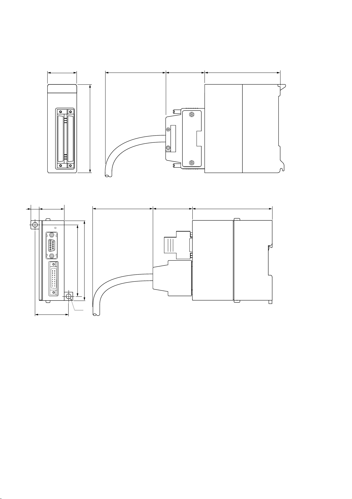
3-4 Dimensions
3-4-1 NP1F-HP2 (for 2 axes)
35
105
3-4-2 NP2F-LEV (Signal converter)
(75)
(46.5)
90
29.8
10
85
95
40
ø6
(75)
95(47.2)
3-8
Page 25

Section 4 Wiring
Page
4-1 Mounting Precautions .............................................................................................4-1
4-1-1 Number of mountable modules (NP1F-HP2) ..................................................................... 4-1
4-1-2 Wiring precautions .............................................................................................................4-2
4-1-3 Wiring example of the external wiring connector ...............................................................4-2
(1) Connector type ................................................................................................................................... 4-2
(2) Connector cover type......................................................................................................................... 4-2
4-2 Connector Pin Layout for the External Connection (NP1F-HP2).........................4-3
4-2-1 External I/O signal specifications (NP1F-HP2) ..................................................................4-4
4-3 Connector Pin Layout for the External Connection (NP2F-LEV).......................4-11
4-3-1 External I/O signal specifications (NP2F-LEV) ................................................................ 4-12
4-3-2 External I/O signal interface (NP2F-LEV) ........................................................................ 4-13
4-4 Connecting .............................................................................................................4-15
4-4-1 Connecting sample of a servo motor ...............................................................................4-15
(1) When the NP1F-HP2 generates the forward pulse or the reverse pulse.......................................... 4-15
(2) Forward pulse command, reverse pulse command .......................................................................... 4-15
(3) Connecting sample of FALDIC-II and NP1F-HP2 ............................................................................. 4-16
(4) Connecting sample of a stepping motor and NP1F-HP2 .................................................................. 4-17
4-5 I/O Wiring ................................................................................................................4-18
(1) Wiring of a connector type module
Page 26

4-1-1 Number of mountable modules (NP1F-HP2)
1) To mount the NP1F-HP2 to the base board where
the CPU module and the power supply module
are mounted on, take the following precautions.
1) Supplied power (Power supply module)
epyT )CDV42(tnerructuptuO
22-S1PNA64.1
)gnipoleveD(24-S1PNA64.1
2) Current consumption
Section 4 Wiring
4-1 Mounting Precautions
The number of mountable modules to the base
board in MICREX-SX is shown below.
)epyT(eludoM tnerruC
UPCecnamrofrep-hgiHA2.0
)2PM-F1PN(lortnocgninoitisopsexa2A590.0
)2AM-F1PN(lortnocgninoitisopsexa2A51.0
)2PH-F1PN(lortnocgninoitisopsexa2A590.0
)2CH-F1PN(retnuocdeeps-hgiHA580.0
)1SR-L1PN(noitacinummocesopruplareneGA11.0
)2CP-F1PN(dracCPA21.0
)1SA-L1PN(i-SAA1.0
)1PJ-L1PN(1-NCPJA31.0
)1LP-L1PN(knil-PA61.0
)1LT-L1PN(retsamknil-TA41.0
skrameR
noitpmusnoc
3) Current consumption of the positioning control
module
NP1F-HP2: 0.095A/ module
For the current consumption of I/O module, refer to
“Appendix-4 Current consumption and Mass of
Calculation method for the number of mountable modules
T-link master
CPU
1.46A - (0.2A + 0.14A + 0.07A)
0.095A (NP1F-HP2)
2) Installation conditions of the positioning control
module base on that conditions of MICREX-SX
Base board
= 11.05 = 11 module
MICREX-SX series.”
series. User’s Manual Hardware, MICREX-SX
series······FEH201
4-1
Page 27
4-1 Mounting Precautions
4-1-2 Wiring precautions
Precautions of wiring the positioning control module and the
external device are shown below.
1) The cable length between the positioning control
module and the driver varies with the driver type.
Confirm the specifications of the driver.
2) I/O wiring
· Do not bundle up or close the I/O cables to the
power cables or the main circuit cables.
· If these cables are closed near, separate the
ducts or wire them separately.
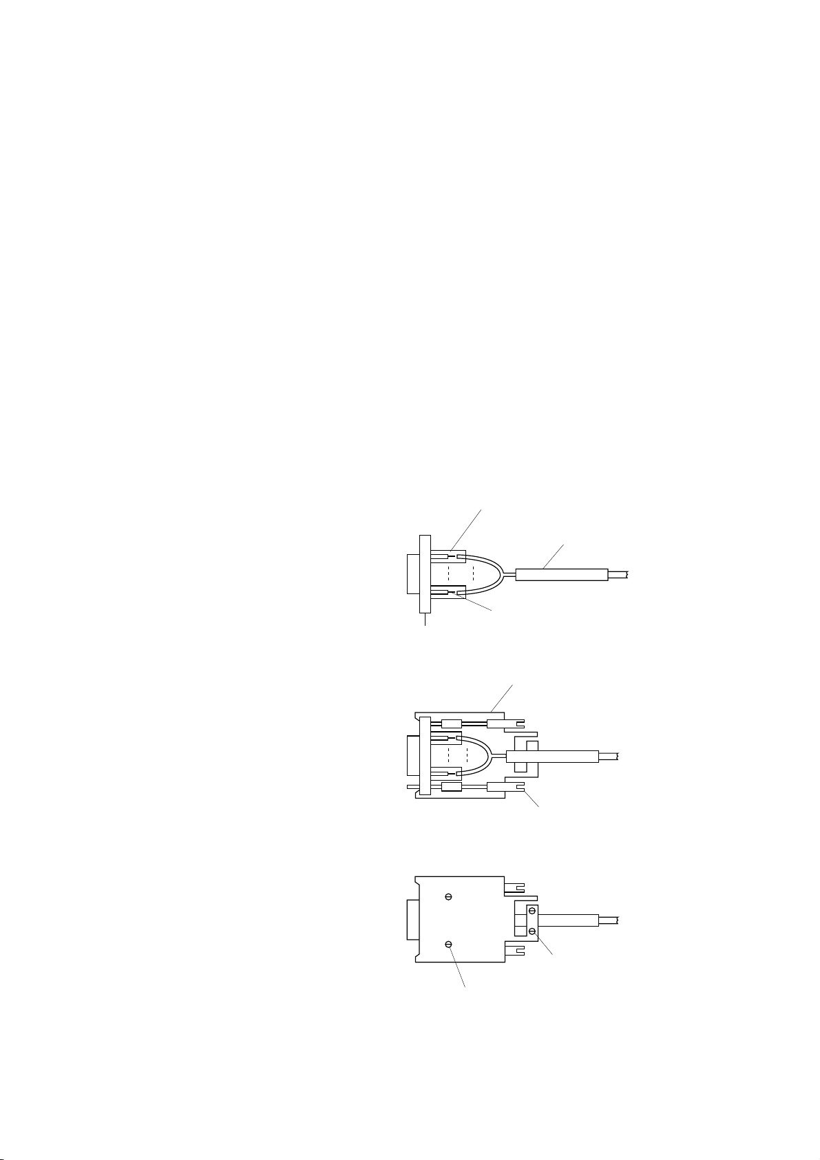
4-1-3 Wiring example of the external wiring
connector
(1) Connector type (2) Connector cover type
FCN-360C040-B (Fujitsu) FCN-361J040-AU (Fujitsu)
· If I/O wiring cannot be separated from the power
cables or the main circuit cables, bound shield
cables must be used and both ends of the shield
must be connected to SG (0V).
· To wire the pulse output, shielded cables must
be used.
· If the ducts are used for wiring, the ducts must
be grounded.
· To wire the open collector, the length of shielded
cable should be 3m or less.
1) Let the wires through the heat-shrinkable
tube. Let each wire through the insulation
tube, and solder them. The heatshrinkable tube is shrunk by a drier.
2)Mount the connector on the case (the
lower), and set the screw.
* Twist the wire in the connector case.
3) Put the case (the upper), and turn screws.
Insulation tube
Heat-shrinkable tube
Soldering
Connector
Case (the lower)
Screw
* For details of usable connector, refer to “4-5 I/O Wiring.”
4-2
Nut, screw and washer
Screw and nut
Page 28
2HC
.oNniP emanlangiS .oNniP emanlangiS
0202BCDV420202ACDV42
9191BCDV09191ACDV0
8181BMOC8181AMOC
7171BtupniTO-7171AtupniGME
6161BtupniTO+6161AtupniSLnigirO
5151B2MOCtupnI5151AtupnitpurretnI
4141B2MOCtupnI4141A2MOCtupnI
3131B
V42:tuptuoroF
CD
3131A
V42:tuptuoroF
CD
2121B2oD2121A1oD
1111BMOCtuptuO1111AMOCtuptuO
0101BMOC0101AMOC
99B
eslupesreveR
tuptuo
99A
eslupesreveR
tuptuo
88B
tuptuoesluP
MOC
88A
tuptuoesluP
MOC
77BC.N77AC.N
66BC.N66AC.N
55B
eslupkcabdeeF
DNG
55A
eslupkcabdeeF
DNG
44B
MOC
44A
eslupkcabdeeF
Z-esahp
33B
MOC
33A
eslupkcabdeeF
Z-esahp*
22BC.N22AC.N
11BC.N11AC.N
4-2 Connector Pin Layout for the
External Connection (NP1F-HP2)
CH1
20
19
18
17
16
15
14
13
12
11
10
9
8
7
6
5
4
3
2
1
B/A
Signal name Signal name
1HC
.oNniP emanlangiS .oNniP emanlangiS
0202BCDV420202ACDV42
9191BCDV09191ACDV0
8181BMOC8181AMOC
7171BtupniTO-7171AtupniGME
6161BtupniTO+6161AtupniSLnigirO
5151B1MOCtupnI5151AtupnitpurretnI
4141B1MOCtupnI4141A1MOCtupnI
3131B
2121B2oD2121A1oD
1111BMOCtuptuO1111AMOCtuptuO
0101BMOC0101AMOC
99B
88B
77BC.N77AC.N
66BC.N66AC.N
55B
44B
33B
22BC.N22AC.N
11BC.N11AC.N
*1 Do not use NC terminals as repeating terminals.
*2 Feedback pulse GND (A5, B5) are connected internal.
*3 Output COM (A11, B11) are connected internal.
CD
MOC
DNG
MOC
MOC
tuptuo
20
19
18
17
16
15
14
13
12
11
10
9
8
7
6
5
4
3
2
1
V42:tuptuoroF
eslupesreveR
tuptuoesluP
eslupkcabdeeF
Connector pin layout (40-pin)
· Usable connector
· NP1F-HP2 side
Connector···FCN-365P040-AU (Fujitsu)
Connector···N630-3651-T927 (Fujitsu)
For details of the connector, refer to “4-5 I/O Wiring.”
V42:tuptuoroF
eslupdrawroF
tuptuoesluP
eslupkcabdeeF
eslupkcabdeeF
Z-esahp
eslupkcabdeeF
Z-esahp*
3131A
99A
88A
55A
44A
33A
CD
tuptuo
MOC
DNG
20
19
18
17
16
15
14
13
12
11
10
9
8
7
6
5
4
3
2
1
CH2
20
19
18
17
16
15
14
13
12
11
10
9
8
7
6
5
4
3
2
1
B/A
4-3
Page 29

4-2 Connector Pin Lay out for the
External Connection (NP1F-HP2)
*4 For output: 24V DC (A13, B13) are connected internal.
*5 0V DC (A19, B19) are connected internal.
*6 24V DC (A20, B20) are connected internal.
*7 Input COM1 (A14, B14, B15) are connected internal. (Input COM1 is not connected to Input COM2.)
*8 Input COM2 (A14, B14, B15) are connected internal. (Input COM1 is not connected to Input COM2.)
*9 B3, B4, B5, A5, A10, B10, B11, A11, B18, A18, A19 and B19 are connected internal.
*10 For detail specifications of the above signals, refer to 4-2-1.
4-2-1 External I/O signal specifications (NP1F-HP2)
emanlangiS lobmyslanimreT .oNniprotcennoC noitcnuF noitacificepS
edis1HC edis2HC
Z-esahp*eslupkcabdeeF3A-1HC3A-2HClangisZ-esahpeslupkcabdeeffotupnICDV5egatlovtupnidetaR
eslupkcabdeeF
)tupnI(langis
tupnitpurretnI51A-1HC51A-2HCreggirtgninoitisoptpurretnifotupnICDV42egatlovtupnidetaR
tupniSLnigirO61A-1HC61A-2HCSLnigirofotupnI
tupniGME71A-1HC71A-2HC)tcatnocCN(potsycnegremefotupnI
langislanretxE
)tupnI(
tuptuoesluP
)tuptuO(langis
tuptuolanretxE
)tuptuO(langis
ylppusrewoP
)tupnI(
tupniTO+61B-1HC61B-2HC)tcatnocCN(noitceridsulpfotupnI
tupniTO-71B-1HC71B-2HC)tcatnocCN(noitceridsunimfotupnI
2,1MOCtupnI41A-1HC41A-2HClangistupnilanretxerofrewopnommoC
2,1MOCtupnI41B-1HC41B-2HClangistupnilanretxerofrewopnommoC
2,1MOCtupnI51B-1HC51B-2HClangistupnilanretxerofrewopnommoC
1OD21A-1HC21A-2HClangistuptuolanretxeroFtniop/A1.0.xaM
2OD21B-1HC21B-2HClangistuptuolanretxeroF
MOCtuptuO11A-1HC11A-2HCylppusrewoplanretxefonommoC
MOCtuptuO11B-1HC11B-2HCylppusrewoplanretxefonommoC
CDV42+02A-1HC02A-2HCylppusrewopV42+CDV42 ± %01
CDV42+02B-1HC02B-2HCylppusrewopV42+
CDV091A-1HC91A-2HCnommocylppusrewoP
CDV091B-1HC91B-2HCnommocylppusrewoP
Z-esahpeslupkcabdeeF4A-1HC4A-2HClangisZ-esahpeslupkcabdeeffotupnI
DNGeslupkcabdeeF5A-1HC5A-2HClangisV0eslupkcabdeeffotupnI
DNGeslupkcabdeeF5B-1HC5B-2HClangisV0eslupkcabdeeffotupnI
MOCtuptuoesluP8A-1HC8A-2HCMOCesluPtniop/Am05.xaM
tuptuoeslupdrawroF9A-1HC9A-2HCeslupnoitceridsulP
MOCtuptuoesluP8B-1HC8B-2HCMOCesluP
tuptuoeslupesreveR9B-1HC9B-2HCeslupnoitceridsuniM
CDV42:tuptuoroF31A-1HC31A-2HC)TUPNI(ylppusrewoplanretxE
CDV42:tuptuoroF31B-1HC31B-2HC)TUPNI(ylppusrewoplanretxE
tnerructupnidetaR
tniop/Am04
021ecnadepmitupnI Ω ro
ssel
ycneuqerfesluptupnI
sppk005.xaM
tnerructupnidetaR
tniop/Am06
k6.3ecnadepmitupnI Ω ro
ssel
ycneuqerfesluptuptuO
sppk052.xaM
A3.0tnerrucegruS
htgnertstnerrucegruS
sm01
4-4
Page 30
Signal name Circuit
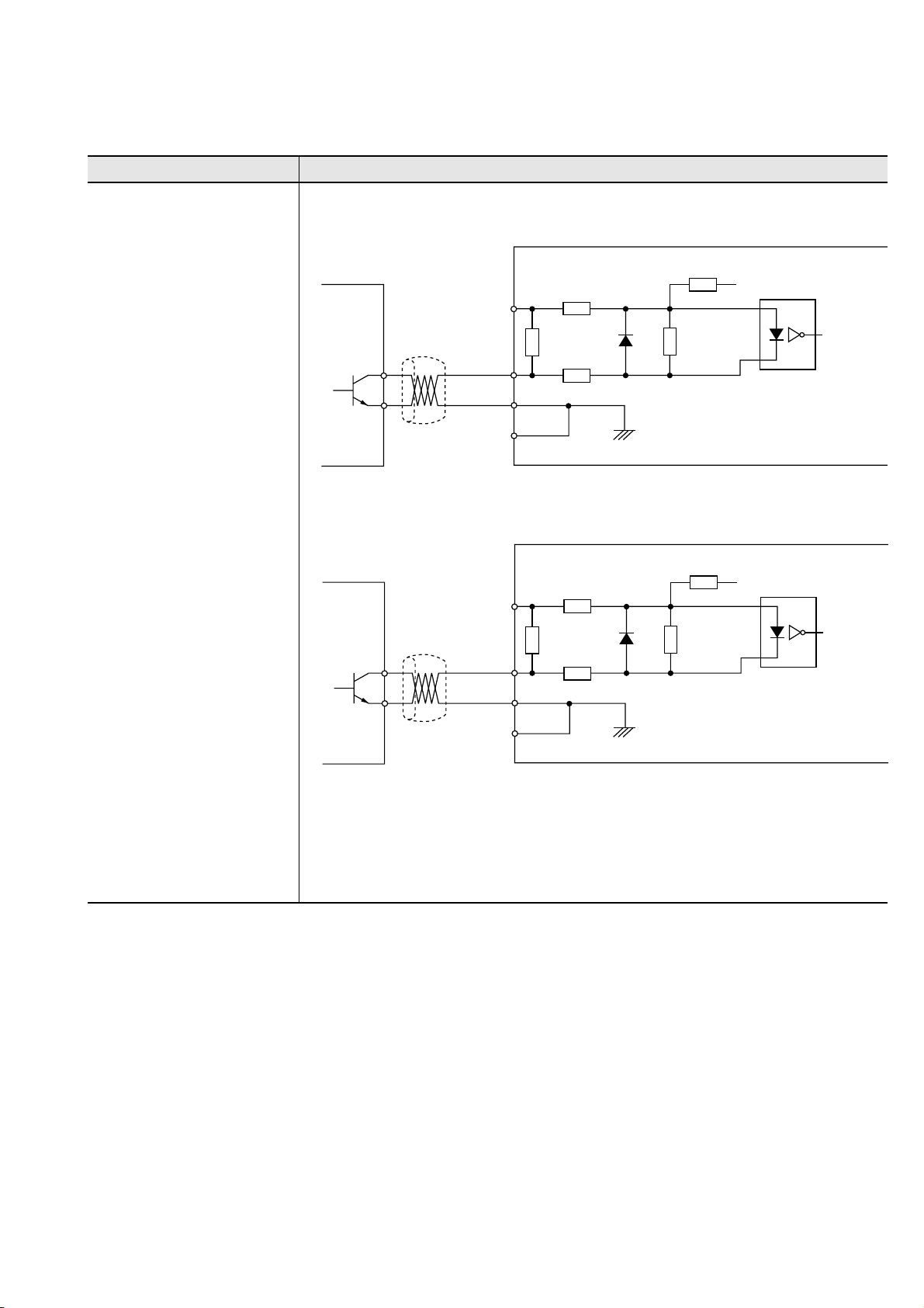
Feedback pulse signal
(input)
4-2 Connector Pin Layout for the
External Connection (NP1F-HP2)
Servo side
Phase-Z
Servo side
Phase-Z
CH1-A4
CH1-A3
CH1-A5
CH1-B5
CH2-A4
CH2-A3
CH2-A5
220Ω
220Ω
120Ω
120Ω
120Ω
120Ω
120Ω
510Ω
120Ω
510Ω
+5V
Phase-Z
CH1 side
+5V
Phase-Z
CH2-B5
When the feedback pulse signal is driven by a open collector.
CH2 side
4-5
Page 31

4-2 Connector Pin Lay out for the
External Connection (NP1F-HP2)
Signal name Circuit
Feedback pulse signal
(input)
Servo side
Phase-Z
Servo side
Phase-Z
CH1-A4
CH1-A3
CH1-A5
CH1-B5
CH2-A4
CH2-A3
CH2-A5
120Ω
220Ω
120Ω
220Ω
120Ω
120Ω
120Ω
510Ω
120Ω
510Ω
+5V
Phase-Z
CH1 side
+5V
Phase-Z
CH2-B5
When the feedback pulse signal is driven by a line driver.
CH2 side
4-6
Page 32

Signal name Circuit
4-2 Connector Pin Layout for the
External Connection (NP1F-HP2)
External input signal
(input)
-OT
+OT
Emergency
stop
Origin LS
Interrupt
+24V
CH1-A14
CH1-B17
CH1-B16
CH1-A17
CH1-A16
CH1-A15
1.8kΩ
1.8kΩ
1.8kΩ
1.8kΩ
1.8kΩ
1.8kΩ
1.8kΩ
1.8kΩ
1.8kΩ
1.8kΩ
820Ω
820Ω
820Ω
820Ω
820Ω
-OT
+OT
Emergency
stop
Origin LS
+24V
CH2-A14
CH2-B17
CH2-B16
CH2-A17
CH2-A16
1.8kΩ
1.8kΩ
1.8kΩ
1.8kΩ
1.8kΩ
1.8kΩ
1.8kΩ
1.8kΩ
CH1 side
820Ω
820Ω
820Ω
820Ω
Interrupt
CH2-A15
1.8kΩ
1.8kΩ
820Ω
CH2 side
4-7
Page 33

4-2 Connector Pin Lay out for the
External Connection (NP1F-HP2)
Signal name Circuit
Pulse output signal
(output)
1kΩ
1kΩ
CH1 side
1kΩ
1kΩ
CH1-A9
CH1-A8
CH1-B9
CH1-B8
CH2-A9
CA
*CA
CB
*CB
CM
Servo side
CA
1kΩ
CH2-A8
1kΩ
CH2-B9
1kΩ
CH2-B8
1kΩ
CH2 side
*CA
CB
*CB
CM
Servo side
When the servo device has a interface which inputs the output of a open collector externally
4-8
Page 34

Signal name Circuit
External output
signal
3.9kΩ
4-2 Connector Pin Layout for the
External Connection (NP1F-HP2)
+24V
CH1-A13
CH1 side
3.9kΩ
CH1-A12
CH1-A11
CH1-B12
CH1-B11
Ry
Ry
+24V
3.9kΩ
3.9kΩ
CH2-A13
CH2-A12
CH2-A11
CH2-B12
CH2-B11
Ry
Ry
CH2 side
4-9
Page 35

4-2 Connector Pin Lay out for the
External Connection (NP1F-HP2)
Signal name Circuit
Power supply
0V
+24V
Power supply
0V
+24V
CH1-A19
CH1-A20
CH1-B19
CH1-B20
CH1 side
CH2-A19
CH2-A20
Power supply
CH2-B19
CH2-B20
CH2 side
4-10
Page 36

4-3 Connector Pin Lay out for the External
A front view (the upper side) Signal name
Connector pin layout (9-pin)
1
2
3
4
5
Usable connector
• NP2F-LEV1 side
Connector ··· DELC-J9SAF-13L6 (JAE made)
Use the following connector cover.
Connector ··· DE-9P-N (JAE made)
Cover ·········· DE-C1-J6 (JAE made)
6
7
8
9
.oNniP emanlangiS
1V0
2V0
3V0
4V0
5V0
6)1ON(tupnirotcellocnepO
7)2ON(tupnirotcellocnepO
8)3ON(tupnirotcellocnepO
9)4ON(tupnirotcellocnepO
Connection (NP2F-LEV)
A front view (the lower side) Signal name
Connector pin layout (16-pin)
A
1
2
3
4
5
6
7
8
Usable connector
• NP2F-LEV side
Connector ··· FCN-365P016AU (Fujitsu)
Use the following connector cover.
Connector ··· FCN-361J016-AU (Fujitsu)
Cover ·········· FCN-360C016-B (Fujitsu)
B
1
2
3
4
5
6
7
8
.oNniP emanlangiS .oNniP emanlangiS
1A)P1ON(tuptuolaitnereffidV51B)N1ON(tuptuolaitnereffidV5
2A)P2ON(tuptuolaitnereffidV52B)N2ON(tuptuolaitnereffidV5
3A)P3ON(tuptuolaitnereffidV53B)N3ON(tuptuolaitnereffidV5
4A)P4ON(tuptuolaitnereffidV54B)N4ON(tuptuolaitnereffidV5
5AV5_DNG5BV5_DNG
6ACN6BCN
7A)V42_DNG(CDV07B)V42_DNG(CDV0
8ACDV428BCDV42
4-11
Page 37

4-3 Connector Pin Lay out for the External
Connection (NP2F-LEV)
4-3-1 External I/O signal specifications (NP2F-LEV)
emanlangiS lobmyslanimreT .oNniprotcennoC noitcnuF noitacificepS
nommoctupnI5,4,3,2,1langistupnirofnommoCtupnidetaR
rotcennocedistupnI
)nip-9(
rotcennocedistuptuO
)nip-61(
langistupniroF6 )1NI(langistupniroF
langistupniroF7 )2NI(langistupniroF
langistupniroF8 )3NI(langistupniroF
langistupniroF9 )4NI(langistupniroF
nommoctuptuO1B)1TUO(langistuptuorofnommoCAm03.xaM
2B)2TUO(langistuptuorofnommoC
3B)3TUO(langistuptuorofnommoC
4B)4TUO(langistuptuorofnommoC
langistuptuoroF1A)1TUO(langistuptuoroF
2A)2TUO(langistuptuoroF
3A)3TUO(langistuptuoroF
4A)4TUO(langistuptuoroF
ylppusrewoprofnommoC5B,5AnommocedisV5
7B,7AnommocedisV42
ylppusrewoproftupnI8B,8AedisV42+
Am02tnerruc
esluptupnI
ycneuqerf
zHM1.xaM
esluptuptuO
ycneuqerf
zHM1.xaM
CDV42 ± %01
4-12
Page 38

4-3 Connector Pin Lay out for the External
4-3-2 External I/O signal interface (NP2F-LEV)
Signal name Circuit
Input side connector
(9-pin)
Connection (NP2F-LEV)
CH1 side
(Pulse output)
A9
A8
B9
B8
220Ω
6
220Ω
7
220Ω
8
220Ω
9
1
2
3
390Ω
390Ω
390Ω
390Ω
+5V
+5V
+5V
+5V
10kΩ
10kΩ
10kΩ
10kΩ
4
5
Converter side
4-13
Page 39

4-3 Connector Pin Lay out for the External
Connection (NP2F-LEV)
Signal name Circuit
Output side connector
(16-pin)
A1
B1
A2
B2
A3
B3
A4
B4
A8
A7
B8
B7
A5
0V
Servo side
+24V
4-14
B5
Connector side
Page 40

4-4 Connecting
4-4-1 Connecting sample of a servo motor
· The relationship between the pulse generated by the
NP1F-HP2 and the rotation of a servo motor is as shown
below.
Note: Forward rotation and reverse rotation of the Fuji’s ser vo motor are reserved for other manufactures.
The direction indication of the motor rotation is
the shaft view from the motor mounted side.
CCW
(Counterclockwise) Forward rotation
(1) When the NP1F-HP2 generates the forward pulse or
the reverse pulse
Forward pulse····CCW
Reverse pulse····CW
(at 2-phase pulse input)
Forward pulse
Reverse pulse
(2) Forward pulse command, reverse pulse command
Forward pulse
Reverse pulse
H
L
H
L
CCW
“H”
(Clockwise) Reverse rotation
CW
Plus direction pulse
CW
“H”
“H”“H”
Command pulse is output as 50% duty rate.
Minus direction pulse
4-15
Page 41

4-4 Connecting
(3) Connecting sample of FALDIC-II and NP1F-HP2
Pulse train positioning
control combined module
NP1F-HP2
Servo amplifier
RYG***HA-VV
Servo motor
GRH***BG-**
Forward pulse output
Pulse output COM
Reverse pulse output
E5V
Pulse output COM
Feedback pulse
Feedback pulse
Feedback pulse
Feedback pulse
phase-Z
*phase-Z
GND
GND
A9
A8
B9
B8
A4
A3
A5
B5
9
CA
34
*CA
10
CB
35
*CB
33
M5
36
FA
38
FB
40
FZ
39
M5
41
M5
3
P10
5
VIN1
4
M5
28 N10
7
VIN2
6
M5
30
VIN3
29
M5
32
VIN4
31
M5
CN1
M5
P5
P5
M5
M5
*A
*B
*Z
*1
*2
*3
U
V
W
E
1
CN2
2
13
14
9
A
20
8
B
19
Z
Dedicated cable
RYWE810
7
18
6
1
17
5
2
16
4
3
U
V
W
E
14
8
1
2
3
4
5
6
7
8
9
10
11
12
15
+5V
OV
A
*A
B
*B
Z
*Z
1
*1
2
*2
3
*3
Shield
Motor
Encoder
15
Output COM
Output COM
For output: 24V DC
For output: 24V DC
Input COM1
Input COM1
0V DC
0V DC
24V DC
24V DC
Do1
Output COM
Do2
Interrupt input
Input COM
Origin LS
EMG
+OT input
-OT input
(ch1 side)
A11
B11
A13
B13
A14
B14
A19
B19
A20
B20
A12
B12
A15
A16
A17
B16
B17
P24
N24
External I/O
N24
+24V
DC
Power
supply
0V
P24
N24
PC
PC
25
P24
24
P24
18
M24
17
M24
50 CONT1
(RUN)
49 CONT2
(FWD)
48 CONT3
(REV)
47 CONT4
(RST)
46 CONT5
(X1)
23 CONT6
(X2)
CONT7
22
(Pulse train magnification)
21 CONT8
(P function)
30B
TB
30C
CN1
(
Zero deviation
M24
M5
(RDY)
P24
12
45OUT1
44OUT2
43OUT3
42OUT4
20OUT5
19OUT6
26M5
27M5
P24
PC
)
2MON1
1MON2
R
S
T
Note: When the emergency stop is
input to the servo amplifier,
assign it to the CONT signal.
Power
supply
3ø
200V
4-16
Page 42

(4) Connecting sample of a stepping motor and NP1F-HP2
Pulse train positioning
control combined module
NP1F-HP2
Stepping motor
driver
4-4 Connecting
Forward pulse
Pulse output
Reverse pulse
Pulse output
E5V
Feedback pulse
Feedback pulse
Feedback pulse
Feedback pulse
Output COM
For output: 24V DC
Input COM1
Input COM
24V DC
Interrupt input
Origin LS input
EMG input
+OT input
-OT input
output
COM
output
COM
phase-Z
phase-Z
GND
GND
0V DC
A9
A8
B9
B8
A4
A3
A5
B5
A11
A13
A14
A19
A20
A15
A16
A17
B16
B17
+24V
+5V
+CW
-CW
+CCW
-CCW
TIM
COM
Stepping motor
BLACK
RED
GREEN
BLUE
AC100V
AC100V
4-17
Page 43

4-5 I/O Wiring
·I/O wiring depends on the module type, connected external
devices, electrical specifications and the environment.
(1) Wiring of a connector type module
Usable connector and applicable cable size are shown below.
noitacifissalC )ustijuF(epyT eziselbaC
epytderedloS
)etoN(
:tekcoS
UA-040J163-NCF
Soldered type
Crimp type
:revocrotcennoC
B-040C063-NCF
sselro32GWA
2
mm62.0(
)sselro
Note: For the soldered type connector, NP8V-CN1 (Fuji) is supplied.
4-18
Page 44

Section 5 Memory Map
Page
5-1 NP1F-HP2 Memory Map (Internal Memory List) .................................................... 5-1
5-2 I/O Area of NP1F-HP2 .............................................................................................. 5-2
5-2-1 NP1F-HP2 (read area: address No. 0 to No. 7)................................................................. 5-3
(1) Bit data signal (status signal, lower word, ch1: address No. 0, ch2: address No.4) ........................... 5-3
(2) Bit data signal (status signal, upper word, ch1: address No. 1, ch2: address No. 5) ....................... 5-10
(3) Current value area (ch1: address No. 2: lower word; address No. 3: upper word,
ch2: address No. 6: lower word; address No. 7: upper word) .......................................................... 5-13
5-2-2 NP1F-HP2 (Write area, address Nos. 8 to 15) ................................................................ 5-14
(1) Bit command signal (write signal, lower word ch1: address No. 8, ch2: address No. 12) ................ 5-14
(2) Bit command signal (write signal, ch1: address No. 9, ch2: address No. 13, upper word)............... 5-26
(3) Set value area (write signal, ch1: address Nos. 10 and 11, ch2: address Nos. 14 and 15).............. 5-31
5-3 Setting Method and Effective Bits........................................................................ 5-32
Page 45

5-1 NP1F-HP2 Memory Map (Internal Memory List)
· The memory map for THE NP1F-HP2 is shown below.
Data is passed from the CPU via an SX bus and I/O area
(I/Q area).
CPU program
I/O area (occupies 16 words)
0retsigerycneuqerftegraT
1retsigerycneuqerfesaB
Write
Read
2retsigerycneuqerftnerruC
3retsigereslupdnammoC
4retsigertniopnoitareleceD
51retsigernoitareleced/noitareleccA
62retsigernoitareleced/noitareleccA
7retsigernoitacilpitlumdeepS
8retnuoceslupdnammoC
:
:
:
13devreseR
Section 5 Memory Map
)yromemlanretnI(pamyromem2PH-F1PN
.oNsserddA emaN
:
:
:
5-1
Page 46

5-2 I/O Area of NP1F-HP2
The I/O area (I/Q area) of the NP1F-HP2 is shown below:
10 9 8 7 6 5 4 3 2 1 0
Address No.
0 Ch1 Bit data signal : Read area
1 Ch1 Bit data signal : Read area
2 Ch1 Current value data : Read area
3
4 Ch2 Bit data signal : Read area
5
14
15
Ch1 Current value data : Read area
Ch2 Bit data signal : Read area
13
12
11
lower word
HP2 to PC
upper word
HP2 to PC
lower word
HP2 to PC
upper word
HP2 to PC
lower word
HP2 to PC
upper word
HP2 to PC
lower word
HP2 to PC
upper word
HP2 to PC
lower word
PC to HP2
upper word
PC to HP2
lower word
PC to HP2
upper word
PC to HP2
6 Ch2 Current value data : Read area
7 Ch2 Current value data : Read area
8
9 Ch1 Bit command signal : Write area
10
11
12
13
14
15
Ch1 Bit command signal : Write area
Ch1 Set value : Write area
Ch1 Set value : Write area
Ch2 Bit command signal : Write area
Ch2 Bit command signal : Write area
Ch2 Set value : Write area
Ch2 Set value : Write area
lower word
PC to HP2
upper word
PC to HP2
lower word
PC to HP2
upper word
PC to HP2
The I/O area of NP1F-HP2 occupies 16 words.
5-2
Page 47

5-2 I/O Area of NP1F-HP2
5-2-1 NP1F-HP2 (read area: address No. 0 to No. 7)
(1) Bit data signal (status signal, lower word, ch1: address No. 0, ch2: address No.4)
.oNtiB emanlangiS noitpircseD
0desutoN"0"syawlA
1orezeslupdnammoC ".0"siretsigereslupdnammocehtfoeulavehtelihw"1"
2dnegninoitisoP .deppotssahgnittuptuoeslupehtnehw"1"
3noitceridnoitatortnerruC
4teserretnuoceulavtnerrucotesnopseR dnammocteserretnuoceulavtnerrucotlangisesnopseR
5gnignahcdeepS
6tcetedlangisZ-esahP .detcetedsiZ-esahpnehw"1",delbanesinoitcetedlangisZ-esahpelihW
7tcetednoitisoptpurretnI
8desutoN"0"syawlA
9gnitareleced/gnitareleccA noitareleced/noitareleccagnirud"1"
01rorrepotsycnegremE detcetedsirorrepotsycnegremenehw"1"
11rorreTO+detcetedsirorreTO+nehw"1"
21rorreTO-detcetedsirorreTO-nehw"1"
31desutoN"0"syawlA
41desutoN"0"syawlA
51rorrenoissimsnarT
tuptuo
.detucexe
.detceted
gniebsieslupesrevernehw"1";tuptuogniebsieslupdrawrofnehw"0"
si)retsigerycneuqerftegrat(ataddeepsfognitirwsuounitnoc,"1"elihW
silangistpurretniehtnehw"1",delbanesinoitcetedlangistpurretnielihW
)1etoN(detcetedsirorrenoissimsnartnehw"1"
A detailed explanation of individual signal names is given on
the following pages.
Precautions:
· The transmission error detect signal is output to channel 1. (NP1F-HP2 only)
· When the Pulse Train Positioning Control Combined Module (NP1F-MP2) or the Analog Command Positioning Control
Combined Module (NP1F-MA2) is used, a transmission error detection signal is output to the Ch1 area or the Ch2 area.
5-3
Page 48

5-2 I/O Area of NP1F-HP2
1) Description of signal names
)desutoN(:emanlangiS(0tiB
<Description>
)oreZesluPdnammoC:emanlangiS(1tiB
<Description>
· This signal becomes “1” while the command pulse register
is “0”. The command pulse register becomes “1” when
pulse output is completed, when the command pulse
register reset command is issued.
Register select
(PC to HP2)
Set value data
(PC to HP2)
Write command
(PC to HP2)
Response to write command
(HP2 to PC)
Start command
(PC to HP2)
Positioning end
(HP2 to PC)
Command pulse zero
(HP2 to PC)
“1”
(0010)
(10,000)
“1”
“1”
“1”
“1”
“1”
Pulse outputting
“1”
5-4
Page 49

)dnEgninoitisoP:emanlangiS(2tiB
(
)
<Description>
· This signal becomes “1” while the command pulse output
is stopped. This signal also becomes “1” while the start
5-2 I/O Area of NP1F-HP2
command is “1,” even when the command pulse output
is stopped.
Start command
(PC to HP2)
Positioning end
(HP2 to PC)
Precautions:
·
If there are not many pulse counts, the command pulse outputting ends in a short time.
<Description>
· Indicates which direction to output the command pulse in.
“0”: forward; “1”: reverse
“1”“1”“1”
“1”
Pulse outputting
Pulse outputting
)noitceridnoitatortnerruC:emanlangiS(3tiB
·The bit data for the direction of rotation is changed over
when pulse output is started by the start command.
“1”
Rotating direction select
(PC to HP2)
Start command
(PC to HP2)
Positioning end
(HP2 to PC)
Rotating direction
HP2 to PC
“1”“0”
“1”“1”
“1”“1”
Outputting reverse pulseOutputting forward pulse
“1”“0”
5-5
Page 50

5-2 I/O Area of NP1F-HP2
<Description>
· This is a response signal to the current value counter
reset command or command pulse register reset
commands.
)teseRretnuoCeulaVtnerruCotesnopseR:emanlangiS(4tiB
This signal becomes “1” while the current value counter
reset command or command pulse register reset
command is “1.”
Current value counter reset command
(PC to HP2)
Command pulse register reset command
(PC to HP2)
Response to current counter reset
(HP2 to PC)
Current value counter is reset. Command pulse register is reset.
gnignahCdeepS:emanlangiS(5tiB
<Description>
· This is a response signal to the speed change command.
While this signal is “1,” the values stored in the set value
data area are continuously written in the “target
“1”
“1”
“1”“1”
frequency register.” Frequency (speed) data can be
changed from the CPU module. (For details, refer to the
paragraph for speed change command.)
)tceteDlangiSZ-esahP:emanlangiS(6tiB
<Description>
· This signal becomes “1” when an effective phase-Z
signal is detected after the phase-Z signal detect
command has become “1.”
· While this signal is “1,” the lower word of the current
value counter when phase-Z was detected is output in
current value data area.
· When the phase-Z signal detect command has become
“0,” this signal becomes “0,” and current value data area
(upper word) returns to the current value counter upper
word output mode.
(For details, refer to the paragraph for phase-Z signal
detect command.)
5-6
Page 51

)tceteDnoitisoPtpurretnI:emanlangiS(7tiB
<Description>
· This signal becomes “1” when the interrupt signal is
detected after the interrupt position detect command has
become “1.”
· While this signal is “1,” the lower word of the current
value counter when the interrupt signal was detected is
output in current value data area.
)desutoN:emanlangiS(8tiB
5-2 I/O Area of NP1F-HP25-2 I/O Area of NP1F-HP2
· When interrupt position detect command becomes “0,”
this signal becomes “0,” and current value data area
returns to the current value counter upper word output
mode.
(For details, refer to the paragraph for interrupt position
detect command.)
<Description>
)gnitareleceD/gnitareleccA:emanlangiS(9tiB
<Description>
· This signal becomes “1” while the accelerating/
decelerating operation is being executed by this module
Frequency
Start command
(PC to HP2)
“1”
(while the frequency of the command pulse is changing).
Time
Positioning end
(HP2 to PC)
Accelerating/decelerating
(HP2 to PC)
“1”
“1”
“1”
5-7
Page 52

5-2 I/O Area of NP1F-HP2
)rorrEpotSycnegremE:emanlangiS(01tiB
<Description>
· This signal becomes “1” when it is detected that the
emergency stop input signal has become “OFF” (NC
contact signal). After the emergency stop input signal has
been returned to the normal state, when the rising edge
at which alarm reset signal changes from “0” to “1” are
detected, this signal becomes “0.”
· While this signal is “1,” the start command is not
accepted.
(For details, refer to the paragraph for emergency stop
motion.)
Emergency stop signal input
(external input)
Emergency stop error
(HP2 to PC)
Alarm reset
(PC to HP2)
Error signal cannot be reset because the emergency stop signal input is OFF.
)rorrETO+:emanlangiS(11tiB
<Description>
· When the +OT signal is enabled, this signal becomes “1”
the moment the +OT input signal becomes “OFF” (NC
contact signal) and an +OT error is detected.
· After the +OT input signal has been returned to the
normal state, when the rising edge at which alarm reset
signal changes from “0” to “1” are detected, this signal
ON OFF
“1”
“1”
returns to “0.”
· When an +OT error is detected, no command in the
forward direction will be accepted.
· Enabling/disabling of +OT signal detection is selected by
the control register.
(For details, refer to the paragraph for ±OT error motion.)
“1”
5-8
+OT input
(external input)
+OT error
(HP2 to PC)
Alarm reset
(PC to HP2)
ON OFF
“1”
“1”“1”
Error signal cannot be reset because +OT input is OFF.
Page 53

)rorrETO-:emanlangiS(21tiB
<Description>
· When the -OT signal is enabled, this signal becomes “1”
when the -OT input signal becomes “OFF” (NC contact
signal) and an -OT error is detected.
· After the -OT input signal has been returned to the
normal state, when the rising edge at which alarm reset
signal changes from “0” to “1” are detected, this signal
5-2 I/O Area of NP1F-HP2
returns to “0.”
· When an -OT error is detected, no command in the
reverse direction will be accepted.
· Enabling/disabling of -OT signal detection is selected by
the control register.
(For details, refer to the paragraph for ±OT error motion.)
(external input)
(HP2 to PC)
Alarm reset
(PC to HP2)
<Description>
-OT input
-OT error
ON OFF
“1”
“1”“1”
Error signal cannot be reset because -OT input is OFF.
))desutoN(:emanlangiS(31tiB
<Description>
))desutoN(:emanlangiS(41tiB
5-9
Page 54

5-2 I/O Area of NP1F-HP2
)rorrEnoissimsnarT:emanlangiS(51tiB
<Description>
· When the error monitoring signal does not change for a
given period of time (which is set in the error monitoring
timer register), this signal becomes “1.” When the rising
edge at which alarm reset signal changes from “0” to “1”
are detected, this signal returns to “0.”
· While this signal is “1,” the start command is not
accepted.
(For details, refer to the paragraph for error monitoring
signal.)
Transmission error
(HP2 to PC)
Alarm reset
(PC to HP2)
(2) Bit data signal (status signal, upper word, ch1: address No. 1, ch2: address No. 5)
.oNtiB emanlangiS noitpircseD
01langistupniIDlangistupnipotsycnegremE)1etoN(FFO="1"
12langistupniIDlangistupniTO+)1etoN(FFO="1"
23langistupniIDlangistupniTO-)1etoN(FFO="1"
34langistupniIDlangistupnitpurretnI)2etoN(FFO="1"
45langistupniIDlangistupniSLnigirO)2etoN(FFO="1"
5leveltupniZ-esahPlangistupniZ-esahP)2etoN(FFO="1"
6langisYDRsdnenoitazilaitininehw"1"
7etirwatadotesnopseRdnammocetirwatadotlangisesnopseR
8yalpsiddnammocretsigerdaeR .deyalpsidsiretsigerdaerehtniderotsatad)tib(dnammoC
9
01
11
21
31tibtnacifingistsoM langismralawolfrevoretsigereslupdnammoctibtnacifingistsoM
41desutoN
51daeratadotesnopseR dnammocdaeratadehtotlangisesnopseR
“1”
“1”
)elpmaxE(
,daersiretsigereslupdnammocehtnehW·
.deyalpsidsi"11000"
Precaution:
Note: 1) NC contact input signal
2) The signal level of NO/NC contact is selected by the control register.
5-10
Page 55

<Description>
· This signal is changed from “0” to “1” according to the
external input signal level of this module.
· Dedicated functions are assigned to input signals DI1 to
DI5. When the dedicated functions are not used, DI2 to
DI5 can be used as general-purpose inputs.
DI1: Emergency stop input (NC contact input)
DI2: +OT input (NC contact input)
DI3: -OT input (NC contact input)
DI4: Interrupt input (NO/NC contact selectable)
DI5: Origin LS input (NO/NC contact selectable)
)YDR:emanlangiS(6tiB
5-2 I/O Area of NP1F-HP2
)leveltupniZ-esahp,langistupni5IDot1ID:emanlangiS(5tibot0tiB
· DI1 to DI3 inputs become “1” when external contact is
released.
· DI4 and DI5 inputs and phase-Z input signal become as
follows when the input level is selected by the control
register.
For NO contact input, “1” when external contact is
closed.
For NC contact input, “1” when external contact is
open.
<Description>
· This signal becomes “1” when processing for initialization
has ended normally. After this, the signal continues to
be “1.”
)etirWataDotesnopseR:emanlangiS(7tiB
<Description>
· This is a response signal to data write command.
· This signal becomes “1” while the data write command is “1.”
(For details, refer to the paragraph for data write
command signal.)
5-11
Page 56

5-2 I/O Area of NP1F-HP2
<Description>
· This is a read register select command signal
· While the response signal to the data read command is
“0,” read register select data is output to this area.
Bit No.
12 11 10 9 8
00000
00001
00010
00011
00100
00101
00110
00111
01000
01001
01010
01011
01100
01101
01110
01111
Description
Not used
Current frequency register
Command pulse register
Deceleration point register
Not used
Command pulse counter
Not used
Error monitoring timer register
Not used
)yalpsiDdnammoCretsigeRdaeR:emanlangiS(21tibot8tiB
· Also, while the response signal to the data read
command is “1,” the data in the current data areas
changes dynamically.
Bit No.
12 11 10 9 8
10000
10001
10010
10011
10100
10101
10110
10111
11000
11001
11010
11011
11100
11101
11110
11111
Description
Not used
Reserved
Precaution:
· When the unused area or the reserved area is read, the read data is undefined.
)tibtnacifingistsoM:emanlangiS(31tiB
<Description>
· This is a most significant bit signal.
Precautions:
· In the pulse generation mode, when pulse is written in the “command pulse register,” it is added to the command pulse
register.
· When writing in the command pulse register is executed from the CPU, be sure to check this signal does not overflow.
1) Make sure that the most significant bit is “0” before writing data.(2
2) Writing waits when the most significant bit is “1.”
31
-1 or less)
5-12
Page 57

5-2 I/O Area of NP1F-HP2
))desutoN(:emanlangiS(41tiB
)daeRataDotesnopseR:emanlangiS(51tiB
<Description>
· This is a response signal to the data read command.
While the data read command is “1,” this signal becomes “1.”
(3) Current value area (ch1: address No. 2: lower word; address No. 3: upper word, ch2: address No. 6: lower word;
address No. 7: upper word)
.oNsserddA 51 41 31 21 11 01 9 8 7 6 5 4 3 2 1 0
2)drowrewol:1hc(aeraeulavtnerruC
3)drowreppu:1hc(aeraeulavtnerruC
6)drowrewol:2hc(aeraeulavtnerruC
7)drowreppu:2hc(aeraeulavtnerruC
The numeric data which is output in this area is selected by
the bit command sent from the CPU module.
dnammoctiB )drowreppu(atadeulavtnerruC )drowrewol(atadeulavtnerruC
"1"=dnammocdaerataD)drowreppu(ataddaeR )drowrewol(ataddaeR
"1"=dnammoctcetedZ-esahP
"1"=dnammoctcetedtpurretnI
evobanahtrehtO)drowreppu(retnuoceulavtnerruC )drowrewol(retnuoceulavtnerruC
detcetedsawZ-esahpnehw
(For details, refer to the paragraph for data read
command signal.)
)drowrewol(retnuoceulavtnerrucehtfoeulavehT
)drowrewol(retnuoceulavtnerrucehtfoeulavehT
detcetedsawlangistpurretniehtnehw
)drowrewol(retnuoceulavtnerruC
)drowrewol(retnuoceulavtnerruC
The priority of the select signal is as follows:
Data read command / Phase-Z detect command / Interrupt detect command / Current value counter outputting
High
Low
5-13
Page 58

5-2 I/O Area of NP1F-HP2
5-2-2 NP1F-HP2 (write area, address Nos. 8 to 15)
(1) Bit command signal (write signal, lower word ch1: address No. 8, ch2: address No. 12)
.oNtiB emanlangiS noitpircseD
01langistuptuoOD1langistuptuolanretxE
12langistuptuoOD2langistuptuolanretxE
2dnammoctratS .detcetedsiegdegnisirnehwnoitarepostratS
3tcelesnoitceridnoitatoR tuptuoeslupesreveR:1tuptuoeslupdrawroF:0
4teserretnuoceulavtnerruC .orezotretnuoceslupdnammocdnaretnuoceulavtnerrucsraelC
5dnammocegnahcdeepS
6
7
8edomtpurretnI
9desutoN
01
11dnammocpotskciuQ .2retsigernoitareleccaybylkciuqdeppotssinoitarepo,detcetedsisutats"1"nehW
21teserretsigereslupdnammoC .orezotretsigereslupdnammocehtsraelc,detcetedsiegdegnisirnehW
31tesermralA .tesersilangistcetedmrala,detcetedsiegdegnisirnehW
41desutoN
51langisrotinomrorrE .emitfodoirepnevigarofegnahctonseodlangissihtnehwrorrenastceteD
dnammoc
dnammoc
dnammoc
tcetedlangisZ-esahP
tcetednoitisoptpurretnI
.tniopdetcetedlangistpurretniroZ-esahpeht
pots-dna-noitareleceD
.1retsigernoitarelecca
.atad)deeps(ycneuqerfsetirwylsuounitnoc",1"elihW
.retsigerycneuqerftegratehtnisetirwylsuounitnoC
detfihseht,edomtpurretninI.delbanesinoitcetedlangisZ-esahp",1"nehW
.detcetedsiZ-esahpretfatuptuosieslupfotnuoma
detfihseht,edomtpurretninI.delbanesinoitcetedlangistpurretni",1"nehW
.detcetedsitpurretniretfatuptuosieslupfotnuoma
morfhtgneldeificepsatniopatasnoitisoP.edomgninoitisoptnioptpurretnI
ybdeppotsnehtdnadetarelecedsinoitarepo,detcetedsisutats"1"nehW
)2langiStuptuOOD,1langiStuptuOOD:emanlangis(1tibdna0tiB
<Description>
· Changes over the status of the two output points for the
external output signal (DO signal) which are provided for
each channel.
Precaution:
· The external output signal becomes OFF at powering on or when an SX bus error is detected.
When this signal is “1,” external output turns ON.
5-14
Page 59

)dnammoCtratS:emanlangis(2tiB
<Description>
· The pulse train is output when the rising edge at which
this signal changes from “0” to “1” is detected.
5-2 I/O Area of NP1F-HP2
The command pulse zero signal becomes “1” when pulse
output ends.
Start command
(PC to HP2)
Positioning end
(HP2 to PC)
Command pulse zero
(HP2 to PC)
Writing in command pulse register Writing in command pulse register
Precautions:
· The positioning end signal is “1” while pulse output is stopped (motor is stopped). However, even when pulse output is
completed, the positioning end signal continues to be “0” while the start command signal is “1.”
· The command pulse zero signal becomes “1” when the command pulse register is “0.”
“1”“1”“1”
“1”“1”“1”
“1”
Motor running
“1”
Motor running
5-15
Page 60

5-2 I/O Area of NP1F-HP2
)tceleSnoitceriDnoitatoR:emanlangis(3tiB
<Description>
· The direction of the pulse train signal which is output from
the positioning control module (NP1F-HP2) is selected.
Rotation direction select
(HP2 to PC)
Start command
(HP2 to PC)
Positioning end
(HP2 to PC)
Command pulse zero
(HP2 to PC)
Writing in command pulse register Writing in command pulse register
Precaution:
· The rotation direction select signal is read at the rising edge of the start command. (The rotation direction does not change,
even if this signal is changed while the pulse is being output.)
“1”
“1”“1”
“1”“1”
“1”“0”
Outputting reverse pulseOutputting forward pulse
)teseRretnuoCeulaVtnerruC:emanlangis(4tiB
<Description>
· At each rising edge at which this signal changes from “0”
to “1,” the current value counter and command pulse
counter are reset to zero.
· The current value counter is the counter for the number
of feedback pulses.
5-16
Page 61

)dnammoCegnahCdeepS:emanlangis(5tiB
<Description>
· While this signal is “1,” set value data is continuously written
in the target frequency register.
5-2 I/O Area of NP1F-HP2
Speed change command
(PC to HP2)
Speed changing
(HP2 to PC)
Set value data
(PC to HP2)
Target frequency register
(internal register)
Precautions:
· For speed change, handshaking is not performed between the data write request and response.
Speed 1 Speed 2 Speed 3
“1”
“1”
Speed 2Speed 1 Speed 3 Speed 4
Not changed over to “Speed 4” because
the speed change command is “0.”
“1”
5-17
Page 62

5-2 I/O Area of NP1F-HP2
<Description>
· While this signal is “1,” the phase-Z signal can be
detected. The current value at the moment phase-Z was
detected is output in the upper word area of the current
value data.
· When the first phase-Z signal is detected after this signal
has become “1,” the bit data signal for phase-Z detection
becomes “1.” In the upper word area of the current value
data, the deviation amount data or the lower word of the
current value counter at the moment phase-Z was
)dnammoCtceteDlangiSZ-esahP:emanlangis(6tiB
detected is output. (Current value data area is of 32-bit
length.)
· When this detect command becomes “0,” the bit data
signal for phase-Z detection returns to “0.” In addition, in
the upper word area of the current value data, the upper
word of the current value counter is output.
· In the lower word area of the current value data, the
lower word of the current value counter is output.
Phase-Z detect command
(PC to HP2)
Phase-Z input
(external input)
Phase-Z detection
(HP2 to PC)
Current value data
(HP2 to PC)
(1) Not detected because the phase-Z detect command is “0.”
(2) Not accepted because phase-Z has already been detected.
Origin LS
(external input)
Phase-Z
(external input)
(1) (2)
Upper word of current data
ON ON ON
Phase-Z detection position
ON
“1”
“1”
Upper word of current value
ABC
Rising edge A : Detected because origin LS is OFF.
Rising edges B and C : Not detected because origin LS is ON.
Precaution:
· While origin LS signal is “ON,” phase-Z signal is not detected.
5-18
Page 63

)dnammoCtceteDtpurretnI:emanlangis(7tiB
<Description>
· While this signal is “1,” the interrupt signal can be
detected. This current value at the moment the interrupt
signal was detected is output in the upper word area of
the current value data.
· When the first interrupt signal is detected after this signal
has become “1,” the bit data signal for interrupt signal
5-2 I/O Area of NP1F-HP2
detection becomes “1.” At the same time, the lower word
of the current value counter at the moment the interrupt
signal was detected is output in the upper word area of
the current value data. (Current value data area is of 32bit length.)
· When this signal becomes “0,” the bit data for interrupt
signal detection returns to “0.” At the same time, the
upper word of current value counter is output in the
upper word area of the current value data.
· The lower word of current value counter is output in the
lower word area of the current value data.
Interrupt position detect command
(PC to HP2)
Interrupt signal input
(external input)
Interrupt detection
(HP2 to PC)
Current value data
(HP2 to PC)
1) Not detected because the interrupt position detect command is “0.”
2) Not accepted because the interrupt signal has already been detected.
“1”
(1) (2)
“1”
Interrupt detection positionUpper word of current value
Upper word of current value
5-19
Page 64

5-2 I/O Area of NP1F-HP2
)edoMtpurretnI:emanlangis(8tiB
<Description>
· Interrupt mode is enabled when this signal is “1” at the
rising edge of the start signal.
· In interrupt mode, after a change is detected in the
specified signal, the specified number of pulses are
output.
1) Phase-Z signal detect command = “1”: The point of change of phase-Z when or igin LS is turned OFF
2) Interrupt position detect = “1”: The point of change of the interrupt signal
(Whether to detect the rising or falling edge is selected by the control register.: Selection of NC contact input/NO
contact input)
Command pulse is output while both detect command signals are “0.”
Example of phase-Z signal position detection
· Interrupt mode is used for original point return motion,
interrupt point positioning motion or manual operation
(infinite length).
Interrupt mode
(PC to HP2)
Start command
(PC to HP2)
Positioning end
(HP2 to PC)
Command pulse zero
(HP2 to PC)
Phase-Z signal detect command
(PC to HP2)
Frequency (Hz)
“1”“1”
“1”
“1”
fH
Set value of command pulse
fL
“1”
register(origin shift length)
Time (t)
“1”
Origin LS
(external input)
Phase-Z
(external input)
Not accepted because the
phase-Z detect command is “0.”
Phase-Z signal detection
(HP2 to PC)
· Set the “interrupt mode” selection signal to “1” until the
phase-Z signal is detected.
· When the “interrupt mode” selection signal has been set
to “0” even before the phase-Z signal is detected,
5-20
ONOFF OFF
Phase-Z
Not accepted because
origin LS is “ON.”
Phase-Z detection position is latched
the command pulse register starts to be counted down.
(The countdown is performed while the mode selection
signal is set to “1.” )
detection
Page 65

5-2 I/O Area of NP1F-HP2
Precaution:
· The change-over between the origin returning speed frequency (fH) and origin returning creep speed frequency (fL) is made
by rewriting the target frequency register from the CPU module.
Example of interrupt position detection
Set value of command
pulse register
Frequency (Hz)
Interrupt point positioning
(PC to HP2)
Start command
(PC to HP2)
Positioning end
(HP2 to PC)
Command pulse zero
(HP2 to PC)
Interrupt position detect command
(PC to HP2)
Interrupt input
(external input)
Interrupt detection
(HP2 to PC)
Time (t)
“1”
“1”
“1”“1”
“1”
“1”
Not accepted because the interrupt
detect command is “0.”
· Set the “interrupt mode” selection signal to “1” until the
interrupt signal is detected.
· When the “interrupt mode” selection signal has been set
to “0” even before the interrupt signal is detected, the
The interrupt detection position is latched.
command pulse register starts to be counted down. (The
countdown is performed while the mode selection signal
is set to “1.”)
5-21
Page 66

5-2 I/O Area of NP1F-HP2
))desutoN(:emanlangis(9tiB
<Description>
)dnammoCpotS-dna-noitareleceD:emanlangis(01tiB
<Description>
· When this signal becomes “1,” operation is decelerated and then stopped according to the set values of acceleration/
deceleration register 1. Even when this signal becomes “0” during processing for deceleration, the processing for stopping is
continued. While this signal is “1,” the detection of the start signal rising edge is disabled.
Curve of normal
positioning
Frequency (Hz)
Time (t)
Start command
(PC to HP2)
Deceleration-and-stop command
(PC to HP2)
Positioning end
(HP2 to PC)
“1”“1”
“1”
“1”
Command pulse zero
(HP2 to PC)
Precautions:
· When automatic computation of the deceleration point is enabled, the deceleration point register is reset to zero when
deceleration-and-stop processing is completed, but the command pulse register is not reset. (When the command pulse
register is “0,” the bit data signal for command pulse zero becomes “1.”)
· After being stopped under the deceleration-and-stop command, if the bit data signal for command pulse zero is “0,” the
remaining pulses are output by the start command.
· The command pulse register is cleared to zero at the rising edge of the command pulse register reset command.
“0”
5-22
Page 67

)dnammoCpotSkciuQ:emanlangis(11tiB
<Description>
· When this signal becomes “1,” operation is stopped
quickly according to the set values of acceleration/
deceleration register 2.
Even when this signal becomes “0” during processing for
Frequency (Hz)
5-2 I/O Area of NP1F-HP2
deceleration, the processing for stopping is continued.
While this signal is “1,” the detection of the start signal
rising edge is ignored.
Curve of normal
positioning
Start command
(PC to HP2)
Quick stop command
(PC to HP2)
Positioning end
(HP2 to PC)
Command pulse zero
(HP2 to PC)
Precautions:
· Which acceleration/deceleration register to reference differs between quick stop and deceleration-and-stop operations.
Deceleration-and-stop motion: Acceleration/deceleration register 1
Quick stop motion : Acceleration/deceleration register 2
· The remaining number of pulses is held in the command pulse register.
“1”“1”
“1”
“1”
“0”
Time (t)
<Description>
· The command pulse register is set to “0” at the rising
edge at which this signal changes from “0” to “1.”
· The command pulse register is not reset at the stop
)teseRretsigeResluPdnammoC:emanlangis(21tiB
which was caused by the stop command or the error
detection.
(The number of remaining pulses are kept.)
5-23
Page 68

5-2 I/O Area of NP1F-HP2
)teseRmralA:emanlangis(31tiB
<Description>
· The alarm detect signal is reset at the rising edge at which
this signal changes from “0” to “1.”
Alarm reset
(PC to HP2)
Alarm detection
(HP2 to PC)
Precautions:
“1”
“1”
· The alarm detect signal is valid for the following errors:
1) Transmission error
2) Emergency stop error (when error detection is enabled)
3) ±OT error (when error detection is enabled)
))desutoN(:emanlangis(41tiB
5-24
Page 69

)langiSgnirotinoMrorrE:emanlangis(51tiB
<Description>
· If the error monitoring signal does not change during
specified period, the transmission error is detected.
When an error is detected, pulse output is stopped and
DO output signal is turned OFF.
· If pulse output has been stopped when an error is
detected, DO output is immediately turned OFF.
If command pulse is being output when an error is
detected, operation is decelerated and then stopped by
deceleration register 2. Then, after pulse output is
5-2 I/O Area of NP1F-HP2
stopped, DO output will be turned OFF.
· Error monitoring time is set in the monitor register from
the CPU module (max. 6553.5ms, in 0.1ms steps).
When monitoring time is set to 0 (zero), transmission
error monitoring is not performed. (Even when monitoring
time is set to zero after an error has been detected, the
error detect bit is not cleared. Use the alarm reset
command to reset the error signal.)
Error monitoring signal
(PC to HP2)
Transmission error
(HP2 to PC)
Precautions:
· The transmission error detect signal temporarily becomes “0” (zero) at the rising edge of the alarm reset signal. When the
error monitoring signal does not change within the set monitoring time after the rising edge of alarm reset signal,
the transmission error signal becomes “1” again.
· Even when monitoring time is rewritten, time monitoring performed before rewriting will be continued.
· The presetting of monitoring time is made when the error monitoring signal changes. When monitoring time is set to “0” (zero),
monitoring time will be preset to 6553.5ms. (Error is not detected) If the error monitoring signal does not change when the
setting of monitoring time is changed from zero to a value other than zero, the error detect bit will become “1” 6553.5ms later.
· Even when transmission error is detected, the remaining number of pulses is held in the command pulse register.
“1”
“1”
“1”
Monitoring time
5-25
Page 70

5-2 I/O Area of NP1F-HP2
(2) Bit command signal (write signal, ch1: address No. 9, ch2: address No. 13, upper word)
.oNsserddA 51 41 31 21 11 01 9 8 7 6 5 4 3 2 1 0
9tcelesretsigerdaer:1hCtcelesretsigeretirW
31tcelesretsigerdaer:2hCtcelesretsigeretirW
1) Ch1/ch2 write register select
Bit No.
0 to 4 Target frequency register00000
5 Reserved
6 Reserved
7 Data write command for each registerData write command
3 2 1 0 Description
4
01000
01001
01010
01011
01100
01101
10000
10001
10010
10011
10100
10101
10110
10111
11000
11001
11010
11011
11100
11101
11110
11111
Base frequency register00001
(Current frequency register)00010
Command pulse register00011
Deceleration point register00100
Acceleration/deceleration register 100101
Acceleration/deceleration register 200110
Speed multiplication register00111
Not used
Error monitoring timer register01110
Control register01111
Not used
Reserved
5-26
Page 71

5-2 I/O Area of NP1F-HP2
Precautions:
· Assign “0” (zero) for reserved signals.
· Do not write data in the current frequency register. If the current frequency register is rewritten, accelerating/decelerating
processing is not executed normally.
· Do not write data in the unused register.
))desutoN(:emanlangis(5tiB
))desutoN(:emanlangis(6tiB
5-27
Page 72

5-2 I/O Area of NP1F-HP2
)dnammoCetirWataD:emanlangis(7tiB
<Description>
· This command writes the data of set values in the
register which is selected at the rising edge at which this
signal changes from “0” to “1.” While the data write
Register select
(PC to HP2)
Set value data
(PC to HP2)
command is “1,” response to the command becomes “1.”
· Writing in each register is possible at the desired timing.
Write command
(PC to HP2)
Response to write command
(HP2 to PC)
Precautions:
· Deceleration point detection during automatic operation is not normally performed if any of the following register data are
rewritten during pulse output.
a. Base frequency register
b. Acceleration/deceleration register 1
c. Speed multiplication register
“1”“1”
“1”
“1”
5-28
Page 73

2) Ch1/ch2 read register
5-2 I/O Area of NP1F-HP2
Bit No.
8 to 12 0 0 0 0 0
13 Reserved
14 Reserved
15 Data read command for each registerData read command
11 10 9 8 Description
12
00001
00101
00110
00111
01001
01010
01011
01100
01101
01111
10000
10001
10010
10011
10100
10101
10110
10111
11000
11001
11010
11011
11100
11101
11110
11111
Not used
Current frequency register00010
Command pulse register00011
Deceleration point register00100
Not used
Command pulse counter01000
Not used
Error monitoring timer register01110
Not used
Reserved
Precaution:
· Read data of unused or reserved signals are undefined.
5-29
Page 74

5-2 I/O Area of NP1F-HP2
))devreseR(:emanlangis(31tiB
))devreseR(:emanlangis(41tiB
)dnammoCdaeRataD:emanlangis(51tiB
<Description>
· While this signal is “1,” the content of selected register is
output in current value data area. At the same time, the
response to the data read command becomes “1.”
Register select
(PC to HP2)
Set value data
(PC to HP2)
Read command
(PC to HP2)
Response to read command
(HP2 to PC)
· Data can be read from individual registers at the desired
timing.
· While the response to the data read command is “1,” this
module continuously updates current value data areas.
“1”“1”
“1”“1”
5-30
Current value data
(HP2 to PC)
Current value
Data Data
Current value
Page 75

5-2 I/O Area of NP1F-HP2
(3) Set value area (write signal, ch1: address Nos. 10 and 11, ch2: address Nos. 14 and 15)
.oNsserddA 51 41 31 21 11 01 9 8 7 6 5 4 3 2 1 0
01)drowrewol(aeraeulavtes:1hC
11)drowreppu(aeraeulavtes:1hC
41)drowrewol(aeraeulavtes:2hC
51)drowreppu(aeraeulavtes:2hC
Precautions:
· Numeric data is treated as binary data.
· The effective number of bits is determined by the bit width of each register. The part exceeding the bit width of each register
is ignored.
5-31
Page 76

5-3 Setting Method and Effective Bits
of Individual Register
· There are two methods for passing data between the positioning control module and the CPU module:
1) Write data from the CPU module into the positioning control module
(Speed data, displacement data, pulse input method, etc.)
2) Read data from the positioning control module into the CPU module
(Current frequency data, remaining number of pulses data, etc.)
When setting by above method 1):
Set the register number in which data is to be written in the write register selection area.
NP1F-HP2 ... Address No. 9, bit 0 to bit 4 (refer to page 5-26) :Ch1
Address No. 13, bit 0 to bit 4 (refer to page 5-26) :Ch2
When reading by above method 2):
Set the register number from which data is to be read in the read register selection area.
NP1F-HP2 ... Address No. 9, bit 8 to bit 12 (refer to page 5-29) :Ch1
Address No. 13, bit 8 to bit 12 (refer to page 5-29) :Ch2
3) When the register number for writing is set, set the data to be written in the set value area. Address number for set
value data is as follows:
NP1F-HP2 ... Address Nos. 10 and 11 (refer to page 5-31) :Ch1
Address Nos. 14 and 15 (refer to page 5-31) :Ch2
4) When the register number for writing/reading and the set value data are set, turn the following bit ON. (Be careful
that the bit No. differs between writing and reading.)
NP1F-HP2 ... Address Nos. 9 and 13, bit 7 (writing) (refer to pages 5-26)
Address Nos. 9 and 13, bit 15 (reading) (refer to pages 5-29)
5-32
Page 77

The number of effective bits is as follows:
· Write register
5-3 Setting Method and Effective Bits
of Individual Register
Bit No.
0 to 4 Target frequency register00000
5 Reserved
6 Reserved
7 Data write command for each registerData write command
3 2 1 0
4
01000
01001
01010
01011
01100
01101
10000
10001
10010
10011
10100
10101
10110
10111
11000
11001
11010
11011
11100
11101
11110
11111
Description
Base frequency register00001
(Current frequency register)00010
Command pulse register00011
Deceleration point register00100
Acceleration/deceleration register 100101
Acceleration/deceleration register 200110
Speed multiplication register00111
Not used
Error monitoring timer register01110
Control register01111
Not used
Reserved
Effective bits
20-bit length
20-bit length
20-bit length
32-bit length
32-bit length
16-bit length
16-bit length
16-bit length
16-bit length
16-bit length
Precautions:
· Assign “0” (zero) for reserved signals.
· Do not write data in the current frequency register. If the current frequency register is rewritten, accelerating/decelerating
processing is not executed normally.
· Do not write data in the unused register.
5-33
Page 78

5-3 Setting Method and Effective Bits
of Individual Register
· Read register
Bit No.
8 to 12 0 0 0 0 0
13 Reserved
14 Reserved
15 Data read command for each registerData read command
11 10 9 8
12
00001
00101
00110
00111
01001
01010
01011
01100
01101
01111
10000
10001
10010
10011
10100
10101
10110
10111
11000
11001
11010
11011
11100
11101
11110
11111
Description
Not used
Current frequency register00010
Command pulse register00011
Deceleration point register00100
Not used
Command pulse counter01000
Not used
Error monitoring timer register01110
Not used
Reserved
Effective bits
20-bit length
32-bit length
32-bit length
16-bit length
16-bit length
Precautions:
· Read data of unused or reserved signals are undefined.
5-34
Page 79

Section 6 Parameter s (Registers)
Page
6-1 Parameters (Registers)............................................................................................6-1
6-2 Relationship between Parameters (Registers)......................................................6-2
6-3 Detailed Description of Parameters (Registers)....................................................6-4
Page 80

Section 6 Parameter s (Register s)
6-1 Parameters (Registers)
Internal parameters (registers) of the NP1F-HP2 are listed below:
retemaraP
.oN)retsiger(
0retsigerycneuqerftegraTretsigergnittesycneuqerftegraTstib02etirW
1retsigerycneuqerfesaB retsigergnittesycneuqerftrats-citamotuAstib02etirW
2retsigerycneuqerftnerruCretsigerycneuqerftnerruCstib02daeR
3
4
51retsigernoitareleced/noitareleccA noitarepolamronrofretsigerlortnocnoitareleccAstib61etirW
6
7retsigernoitacilpitlumdeepSretsigerlortnocycneuqerfmumixaMstib61etirW
8retnuoceslupdnammoC seslupdnammocforebmunehtrofretnuoCstib61daeR
9desutoN tib0-
01desutoN tib011desutoN tib021desutoN tib031desutoN tib0-
41
51retsigerlortnoCretsigerlortnoceludoMstib61etirW
61desutoN tib071desutoN tib081desutoN tib091desutoN tib002desutoN tib012desutoN tib022desutoN tib032desutoN tib042desutoN tib052desutoN tib062desutoN tib072desutoN tib082desutoN tib092devreseR tib003devreseR tib013devreseR tib0-
eman)retsiger(retemaraP noitpircseD ataD
retsigereslupdnammoC detnemerceD.retsigergnittestnuocesluptuptuO
.tuptuosieslupnehw
retsigertniopnoitareleceD ehtfoeulavehtnehwdetarelecedsinoitarepO
.retsigertniopnoitareleced
2retsigernoitareleced/noitareleccA ropotskciuqrofretsigerlortnocnoitareleccA
potsycnegreme
retsigerremitgnirotinomrorrE gnittesemitgnirotinomrorrenoissimsnarT
retsiger
htgneltib
stib23etirw/daeR
stib23etirw/daeR
gniniamerforebmuneht(retsigereslupdnammoc
ehtfognittesehtnahtrellamssemoceb)seslup
stib61etirW
stib61etirw/daeR
etirw/daeR
6-1
Page 81

6-2 Relationship between Parameter s (Registers)
Relationship between parameters (registers)
Target frequency register
Speed multiplication register
Current frequency register
Frequency
Command pulse register
Acceleration/deceleration
register
· Acceleration/deceleration register: Controls acceleration/deceleration time (acceleration).
· Target frequency register : Controls the pulse output frequency.
· Base frequency register : Controls the automatic-start frequency.
· Current frequency register : Controls the measured value of command frequency.
· Speed multiplication register : Controls the maximum pulse output frequency.
· Command pulse register : Controls the output pulse count. The number of remaining pulses is stored in this register.
· Deceleration point register : Controls the deceleration starting point.
Deceleration point register
Base frequency register
Speed multiplication register
Time
The pulse frequency which is output from the NP1F-HP2 is
calculated using the following formulas.
1) When the effective bit length of the frequency register
is 20 bits
Output frequency (kHz) = 25000kHz x {(Set value of frequency register) / 220 }
x {1/(Set value of speed multiplication register + 1)} x (1/2)
Sample setting:
· When the maximum output frequency is to be 1MHz, the following value is assigned to the speed multiplication register:
Set value of speed multiplication register = (25/1) x (1/2) - 1 = 11.5
· Because the value assigned to the speed multiplication register must be an integer, 11 is assigned.
Then the maximum output frequency becomes
(Maximum output frequency) = 25000kHz / 24
= 25000000Hz / 24
= 1041667Hz
· And frequency resolution is
(Frequency resolution) = 1041667Hz / 2
= 0.99Hz
20
6-2
Page 82

6-2 Relationship between Parameters (Registers)
2) When the effective bit length of the frequency register
is 16 bits
Output frequency (kHz) = 25000kHz x {(Set value of frequency register) / (216)}
x {1/(Set value of speed multiplication register + 1)} x (1/2)
Sample setting:
· When the maximum output frequency is to be 250kHz, the following value is assigned to the speed multiplication register:
(Set value of speed multiplication register) = (25000 / 250) x (1/2) - 1 = 49
· And the frequency resolution at this time is
(Frequency resolution) = 250000Hz / 2
= 3.81Hz
The time until maximum output frequency is reached since the NP1F-HP2 has stopped pulse output (0Hz) is calculated from
the following formulas. (The minimum setting of acceleration/deceleration register is “1.” Do not set “0.” If 0 is set,
acceleration/deceleration time may not be calculated correctly.)
1) When the effective bit length of the frequency register
is 20 bits
(Acceleration/deceleration time (ms)) = (2
16
20
- 1) / {25000kHz / (Set value of acceleration/deceleration register + 1)}
Sample setting:
· The acceleration/deceleration time when the minimum value is assigned to acceleration/deceleration register becomes as
follows:
(Acceleration/deceleration time) = (220 - 1) / (25000kHz / 2)
= 83.9ms
2) When the effective bit length of the frequency register
is 16 bits
(Acceleration/deceleration time (ms)) = (216 - 1) / {25000kHz / (Set value of acceleration/deceleration register + 1)}
Sample setting:
· The acceleration/deceleration time when the minimum value is assigned to acceleration/deceleration register becomes as
follows:
(Acceleration/deceleration time) = (2
16
- 1) / (25000kHz / 2)
= 5.2ms
Precaution:
· The minimum setting of the base frequency register is “1.” If “0” is set, positioning is not always completed because of that
frequency becomes “0” in last pulse outputting. The setting of the target frequency register must be
Target frequency register ≥ Base frequency register
For details, refer to the paragraph for target frequency register.
6-3
Page 83

6-3 Detailed Description of Parameter s (Registers)
.oN)retsiger(retemaraP eman)retsiger(retemaraP eulavlaitinI etirw/daeR
0retsigerycneuqerftegraT0etirW
<Description>
· Command pulse frequency (speed) control register
· Command pulse is output at the frequency which is set in
this register.
1) Writing data by selecting a register
· When data is written by selecting the target frequency
register, the speed setting is updated while the command
Point of use:
· This method requires some time for writing because of the handshaking between the CPU module and this module.
· Writing is possible at the desired timing.
· There are 2 methods for rewriting the target frequency
register.
pulse is being output.
2) Writing by speed change command
· With the speed change command, it is possible to
continuously rewrite the target frequency register.
Point of use:
· This method requires holding the frequency command value in the set value data area while the speed change command is “1.”
· When the set value of the target frequency register is
smaller than the value of the base frequency register, the
When (Set value of the target frequency register) < (Set value of the base frequency register),
priority is given to the target frequency register.
Target frequency register is rewritten.
Frequency
Time
command pulse is output at the frequency which is
determined by the setting of the target frequency register.
Precautions:
· Even when the target frequency register is updated during the command pulse output, the automatic computation of the
deceleration point is executed. (When deceleration point automatic calculation is enabled, however, target frequency register
˙base frequency register)
If the setting of the target frequency register is smaller than that of the base frequency register, the deceleration point may not
be calculated correctly.
· If “0” is assigned to the target frequency register when automatic acceleration/deceleration operation is enabled, the pulse
output signal may stop at L level (active condition). After this, when a value other than zero is assigned to the target frequency
register, positioning at the target point will be completed normally.
6-4
Page 84

6-3 Detailed Description of Parameters (Registers)
.oN)retsiger(retemaraP eman)retsiger(retemaraP eulavlaitinI etirw/daeR
1retsigerycneuqerfesaB1etirW
<Description>
· Automatic-start frequency control register
· Automatic-start frequency is determined by the setting of
Precautions:
· If the reference frequency is rewritten during the command pulse output, the automatic deceleration point calculation function
does not work normally. (When automatic deceleration point calculation is enabled)
· The set value of the base frequency register must be “1” or more. If “0” is set, positioning is not always completed because of
that frequency becomes “0” in last pulse outputting.
Frequency
the base frequency register.
· Writing is possible at the desired timing.
Automatic-start frequency
Time
6-5
Page 85

6-3 Detailed Description of Parameter s (Registers)
.oN)retsiger(retemaraP eman)retsiger(retemaraP eulavlaitinI etirw/daeR
2retsigerycneuqerftnerruC0daeR
<Description>
· Current command pulse frequency control register
· Current frequency register is a read only register.
· The function of the current frequency register differs
Points of use:
· Enabling/disabling of automatic acceleration/deceleration is determined by the setting of the control register (parameter No. 15).
· Do not write data in the current frequency register. If data is written in the current frequency register, the processing for
acceleration/deceleration is not executed.
1) When automatic acceleration/deceleration is enabled
· This module automatically sets the current speed value
in the current frequency register.
· When command pulse output is stopped, the current
frequency register is cleared to zero.
· At the rising edge of the start signal, the set value of the
base frequency register is copied in this area. (While
pulse is being output, the control value of the current
command pulse frequency is set.)
· When constant speed is reached after the end of
acceleration/deceleration, the setting of this register
depending on whether automatic acceleration/
deceleration is enabled or disabled.
becomes equal to that of the target frequency register (or
the base frequency register).
· The processing for acceleration/deceleration is
performed based on the current value of the current
frequency register and the content of the command pulse
register, deceleration point register, target frequency
register and base frequency register.
The processing for acceleration/deceleration is as
follows:
When command pulse register > deceleration point register
Accelerates if current frequency register < target frequency register
Decelerates if current frequency register > target frequency register
Constant speed if current frequency register = target frequency register
When command pulse register < deceleration point register
Accelerates if current frequency register < base frequency register
Decelerates if current frequency register > base frequency register
Constant speed if current frequency register = base frequency register
When command pulse register = deceleration point register
Current command frequency is held
Besides, when the deceleration-and-stop or quick stop command is received, operation is decelerated as follows:
Decelerates if current frequency register > base frequency register
Command pulse output is stopped if current frequency register ≤ base frequency register
6-6
Page 86

6-3 Detailed Description of Parameters (Registers)
Setting of target frequency register
Pulse count at deceleration point
Frequency
Start command
(PC to HP2)
Positioning end
(HP2 to PC)
Current frequency register
(HP2 to PC)
2) When automatic acceleration/deceleration is disabled
· When command pulse output is stopped, the current
frequency register is cleared to zero. While command
pulse is being output, always equal to the value of the
target frequency register.
Frequency
"1"
"1"
Current frequency control data
Equal to the set value
of the target frequency
register
Speed 3 Speed 5
Speed 2 Speed 6
Speed 1 Speed 7
Setting of base frequency register
Time
"1"
00
Equal to the set value of
the base frequency register
· When data is written into the target frequency register,
the command pulse frequency changes stepwise. When
the deceleration-and-stop or quick stop command is
received, command pulse output is immediately stopped.
Speed 4
Time
Start command
(PC to HP2)
Positioning end
(HP2 to PC)
Current frequency register
(HP2 to PC)
Precaution:
· When automatic acceleration/deceleration is disabled, the base frequency register is cleared to zero. Then command pulse is
always output at the frequency which is determined by the setting of the target frequency register.
"1"
"1" "1"
Speed 2
"0" "0"
Speed 1
Speed 3
Speed 4
Speed 6
Speed 5
Speed 7
6-7
Page 87

6-3 Detailed Description of Parameter s (Registers)
.oN)retsiger(retemaraP eman)retsiger(retemaraP eulavlaitinI etirw/daeR
3retsigereslupdnammoC0etirw/daeR
<Description>
· Output pulse count control register. (The total number of
pulses which are output by a single start command is
set.)
Precaution:
· In the interrupt point positioning mode, the value of the command pulse register is not decremented until the selected input signal
is detected. After the selected signal is detected, the decrementation of the value of the command pulse register is started.
· By the command pulse, the value of the command pulse
register is decremented.
· While the value of the command pulse register is “0,” the
bit signal for command pulse zero continues to be “1.”
· Reading is possible at the desired timing.
.oN)retsiger(retemaraP eman)retsiger(retemaraP eulavlaitinI etirw/daeR
4retsigertniopnoitareleceD0etirw/daeR
<Description>
· Deceleration point control register
· When automatic acceleration/deceleration is enabled, the
operation is decelerated to the speed which is set by the
base frequency register, according to the value of the
deceleration point register and the current value of the
command pulse register.
Point of use:
· Enabling/disabling of automatic deceleration point calculation is determined by the setting of the control register (parameter No. 15).
1) When automatic calculation of the deceleration point
is enabled
· This module (NP1F-HP2) automatically sets the
deceleration point in the deceleration point register.
· When command pulse is output, the deceleration point
register is counted up by the command pulse during
acceleration; the counter is counted down during
deceleration. (The counter is also counted down during
(The value which is written into the command pulse
register is added to the command pulse register.)
· The function of the deceleration point register differs
depending on whether automatic calculation of the
deceleration point is enabled or disabled.
deceleration after the deceleration point has been
detected.)
· During constant speed motion, the content of the
deceleration point register does not change.
(For the change-over between acceleration and
deceleration, refer to the paragraph for current frequency
register.)
6-8
Page 88

Start command
(PC to HP2)
6-3 Detailed Description of Parameters (Registers)
Setting of target frequency register
Pulse count at
deceleration point
Frequency
Time
“1”
Positioning end
(HP2 to PC)
Precautions:
· When automatic calculation of the deceleration point is enabled, do not write data in the deceleration point register. If data is
written in this register, because presetting is made on the deceleration point register, the deceleration point may not normally
be detected. (Depending on accelerating/decelerating motion after data was written, the content of the deceleration point
register changes.)
· To change the automatic deceleration point calculation from disable to enable, set data 0 (zero) once in the deceleration point
register. (Clear the deceleration point register to zero)
2) When automatic calculation of the deceleration point is
disabled
· Deceleration point is directly set from the CPU module.
“1”“1”
No change Count downCount up
Setting of target frequency register
Frequency
Pulse count at deceleration
point
Setting of base frequency
register
Time
Start command
(PC to HP2)
Positioning end
(HP2 to PC)
Deceleration point register
(HP2 to PC)
Precautions:
· When acceleration/deceleration is disabled, the deceleration point register is forcibly cleared to zero. Therefore, the following
relationship always holds true while the command pulse is being output.
Command pulse register > Deceleration point register
· When the positioning operation is stopped, it is necessary to reset the deceleration point register. In the following cases,
the deceleration point register is reset. When stopped due to error detection such as emergency stop error, ±OT error,
transmission error, when stopped by the deceleration-and-stop or quick stop command.
“1”
“1”“1”
Written data
6-9
Page 89

6-3 Detailed Description of Parameter s (Registers)
.oN)retsiger(retemaraP eman)retsiger(retemaraP eulavlaitinI etirw/daeR
51retsigernoitareleced/noitareleccA652etirW
<Description>
· Acceleration/deceleration time control register
(normal acceleration value is set)
Precaution:
· If the data is rewritten while the pulse is being output, automatic calculation of the deceleration point may not normally be
performed.
.oN)retsiger(retemaraP eman)retsiger(retemaraP eulavlaitinI etirw/daeR
62retsigernoitareleced/noitareleccA821etirW
<Description>
· Deceleration time control register (the acceleration for quick
stop is set)
· Writing is possible at the desired timing.
· Writing is possible at the desired timing.
.oN)retsiger(retemaraP eman)retsiger(retemaraP eulavlaitinI etirw/daeR
7retsigernoitacilpitlumdeepS36etirW
<Description>
· Maximum command frequency control register.
· Since the reference clock of this module (NP1F-HP2) is 25MHz, the maximum command frequency is calculated from the
following formula:
Maximum command frequency = 25000kHz / (Set value of speed multiplication register + 1) x (1/2)
· The resolution of the command pulse frequency is 16-bit/20-bit width with respect to maximum command frequency.
.oN)retsiger(retemaraP eman)retsiger(retemaraP eulavlaitinI etirw/daeR
8retnuoceslupdnammoC0daeR
<Description>
· 16-bit ring counter which counts up or down according to
the command pulse.
· Command pulse counter is for read only.
· In this area, counting up or down is performed according
to the direction of the command pulse.
Forward command pulse: Count up
Reverse command pulse: Count down
· When overflowed, the counter value changes as follows:
When counting up : 1111 1111 1111 1111 to
0000 0000 0000 0000
When counting down : 0000 0000 0000 0000 to
1111 1111 1111 1111
· This counter is cleared to zero when reset by powering
on or at the rising edge of the current value counter reset
command.
6-10
Page 90

6-3 Detailed Description of Parameters (Registers)
.oN)retsiger(retemaraP eman)retsiger(retemaraP eulavlaitinI etirw/daeR
9desutoNenifednU-
.oN)retsiger(retemaraP eman)retsiger(retemaraP eulavlaitinI etirw/daeR
01desutoNdenifednU-
.oN)retsiger(retemaraP eman)retsiger(retemaraP eulavlaitinI etirw/daeR
11desutoNdenifednU-
.oN)retsiger(retemaraP eman)retsiger(retemaraP eulavlaitinI etirw/daeR
21desutoNdenifednU-
6-11
Page 91

6-3 Detailed Description of Parameter s (Registers)
.oN)retsiger(retemaraP eman)retsiger(retemaraP eulavlaitinI etirw/daeR
31desutoNdenifednU-
.oN)retsiger(retemaraP eman)retsiger(retemaraP eulavlaitinI etirw/daeR
41retsigerremitgnirotinomrorrE0etirw/daeR
<Description>
· Transmission error monitor register
· Transmission error monitoring time is set.
(Refer to the paragraph for the bit information signals at
transmission error.)
6-12
Page 92

6-3 Detailed Description of Parameters (Registers)
.oN)retsiger(retemaraP eman)retsiger(retemaraP eulavlaitinI etirw/daeR
51retsigerlortnoC0etirw/daeR
<Description>
· Control signal to the NP1F-HP2
· Control signal is assigned separately for channels 1 and 2.
Precautions:
· After reset by powering on, in order to enable the positioning operation of the NP1F-HP2, it is necessary to write data in the
control register. Even in cases other than power-on reset, the control register can be updated. However, be careful as
careless changes may cause malfunction of the machine.
· The signal list is shown below.
.oNtiB emanlangiS noitpircseD
0)desutoN(".0"ebtsuM
1tcelesesluptnuoC".1"ebtsuM
2)desutoN(".0"ebtsuM
3)desutoN(".0"ebtsuM
4)desutoN(".0"ebtsuM
5)desutoN(".0"ebtsuM
6elbasidnoitcetedTO+elbasiD:1elbanE:0
7elbasidnoitcetedTO-elbasiD:1elbanE:0
8elbasidnoitareleced/noitareleccacitamotuAelbasiD:1elbanE:0
9elbasidnoitaluclactniopnoitarelecedcitamotuAelbasiD:1elbanE:0
01leveltupniSLnigirO tupnitcatnocON:1tupnitcatnocCN:0
11leveltupnilangisZ-esahP tupnitcatnocON:1tupnitcatnocCN:0
21leveltupnilangistpurretnI tupnitcatnocON:1tupnitcatnocCN:0
31tcelesnoituloserycneuqerFstib02:1stib61:0
41)desutoN(".0"ebtsuM
51)desutoN(".0"ebtsuM
Precaution:
· Assign “0” to unused signals.
6-13
Page 93

6-3 Detailed Description of Parameter s (Registers)
Detailed explanation of signals in the list
1) Count pulse select (bit 1)
· Selects “1” for the positioning control module (NP1F-HP2)
2) +OT detection disable (bit 6)
· Select enabling/disabling of the processing under +OT signal input.
When set to “0”: Enables the stop operation under the +OT signal.
When set to “1”: Disables the stop operation under the +OT signal.
Precautions:
· When +OT detection is enabled, error treatment by +OT detection is performed if +OT input signal is turned OFF (NC contact
signal).
· When +OT detection is disabled, the +OT signal can be used as a general-purpose input signal.
3) -OT detection disable (bit 7)
· Selects enabling/disabling of the processing under -OT signal input.
When set to “0”: Enables the stop operation under the -OT signal.
When set to “1”: Disables the stop operation under the -OT signal.
Precautions:
· When -OT detection is enabled, error treatment by -OT detection is performed if -OT input signal is turned OFF (NC contact
signal).
· When -OT detection is disabled, the -OT signal can be used as a general-purpose input signal.
4) Automatic acceleration/deceleration disable (bit 8)
· Selects enabling/disabling of the processing for automatic
acceleration/deceleration.
When set to “0”: Enables the processing for automatic acceleration/deceleration.
When set to “1”: Disables the processing for automatic acceleration/deceleration.
Precautions:
· When automatic acceleration/deceleration processing is disabled, the deceleration point register is forcibly cleared to zero.
Therefore, automatic deceleration point calculation is disabled. Function of the following registers is also disabled:
Base frequency register (forcibly cleared to zero)
Deceleration point register
Acceleration/deceleration register 1 and 2
5) Automatic deceleration point calculation disable (bit 9)
· Selects enabling/disabling of automatic deceleration point calculation.
When set to “0”: Enables automatic calculation of the deceleration point.
When set to “1”: Disables automatic calculation of the deceleration point.
Precautions:
· When automatic deceleration point calculation is disabled, the deceleration point is set from the CPU module.
· When automatic acceleration/deceleration processing is disabled, automatic deceleration point calculation is disabled
because the deceleration point register is forcibly cleared to zero.
· In the position command mode, this signal is forcibly set to “1” by the CPU module. (Automatic deceleration point calculation
is disabled.)
6-14
Page 94

6-3 Detailed Description of Parameters (Registers)
6) Origin LS input level (bit 10)
· Selects the input level of origin LS signal.
When set to “0”: NC contact input (Input is ON when external contact is open.)
When set to “1”: NO contact input (Input is ON when external contact is closed.)
Precautions:
· When the origin LS signal is ON, phase-Z detection is not performed.
7) Phase-Z signal input level (bit 11)
· Selects the input level of the phase-Z signal.
When set to “0”: NC contact input (Input is ON when external contact is open.)
When set to “1”: NO contact input (Input is ON when external contact is closed.)
8) Interrupt signal input level (bit 12)
· Selects the input level of the interrupt signal.
When set to “0”: NC contact input (Input is ON when external contact is open.)
When set to “1”: NO contact input (Input is ON when external contact is closed.)
9) Frequency resolution select (bit 13)
· Selects the resolution of the command pulse frequency.
When set to “0”: 16 bits
Resolution is 1/65536 of the maximum output frequency.
Supposing that the maximum command frequency is 250kHz, the resolution is
250000/65536 = 3.8Hz
When set to “1”: 20 bits
Resolution is 1/1048576 of the maximum output frequency.
Supposing that the maximum command frequency is 1041667kHz, the resolution is
1041667/1048576 = 0.99Hz
.oN)retsiger(retemaraP eman)retsiger(retemaraP eulavlaitinI etirw/daeR
61desutoNdenifednU-
.oN)retsiger(retemaraP eman)retsiger(retemaraP eulavlaitinI etirw/daeR
71desutoNdenifednU-
6-15
Page 95

6-3 Detailed Description of Parameter s (Registers)
.oN)retsiger(retemaraP eman)retsiger(retemaraP eulavlaitinI etirw/daeR
81desutoNdenifednU-
.oN)retsiger(retemaraP eman)retsiger(retemaraP eulavlaitinI etirw/daeR
91desutoNdenifednU-
.oN)retsiger(retemaraP eman)retsiger(retemaraP eulavlaitinI etirw/daeR
02desutoNdenifednU-
.oN)retsiger(retemaraP eman)retsiger(retemaraP eulavlaitinI etirw/daeR
12desutoNdenifednU-
6-16
Page 96

6-3 Detailed Description of Parameters (Registers)
.oN)retsiger(retemaraP eman)retsiger(retemaraP eulavlaitinI etirw/daeR
22desutoNdenifednU-
.oN)retsiger(retemaraP eman)retsiger(retemaraP eulavlaitinI etirw/daeR
32desutoNdenifednU-
.oN)retsiger(retemaraP eman)retsiger(retemaraP eulavlaitinI etirw/daeR
42desutoNdenifednU-
.oN)retsiger(retemaraP eman)retsiger(retemaraP eulavlaitinI etirw/daeR
52desutoNdenifednU-
6-17
Page 97

6-3 Detailed Description of Parameter s (Registers)
.oN)retsiger(retemaraP eman)retsiger(retemaraP eulavlaitinI etirw/daeR
62desutoNdenifednU-
.oN)retsiger(retemaraP eman)retsiger(retemaraP eulavlaitinI etirw/daeR
72desutoNdenifednU-
.oN)retsiger(retemaraP eman)retsiger(retemaraP eulavlaitinI etirw/daeR
82desutoNdenifednU-
.oN)retsiger(retemaraP eman)retsiger(retemaraP eulavlaitinI etirw/daeR
92devreseRdenifednU-
6-18
Page 98

6-3 Detailed Description of Parameters (Registers)
.oN)retsiger(retemaraP eman)retsiger(retemaraP eulavlaitinI etirw/daeR
03devreseRdenifednU-
.oN)retsiger(retemaraP eman)retsiger(retemaraP eulavlaitinI etirw/daeR
13devreseRdenifednU-
6-19
Page 99

Section 7 P ositioning Function
Page
7-1 Positioning Function of the Pulse Train Output Positioning
Control Module (NP1F-HP2).................................................................................... 7-1
(1) Control method ...................................................................................................................................7-1
7-2 Functions of Pulse Train Output Positioning Control Module (NP1F-HP2) ........7-2
7-2-1 Command pulse count control ...........................................................................................7-3
7-2-2 Command pulse frequency control ....................................................................................7-4
7-2-3 Trapezoidal acceleration/deceleration ............................................................................... 7-5
7-2-4 Automatic deceleration point calculation............................................................................ 7-7
7-2-5 Deceleration point setting .................................................................................................. 7-8
7-2-6 Continuous frequency rewriting ......................................................................................... 7-9
7-2-7 Setting data to a register ....................................................................................................7-9
7-2-8 Data reading from register ............................................................................................... 7-10
7-2-9 Current value data reading .............................................................................................. 7-11
7-2-10 Manual operation ........................................................................................................... 7-12
7-2-11 Original point return motion ............................................................................................ 7-12
7-2-12 Positioning operation ..................................................................................................... 7-14
7-2-13 Interrupt point positioning motion................................................................................... 7-15
7-2-14 Deceleration-and-stop/quick stop motion....................................................................... 7-16
7-2-15 Operation when an emergency stop error has been detected....................................... 7-17
7-2-16 Operation when an ± OT error has been detected ........................................................ 7-18
7-2-17 Command pulse counting .............................................................................................. 7-20
7-2-18 Operation when a transmission error has been detected .............................................. 7-21
Page 100

7-1 P ositioning Function of the Pulse Train OutputPositioning
· The operation mode of the pulse train output positioning
control module (NP1F-HP2) is shown below:
(1) Control method
1) Pulse count data
2) Frequency data
3)
Pulse generator
(trapezoidal acceleration/
deceleration)
4)
Command P
Counter
Section 7 P ositioning Function
Control Module (NP1F-HP2)
Command pulse
1) Pulse count data
· This is the data for the increment of pulse count which is
sent from the CPU module. Pulse count data is set in the
command pulse register.
2) Frequency data
· This is frequency command data sent from the CPU
module. Frequency data is set in the target frequency
register or set value data area.
3) Pulse generator
· Outputs the command pulses for positioning.
4) Counter
· Counts the command pulse.
7-1
 Loading...