

Fuji Electric Micrex-SX Series, NP1AXH8V-MR, NP1AYH8I-MR, NP1AYH8V-MR, NP1AXH8I-MR User Manual
...Page 1

series
USER’S MANUAL
High-speed Multi-range Analog Module
8Ch Voltage Input <Type: NP1AXH8V-MR>
8Ch Current Input <T ype: NP1AXH8I-MR>
8Ch Voltage Output <Type: NP1AYH8V-MR>
8Ch Current Output <Type: NP1AYH8I-MR>
4Ch Voltage Output <Type: NP1AYH4V -MR>
4Ch Current Output <Type: NP1AYH4I-MR>
6Ch Input/Output <Type: NP1A WH6-MR>
FEH206b
Page 2

Preface
This user's manual describes the system configuration, specifications and operating method of the following modules for
MICREX-SX series:
Multi-range analog 8ch voltage input module (type: NP1AXH8V-MR)
Multi-range analog 8ch current input module (type: NP1AXH8I-MR)
Multi-range analog 8ch voltage output module (type: NP1AYH8V-MR)
Multi-range analog 8ch current output module (type: NP1AYH8I-MR)
Multi-range analog 4ch voltage output module (type: NP1AYH4V-MR)
Multi-range analog 4ch current output module (type: NP1AYH4I-MR)
Multi-range analog 6ch input/output module (type: NP1AWH6-MR)
Read this manual carefully to ensure correct operation. When using modules or peripheral devices, be sure to read the
corresponding user's manuals listed below:
<SX-Programmer Expert (D300win)>
Title Manual No. Contents
User's Manual Instruction,MIC REX-SX series FEH200 Explains the memory, language and system definitions of the
MICREX-SX series.
User's Manual Hardware,
MICREX-SX series SPH
User's Manual D300win <Reference>,
MICREX-SX series
User's Manual D300win <LD/FBD Editor>,
MICREX-SX series
FEH201 Explains the system confi guration, the specifications and
operations of modules in the MICREX-SX series.
FEH257 Explains the methods for installing, the functions and the
operations of D300winV3.
FEH257-1 Explains the operations of LD/FBD added to D300winV3.
<SX-Programmer Standard (Standard loader)>
Title Manual No. Contents
User's Manual Instruction,MIC REX-SX series FEH588 Explains the memory, language and system definitions of the
MICREX-SX series.
User's Manual Hardware,
MICREX-SX series SPH
User's Manual SX-ProgrammerStandard
<Reference>,MICREX-SX series
* This manual is structured such that you can consult it, whether you use SX-Programmer Expert (D300win ) or SX-programmer
standard (Standard loader).
* In addition to the above manuals, the following Fuji Electric FA Components & Systems Co., Ltd. site offers various manuals
and technical documents associated with MICREX-SX.
URL http://www.fujielectric.co.jp/fcs/eng/
FEH201 Explains the system confi guration, the specifications and
operations of modules in the MICREX-SX series.
FEH590 Explains the functions and the operations of SX-Programmer
Standard.
Notes
1. This manual may not be reproduced in whole or part in any form without prior written approval by the manufacturer.
2. The contents of this manual (including specifications) are subject to change without prior notice.
3. If you find any ambiguous or incorrect descriptions in this manual, please write them down (along with the manual No.
shown on the cover) and contact FUJI.
Page 3

Safety Precautions
Be sure to read the "Safety Precautions" thoroughly before using the module.
Here, the safety precautions items are classified into "Warning" and "Caution".
Warning
Caution
Even some items indicated by "Caution" may result in a serious accident.
Both safety instruction categories provide important information. Be sure to strictly observe these instructions.
The items to be cared most are shown below:
: Incorrect handling of the device may result in death or serious injury.
: Incorrect handling of the device may result in minor injury or physical damage.
Warning
Never touch any part of charged circuits as terminals and exposed metal portion while the power is turned ON. It may
result in an electric shock to the operator.
Turn OFF the power before mounting, dismounting, wiring, maintaining or checking, otherwise, electric shock, erratic
operation or troubles might occur.
Place the emergency stop circuit, interlock circuit or the like for safety outside the PLC. A failure of PLC might break or
cause problems to the machine.
Do not connect in reverse polarity, charge (except rechargeable ones), disassemble, heat, deform, throw in a fire or
short-circuit the batteries, otherwise, they might burst or take fire.
If batteries have any deformation, spilled fluids, or other abnormality, do not use them. The use of such batteries might
cause explosion or firing.
Page 4

Safety Precautions
Caution
Do not use one found damaged or deformed when unpacked, otherwise, fire, failure or erratic operation might be caused.
Do not shock the product by dropping or tipping it over, otherwise, it might be damaged or troubled.
Follow the directions of the operating instructions and manual when mounting the product.
If mounting is improper, the product might drop or develop problems or erratic operations.
Use the rated voltage and current mentioned in the operating instructions and manual. Use beyond the rated values
might cause fire, erratic operation or failure.
Operate (keep) in the environment specified in the operating instructions and manual. High temperature, high humidity,
condensation, dust, corrosive gases, oil, organic solvents, excessive vibration or shock might cause electric shock, fire,
erratic operation or failure.
Select a wire size to suit the applied voltage and carrying current. Tighten the wire terminals to the specified torque.
Inappropriate wiring or tightening might cause fire, malfunction or failure, or might cause the product to drop from its
mounting.
Contaminants, wiring chips, iron powder or other foreign matter must not enter the device when installing it, otherwise,
fire, accident, erratic operation or failure might occur.
Remove the dust-cover seals of modules or units after wiring, otherwise, fire, accident, erratic operation or failure might
occur.
Connect the ground terminal to the ground, otherwise, electric shock or erratic operation might occur.
Periodically make sure the terminal screws and mounting screws are securely tightened.
Operation at a loosened status might cause fire or erratic operation.
Put the furnished connector covers on unused connectors, otherwise, erratic operation or failure might occur.
Put the furnished terminal covers on the terminal blocks, otherwise, electric shock or fire might occur.
Sufficiently make sure of safety before program change, forced output, starting, stopping or anything else during a run.
Wrong operation might break or cause problems to the machine
Engage the loader connector in a correct orientation, otherwise, an erratic operation might occur.
Before touching the PLC, discharge any static electricity that may have been collected on your body. To discharge it,
touch a grounded metallic object. Static electricity might cause erratic operation or failure.
Be sure to install the electrical wiring correctly and securely, observing the directions of the operating instructions and
manual. Wrong or loose wiring might cause fire, accident or failure.
When disengaging the plug from the outlet, do not pull the cord, otherwise, break of cable might cause fire or failure.
Do not attempt to change system configurations (such as installing or removing I/O modules) while the power is ON,
otherwise, erratic operation or failure might occur.
Do not attempt to repair the module by yourself, but contact your Fuji Electric agent. When replacing the batteries,
correctly and securely connect the battery connectors, otherwise, fire, accident or failure might occur.
Do not remodel or disassemble the product, otherwise, failure might occur.
Follow the regulations of industrial wastes when the device is to be discarded.
The modules covered in these operating instructions have not been designed or manufactured for use in equipment or
systems which, in the event of failure, can lead to loss of human life.
If you intend to use the modules covered in these operating instructions for special applications, such as for nuclear
energy control, aerospace, medical or transportation, please consult your Fuji Electric agent.
Be sure to provide protective measures when using the module covered in these operating instructions in equipment
which, in the event of failure, can lead to loss of human life or other grade results.
External power supply (such as 24 V DC power supply) which is connected to DC I/O should be strongly isolated from
AC power supply. (Use of EN60950 conforming power supply is recommended.) Otherwise, accident or failure might
be caused.
Page 5

Revision
r.
Printed on *Manual No. Revision contents
*Manual No. is shown at lowerrighton the cove
Sep. 2002 FEH206 First edition
Jun. 2004 FEH206a
Apr. 2006 FEH206b
Operati ons when using S X-Programmer Standard were added.
Specifications of Analog Input/Output Module (type: NP1AWH6-MR) were added.
Page 6

Contents
Preface
Safety Precautions
Revisions
Contents
Page
Section 1 General ....................................................................................... 1-1
1- 1 List of Modules ............................................................................................................................... 1-1
1-2 Supported Versions of Program Loader ...................................................................................... 1- 1
Section 2 Specifications ............................................................................ 2-1
2-1 General Specifications .................................................................................................................. 2-1
2-2 Performance Specifications.......................................................................................................... 2-2
2-2-1 8ch voltage input module ................................................................................................................... 2-2
2-2-2 8ch current input module .................................................................................................................... 2-2
2-2-3 8ch voltage output module ................................................................................................................. 2-3
2-2-4 8ch current output module .................................................................................................................. 2-3
2-2-5 4ch voltage output module ................................................................................................................. 2-4
2-2-6 4ch current output module .................................................................................................................. 2-4
2-2-7 6ch input/output module..................................................................................................................... 2-5
2- 3 Conversion Characteristics ........................................................................................................... 2-6
2-3-1 Conversion characteristics of analog voltage input.......................................................................... 2-6
2-3-2 Conversion characteristics of analog current input .......................................................................... 2-8
2-3-3 Conversion characteristics of analog voltage output...................................................................... 2-10
2-3-4 Conversion characteristics of analog current output ...................................................................... 2-12
2-4 Functional Specifications.............................................................................................................2-13
2-4-1 Analog input module functions ........................................................................................................ 2-13
2-4-2 Analog output module functions ...................................................................................................... 2-14
2-4-3 Analog input/output module functions ............................................................................................. 2-15
2- 5 Names and Functions ...................................................................................................................2-16
2-5-1 Analog input module (NP1AXH8V-MR/NP1AXH8I-MR) ................................................................... 2-16
2-5-2 Analog output module (NP1AYH8V-MR, NP1AYH8I-MR, NP1AYH4V-MR, NP1AYH4I-MR) ............. 2-18
2-5-3 Analog input/output module (NP1AWH6-MR) .................................................................................. 2-21
2-6 Dimensions ....................................................................................................................................2-23
Section 3 System Configuration...............................................................3-1
3-1 Mounting on the Base Board ........................................................................................................ 3-1
3-1-1 Mounting position ............................................................................................................................... 3-1
3-1-2 Number of mountable modules......................................................................................................... 3-1
Section 4 Software Interface ..................................................................... 4-1
4-1 Analog Input Module ..................................................................................................................... 4-1
4-1-1 Memory allocation in Switch Batch Setting mode .............................................................................. 4-1
4-1-2 Memory allocation in Software Set Range Operation mode............................................................. 4-2
4-2 Analog Output Module..................................................................................................................4-14
4-2-1 Memory allocation in Switch Batch Setting mode ............................................................................ 4-14
4-2-2 Memory allocation in Software Set Range Operation mode........................................................... 4-16
4-3 Analog Input/Output Module........................................................................................................4-26
4-3-1 Memory allocation in Switch Batch Setting mode ............................................................................ 4-26
4-3-2 Memory allocation in Software Set Range Operation mode........................................................... 4-27
Page 7

Contents
Page
Section 5 Wiring .......................................................................................... 5-1
5-1 Wiring of Analog Input Module .................................................................................................... 5-1
5-1-1 Terminal arrangement........................................................................................................................ 5-1
5-1-2 Wiring example ................................................................................................................................... 5-2
5-2 Wiring of Analog Output Module.................................................................................................. 5-3
5-2-1 Terminal arrangement........................................................................................................................ 5-3
5-2-2 Wiring example ................................................................................................................................... 5-4
5-3 Wiring of Analog Input/Output Module ........................................................................................ 5-5
5-2-1 Terminal arrangement........................................................................................................................ 5-5
5-2-2 Wiring example .................................................................................................................................5-46
Appendix 1 Offset/Gain Adjustment <D300win> .............................. App.1-1
Appendix 1-1 Offset/Gain Adjustment of Analog Input Module ...............................................App.1-1
Appendix 1-2 Offset/Gain Adjustment of Analog Output Module.............................................App.1-6
Appendix 2
Appendix 2-1 Offset/Gain Adjustment of Analog Input Module ...............................................App.2-1
Appendix 2-2 Offset/Gain Adjustment of Analog Output Module.............................................App.2-6
Offset/Gain Adjustment <SX-Programmer Standard>............
App.2-1
Page 8

Section 1 General
1-1 List of Modules
Analog modules listed below are described in this manual.
Analog voltage input
Type
NP1AXH8V-MR 8 channels - - NP1AXH8I-MR - 8 channels - NP1AYH8VMR - - 8 channels NP1AYH8I-MR - - - 8 channels
NP1AYH4V-MR - - 4 channels NP1AYH4I-MR---4channels
NP1AWH6-MR 4 channels 2 channels
0to5V,1to5V,
0 to 10V, -10 to 10V
Analog currentinput
4 to 20mA, 0 to 20mA,
-20 to 20mA
Analog voltage output
0to5V,1to5V,
0 to 10V, -10 to 10V
Analog currentoutput
0 to 20mA, 4 to 20mA
1-2 Supported Versions of Program Loader
Type
NP1AXH8V-MR
NP1AXH8I-MR
NP1AYH8VMR
NP1AYH8I -MR
NP1AYH4V-MR
NP1AYH4I-MR
NP1AWH6-MR - V3.3.3.0 or later V2.2.3.0 or later
D300winV2
NP4H-SEDBV2
V2.2.0.0 or later V3.0.0.0 or later V2.0.0.0 or later
SX-Programmer Expert
D300winV3
NP4H-SEDBV3
SX-Programmer Standard
NP4H-SWN
1-1
Page 9
Section 2 Specifications
2-1 General Specifications
Item Specification
Physical
environmental
conditions
Mechanical
service
conditions
Electrical
service
conditions
Isolation method Betweenexternal terminal and internal logic circuit:
Dielectric strength 500 V AC , 1 minute (betweenexternal wires connected together and ground)
Insulation resistance 10 MΩ or more with500 V DC megger (betweenexternal wires connected
Internal current
consumption
In stallation
conditions
Mass Analog input NP1AXH8V-RM:approx. 240 g
Outside di mensions W35*H105*D111 mm (protrusion 21 mm)
Operating ambient
temperature
Storage (transportation)
temperature
Relative humidity 20 to 95%RH, no condensation
Pollution degree 2 (no condensation)
Corrosion immunity Free fromcorrosive gases. Not stained with organic solvents
Corrosive gas Free fromcorrosive gases.
Operating altitude 2000 m or less above sea level
Vibration Half amplitude: 0.15 mm, C onstant acceleration: 19.6 m/s
Shock Peak acceleration:147 m/s
Noise immunity Rise time 1 ns, pulse width 1 μs,1.5kV(noisesimulator)
Electrostatic discharge Contact discharge: 6 kV, Aerial di scharge: 8 kV
Radioelectromagnetic field 10 V/m (80 MHz to 1,000 MHz)
Analog input NP1AXH8V-RM:24 V D C, max. 200 mA (supplied from the powermodule)
Analog output NP1AYH8V-RM: 24 V DC, max. 240 mA (supplied from the power module)
Analog input/output NP1AWH6-MR:24V DC, max. 200mA (supplied from the powermodule)
Structure Panelbuilt in type, IP30
Cooling method Natural air cooled
Analog output NP1AYH8V-RM: approx. 240 g
Analog input/output NP1AWH6-MR:approx. 240g
0to+55
-20to70
Transport condition: 70 kPa (equivalentto 3000 m above sea level) or more
2
2 hours in each of X, Yand Z directions, total 6 hours
2
(3 cycles in each di rection)
photocoupler (signal), isolated power supply(DC/DC converter)
Betweenchannels: Notinsulated
together and ground)
NP1AXH8I-RM:24 V D C, max. 200 mA (supplied from the power module)
NP1AYH8I-RM: 24 V DC, max.300 mA (supplied from the powermodule)
NP1AYH4V-RM: 24 V DC, max. 200 mA (supplied from the power module)
NP1AYH4I-RM: 24 V DC, max.200 mA (supplied from the powermodule)
NP1AXH8I-RM:approx. 240 g
NP1AYH8I-RM: approx.240 g
NP1AYH4V-RM: approx. 240 g
NP1AYH4I-RM: approx.240 g
2-1
Page 10
Section 2 Specifications
2-2 Performance Specifications
2-2-1 8ch voltage input module
Item Specificatio n
Type NP1AXH8V-MR
No. of input points 8
Analoginputrange 0to5V 1to5V 0to10V -10to10V
Inputimpedance 1 MΩ
Maximum allowable input 15 V
Maximum resolution 1.25 mV 1.25 mV 1.25 mV 1.25 mV
Digital output value (INT type) 0 to 16000 -8000 to 8000
Measurement accuracy A mbient temperature 18 to 28 : 0.1% (of full scale)
Ambienttemperature 0 to 55 : 0.2% (of full scale) (See note 1.)
Sampling time 0.27 ms x (Number of conversion enabled channels + 1)
Inputfiltering time Max. approx. 100 μs(hardfilter)
Inputdelay time Max. 2.5 ms/8 points + takt time (ms)
External connecting method Detachable terminal block: M3 screw, 20 poles
For the signalassignment of terminals, refer to "Section 5 Wiring".
Cable to use Be sure to use shielded twisted pair cable.
Treatment of unused input To basically be short-circuited
No. of occupied slots 1 (one)
No. of occupied words Input: 8 words, output:4 words (fixed)
Note: For the range of 1 to 5 V, 0.3% (of full scale) when ambient temperature is 0 to 55 .
2-2-2 8ch current input module
Item Specificatio n
Type NP1AXH8I-MR
No. of input points 8
Analog input range 4 to 20 mA 0 to 20 mA -20 to 20 mA
Inputimpedance 250 Ω
Maximum allowable input 30 mA
Maximum resolution 2.5 μA
Digital output value (INT type) 0 to 16000
Measurement accuracy A mbient temperature 18 to 28 : 0.1% (of full scale)
Ambienttemperature 0 to 55 : 0.4% (of full scale)
Sampling time 0.27 ms x (Number of conversion enabled channels + 1)
Inputfiltering time Max. approx. 100 μs (hard filter: time constant of primarydelay)
Inputresponse time Max. 2.5 ms/8 points + takt time
External connecting method Detachable terminal block: M3 screw, 20 poles
For the signalassignment of terminals, refer to "Section 5 Wiring".
Cable to use Be sure to use shielded twisted pair cable.
Treatment of unused input To basically be short-circuited
No. of occupied slots 1 (one)
No. of occupied words Input: 8 words, output:4 words (fixed)
2-2
Page 11
Section 2 Specifications
2-2 Performance Specifications
2-2-3 8ch voltage output module
Item Specificatio n
Type NP1AYH8V-MR
No. of output points 8
Analogoutputrange 0to5V 1to5V 0to10V -10to10V
External load resistance Min.500Ω Min. 500Ω Min. 1kΩ Min. 1kΩ
Maximum resolution 1.25 mV 1.25 mV 1.25 mV 1.25 mV
Digital input value (INT type) 0 to 16000 -8000 to 8000
Measurement accuracy A mbient temperature 18 to 28 : 0.1% (of fullscale)
Ambienttemperature 0 to 55 : 0.2% (of full scale) (See note 1.)
Output response time Max. 2.0 ms + takt time (ms)
Max. 1.0 ms + takt time (ms) when output is disabled for channels 5 to 8
Load short-circuit protection Provided. (See note 2.)
External connecting method Detachable terminal block: M3 screw, 20 poles
For the signalassignment of terminals, refer to "Section 5 Wiring".
Cable to use Be sure to use shielded twisted pair cable.
Treatment of unused output T o basically be opened
No. of occupied slots 1 (one)
No. of occupied words Input: 4 words, output:8 words (fixed)
Note 1: For the range of 1 to 5 V, 0.3% (of full scale) when ambient temperature is 0 to 55 .
Note 2: Short-circuit protection for arbitrary one channel. The occurrence of short-circuit on multiple channels in an environment
where ambient temperature is higher than 30 may have a bad influence on internal electronic component of the
module.
2-2-4 8ch current output module
Item Specificatio n
Type NP1AYH8I-MR
No. of output points 8
Analog output range 0 to 20 mA 4 to 20 mA
External load resistance Max. 600Ω
Maximum resolution 2.5 μA
Digital input value (INT type) 0 to 16000
Measurement accuracy A mbient temperature 18 to 28 : 0.1% (of full scale)
Ambienttemperature 0 to 55 : 0.4% (of full scale)
Output response time Max. 2.0 ms + takt time (ms)
Max. 1.0 ms + takt time (ms) when output is disabled for channels 5 to 8
External connecting method Detachable terminal block: M3 screw, 20 poles
For the signalassignment of terminals, refer to "Section 5 Wiring".
Cable to use Be sure to use shielded twisted pair cable.
Treatment of unused output T o basically be short-circuited
No. of occupied slots 1 (one)
No. of occupied words Input: 4 words, output:8 words (fixed)
2-3
Page 12
Section 2 Specifications
2-2 Performance Specifications
2-2-5 4ch voltage output module
Item Specificatio n
Type NP1AYH4V-MR
No. of output points 4
Analogoutputrange 0to5V 1to5V 0to10V -10to10V
External load resistance Min.500Ω Min. 500Ω Min. 1kΩ Min. 1kΩ
Maximum resolution 1.25 mV 1.25 mV 1.25 mV 1.25 mV
Digital input value (INT type) 0 to 16000 -8000 to 8000
Measurement accuracy A mbient temperature 18 to 28 : 0.1% (of full scale)
Ambienttemperature 0 to 55 : 0.2% (of full scale) (See note 1.)
Output response time Max. 1.0 ms + takt time (ms)
Load short-circuit protection Provided. (See note 2.)
External connecting method Detachable terminal block: M3 screw, 10 poles
For the signalassignment of terminals, refer to "Section 5 Wiring".
Cable to use Be sure to use shielded twisted pair cable.
Treatment of unused output T o basically be opened
No. of occupied slots 1 (one)
No. of occupied words Input: 4 words, output:4 words (fixed)
Note 1: For the range of 1 to 5 V, 0.3% (of full scale) when ambient temperature is 0 to 55 .
Note 2: Short-circuit protection for arbitrary one channel. The occurrence of short-circuit on multiple channels in an environment
where ambient temperature is higher than 30 may have a bad influence on internal electronic component of the
module.
2-2-6 4ch current output module
Item Specificatio n
Type NP1AYH4I-MR
No. of output points 4
Analog output range 0 to 20 mA 4 to 20 mA
External load resistance Max. 600Ω
Maximum resolution 2.5 μA
Digital input value (INT type) 0 to 16000
Measurement accuracy A mbient temperature 18 to 28 : 0.1% (of full scale)
Ambienttemperature 0 to 55 : 0.4% (of full scale)
Output response time Max. 1.0 ms + takt time (ms)
External connecting method Detachable terminal block: M3 screw, 10 poles
For the signalassignment of terminals, refer to "Section 5 Wiring".
Cable to use Be sure to use shielded twisted pair cable.
Treatment of unused output T o basically be short-circuited
No. of occupied slots 1 (one)
No. of occupied words Input: 4 words, output:4 words (fixed)
2-4
Page 13
Section 2 Specifications
2-2 Performance Specifications
2-2-7 6ch input/output module
Item Specification
Type NP1AWH6-MR
No. of input points 4
Analog input range 0 to 5V, 1 to 5V,0 to 10V, -10 to 10V 0 to 20mA, 4 to 20mA, -20 to 20mA
Inputimpedance 1 MΩ 250 Ω
Maximum allowable input 15 V 30 mA
Analog
input
Analog
output
Measurement accuracy Ambienttemperature 18 to 28 : 0.1% (of full scale)
External connecting method Detachable terminal block: M3 screw, 10 poles
Cable to use Be sure to use shielded twi sted pair cable.
Treatment of unused input I nput: T o basically be short-circuited (between V+ and COM)
No. of occupied slots 1 (one)
No. of occupied words Input: 4 words, Output: 4 words (fixed)
Maximum resolution 0.625 mV 2.5 μA
Digital output value (INT type) 0 to 16000, -8000 to 8000
Sampling time 0.25 ms x (Number of conversion enabled channels + 1)
Inputfiltering time Max. approx. 47 μs (hard filter: time constant of primarydelay)
Inputdelay time Max. 1.0 ms/4 channels + takt time (ms)
No. of output points 2
Analog output range 0 to 5V, 1 to 5V,0 to 10V, -10 to 10V 0 to 20mA, 4 to 20mA
External load resistance Min.2 kΩ Max. 500 Ω
Maximum resolution 0.625 mV 2.5 μA
Digital input value (INT type) 0 to 16000, -8000 to 8000
Output response time Max. 0.5 ms + takt time (ms)
Load short-circuit protection Provided (voltage output) (See note 1.)
Ambienttemperature 0 to 55 : 0.2% (of full scale) (See note 2.)
For the signalassignment of terminals, refer to "Section 5 Wiring".
Output:To basicallybe opened
Note 1: Short-circuit protection for arbitrary one channel. The occurrence of short-circuit on multiple channels in an environment
where ambient temperature is higher than 30 may have a bad influence on internal electronic component of the
module.
Note 2: For the range of 4 to 20 mA and 0 to 20 mA, 0.3% (of full scale) when ambient temperature is 0 to 55 .
2-5
Page 14
Section 2 Specifications
2-3 Conversion Characteristics
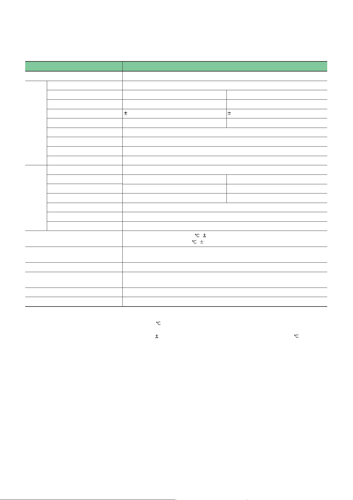
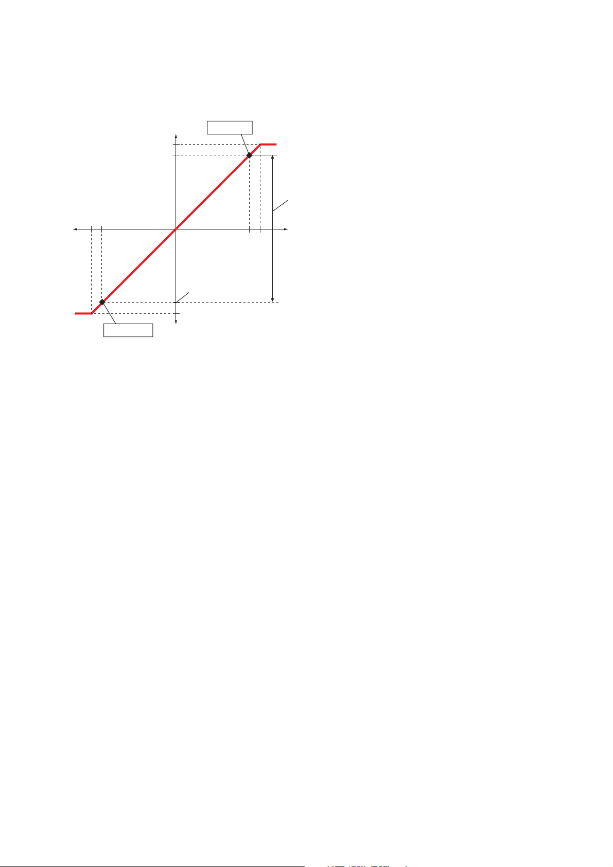
2-3-1 Conversion characteristics of analog voltage input
Output range Digital input range
0 to 5 V 0 to 16000 0 to 10000
1 to 5 V 0 to 16000 0 to 10000
0 to 10 V 0 to 16000 0 to 10000
-10 to 10 V -8000 to 8000 0 to 10000
1) Characteristic curve for the input range of 0 to 5 V
Digital output value
(INT type)
Gain value
(10250) 16400
(10000) 16000
(Note)
Practicable digital
output range
Offset value
-0.125
0
-400 (-250)
5 5.125
Analog input voltage (V)
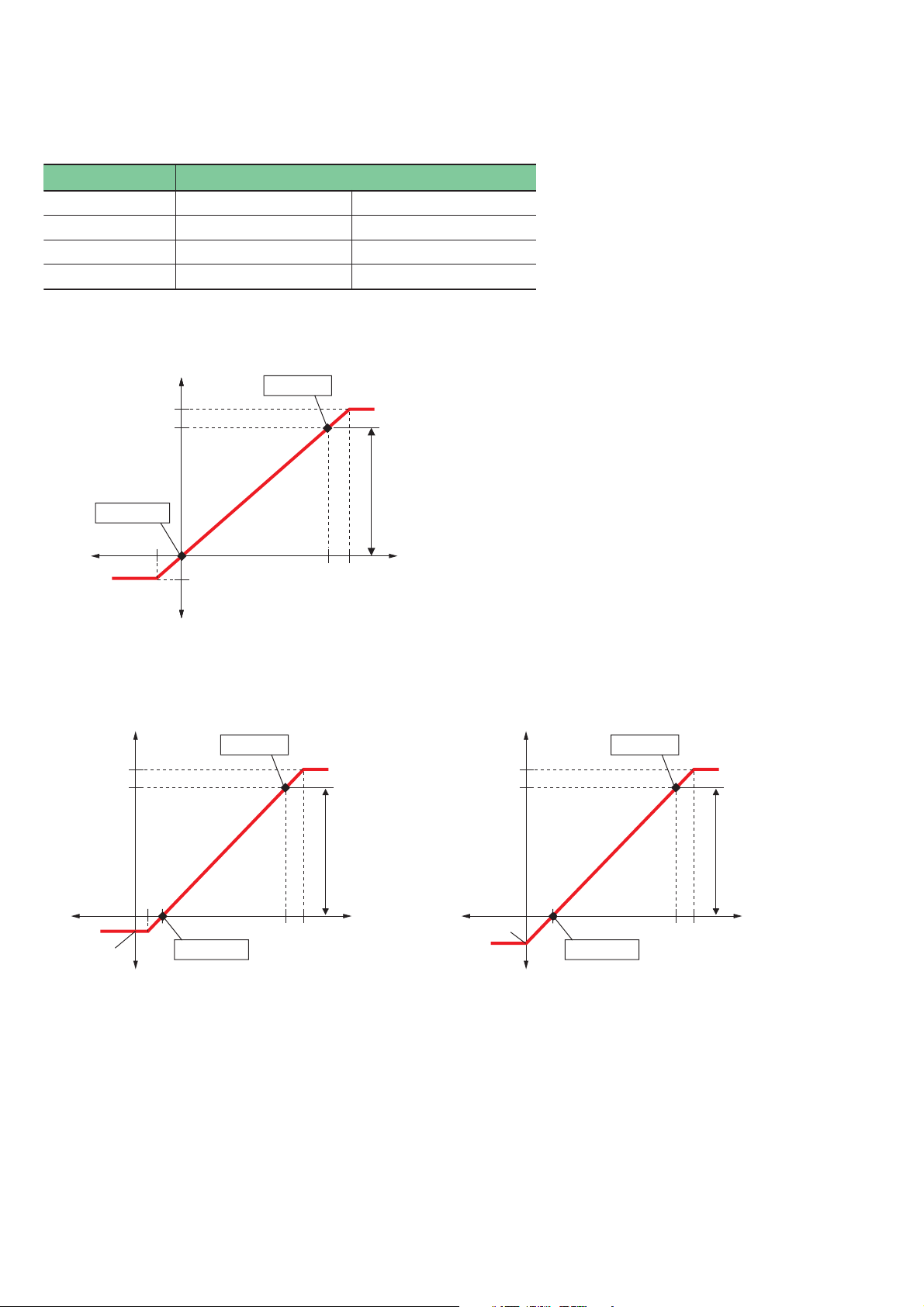
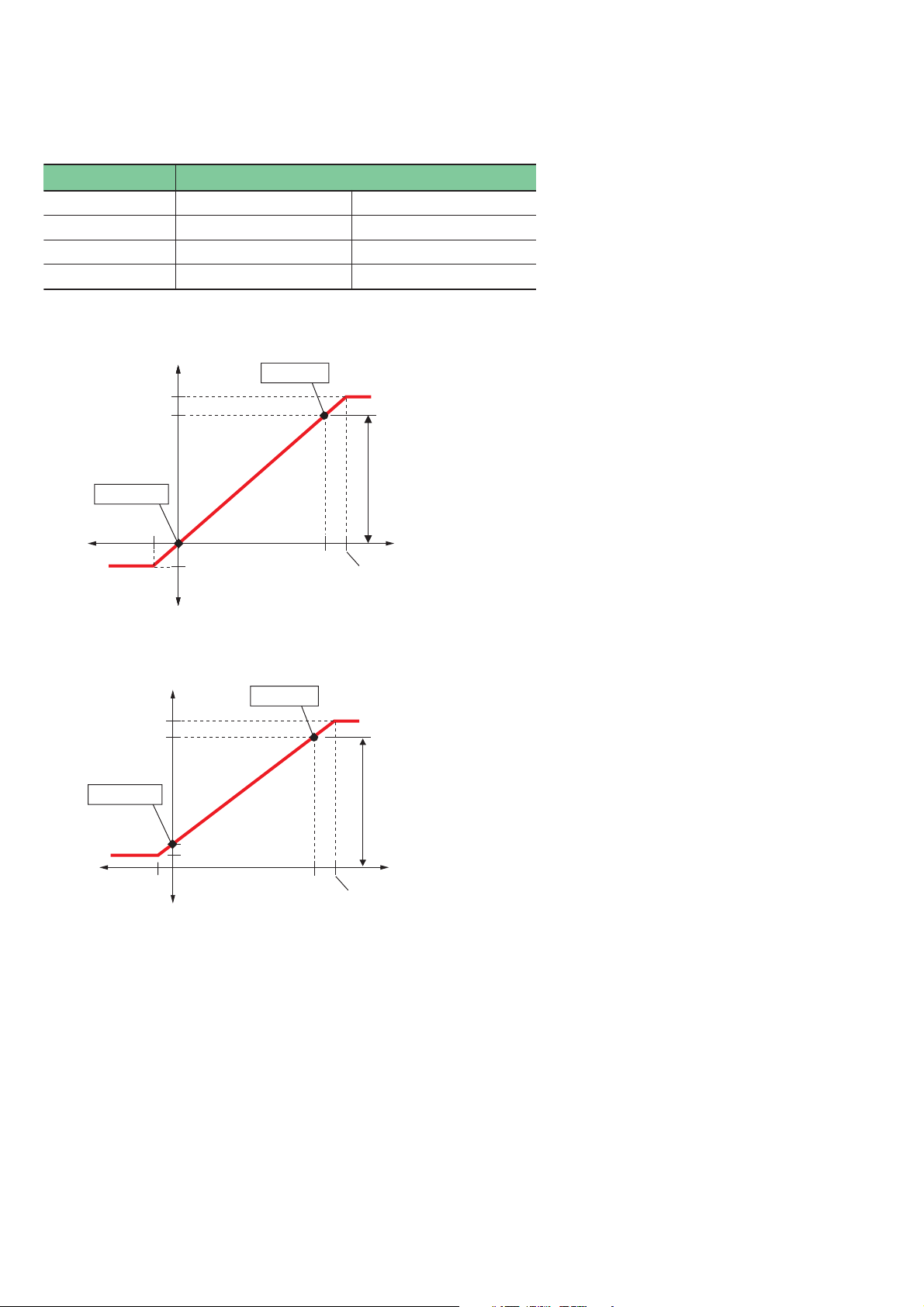
2) Characteristic curve for the input range of 1 to 5 V
Digital output value
(INT type)
Gain value
(10250) 16400
(10000) 16000
(Note)
Practicable digital
output range
(-250) -400
0.9
0
1
Offset value
5 5.1
Analog input
voltage (V)
<NP1AWH6-MR only>
Digital output value
(INT type)
16400
16000
0
-4000
1
Offset value
Gain value
5 5.1
Practicable digital
output range
Analog input
voltage (V)
Note: Parenthesized figures mean the values when the unit of digital output value is % in Fixed Range Operation mode (excl.
NP1AWH6-MR). In software Set Range Operation mode, scaling is necessary to express output values by the %.
2-6
Page 15
Section 2 Specifications
2-3 Conversion Characteristics
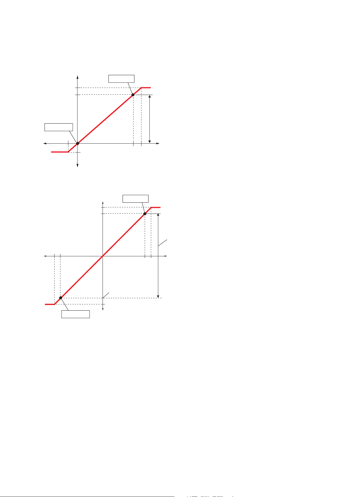
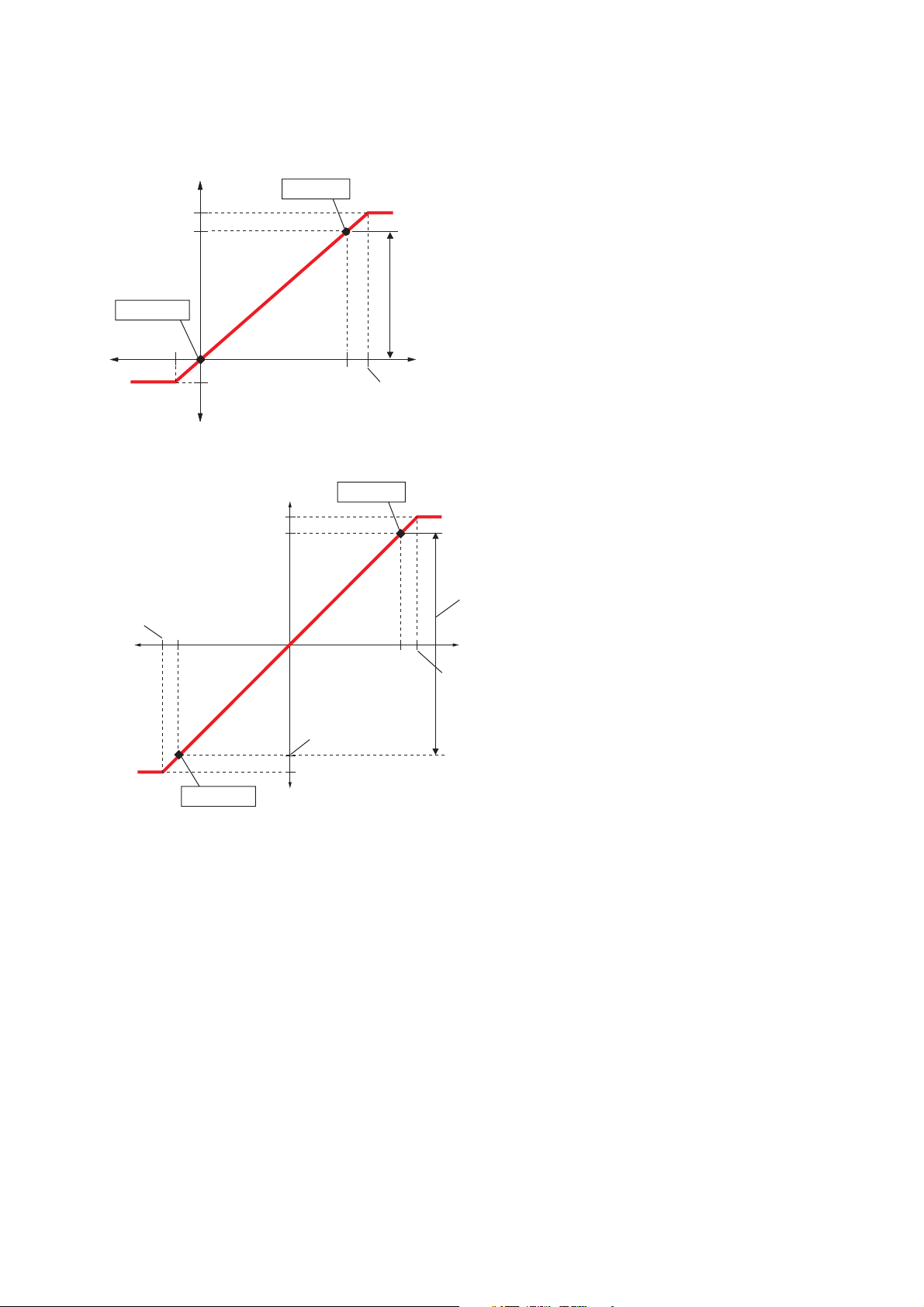
3) Characteristic curve for the input range of 0 to 10 V
Digital output value
(INT type)
Gain value
(10250) 16400
(10000) 16000
(Note)
Practicable digital
output range
Offset value
-0.25
0
-400 (-250)
10 10.25
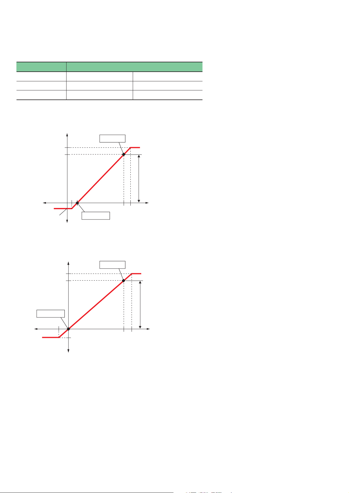
4) Characteristic curve for the input range of -10 to 10 V
Digital output value
(INT type)
(10125) 8200
(10000) 8000
(Note)
Gain value
Analog input voltage (V)
Practicable digital
output range
-10.25 -10
Offset value
0
-8000 (0)
-8200 (-125)
10 10.25
Analog input voltage (V)
Note: Parenthesized figures mean the values when the unit of digital output value is % in Fixed Range Operation mode (excl.
NP1AWH6-MR). In software Set Range Operation mode, scaling is necessary to express output values by the %.
2-7
Page 16
Section 2 Specifications
2-3 Conversion Characteristics
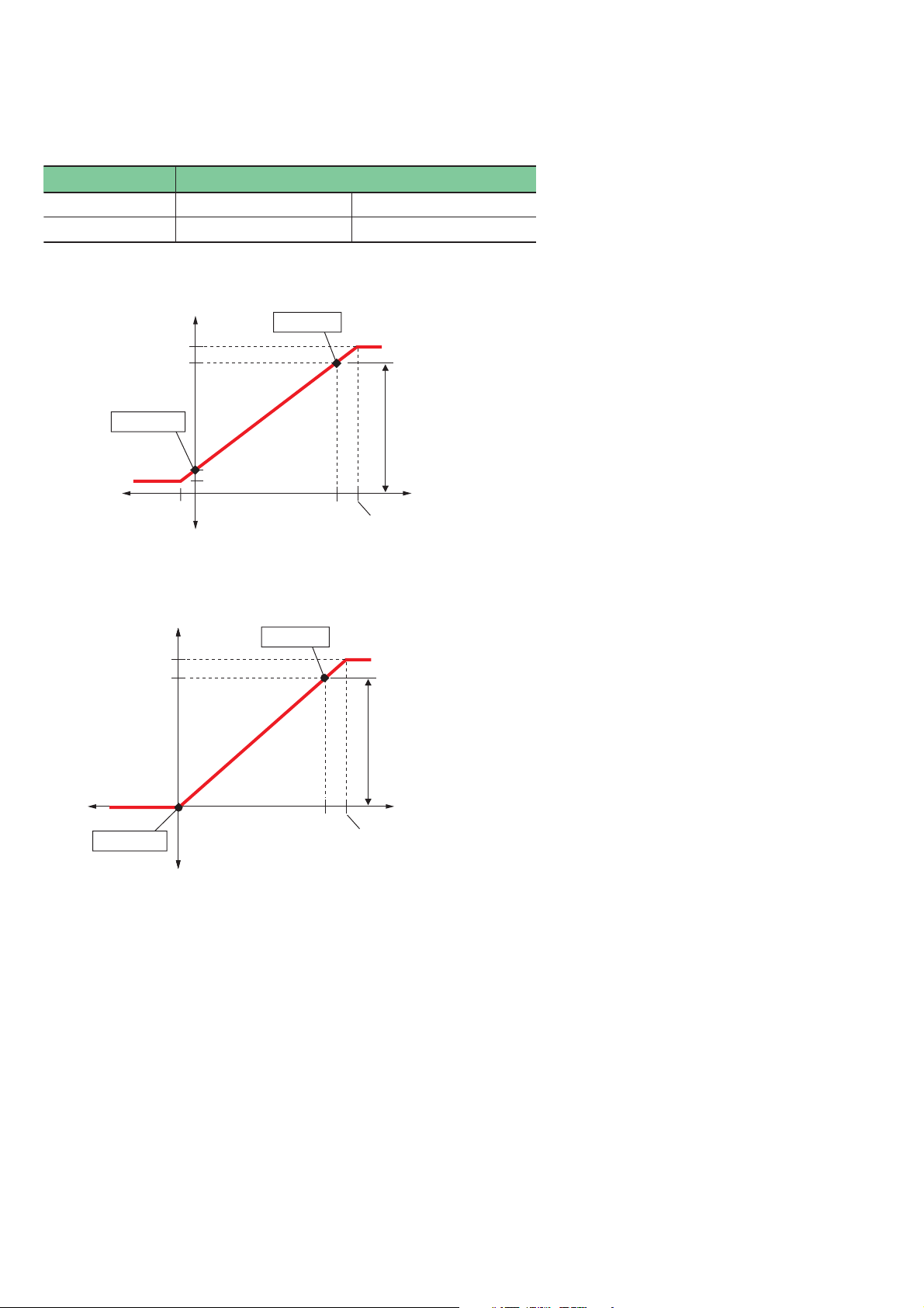
2-3-2 Conversion characteristics of analog current input
Input range Digitaloutput range
4 to 20 mA 0 to 16000 0 to 10000
0 to 20 mA 0 to 16000 0 to 10000
-20 to 20 mA -8000 to 8000 0 to 10000
1) Characteristic curve for the input range of 4 to 20 mA
Digital output value
(INT type)
Gain value
(10250) 16400
(10000) 16000
(Note)
Practicable digital
output range
3.6
(-250) -400
0
4
Offset value
20 20.4
Analog input current (mA)
2) Characteristic curve for the input range of 0 to 20 mA
Digital output value
(INT type)
Gain value
(10250) 16400
(10000) 16000
(Note)
Practicable digital
output range
Offset value
-0.5
0
-400 (-250)
20 20.5
Note: Parenthesized figures mean the values when the unit of digital output value is % in Fixed Range Operation mode (excl.
NP1AWH6-MR). In software Set Range Operation mode, scaling is necessary to express output values by the %.
Analog input current (mA)
2-8
Page 17
Section 2 Specifications
2-3 Conversion Characteristics
3) Characteristic curve for the input range of -20 to 20 mA
Digital output value
-20.5 -20
(INT type)
(10125) 8200
(10000) 8000
(Note)
0
Offset value
Gain value
Practicable digital
output range
Analog input current (mA)
20 20.5
-8000 (0)
-8200 (-125)
Note: Parenthesized figures mean the values when the unit of digital output value is % in Fixed Range Operation mode (excl.
NP1AWH6-MR). In software Set Range Operation mode, scaling is necessary to express output values by the %.
2-9
Page 18
Section 2 Specifications
2-3 Conversion Characteristics
2-3-3 Conversion characteristics of analog voltag output
Output range Digital input range
0 to 5 V 0 to 16000 0 to 10000
1 to 5 V 0 to 16000 0 to 10000
0 to 10 V 0 to 16000 0 to 10000
-10 to 10 V -8000 to 8000 -
1) Characteristic curve for the output range of 0 to 5 V
Analog output voltage (V)
Gain value
5.125
5
(Note)
Offset value
(-250) -400
0
-0.125
16000
(10000)
Practicable analog
output range
Digital input value
(INT type)
16400
(10250)
2) Characteristic curve for the output range of 1 to 5 V
Analog output voltage (V)
Gain value
5.1
5
Offset value
(-250) -400
1
-0.9
0
(Note)
16000
(10000)
Practicable analog
output range
Digital input value
(INT type)
16400
(10250)
Note 1: Parenthesized figures mean the values when the unit of digital input value is % in Fixed Range Operation mode (excl.
NP1AWH6-MR). In Software Set Range Operation mode, scaling is necessary to express input values by the %.
Note 2: If parameter mode is activated in Software Set Range Operation mode, analog output value becomes equal to the
offset value.
2-10
Page 19
Section 2 Specifications
2-3 Conversion Characteristics
3) Characteristic curve for the output range of 0 to 10 V
Analog output voltage (V)
Gain value
10.25
10
Practicable analog
Offset value
output range
(-250) -400
0
-0.25
(Note)
16000
(10000)
Digital input value
(INT type)
16400
(10250)
4) Characteristic curve for the output range of -10 to 10 V
-8200
(-125)
Analog output voltage (V)
10.25
10
-8000
(Note)
(0)
Offset value
0
-10
-10.25
Gain value
8000
(10000)
Practicable analog
output range
Digital input value
(INT type)
8200
(10125)
Note 1: Parenthesized figures mean the values when the unit of digital input value is % in Fixed Range Operation mode (excl.
NP1AWH6-MR). In Software Set Range Operation mode, scaling is necessary to express input values by the %.
Note 2: For the range of -10 to 10 V, the unit of % cannot be selected by switch setting.
Note 3: If parameter mode is activated in Software Set Range Operation mode, analog output value becomes equal to the
offset value, except that 0 V is output for the range of -10 to 10 V.
2-11
Page 20
Section 2 Specifications
2-3 Conversion Characteristics
2-3-4 Conversion characteristics of analog current output
Output range Digital input range
4 to 20 mA 0 to 16000 0 to 10000
0 to 20 mA 0 to 16000 0 to 10000
1) Characteristic curve for the output range of 4 to 20 mA
Analog output current (mA)
Gain value
20.4
20
Offset value
(Note)
4
(-250) -400
0
-3.6
(Note)
16000
(10000)
Practicable analog
output range
Digital input value
(INT type)
16400
(10250)
2) Characteristic curve for the output range of 0 to 20 mA
Analog output current (mA)
Gain value
20.5
20
Practicable analog
output range
Offset value
0
16000
(10000)
(Note)
Digital input value
(INT type)
16400
(10250)
Note 1: Parenthesized figures mean the values when the unit of digital input value is % in Fixed Range Operation mode (excl.
NP1AWH6-MR). In Software Set Range Operation mode, scaling is necessary to express input values by the %.
Note 2: If parameter mode is activated in Software Set Range Operation mode, analog output value becomes equal to the
offset value.
2-12
Page 21

Section 2 Specifications
2-4 Functional Specifications
2-4-1 Analog input module functions
(1) Switch batch setting function
With the operation setting switches provided on the module rear panel, it is possible to set the following items for all the
channels in a batch:
Operation range and the unit for digital conversion
Moving average execution times (can be selected from 1, 2, 4 and 8 times).
When the unit of digital output value is set to %, the module operates, regarding
Lower limit value of range as 0.00%,
Upper limit value of range as 100.00%, and
Digital output range as -2.50% to 102.5%.
Note 1: If the Switch Batch Setting function is enabled after scaling values or other parameters have been changed from the
parameter setting window, the changed parameters are not reflected on operation and the parameters return to the
default values.
Note 2: When the switch is set to an invalid value, the status code of “30005” is returned to all the channels.
Note 3: The setting of the switch cannot be checked from application program. Be sure to check the switch setting before the
system is started or before maintenance or replacement is performed.
DD
D For how to set the switch, refer to “2-5 Names and Functions”.
DD
(2) Individual channel operation range setting function
When the operation setting switch on the module rear panel is set to “Software Set Range”, operation range can be set for
individual channel by application program.
(3) Individual channel moving average execution times setting function
When the operation setting switch on the module rear panel is set to “Software Set Range”, moving average execution times
can be set for individual channel by application program. Default is once (sampling operation). Averaging execution times can
be selected from 1, 2, 4 and 8.
Note: The “Average” switch on the module rear panel is disabled.
(4) Individual channel conversion enable/disable setting function
When the operation setting switch on the module rear panel is set to “Software Set Range”, enable/disable of A/D conversion
can be set for individual channel by application program. Default is “enable conversion”.
Sampling time can be reduced by disabling A/D conversion for unused channels. For conversion disabled channels, digital
output value is fixed to 0 (zero).
(5) Individual channel gain/offset value fine adjustment function
When the operation setting switch on the module rear panel is set to “Software Set Range”, gain and offset values can finely
be adjusted for individual channel by application program.
* For the detailed specifications and setting, refer to “4-1-2 (6)”.
(6) Scaling function
When the operation setting switch on the module rear panel is set to “Software Set Range”, the scale for A/D conversion can
be set for individual channel by application program.
* For the detailed specifications and setting, refer to “4-1-2 (6)”.
2-13
Page 22

Section 2 Specifications
2-4 Functional Specifications
2-4-2 Analog output module functions
(1) Switch batch setting function
With the operation setting switches provided on the module rear panel, it is possible to set operation range and the unit for
digital input value.
When the unit of digital input value is set to %, the module operates, regarding
Lower limit value of range: 0.00%,
Upper limit value of range: 100.00%
Digital output range: -2.50% to 102.5%.
Note 1: If the Switch Batch Setting function is enabled after scaling values or other parameter have been changed from the
parameter setting window, the changed parameters are not reflected on operation and the parameters return to the
default values.
Note 2: When the switch is set to an invalid value, bit 11 of offset address +0 is set ON.
Note 3: The setting of the switch cannot be checked from application program. Be sure to check the switch setting before the
system is started or before maintenance or replacement is performed.
DD
DFor how to set the switch, refer to “2-5 Names and Functions”.
DD
(2) Individual channel operation range setting function
When the operation setting switch on the module rear panel is set to “Software Set Range”, operation range can be set for
individual channel by application program.
(3) Output enable/disable setting function (analog 8ch output modules only)
When the operation setting switch on the module rear panel is set to “Software Set Range”, “enable output for all channels” or
“enable output for CH1 to CH4, disable output for CH5 to CH8” can be set by application program.
When “enable output for CH1 to CH4, disable output for CH5 to CH8” is set, sampling time is halved, and the output disabled
channels output 0 V or 0 mA.
Note: Because the accuracy of output value is not guaranteed for output disabled channels, these channels may output
slightly offset values.
(4) Individual channel gain/offset value fine adjustment function
When the operation setting switch on the module rear panel is set to “Software Set Range”, gain and offset values can finely
be adjusted for individual channel by application program.
* For the detailed specifications and setting, refer to “4-2-2 (8)”.
(5) Scaling function
When the operation setting switch on the module rear panel is set to “Software Set Range”, the scale for A/D conversion can
be set for individual channel by application program.
* For the detailed specifications and setting, refer to “4-2-2 (8)”.
When the system is started up, the analog value that corresponds to digital value “0” (zero) is output (for
approximately several hundreds milliseconds since the “ONL” LED has lit till the application program starts).
Therefore, for scaling, the value that corresponds to digital value “0” (zero) should be set such that fail safe
operation will be performed. Also when the system is shut down or becomes abnormal, the analog value that
corresponds to digital value "0" (zero) is output (when this module in I/O Reset mode).
2-14
Page 23

Section 2 Specifications
2-4 Functional Specifications
2-4-3 Analog input/output module functions
(1) Switch batch setting function
With the operation setting switches provided on the module rear panel, it is possible to set operation range.
For analog input, it can be set for 4 channels in a batch; for analog output, 2 channels in a batch.
Note 1: If the Switch Batch Setting function is enabled after scaling values or other parameter have been changed from the
parameter setting window, the changed parameters are not reflected on operation and the parameters return to the
default values.
Note 2: When the switch is set to an invalid value, the status code of “30005” is returned to all the channels.
Note 3: The setting of the switch cannot be checked from application program. Be sure to check the switch setting before the
system is started or before maintenance or replacement is performed.
DD
DFor how to set the switch, refer to “2-5 Names and Functions”.
DD
(2) Individual channel operation range setting function
When the operation setting switch on the module rear panel is set to “Software Set Range”, operation range can be set for
individual channel by application program.
(3) Individual channel moving average execution times setting function
When the operation setting switch on the module rear panel is set to “Software Set Range”, moving average execution times
can be set for individual channel by application program. Default is once (sampling operation). Averaging execution times can
be selected from 1, 2, 4 and 8.
(4) Individual channel conversion enable/disable setting function
When the operation setting switch on the module rear panel is set to “Software Set Range”, enable/disable of A/D conversion
can be set for individual channel by application program. Default is “enable conversion”.
Sampling time can be reduced by disabling A/D conversion for unused channels. For conversion disabled channels, digital
output value is fixed to 0 (zero).
(5) Individual channel gain/offset value fine adjustment function
When the operation setting switch on the module rear panel is set to “Software Set Range”, gain and offset values can finely
be adjusted for individual channel by application program.
* For the detailed specifications and setting, refer to “4-3-2 (8)”.
(6) Scaling function
When the operation setting switch on the module rear panel is set to “Software Set Range”, the scale for A/D conversion can
be set for individual channel by application program.
* For the detailed specifications and setting, refer to “4-3-2 (8)”.
2-15
Page 24
Section 2 Specifications
2-5 Names and Functions
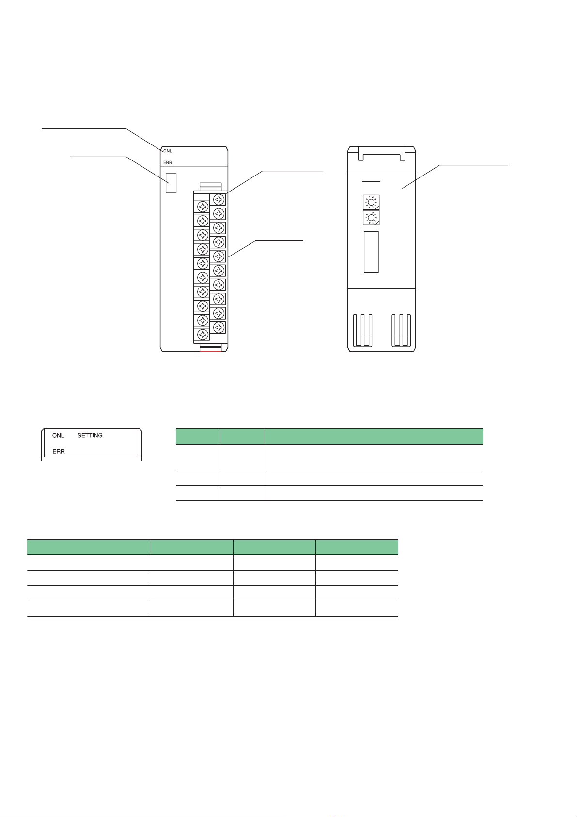
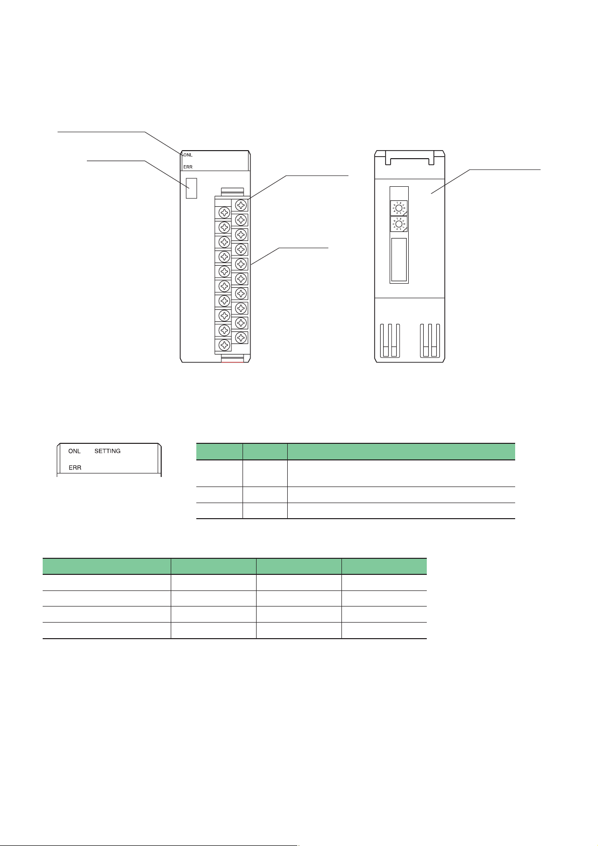
2-5-1 Analog input module (NP1AXH8V-MR/NP1AXH8I-MR)
(1) Names
1) Status indication LED
4) Version seal
Front Rear
(2) Functions
1) Status Indication LED
Indicates the current status of the analog input module.
3) Detachable
terminal block
Specification
name plate
2) Operation setting
switches
Symbol Color Description
ONL Green Lights when the module is operating normally. Blinks
whileconnectingtoSXbus.
ERR Red Lights whenthe module is abnormal.
SETTING Green Blinks while gain or offset value is being adjusted.
<Example of status indication>
O: Li ghting, U: Blinking, -: Unlit
Status ONL (green) ERR (red) SETTING (green)
Initializing
Normally operating O - Adjusting offset/gainvalue O Fatalfault - O -
U
--
U
2-16
Page 25
Section 2 Specifications
2-5 Names and Functions
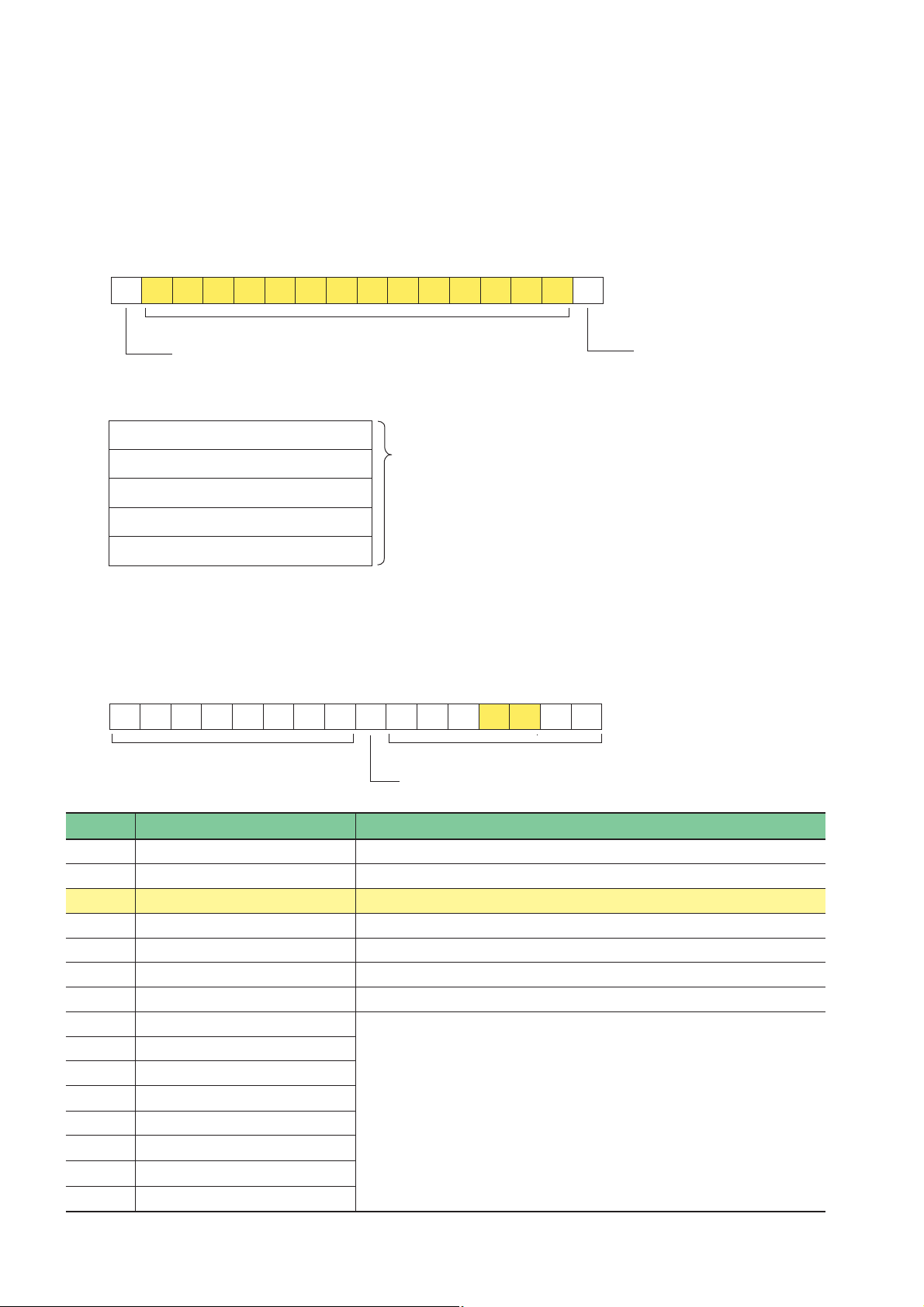
2) Operation setting switches
These switches are used to set input range and moving average execution times.
“Average” switch: Used to set a same value of moving average execution times for all channels. In Software Set Range
Operation mode, the setting of this switch is ignored, and instead the initial value is used for operation.
For more information, refer to “Section 4 Software Interface”.
“Range” switch: When this switch is set to one of numbers “0” to “7”, same range is set for all channels. It is impossible to
set input range differently for individual channels.
When this switch is set to “8”, Software Set Range Operation mode is activated, and it becomes possible
to set various parameters differently for individual channels. For more information, refer to “Section 4
Software Interface”.
8
7
9
6
0
5
1
4
2
3
I At shipment, both “Average” and “Range” switches are set to “0” (zero).
8
7
9
6
0
5
1
4
2
3
<Range switch setting list>
Switch No.
0
At shipment
NP1AXH8V-MR
Input range
Digital output
range
Switch No.
-10 to 10 V -8000 to 8000 0
At shipment
NP1AXH8I-MR
Input range
4to20mA
Digital output
range
0 to 16000
1 0 to 10 V 0 to 16000 1 0 to 20 mA
2 0 to 5 V 2 -20 to 20 mA -8000 to 8000
3 1to5V 3 4to20mA
0 to 100004 -10 to 10 V 0 to 10000 4 0 to 20 mA
5 0to10V 5 -20to20mA
6 0 to 5 V 6 Software Set Range Operation mode
7 1to5V 7
8 Software Set Range Operation mode (Note1) 8
Unused (Note 2)
9 Unused (Note 2) 9
<Average switch setting list>
Switch No. NP1AXH8V-MR NP1AXH8I-MR
0
Once (no moving average)
At shipment
1Twice
24times
Note 1:
For how to set in Software Set Range Operation mode,
refer to “Section 4 Software Interface”.
Note 2:
If an unused number is set, a “switch setting error” will
occur.
38times
4 to 9 Unused (no moving average)
3) Detachable terminal block
M3 20-pole detachable terminal block. For terminal arrangement, refer to “5-1-1 Terminal arrangement”. For wiring, be sure to
use crimp type terminals and surely tighten them (tightening torque: 0.5 to 0.7 N-m.)
4) Version seal
Versions of the hardware and firmware of the module are indicated on this seal.
2 0
3 0
Hardware version
Firmware version
2-17
Page 26
Section 2 Specifications
2-5 Names and Functions
2-5-2 Analog output module (NP1AYH8V-MR, NP1A YH8I-MR, NP1AYH4V-MR, NP1AYH4I-MR)
(1 ) Names
<Analog 8ch output module>
1) Status indication LED
4) Version seal
<Analog 4ch output module>
1) Status indication LED
SETTING
ONL
ERR
Front Rear
3) Detachable
terminal block
Specification
name plate
2) Operation setting
switches
4) Version seal
SETTING
ONL
ERR
Front Rear
3) Detachable
terminal block
Specification
name plate
2) Operation setting
switches
2-18
Page 27
Section 2 Specifications
)
2-5 Names and Functions
(2) Functions
1) Status indication LED
Indicates the current status of the analog output module.
Symbol Color Description
ONL Green Lights when the module is operating normally. Blinks
whileconnectingtoSXbus.
ERR Red Lights whenthe module is abnormal.
SETTING Green Blinks while gain or offset value is being adjusted.
<Example of status indication>
O: Li ghting, U: Blinking, -: Unlit
Status ONL (green) ERR (red) SETTING (green)
Initializing
Normally operating O - Adjusting offset/gainvalue O Fatalfault - O -
U
--
U
2) Operation setting switch
Used to set output range.
“Range” switch: When this switch is set to one of numbers “0” to “7” (“0” to “3” for current output modules), same output
range is set for all channels. It is impossible to set output range differently for individual channel.
When this switch is set to “8” (“4” for current output modules), Software Set Range Operation mode is
activated, and it becomes possible to set various parameters differently for individual channel. For more
information, refer to “Section 4 Software Interface”.
8
7
9
6
0
5
4
3
I At shipment, this switch is set to “0” (zero).
1
2
<Range switch setting list>
Switch No.
0
At shipment
NP1AYH8V-MR
Output range
Digital input
range
Switch No.
0 to 10 V 0 to 16000 0
At shipment
NP1AYH8I-MR
Output range
Digital input
range
4 to 20 mA 0 to 16000
1 0to5V 1 0to20mA
2 1 to 5 V 2 4 to 20 mA 0 to 10000
3 -10 to 10 V -8000 to 8000 3 0 to 20 mA
4 0 to 10 V 0 to 10000 4 S oftware Set Range Operation mode
5 0to5V 5
6 1to5V 6
7 Unused (the operationfor switch No. 0) 7
Unused (the operation for switchNo. 0
8 Software Set Range Operation mode (Note) 8
9 Unused (the operationfor switch No. 0) 9
Note: For how to set in Software Set Range Operation mode, refer to "Section 4 Software Interface".
2-19
Page 28

Section 2 Specifications
2-5 Names and Functions
3) Detachable terminal block
M3 20-pole detachable terminal block (M3 10-pole for 4ch output modules). For terminal arrangement, refer to “5-2-1 Terminal
arrangement”. For wiring, be sure to use crimp type terminals and surely tighten them (tightening torque: 0.5 to 0.7 N-m.)
4) Version seal
Versions of the hardware and firmware of the module are indicated on this seal.
2 0
3 0
Hardware version
Firmware version
2-20
Page 29
Section 2 Specifications
2-5 Names and Functions
2-5-3 Analog input/output module (NP1AWH6-MR)
(1 ) Names
1) Status indication LED
4) Version seal
Front Rear
3) Detachable
terminal block
Specification
name plate
(2) Functions
1) Status Indication LED
Indicates the current status of the analog input/output module.
2) Operation setting
switches
Symbol Color Description
ONL Green Lights when the module is operating normally. Blinks
whileconnectingtoSXbus.
ERR Red Lights whenthe module is abnormal.
SETTING Green Blinks while gain or offset value is being adjusted.
<Example of status indication>
O: Li ghting, U: Blinking, -: Unlit
Status ONL (green) ERR (red) SETTING (green)
Initializing
Normally operating O - Adjusting offset/gainvalue O Fatalfault - O -
U
--
U
2-21
Page 30

Section 2 Specifications
2-5 Names and Functions
2) Operation setting switches
These switches are used to set input/output range. When input/output range is set with these switches, the same range is set
for input and output channels. It is impossible to set input range differently for individual channels.
8
7
9
6
0
5
1
4
2
3
8
7
9
6
0
5
1
4
2
3
Switch No. Input range Digital output range Switch No. Output range Digital input range
0
At shipment
1 0to5V 1 0to5V
0to10V
0 to 16000
0
At shipment
0to10V
0 to 16000
2 1to5V 2 1to5V
3 -10 to 10 V -8000 to 8000 3 -10 to 10V -8000 to 8000
40to20mA
5 4 to 20 mA 5 4 to 20 mA
0 to 16000
40to20mA
0 to 16000
6 -20 to 20mA -8000 to 8000 6
7 Software Set Range Operation mode (Note) 7
8 Unused (the operationfor switch No. 0) 8
Unused (the operation for switchNo. 0)
9 Unused (the operationfor switch No. 0) 9
Note: For how to set in Software Set Range Operation mode, refer to "Section 4 Software Interface".
3) Detachable terminal block
M3 20-pole detachable terminal block. For terminal arrangement, refer to “5-3-1 Terminal arrangement”. For wiring, be sure to
use crimp type terminals and surely tighten them (tightening torque: 0.5 to 0.7 N-m.)
4) Version seal
Versions of the hardware and firmware of the module are indicated on this seal.
2 0
Hardware version
3 0
Firmware version
2-22
Page 31

Section 2 Specifications
2-6 Dimensions
(Unit: mm)
35
111
90
105
2-23
Page 32
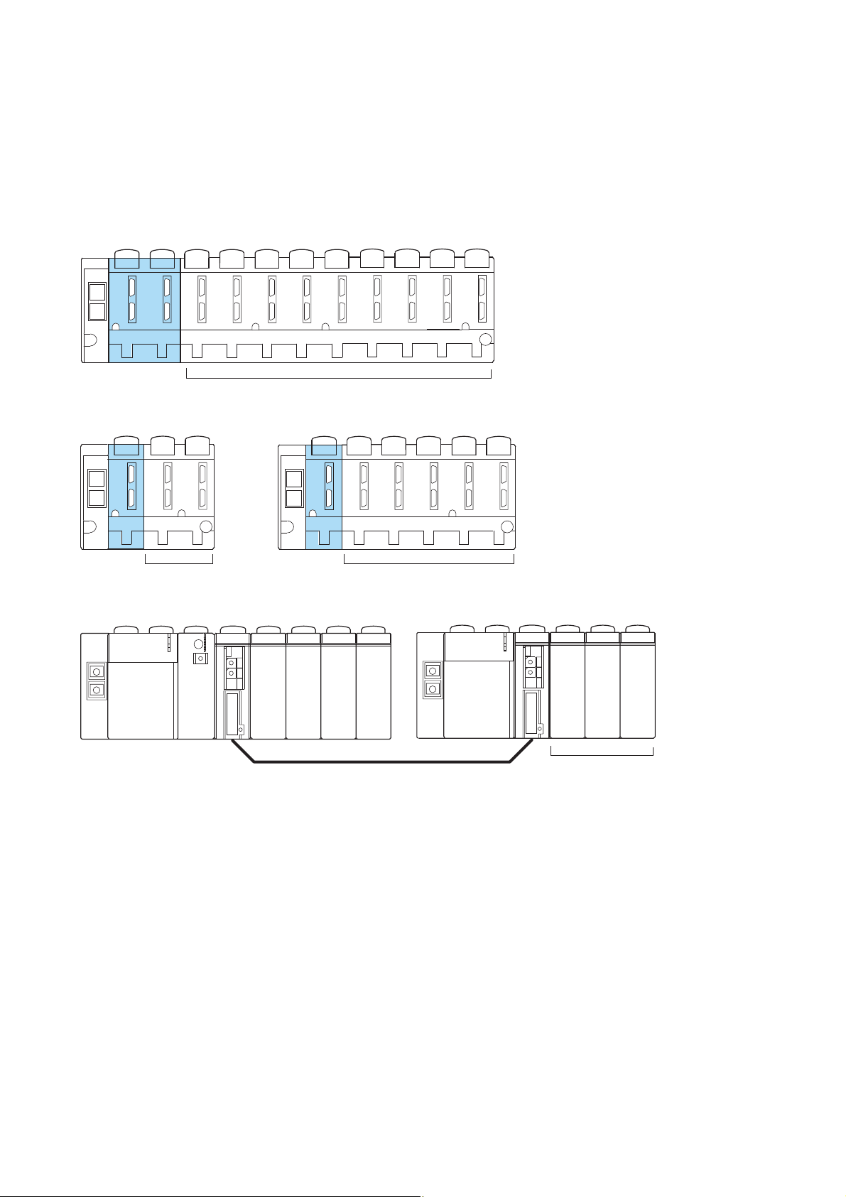
Section 3 System Configuration
3-1 Mounting on the Base Board
3-1-1 Mounting position
To use these modules, they need to be connected to the SX bus of MICREX-SX series SPH or to the link (remote I/O) of I/O
master module. Their mounting position on the base board is as follows.
<8/11/13-slot base board>
These modules can be mounted in any slot except those for the power supply module
(the two slots from the left on the base board).
Mountable slots
<3/6-slot base board>
Mountable slots
Note: These modules can be mounted also on the base board of remote I/O such as T-link,OPCN-1 and DeviceNet.
Mountable slots
Mountable slots
3-1-2 Number of mountable modules
It is possible to connect a maximum of 238 modules to the SX bus (a maximum of 254 modules in one configuration including
the link of the I/O master) (due to hardware limitation). It should be noted, however, that the maximum number of analog
voltage/current input modules and analog voltage/current output modules that can actually be connected is limited by the
number of words (512 words) they occupy in the input/output areas (I/Q areas).
Because the number of words occupied by an analog 8ch module is 12 words and that occupied by an analog 4ch output
module and analog input/output module is 8 words, the maximum number of mountable modules becomes as follows:
Analog 8ch modules: 512 words / 12 words = 42 units
Analog 4ch modules / Analog input/output module: 512 words / 8 words = 64 units
Note: Suppose that 42 units of 8ch analog modules are connected in one configuration, then the input/output areas that other
input/output modules can use become 8 words.
3-1
Page 33
Section 4 Software Interface
4-1 Analog Input Module
NP1AXH8V-MR (voltage input module) and NP1AXH8I-MR (current input module) occupy 12 words of I/O area (input: 8 words,
output: 4 words).
4-1-1 Memory allocation in Switch Batch Setting mode
Moving average execution times for conversion operation is set with the “Average” switch (upper side switch on the module
rear panel), and operation range is set with the “Range” switch (lower side switch on the module rear panel).
Offset
address
15(F)
+0
Channel1 Digitaloutputvalue/Status
+1
Channel 2 Digital output value / Status
+2
Channel 3 Digital output value / Status
+3
Channel4 Digitaloutputvalue/Status
+4
Channel 5 Digital output value / Status
+5
Channel 6 Digital output value / Status
+6
Channel 7 Digital output value / Status
0
This module to CPU module
+7
Channel 8 Digital output value / Status
+8
+9
+10
+11
<Status list>
Status code Error Description
30002
(7532h)
30003
(7533h)
30004
(7534h)
30005
(7535h)
30006
(7536h)
Unused (fixed to 0 (zero))
Unused (fixed to 0 (zero))
Unused (fixed to 0 (zero))
Unused (fixed to 0 (zero))
EEPROM calibrationdata
error (Module fatal fault)
EEPROM user setting data
error
Internal power supplydown
Switch setting error
Conversion error
If the calibration data ofEEPROM is destroyed or if EEPROM cannot be
writtenor read, this erroris notified. Module internalEEPROM is abnormal.
If this error occurred, it is necessary to replace the module.
If the usersetting data of EEPROM is destroyed,this erroris notified.
If this error occurred, allparameters need to be reset. If this error recurs
evenafter parameters are reset, the module seems to have failed.
If the internal power supply of the module becomes down, this error is
notified.
If the operation setti ng switchon the module rear panel is set at invalid
position,this error is notified.
If conversion became abnormalbecause the module failed or was used in an
out-of-spec environment, this erroris notified.
CPU module to this module
Ordinarily digital output values (INT type) are stored in the registers explained above. If the module becomes
abnormal, the following status code (INT type) is stored in these registers. When making an application program,
be sure to interlock erroneous and normal (A/D conversion) conditions.
4-1
Page 34
Section 4 Software Interface
4-1 Analog Input Module
4-1-2 Memory allocation in Software Set Range Operation mode
In Software Set Range Operation mode, memory allocation differs between when operating in A/D conversion mode (during
normal operation) and when operating in parameter mode.
<When operating in A/D conversion mode>
When operating in A/D conversion mode, memory allocation becomes as follows:
Offset
address
15(F)
+0
Channel1 Digitaloutputvalue/Status
+1
Channel 2 Digital output value / Status
+2
Channel 3 Digital output value / Status
+3
Channel4 Digitaloutputvalue/Status
+4
Channel 5 Digital output value / Status
+5
Channel 6 Digital output value / Status
+6
Channel 7 Digital output value / Status
0
This module to CPU module
+7
Channel 8 Digital output value / Status
+8
+9
+10
+11
<When operating in parameter mode>
Parameter mode is activated when bit 7 of the parameter type setting register is set ON. In parameter mode, memory
allocation becomes as follows:
Offset
address
15(F)
+0
+1
+2
+3
+4
+5
Unused (fixed to 0 (zero))
Unused (fixed to 0 (zero))
Unused (fixed to 0 (zero))
Unused (fixed to 0 (zero))
Module status
Parameter typ e setting status
Parameter read data
CPU module to this module
0
This module to CPU module
+6
+7
+8
+9
+10
+11
Parameter type setting
CPU module to this module
Parameter setting data
4-2
Page 35
Section 4 Software Interface
4-1 Analog Input Module
(1 ) Digital output value/status register (offset address: +0 to +7)
When this module is in A/D conversion mode, digital output values and/or statuses are stored in the registers of offset
address +0 to +7.
* When using D300win, assign INT type variables to these registers.
Offset
address
15(F)
+0
Channel1 Digitaloutputvalue/Status
+1
Channel 2 Digital output value / Status
+2
Channel 3 Digital output value / Status
+3
Channel4 Digitaloutputvalue/Status
+4
Channel 5 Digital output value / Status
+5
Channel 6 Digital output value / Status
+6
Channel 7 Digital output value / Status
+7
Channel 8 Digital output value / Status
0
<Status list>
Status code C ondition of modul Descriptio n
30001
(7531h)
30002
(7532h)
30003
(7533h)
30004
(7534h)
30005
(7535h)
30006
(7536h)
Parameter mode Parameters are now being set or read out.
EEPROM calibrationdata
error
(Module fatalfault)
EEPROM user setting data
error
Internal power supplydown
Switch setting error
Conversion error
Ordinarily digital output values (INT type) are stored in the registers explained above. If the module becomes
abnormal, the following status code (INT type) is stored in these registers. When making an application program,
be sure to interlock erroneous and normal (A/D conversion) conditions.
If the calibration data ofEEPROM is destroyed or if EEPROMcannot be
writtenor read, this erroris notified. Module internalEEPROM is abnormal.
If this error occurred, it is necessary to replace the module.
If the usersetting data of EEPROM is destroyed,this erroris notified.
If this error occurred, allparameters need to be reset. If this error recurs
evenafter parameters are reset, the module seems to have failed.
If the internal power supply of the module becomes down, this error is
notified.
If the operation setti ng switchon the module rear panel is set at invalid
position,this error is notified.
If conversion became abnormalbecause the module failed or was used in an
out-of-spec environment, this erroris notified.
(2 ) Module status register (offset address +0)
When the module is in parameter mode, offset address +0 becomes the “module status register”, in which the code “30001”
(INT type) is stored, indicating that the parameter mode (parameters are now being set or read out) is activated.
* When using D300win, assign an INT type variable to this register.
+0
30001(7531h)
4-3
Page 36
Section 4 Software Interface
4-1 Analog Input Module
(3 ) Parameter type setting status register (offset address +1)
This register stores the information of what parameter is now being written or read by the module.
* When using D300win, assign a WORD type variable to this register. If you access by the bit, assign a BOOL type variable to
each bit.
15(F) 078
+1
Channel No. Parameter type
Bit Flag name Description
0 Operation parameter read mode ON: Operation parameter read mode (allchannels in a batch)
1 Scaling parameterread mode ON: Scaling parameter read mode (individual channel)
2, 3 Unused
4 Operation parameter write mode ON: Operation parameter write mode (all channels in a batch)
5 Scaling parameter write mode ON:Scaling parameter write mode (individual channel)
6 Offset/gain adjustment mode ON: Offset/gainadjustmentmode (indivi dual channel)
7 Unused
8 Channel 1 In "scaling parameter read mode", "scaling parameter write mode" or
9 Channel 2
10(A) Channel 3
11(B) Channel 4
12(C) Channel 5
13(D) Channel 6
14(E) Channel 7
15(F) Channel 8
"offset/gain adjustment mode", one of bits 8 to 15 is set ON to indicate
whi ch channel is nowbeing set or read out.
(4) Parameter read data register (offset address +2 to +7)
In “operation parameter read mode”, “scaling parameter read mode” or “offset/gain adjustment mode”, the content of the
setting for the corresponding mode is stored in this register.
1) When operation parameter read mode is activated
When parameter mode (module status register = 30001(7531h)) is activated and bit 0 of the parameter type setting status
register is set ON, the status of the operation parameter is stored.
* When using D300win, assign WORD type variables to these registers.
15(F) 0
+2
+3
+4
+5 to +7
Conversion enable/disable
Input range
Moving average execution times
Unused (fixed to 0 (zero))
Unused (fixed to 0 (zero))
4-4
Page 37

Section 4 Software Interface
f
4-1 Analog Input Module
<Conversion enable/disable, the unit of digital output value> (offset address +2)
Bit Flag name Descriptio n
0to7 Unused
8 Channel 1 Conversion enable/disable OFF: Enable,
9 Channel 2 Conversion enable/disable
10 C hannel 3 C onversion enable/disable
11 Channel 4 Conversion enable/disable
12 C hannel 5 C onversion enable/disable
13 C hannel 6 C onversion enable/disable
14 C hannel 7 C onversion enable/disable
15 C hannel 8 C onversion enable/disable
<Input range setting> (Offset address +3)
ON: Disable
Bit Flag name
0(L)
1(H)
2(L)
3(H)
4(L)
5(H)
6(L)
7(H)
8(L)
9(H)
10 (L)
11 (H)
12 (L)
13 (H)
14 (L)
15 (H)
Channel 1 Input range
Channel 2 Input range
Channel 3 Input range
Channel 4 Input range
Channel 5 Input range
Channel 6 Input range
Channel 7 Input range
Channel 8 Input range
Descriptio n
ThesetrangeisindictedbyacombinationofON/OFFstatuso
two bits.
<NP1AXH8V-MR>
H L
OFF OFF : -10 to 10 V
OFF ON : 0 to 10 V
ON OFF : 0 to 5 V
ON ON : 1 to 5 V
<NP1AXH8I-MR>
H L
OFF OFF : 4 to 20 mA
OFF ON : 0 to 20 mA
ON OFF : -20 to 20 mA
ON ON : 4 to 20 mA
4-5
Page 38

Section 4 Software Interface
4-1 Analog Input Module
<Moving average execution times setting> (offset address +4)
Bit Flag name
0(L)
1(H)
2(L)
3(H)
4(L)
5(H)
6(L)
7(H)
8(L)
9(H)
10 (L)
11 (H)
12 (L)
13 (H)
14 (L)
15 (H)
Channel 1
Moving average execution times
Channel 2
Moving average execution times
Channel 3
Moving average execution times
Channel 4
Moving average execution times
Channel 5
Moving average execution times
Channel 6
Moving average execution times
Channel 7
Moving average execution times
Channel 8
Moving average execution times
Descriptio n
Moving average execution times is indicted by a combination
of ON/OFF status of two bits.
H L
OFF OFF : Once
OFF ON : Twice
ON OFF : 4 times
ON ON : 8 times
2) When scaling parameter read mode is activated
When parameter mode is activated (module status register = 30001) and bit 1 of the parameter type setting status register is
set ON, the scaling parameter setting status of the corresponding channel is stored.
* When using D300win, assign INT type variables to these registers.
15(F) 0
+2
+3
+4 to 7
Offset value
Gain value
Unused (fixed to 0 (zero))
4-6
Page 39
Section 4 Software Interface
4-1 Analog Input Module
3) When offset/gain adjustment mode is activated
When parameter mode is activated (module status register = 30001(7531h)) and bit 6 of the parameter type setting status
register is set ON, the status of offset/gain adjustment is indicated. For this, the digital output values of the 5 channels starting
with specified channel, EEPROM writing completion flag, and offset/gain value indication flag are displayed.
* When using D300win, assign an WORD type variable to this register (offset address+2). If you access by the bit, assign
a BOOL type variable to each bit.
15(F) 08
+2
Unused (fixed to 0 (zero))
OFF: Offset value is displayed.
ON: Gain value is displayed.
15 0
ON: Module internal EEPROM
writing completed.
+3
+4
+5
+6
+7
Channel n Digital output value
Channel n+1 Digital output value
Channel n+2 Digital output value
Channel n+3 Digital output value
Channel n+4 Digital output value
Parameter setting data (INT type)
(The data for 5 channels starting with the first channel
that is specified by offset address +9 is displayed.)
* When using D300win, assign INT type variables to
these registers.
(5) Parameter type setting register (Offset address +8)
Parameter type and channel number for reading/writing parameters are set in this register.
* When using D300win, assign a WORD type variable to this register. If you access by the bit, assign a BOOL type variable to
each bit.
15(F) 078
+8
Channel No.
Bit Flag name Description
0 Operation parameter read mode ON: Operation parameter read mode (allchannels in a batch)
1 Scaling parameterread mode ON: Scaling parameter read mode (individual channel)
2, 3 Unused
4 Operation parameter write mode ON: Operation parameter write mode (all channels in a batch)
5 Scaling parameter write mode ON:Scaling parameter write mode (individual channel)
6 Offset/gain adjustment mode ON: Offset/gainadjustmentmode (indivi dual channel)
7 Parameter mode ON: Parameter mode, OFF: A/D conversion mode
8 Channel 1 In "scaling parameter read mode", "scaling parameter write mode" or
9 Channel 2
10 Channel 3
11 Channel 4
12 Channel 5
13 Channel 6
14 Channel 7
15 Channel 8
"offset/gain adjustment mode", arbitrarychannel i s specified. In "scaling
parameter read mode", one of bits 8 to 15 is set ON to specify a channel
for whichparameters are to be set. When same data is to be set in
"scaling parameter write mode" or "offset/gain adjustment mode", multiple
arbitrary channels may be specified.
Parameter type
Request to set parameter
4-7
Page 40
Section 4 Software Interface
A
4-1 Analog Input Module
(6) Parameter setting data register (offset address +9 to +1 1)
When bit 7 of the parameter type setting register (offset address +8) is set ON, module status (offset address +0) becomes
“30001” (INT type) and “parameter mode” is activated.
The set values of “operation parameter write” mode, “scaling parameter” mode or “offset/gain adjustment” mode are written in
this register.
1) When operation parameter write mode is activated
In this mode, data is set in the locations as shown below, and “operation parameter write mode flag” (bit 4 of the parameter
type setting register) is set ON.
* When using D300win, assign WORD type variables to these registers. If you access by the bit, assign a BOOL type variable
to each bit.
15(F) 0
+9
+10(A)
+11(B)
<Conversion enable/disable> (offset address +9)
Bit Flag name Descriptio n
0to7 Unused
8 C hannel 1 Conversion enable/disable Conversion is enabled or di sabled whenthe corresponding bit
9 C hannel 2 Conversion enable/disable
10 Channel 3 Conversion enable/disable
11 Channel 4 Conversion enable/disable
12 Channel 5 Conversion enable/disable
13 Channel 6 Conversion enable/disable
14 Channel 7 Conversion enable/disable
15 Channel 8 Conversion enable/disable
<Input range> (offset address +10)
Bit Flag name
0(L),1(H)
2(L),3(H)
4(L),5(H)
6(L),7(H)
8(L),9(H)
10 (L), 11 (H)
12 (L), 13 (H)
14 (L), 15 (H)
Conversion enable/disable
Input range
Moving average execution times
Channel 1 Input range Range is set by a combination of ON/OFF status of two bits.
Channel 2 Input range
Channel 3 Input range
Channel 4 Input range
Channel 5 Input range
Channel 6 Input range
Channel 7 Input range
Channel 8 Input range
Unused (fixed to 0 (zero))
is setto OFF orON.
OFF: E nable,
ON: Disable
Descriptio n
<NP1AXH8V-MR>
H L
OFF OFF : -10 to 10 V
OFF ON : 0 to 10 V
ON OFF : 0 to 5 V
ON ON : 1 to 5 V
<NP1AXH8I-MR>
H L
OFF OFF : 4 to 20 mA
OFF ON : 0 to 20 mA
ON OFF : -20 to 20 m
ON ON : 4 to 20 mA
4-8
Page 41

Section 4 Software Interface
4-1 Analog Input Module
<Moving average execution times> (offset address +11)
Bit Flag name
0(L)
1(H)
2(L)
3(H)
4(L)
5(H)
6(L)
7(H)
8(L)
9(H)
10 (L)
11 (H)
12 (L)
13 (H)
14 (L)
15 (H)
Channel 1
Moving average execution times
Channel 2
Moving average execution times
Channel 3
Moving average execution times
Channel 4
Moving average execution times
Channel 5
Moving average execution times
Channel 6
Moving average execution times
Channel 7
Moving average execution times
Channel 8
Moving average execution times
Descriptio n
Moving average execution times is set by a combination of
ON/OFF status of two bits.
H L
OFF OFF : Once
OFF ON : Twice
ON OFF : 4 times
ON ON : 8 times
4-9
Page 42

Section 4 Software Interface
4-1 Analog Input Module
2) When scaling parameter write mode is activated
For scaling, data is set in the locations shown below.
* When using D300win, assign INT type variables to these registers.
15(F) 0
+9
+10
+11
Offset value
Gain value
Unused (fixed to 0 (zero))
<Scaling>
The analog input modules convert the analog values that are input to them into digital values. The operation to change the
width (scale) of converted digital values is referred to as “scaling”. The available range of scaling of these modules is
-25000 to 25000 (INT type). If a value that is out of this range is set, it will be limited to -25000 or 25000.
<Initial value for the scaling of input range>
Input range Initial value of scaling Scaling range
0 to 5 V 0 to 16000 0 to 25000
1 to 5 V 0 to 16000 0 to 25000
0 to 10 V 0 to 16000 0 to 25000
-10 to 10 V -8000 to 8000 -25000 to 8000
4 to 20 mA 0 to 16000 0 to 25000
0 to 20 mA 0 to 16000 0 to 25000
-20 to 20 mA -8000 to 8000 -25000 to 25000
Note 1: Scaling is enabled only when the operation setting switch on the module rear panel is set to “Soft Set Range Operation
mode”. In fixed range operation mode, scaling is disabled.
Note 2: Over range is fixed to “(Gain value - Offset value) x 0.025 + Gain value”.
(“(Gain value - Offset value) x 0.0125 + Gain value” for the range of -10 to +10 V or of -20 to +20 mA)
On the other hand, under range is fixed to “Offset value - (Gain value - Offset value) x 0.025”.
(“Offset value - (Gain value - Offset value) x 0.0125” for the range of -10 to +10 V or of -20 to +20 mA)
Note 3: If scaling results in “resolution < maximum resolution”, digital output value does not change in steps of one.
Note 4: Once scaling values are set, they won't change even when range is changed in Soft Set Range Operation mode.
<Example of scaling>
Digital output value
(INT type)
16400
16000
0.5
0
-400
Offset value
Gain value
20 20.4
Set values
Gain: 4000
Offset: -1000
Analog input
current (mA)
Digital output value
(INT type)
4125
4000
0.5
Offset value
0
-1000
-1125
Gain value
Analog input
current (mA)
20 20.4
4-10
Page 43

Section 4 Software Interface
4-1 Analog Input Module
<Procedure for scaling>
1) Set ON bit 7 of the parameter type setting register to activate parameter mode. (Make sure that module status is “30001”.)
2) Input gain and offset values to the parameter setting data register, and set ON bit 5 and bit 8 (in the case of channel 1) of
the parameter type setting register. Bit 7 must be kept ON.
(In the above example of scaling, set as follows.)
15(F) 0
+9
+10
+11
3) Make sure that bit 5 (scaling parameter write mode) and bit 8 (channel 1) of the parameter type setting register are set ON.
4) Set OFF all the bits of the parameter type setting register, and clear all the bits of the parameter setting data register to
zero. This completes the operation for adjustment.
Unused (fixed to 0 (zero))
-1000
4000
4-11
Page 44

Section 4 Software Interface
4-1 Analog Input Module
3) When offset/gain adjustment mode is activated
For offset/gain adjustment, data is set in the locations shown below:
* When using D300win, assign INT type variables to these registers.
15(F) 078
+9
+10
OFF: Offset value
ON: Gain value
<Offset/gain adjustment>
In this mode, offset value and/or gain value can finely be adjusted for individual channel.
Offset value: Means the lower limit value of the range span. When this value is adjusted, the conversion characteristic curve
moves parallel in vertical direction.
Gain value: Means the upper limit value of the range span. When this value is adjusted, only gain value is changed while
offset value is kept unchanged.
When offset and gain values are changed by scaling, the values that are set by scaling take effect as offset and gain values.
When offset and/or gain values are to be adjusted after scaling, adjust by the values of scaling.
First channel No. to monitor
Free (fixed to 0 (zero))
At the rising edge at which
status changes from OFF to
ON, adjustment values are
stored in the module internal
EEPROM.
Note 1: Offset/gain adjustable range is within 1% of range span. If adjustment is made using an analog value that exceeds
the adjustable range (if the value is input to a terminal of the module), the value is limited to 1% of range span.
Note 2: If range is changed, offset and gain return to the default values.
Note 3: Offset/gain adjustment is disabled when analog range is set in a batch with the switch provided on the module rear
panel.
<Example 1 of gain/offset adjustment>
Offset and gain values for the range of 0 to 5 V.
Digital output value
(INT type)
Gain value
16400
16000
Practicable digital
output range
Offset value
-0.125
0
-400
5 5.125
Analog input voltage (V)
4-12
Page 45

Section 4 Software Interface
4-1 Analog Input Module
<Example 2 of gain/offset adjustment>
Offset and gain values for the range of -10 to 10 V.
Digital output value
-10.25 -10
(INT type)
8200
8000
0
-8200 (-125)
Offset value
Gain value
10 10.25
-8000 (0)
Practicable digital
output range
Analog input voltage (V)
<Offset/gain adjustment procedure>
Offset is adjusted first.
1) Set ON bit 7 and bit 6 of the parameter type setting register to activate offset/gain adjustment mode. (Make sure that
module status is “30001”.)
2) Set ON the bit for the channel to be adjusted (the corresponding bit of bits 8 to 15 of the parameter type setting register).
(The “SETTING” LED of the module blinks.)
3) Apply a voltage (or a current) that corresponds to the offset value to the terminal of the channel that is to be adjusted.
4) Set ON bit 0 (zero) of offset address +10 of the parameter type setting register to write the offset adjustment value in the
module internal EEPROM. When bit 0 (zero) of offset address +2 is set ON, the writing of EEPROM is completed. After
confirming this, set OFF bit 0 (zero) of the parameter setting data register.
5) Then set bit 0 (zero) OFF and bit 15 ON of offset address +10 of the parameter type setting register. (Gain adjustment)
6) Apply a voltage (or a current) that corresponds to the gain value to the terminal.
7) Set ON bit 0 (zero) of offset address +10 of the parameter type setting register to write the gain adjustment value in the
module internal EEPROM. Confirm the completion of writing in the same way as explained for offset adjustment.
8) Set OFF all the bits of the parameter type setting register, and clear all the bits of the parameter setting data register to
zero. This completes the operation for adjustment.
[Reference]
For concrete operating method with the SX Control Utility of D300win, refer to “Appendix 1 Offset/Gain Adjustment <D300win>”.
For concrete operating method with SX-Programmer Standard, refer to “Appendix 2 Offset/Gain Adjustment <SX-Programmer
Standard>”.
4-13
Page 46

Section 4 Software Interface
4-2 Analog Output Module
NP1AYH8V-MR (voltage output module) and NP1AYH8I-MR (current output module) occupy 12 words of I/O area (input: 4
words, output: 8 words); NP1AYH4V-MR (voltage output module) and NP1AYH4I-MR (current output module) occupy 8 words of
I/O area (input: 4 words, output: 4 words).
4-2-1 Memory allocation in Switch Batch Setting mode
<Analog 8ch output>
Offset
address
15(F)
0
+0
+1
+2
+3
+4
+5
+6
+7
+8
+9
+10
+11
<Analog 4ch output>
Offset
address
15(F)
Module status
Operation setting switch No.
Unused
Unused
Chan nel 1 Digital inp ut valu e
Chan nel 2 Digital inp ut valu e
Chan nel 3 Digital inp ut valu e
Chan nel 4 Digital inp ut valu e
Chan nel 5 Digital inp ut valu e
Chan nel 6 Digital inp ut valu e
Chan nel 7 Digital inp ut valu e
Chan nel 8 Digital inp ut valu e
This module to CPU module
CPU module to this module
0
+0
+1
+2
+3
+4
+5
+6
+7
Module status
Operation setting switch No.
This module to CPU module
Unused
Unused
Chan nel 1 Digital inp ut valu e
Chan nel 2 Digital inp ut valu e
CPU module to this module
Chan nel 3 Digital inp ut valu e
Chan nel 4 Digital inp ut valu e
4-14
Page 47

Section 4 Software Interface
4-2 Analog Output Module
(1 ) Module status register (offset address +0)
Operation information and RAS information of this module are stored in this register.
* When using D300win, assign a WORD type variable to this register. If you access by the bit, assign a BOOL type variable to
each bit.
15(F) 078
+0
Unused
Error Cause and remedy
EEPROM calibration
data error
Unused Unused
EEPROM calibration data error
EEPROM user setting data error
Internal power supply down
Switch setting error
Status of initialization OFF: Initializing
ON: Initialization completed
If the calibration data ofEEPROM is destroyed or if EEPROMcannot be written, this error is notified.
Module i nternal EEPROM is abnormal.
EEPROM user setting
data error
Internal power supply
down
Switchsetting error If the operation setting switch on the module rear panelis set at invalid position, this erroris notified.
If the usersetting data of EEPROM is destroyed,this erroris notified.
If this error occurred, allparameters need to be reset. If this error recurs evenafter parameters are
reset,the module seems to have failed.
If the internal power supply of the module becomes down, this error is notified. Because output is
stopped in case of this error, interlock should be provided as needed for the interface withexternal
devices.
(2 ) Switch setting No. (offset address +1)
The set value (INT type) of the operation setting switch that is provided on the module rear panel is stored in this memory area.
* When using D300win, assign an INT type variable to this register.
(3) Digital input values of channels 1 to 8 (offset address +4 to +1 1)
The digital values to undergo D/A conversion are stored in these memory areas. Just after the system is powered up, 0 V or 0
mA is output. When the initialization of the module is completed, the analog value that corresponds to the digital input value of
0 (zero) is output, and initialization completion flag (bit 15 of offset address +0) is set ON. For more information of conversion
characteristics, refer to “2-3 Conversion Characteristics”.
* When using D300win, assign INT type variables to these registers.
Offset
address
+4
15(F)
Channel 1 Digital input value
0
+5
+6
+7
+8
+9
+10
+11
Channel 2 Digital input value
Channel 3 Digital input value
Channel 4 Digital input value
Channel 5 Digital input value
Channel 6 Digital input value
Channel 7 Digital input value
Channel 8 Digital input value
Up to this address for analog 4ch modules
4-15
Page 48
Section 4 Software Interface
4-2 Analog Output Module
4-2-2 Memory allocation in Software Set Range Operation mode
In Software Set Range Operation mode, memory allocation differs between when operating in D/A conversion mode (during
normal operation) and when operating in parameter mode.
<When operating in D/A conversion mode>
When operating in D/A conversion mode, memory allocation becomes as shown below:
Offset
address
15(F)
0
+0
+1
+2
+3
+4
+5
Up to this address
for analog 4ch modules
Note: In D/A conversion mode, the digital input value register for channel 1 (offset address +4) serves also as the setting
command register (for changing over to parameter mode) and therefore interlock is necessary.
When a value in the range from “30000” to “32767” is input to this register, parameter mode is activated. Just after
parameter mode is activated, analog output value is equal to the offset value (0 V for the range of -10 to 10 V).
<When operating in parameter mode>
+6
+7
+8
+9
+10
+11
Operation setting switch No.
Module status
Unused
Unused
Channel 1 D i gital Input
Channel 2 D i gital Input
Channel 3 D i gital Input
Channel 4 D i gital Input
Channel 5 D i gital Input
Channel 6 D i gital Input
Channel 7 D i gital Input
Channel 8 D i gital Input
This module to CPU module
(Note)
CPU module to this module
Offset
address
Up to this address
for analog 4ch modules
+0
+1
+2
+3
+4
+5
+6
+7
+8
+9
+10
+11
15(F)
Module status
Parameter type setting status
Parameter read data
Mode changeover
Parameter type setting
Parameter setting data
Unused
Unused
Unused
Unused
0
This module to CPU module
CPU module to this module
4-16
Page 49
Section 4 Software Interface
4-2 Analog Output Module
(1 ) Module status (offset address +0)
Operation information and RAS information of this module are stored in this register. This register is common to D/A conversion
mode and parameter mode.
* When using D300win, assign a WORD type variable to this register. If you access by the bit, assign a BOOL type variable to
each bit.
15(F) 078
+0
Unused Unused
EEPROM calibration data error
EEPROM user setting data error
Internal power supply down
Switch setting error
Status of initialization OFF: Initializing
ON: Initialization completed
Operating status
OFF: D/A conversion mode
ON: Parameter mode
Error Cause and remedy
EEPROM calibration
data error
EEPROM user setting
data error
Internal power supply
down
Switchsetting error If the operation setting switch on the module rear panelis set at invalid position, this erroris notified.
If the calibration data ofEEPROM is destroyed or if EEPROMcannot be writtenor read out, this error
is notified. Module internal EEPROMis abnormal. If this erroroccurred,it is necessaryto replace the
module.
If the usersetting data of EEPROM is destroyed,this erroris notified.
If this error occurred, allparameters need to be reset. If this error recurs evenafter parameters are
reset,the module seems to have failed.
If the internal power supply of the module becomes down, this error is notified. Because output is
stopped in case of this error, interlock should be provided as needed for the interface withexternal
devices.
(2 ) Operation setting switch setting No. (offset address +1)
The set value (INT type) of the operation setting switch on the module rear panel is stored in this memory area.
* When using D300win, assign an INT type variable to this register.
4-17
Page 50
Section 4 Software Interface
4-2 Analog Output Module
(3) Digital input values of channels 1 to 8 (offset address +4 to +1 1)
The digital values to undergo D/A conversion are stored in these memory areas. Just after the system is powered up, 0 V or 0
mA is output. When the initialization of the module is completed, the analog value that corresponds to the digital input value of
0 (zero) is output (for example, 1 V for the range of 1 to 5 V). At the same time, initialization completion flag (bit 15 of offset
address +0) is set ON. When the system is started (when the CPU module starts running), the analog value that corresponds
to the digital value input to this memory area is output. For more information of conversion characteristics, refer to “2-3
Conversion Characteristics”.
* When using D300win, assign INT type variables to these registers.
Offset
address
15(F)
0
+4
+5
+6
+7
+8
+9
+10
+11
Channel 1 Digital input value
Channel 2 Digital input value
Channel 3 Digital input value
Channel 4 Digital input value
Channel 5 Digital input value
Channel 6 Digital input value
Channel 7 Digital input value
Channel 8 Digital input value
When a value in the range from “30000” to “32767” is input
to offset address +4, parameter mode is activated. To change
over from parameter mode to D/A conversion mode, input a
value that is smaller than “30000”.
Up to this address for analog 4ch modules
(4 ) Parameter type setting status register (offset address +2)
The information of which parameter is now being written or read out by this module is stored in this register.
* When using D300win, assign a WORD type variable to this register. If you access by the bit, assign a BOOL type variable to
each bit.
15 (F) 078
+2
Channel No. Parameter type
Bit Flag name Description
0 Operati on parameterread mode ON: Operation parameter read mode (all channels in a batch)
1 Scaling parameterread mode ON: Scaling parameter read mode (individual channel)
2, 3 Unused
4 Operation parameter write mode ON: Operation parameter write mode (all channels in a batch)
5 Scaling parameter write mode ON: Scaling parameter write mode (individual channel)
6 Offset/gain adjustment mode ON: Offset/gainadjustmentmode (indivi dual channel)
7 Unused
8 Channel 1 In "scaling parameter read mode", "scaling parameter write mode" or
9 Channel 2
10(A) Channel 3
11(B) Channel 4
12(C) Channel 5
13(D) Channel 6
14(E) Channel 7
15(F) Channel 8
"offset/gain adjustment mode", one of bits 8 to 15 is set ON to indicate
whi ch channel is nowbeing set or read out by this module.
4-18
Page 51
Section 4 Software Interface
4-2 Analog Output Module
(5) Parameter read data register (offset address +2 to +7)
In “operation parameter read mode”, “scaling parameter read mode” or “offset/gain adjustment mode”, the content of the
setting for the corresponding mode is stored in this register.
1) When operation parameter read mode is activated
When parameter mode is activated (when the value of the status register is “30001”) and bit 0 (zero) of the changeover
command status register is set ON, the status of the operation parameter is stored in this memory area.
* When using D300win, assign WORD type variables to these registers. If you access by the bit, assign a BOOL type variable
to each bit.
15(F) 0
+2
+3
<Output range>
Unused (fixed to 0 (zero))
Output range
Output enable/disable
OFF: Output enabled for all channels
ON: Output disabled for channels 5 to 8
Bit Flag name
0(L)
1(H)
2(L)
3(H)
4(L)
5(H)
6(L)
7(H)
8(L)
9(H)
10 (L)
11 (H)
12 (L)
13 (H)
14 (L)
15 (H)
2) When scaling parameter read mode is activated
When parameter mode is activated (when bit 15 of the module status register is set ON) and bit 1 (one) of the parameter type
setting status register is set ON, the current setting of the scaling parameter for the corresponding channel is displayed.
* When using D300win, assign INT type variables to these registers.
Channel 1 Output range
Channel 2 Output range
Channel 3 Output range
Channel 4 Output range
Channel 5 Output range
Channel 6 Output range
Channel 7 Output range
Channel 8 Output range
Descriptio n
The set range i s indicated by a combination of ON/OFF status of
two bits.
<NP1AYH8V-MR>
H L
OFF OFF : 0 to 10 V
OFF ON : 0 to 5 V
ON OFF : 1 to 5 V
ON ON : -10 to 10 V
<NP1AYH8I-MR>
H L
OFF OFF : 4 to 20 mA
OFF ON : 0 to 20 mA
ON OFF : 4 to 20 mA
ON ON : 0 to 20 mA
15(F) 0
+2
+3
Offset value
Gain value
4-19
Page 52
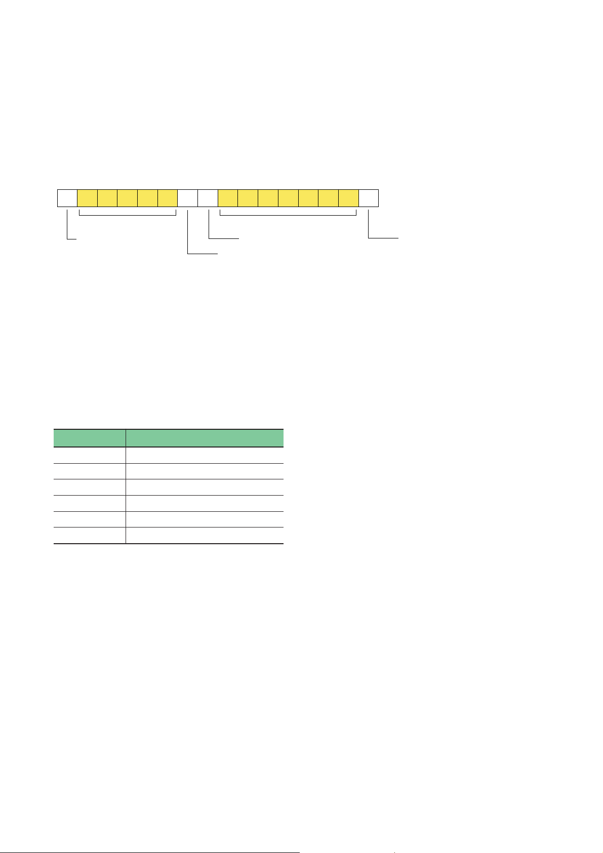
Section 4 Software Interface
4-2 Analog Output Module
3) When offset/gain adjustment mode is activated
When parameter mode is activated (when bit 15 of the module status register is set ON) and bit 6 of the parameter type setting
status register is set ON, the status of offset/gain adjustment is indicated. For this, the status of EEPROM writing completion
flag, voltage or current up/down status, and which of offset and gain values is now indicated are displayed. In this mode, offset
address +3 is unused.
* When using D300win, assign a WORD type variable to this register. If you access by the bit, assign a BOOL type variable to
each bit.
15(F) 078
+2
Unused
OFF: Offset value is
displayed
ON: Gain value is
displayed
ON: Up
Unused
ON: Down
ON: Module internal EEPROM
writing completed
(6) Mode changeover register (offset address +4)
When a value in the range from “30000” to “32767” (INT type) is input to offset address +4, parameter mode is activated. In
this mode, offset address +5 becomes the parameter type setting register, and offset addresses +6 and +7 become the
parameter setting data registers.
To change over from parameter mode to D/A conversion mode, input a digital value (smaller than “30000”) that corresponds to
the analog value to be output.
* When using D300win, assign an INT type variable to this register.
Note: When mode is changed over from “D/A conversion” to “parameter”, the value that corresponds to the digital input value of
0 (zero) is output as analog output value. The values shown in the table below may not apply when conversion
characteristic has been changed by scaling.
Output range Outputvalue in parameter mode
0to5V 0V
1to5V 1V
0to10V 0V
-10to10V 0V
4to20mA 4mA
0to20mA 0mA
4-20
Page 53
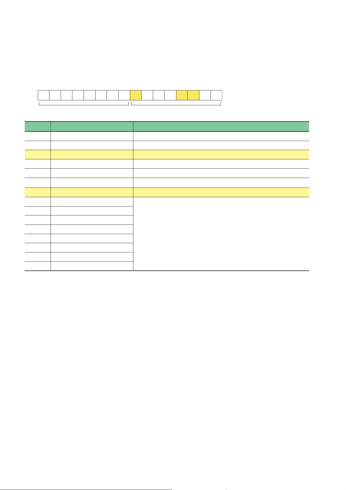
Section 4 Software Interface
4-2 Analog Output Module
(7) Parameter type setting register (offset address +5)
Parameter type and channel number for reading/writing parameters are set in this register.
* When using D300win, assign a WORD type variable to this register. If you access by the bit, assign a BOOL type variable to
each bit.
15(F) 078
+5
Channel No. Parameter type
Bit Flag name Description
0 Operation parameter read mode ON: Operation parameter read mode (allchannels in a batch)
1 Scaling parameter read mode ON: Scaling parameter read mode (individualchannel)
2, 3 Unused
4 Operation parameter write mode ON: Operation parameter write mode (all channels in a batch)
5 Scaling parameter write mode ON:Scaling parameter write mode (individual channel)
6 Offset/gain adjustment mode ON: Offset/gainadjustmentmode (indivi dual channel)
7 Unused
8 Channel 1 In "scaling parameter read mode", "scaling parameterwrite mode" or
9 Channel 2
10 Channel 3
11 Channel 4
12 Channel 5
13 Channel 6
14 Channel 7
15 Channel 8
"offset/gain adjustment mode", arbitrarychannel i s specified. In "scaling
parameter read mode", one of bits 8 to 15 is set ON to i ndicate for which
channel to set parameters. Whensame data is to be set in "scaling
parameter write mode" or "offset/gain adjustment mode", multiple arbitrary
channels may be specified.
4-21
Page 54

Section 4 Software Interface
.
4-2 Analog Output Module
(8) Parameter setting data register (offset address +6, +7)
When a value in the range from “30000” to “32767” (INT type) is input to the mode changeover register (offset address +4), bit
15 of the module status register (offset address +0) is set ON, and “parameter mode” is activated.
The set values of “operation parameter write” mode, “scaling parameter” mode or “offset/gain adjustment” mode are written in
this register.
1) When operation parameter setting mode is activated
Data is set in the locations shown below, and “operation parameter write mode flag” (bit 4 of the parameter type setting
register) is set ON.
* When using D300win, assign WORD type variables to these registers. If you access by the bit, assign a BOOL type variable
to each bit.
15(F) 0
+6
+7
Unused (fixed to 0 (zero))
Output range
Output enable/disable
OFF: Output enabled for all channels
ON: Output disabled for channels 5 to 8
<Output range>
Bit Flag name
0(L)
1(H)
2(L)
3(H)
4(L)
5(H)
6(L)
7(H)
8(L)
9(H)
10 (L)
11 (H)
12 (L)
13 (H)
14 (L)
15 (H)
Channel 1 Output range
Channel 2 Output range
Channel 3 Output range
Channel 4 Output range
Channel 5 Output range
Channel 6 Output range
Channel 7 Output range
Channel 8 Output range
Descriptio n
Output range is set bya combinationof ON/OFF status of two bits
<NP1AYH8V-MR>
H L
OFF OFF : 0 to 10 V
OFF ON : 0 to 5 V
ON OFF : 1 to 5 V
ON ON : -10 to 10 V
<NP1AYH8I-MR>
H L
OFF OFF : 4 to 20 mA
OFF ON : 0 to 20 mA
ON OFF : 4 to 20 mA
ON ON : 0 to 20 mA
2) When scaling parameter setting mode is activated
For scaling, offset and gain values are set in the locations shown below.
* When using D300win, assign INT type variables to these registers.
15(F) 0
+6
+7
<Scaling>
The analog output modules convert the digital values that are input to them by application program into analog values. The
operation to change the width (scale) of input digital values is referred to as “scaling”. The available range of scaling of these
modules is -25000 to 25000 (INT type). If a value that is out of this range is set, it will be limited to -25000 or 25000.
Offset value
Gain value
4-22
Page 55
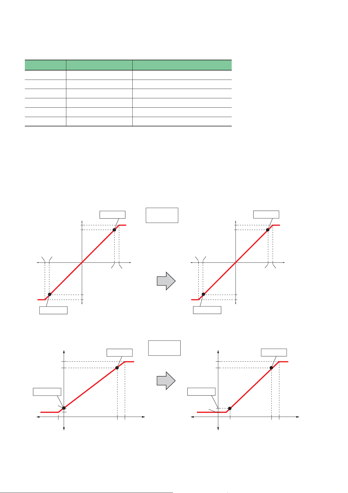
Section 4 Software Interface
4-2 Analog Output Module
<Initial value of scaling for each output range>
Output range Initial value of scaling Available range of scaling (See note.)
0 to 5 V 0 to 16000 0 to 25000
1 to 5 V 0 to 16000 0 to 25000
0 to 10 V 0 to 16000 0 to 25000
-10 to 10 V -8000 to 8000 -25000 to 25000
4 to 20 mA 0 to 16000 0 to 25000
0 to 20 mA 0 to 16000 0 to 25000
Note 1: Scaling is enabled only when the operation setting switch on the module rear panel is set to “Soft Set Range Operation
mode”. In fixed range operation mode, scaling is disabled.
Note 2: Over range is fixed to “(Gain value - Offset value) x 0.025 + Gain value”.
(“(Gain value - Offset value) x 0.0125 + Gain value” for the range of -10 to +10 V)
On the other hand, under range is fixed to “Offset value - (Gain value - Offset value) x 0.025”.
(“Offset value - (Gain value - Offset value) x 0.0125” for the range of -10 to +10 V)
Note 3: If scaling results in “resolution < maximum resolution”, digital output value does not change in steps of one.
Note 4: Once scaling values are set, they won't change even when range is changed.
<Example 1 of scaling>
Analog output voltage (V)
10.25
10
-8200 -8000
0
Offset value
<Example 2 of scaling>
Analog output current (mA)
20.4
20
-10
-10.25
Gain value
8000 8200
Gain value
Set values
Gain: 4000
Offset: -4000
Digital input
value
(INT type)
Set values
Gain: 4000
Offset: 1000
Analog output voltage (V)
10.25
10
-4200 -4000
0
Offset value
Analog output current (mA)
20.4
20
-10
-10.25
Gain value
4000 4200
Gain value
Digital input
value
(INT type)
Offset value
4
-400
0
-3.6
16000 16400
Digital input
value
(INT type)
4-23
Offset value
-3.6
4
0
1000
4000 4075
Digital input
value
(INT type)
Page 56
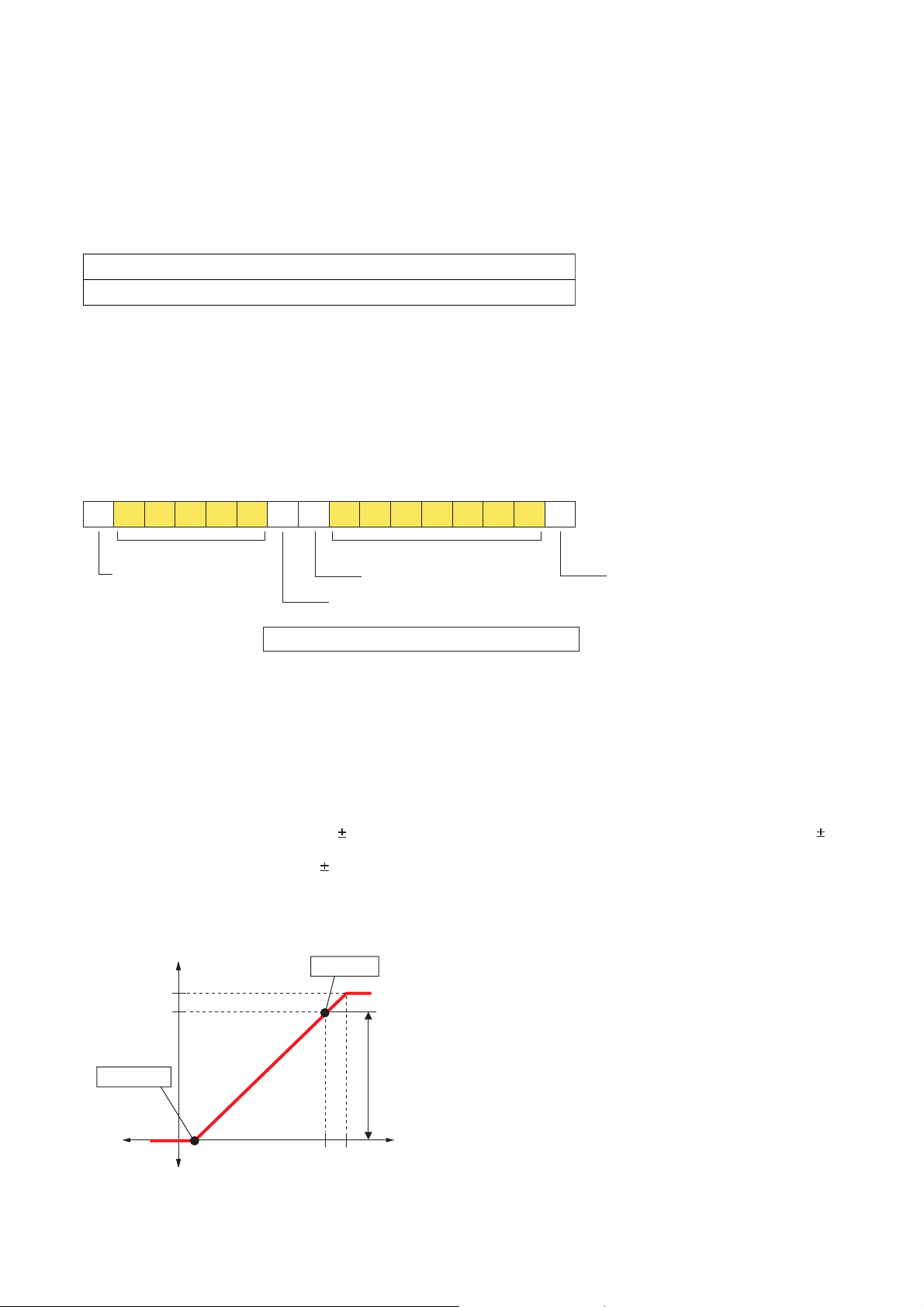
Section 4 Software Interface
4-2 Analog Output Module
<Procedure for scaling>
1) Input “30000” (INT type) to the mode changeover register (offset address +4) to activate parameter mode.
(Make sure that bit 15 of the module status register is set ON.)
2) Input gain and offset values to the parameter setting data register, and set ON bit 5 and bit 8 (in the case of channel 1) of
the parameter type setting register. (In the above example 1 of scaling, set as follows.)
15(F) 0
+6
+7
3) Make sure that bit 5 (scaling parameter write mode) and bit 8 (channel 1) of the parameter type setting register are set ON.
4) Set OFF all the bits of the parameter setting data register, and clear al the bits of the parameter setting data register to zero.
This completes the operation for scaling.
3) When offset/gain adjustment mode is activated
For offset/gain adjustment, data is set in the locations shown below:
* When using D300win, assign a WORD type variable to this register. If you access by the bit, assign a BOOL type variable to
each bit.
15(F) 078
-4000
4000
+6
Unused
OFF: Offset value is
displayed
ON: Gain value is
displayed
<Offset/gain adjustment>
In this mode, offset value and/or gain value can finely be adjusted for individual channel.
Offset value: Means the lower limit value of the range span. When this value is adjusted, the conversion characteristic curve
moves parallel in vertical direction.
Gain value: Means the upper limit value of the range span. When this value is adjusted, only gain value is changed while
offset value is kept unchanged.
When offset and gain values are changed by scaling, the values that are set by scaling take effect as offset and gain values.
When offset and/or gain values are to be adjusted after scaling, adjust by the values of scaling.
Note 1: Offset/gain adjustable range is within 1% of range span. It takes approximately 2 minutes to adjust from 0% to 1%.
If adjustment is made using an analog value that exceeds the adjustable range (if the value is input to a terminal of
the module), the value is limited to 1% of range span.
Note 2: If range is changed, offset and gain return to the default values.
Note 3: Negative current value cannot be output. If offset value is set too low, the conversion characteristic curve becomes as
follows:
Analog output current (mA)
No change when both bit 8 and bit 9 are set ON.
Gain value
ON: Down is specified
ON: Up is specified
Unused
ON: Module internal EEPROM
writing completed
20.5
20
Offset value
Practicable analog
output range
Digital input value
0
16000 16400
(INT type)
4-24
Page 57
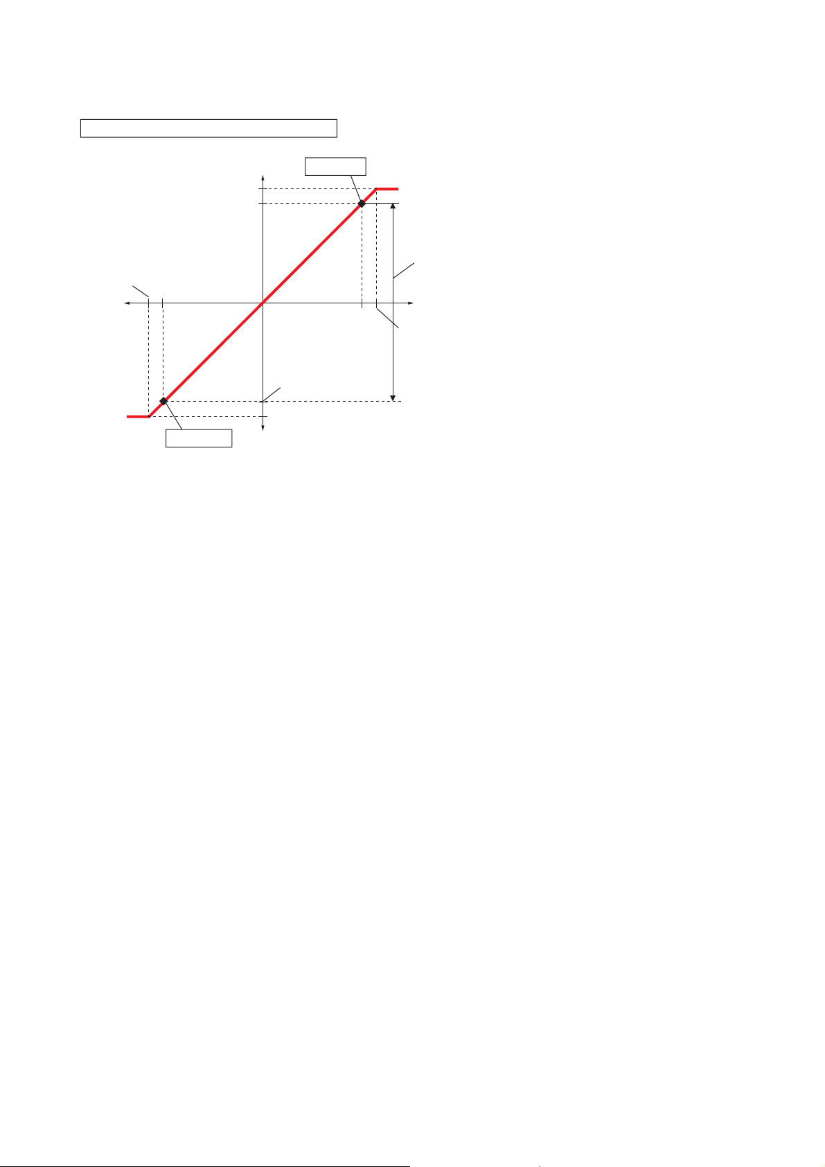
Section 4 Software Interface
4-2 Analog Output Module
Offset and gain values for the range of -10 to 10 V.
-8200
Analog output voltage (V)
10.25
10
-8000
Offset value
0
-10
-10.25
Gain value
8000
Practicable analog
output range
Digital input value
(INT type)
8200
<Offset/gain adjustment procedure>
Offset is adjusted first.
1) Input “30000” (INT type) to the mode changeover register (offset address +4) to activate parameter mode.
(Make sure that bit 15 of the module status register is set ON.)
2) Set ON bit 6 of the parameter type setting register to activate offset/gain adjustment mode. (Make sure that bit 15 of the
module status register is set ON.)
3) Set ON the bit for the channel to be adjusted (the corresponding bit of bits 8 to 15 of the parameter type setting register).
(The “SETTING” LED of the module blinks.)
4) With an external device, etc. connected to the terminal of the channel that is to be adjusted, observe the output voltage or
current value.
5) First, in the condition that bit 15 of the parameter setting data register (offset address +6) is set OFF, adjust output value by
setting ON and OFF bit 8 (output value Down) and bit 9 (output value Up).
6) After the completion of offset adjustment, set ON bit 0 (zero) of the parameter setting data register (offset address +6) to
write the offset adjustment value in the module internal EEPROM. When bit 0 (zero) of offset address +2 is set ON, the
writing of EEPROM is completed. After confirming this, set OFF bit 0 (zero) of the parameter setting data register.
7) Then set bit 15 ON of the parameter setting data register (offset address +6) and, in the same way as offset adjustment,
adjust output value by setting ON and OFF bit 8 (output value Down) and bit 9 (output value Up). (Gain adjustment)
8) After the completion of gain adjustment, set ON bit 0 (zero) of the parameter setting data register (offset address +6) to
write the gain adjustment value in the module internal EEPROM. Confirm the completion of EEPROM writing, in the same
way as explained for offset adjustment.
9) Set OFF all the bits of the parameter type setting register, and clear all the bits of the parameter setting data register to zero.
This completes the adjustment work.
[Reference]
For concrete operating method with the SX Control Utility of D300win, refer to “Appendix 1 Offset/Gain Adjustment <D300win>”.
For concrete operating method with SX-Programmer Standard, refer to “Appendix 2 Offset/Gain Adjustment <SX-Programmer
Standard>”.
4-25
Page 58

Section 4 Software Interface
4-3 Analog Input/Output Module
NP1AWH6-MR occupies 8 words of I/O area (input: 4 words, output: 4 words).
4-3-1 Memory allocation in Switch Batch Setting mode
Offset
address
15(F)
+0
Channel 1 Digital output value / Status
+1
Channel 2 Digital output value / Status
+2
Channel 3 Digital output value / Status
+3
Channel 4 Digital output value / Status
+4
Channel 5 Digital input value
+5
Channel 6 Digital input value
+6
Unused (fixed to 0 (zero))
+7
Unused (fixed to 0 (zero))
0
This module to CPU module
CPU module to this module
Status code Error Description
30002
(7532h)
30003
(7533h)
30004
(7534h)
30006
(7536h)
EEPROM calibrationdata
error (Module fatal fault)
EEPROM user setting data
error
Internal power supplydown
Conversion error
Ordinarily digital output values (INT type) are stored in the registers explained above. If the module becomes
abnormal, the following status code (INT type) is stored in these registers. When making an application program,
be sure to interlock erroneous and normal (A/D conversion) conditions.
If the calibration data ofEEPROM is destroyed or if EEPROM cannot be
writtenor read, this erroris notified. Module internalEEPROM is abnormal.
If this error occurred, it is necessary to replace the module.
If the usersetting data of EEPROM is destroyed,this erroris notified.
If this error occurred, allparameters need to be reset. If this error recurs
evenafter parameters are reset, the module seems to have failed.
If the internal power supply of the module becomes down, this error is
notified.
If conversion became abnormalbecause the module failed or was used in an
out-of-spec environment, this erroris notified.
4-26
Page 59

Section 4 Software Interface
4-3 Analog Input/Output Module
4-3-2 Memory allocation in Software Set Range Operation mode
In Software Set Range Operation mode, memory allocation differs between when operating in A/D conversion mode (during
normal operation) and when operating in parameter mode.
<When operating in conversion mode>
When operating in conversion mode, memory allocation becomes as follows:
Offset
address
15(F)
+0
Channel 1 Digital output value / Status
+1
Channel 2 Digital output value / Status
+2
Channel 3 Digital output value / Status
+3
Channel 4 Digital output value / Status
+4
Channel 5 Digital input value
+5
Channel 6 Digital input value
+6
Unused (fixed to 0 (zero))
0
This module to CPU module
CPU module to this module
+7
Unused (fixed to 0 (zero))
<When operating in parameter mode>
Parameter mode is activated when bit 7 of the parameter type setting register is set ON. In parameter mode, memory
allocation becomes as follows:
Offset
address
+0
+1
+2
+3
+4
+5
+6
+7
15(F)
Status
Parameter type setting status
Parameter read data
Parameter setting request
Parameter type setting
Parameter setting data
0
This module to CPU module
CPU module to this module
4-27
Page 60

Section 4 Software Interface
4-3 Analog Input/Output Module
(1 ) Digital output value/status register (offset address: +0 to +3)
When this module is in conversion mode, digital output values and/or statuses are stored, in the registers of offset address +0
to +3.
* When using D300win, assign INT type variables to these registers.
Offset
address
15(F)
+0
Channel 1 Digital output value / Status
+1
Channel 2 Digital output value / Status
+2
Channel 3 Digital output value / Status
+3
Channel 4 Digital output value / Status
Status code C ondition of modul Descriptio n
30002
(7532h)
30003
(7533h)
30004
(7534h)
30006
(7536h)
EEPROM calibrationdata
error
(Module fatalfault)
EEPROM user setting data
error
Internal power supplydown
Conversion error
0
If the calibration data ofEEPROM is destroyed or if EEPROMcannot be
writtenor read, this erroris notified. Module internalEEPROM is abnormal.
If this error occurred, it is necessary to replace the module.
If the usersetting data of EEPROM is destroyed,this erroris notified.
If this error occurred, allparameters need to be reset. If this error recurs
evenafter parameters are reset, the module seems to have failed.
If the internal power supply of the module becomes down, this error is
notified.
If conversion became abnormalbecause the module failed or was used in an
out-of-spec environment, this erroris notified.
Ordinarily digital output values (INT type) are stored in the registers explained above. If the module becomes
abnormal, the following status code (INT type) is stored in these registers. When making an application program,
be sure to interlock erroneous and normal (A/D conversion) conditions.
(2) Digital input values of channels 5 and 6 (offset address +4 and +5)
The digital values to undergo D/A conversion are stored in these memory areas. Just after the system is powered up, 0 V or 0
mA is output. When the initialization of the module is completed, the analog value that corresponds to the digital input value of
0 (zero) is output (for example, 1 V for the range of 1 to 5 V).
When the system is started (when the CPU module starts running), the analog value that corresponds to the digital value input
to this memory area is output. For more information of conversion characteristics, refer to “2-3 Conversion Characteristics”.
* When using D300win, assign INT type variables to these registers.
Offset
address
15(F)
+4
Channel 5 Digital input value
+5
Channel 6 Digital input value
0
(3 ) Status register (offset address +0)
When parameters are being set or read out, “30001” is output by the module.
4-28
Page 61

Section 4 Software Interface
t
4-3 Analog Input/Output Module
(4 ) Parameter type setting status register (offset address +1)
This register stores the information of what parameter is now being written or read by the module.
* When using D300win, assign a WORD type variable to this register. If you access by the bit, assign a BOOL type variable to
each bit.
15(F) 078
+1
Channel No. Parameter type
Bit Flag name Descriptio n
0 Operati on parameter read mode ON: Operationparameter read mode (allchannels in a batch)
1 Scaling parameterread mode ON: Scaling parameter read mode (indivi dual channel)
2 Operati on range parameterread mode ON: Operation range parameter read mode (all channels in a batch)
3 Unused
4 Operation parameter write mode ON: Operation parameter write mode (all channels in a batch)
5 Scaling parameter write mode ON: Scaling parameter write mode (individual channel)
6 Operati on range parameterwrite mode ON: Operation range parameter write mode (all channels in a batch)
7 Offset/gain adjustment mode ON: Offset/gain adjustment mode (individual channel)
8 Channel 1 In "scaling parameter read mode" or "scaling parameter write mode",
9 Channel 2
10 Channel 3
11 Channel 4
12 Channel 5
13 Channel 6
14 Unused
15 Unused
one of bits 8 to 15 is set ON to i ndicate whi ch channel i s nowbeing se
or read out.
(5) Parameter read data register (offset address +2 and +3)
In “operation parameter read mode”, “scaling parameter read mode”, “operation range parameter read mode”or “offset/gain
adjustment mode”, the content of the setting for the corresponding mode is stored in this register.
1) When operation parameter read mode is activated
Conversion
15(F)
Unused
+2
+3
Conversion
Moving average execution times H/L = OFF/OFF: Once, OFF/ON: Twice, ON/OFF: 4 times, ON/ON: 8 times
* When using D300win, assign WORD type variables to these registers. If you access by the bit, assign a BOOL type variable
to each bit.
13(D)
Unused
(output)
13(D)
12(C)
CH6
CH5 CH4 CH3 CH2 CH1
7 6 5 4 3 2 1 0
CH4 CH3 CH2
H L H L H L H L
enable/disable OFF:
11(B)10(A)
(output)
98
CH1
enable/disable
78
Unused
Moving average execution times
(Output)
enable, ON:
(Output)
0
disable
4-29
Page 62

Section 4 Software Interface
4-3 Analog Input/Output Module
2) When scaling parameter read mode is activated
15(F) 0
+2
+3
* When using D300win, assign INT type variables to these registers.
3) When operation range parameter read mode is activated
Offset value
Gain value
15(F) 0
+2
+3
4) When offset/gain adjustment mode is activated
* When using D300win, assign a WORD type variable to this register (offset address +2). If you access by the bit, assign a
BOOL type variable to each bit.
+2
CH4 CH3 CH2
Unused (fixed to 0 (zero))
OFF/OFF/OFF/OFF
OFF/OFF/OFF/ON
OFF/OFF/ON/OFF
OFF/OFF/ON/ON
OFF/ON/OFF/OFF
OFF/ON/OFF/ON
OFF/ON/ON/ON
Others
15(F) 0
Unused (fixed to 0 (zero))
Analog input
Offset value is displayed
OFF:
Gain valu is displayed
ON:
Analog output
Offset value is displayed
OFF:
Gain valu is displayed
ON:
Analog input operation range
CH1
CH5CH6
Analog output operation range
: 0 to 10 V
: 0 to 5 V
: 1 to 5 V
: -10 to 10 V
: 4 to 20 mA
: 0 to 20 mA
: -20 to 20 mA
: 0 to 10 V
For analog input
ON: Writing to module internal EEPROM
For analog output
ON: Writing to module internal EEPROM
ON: Down is specified.
ON: Up is specified.
+3
AD converted value (INT type)
(A converted value of a channel specified by the affset address +6 can be monitored.)
* When using D300win, assign an INT type variable to this register.
AD converted value
4-30
Page 63

Section 4 Software Interface
4-3 Analog Input/Output Module
(6) Parameter setting request (offset address +4)
When parameters are set, input a value in the range from “30000” to “32767” to this register. Make sure that the status registe r
(offset address +0) is “30001” and then set parameters.
(7) Parameter type setting register (offset address +5)
Parameter type and channel number for reading/writing parameters are set in this register.
* When using D300win, assign a WORD type variable to this register. If you access by the bit, assign a BOOL type variable to
each bit.
15(F) 078
+5
Channel No. Parameter type
Bit Flag name Descriptio n
0 Operati on parameter read mode ON: Operationparameter read mode (allchannels in a batch)
1 Scaling parameterread mode ON: Scaling parameter read mode (indivi dual channel)
2 Operati on range parameterread mode ON: Operation range parameter read mode (all channels in a batch)
3 Unused
4 Operation parameter write mode ON: Operation parameter write mode (all channels in a batch)
5 Scaling parameter write mode ON: Scaling parameter write mode (individual channel)
6 Operati on range parameterwrite mode ON: Operation range parameter write mode (all channels in a batch)
7 Offset/gain adjustment mode ON: Offset/gain adjustment mode (individual channel)
8 Channel 1 In "scaling parameter read mode", "scaling parameter write mode" or
9 Channel 2
10 Channel 3
11 Channel 4
12 Channel 5
13 Channel 6
14 Unused
15 Unused
"offset/gain adjustment mode", one of bits 8 to 15 is set ON to specify a
channel for whi ch parameters are to be set.
4-31
Page 64
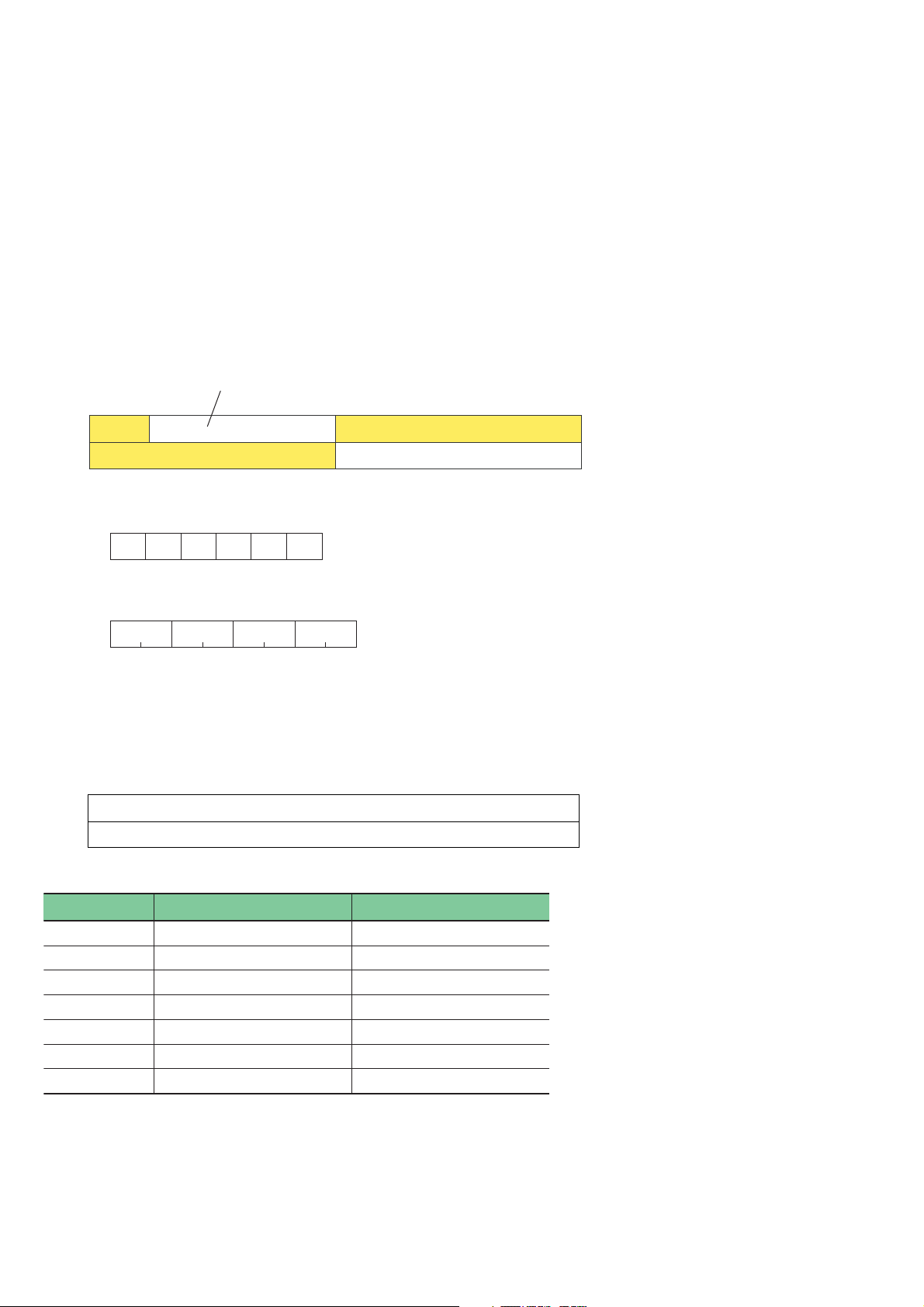
Section 4 Software Interface
4-3 Analog Input/Output Module
(8) Parameter setting data register (offset address +6 and +7)
When a value in the range from “30000” to “32767” is input to the parameter setting request register (offset address +4), the
status register (offset address +0) becomes “30001”, and “parameter” mode is activated.
The set values of “operation parameter write” mode, “scaling parameter” mode, “operation range parameter write” mode, or
“offset/gain adjustment” mode are written in this register.
If a value that is smaller than “30000” is input to this register, the mode is changed over from “parameter” mode to “conversion
mode (normal mode)”.
1) When operation parameter write mode is activated
Data is set in the locations shown below, and “operation parameter write mode flag” (bit 4 of the parameter type setting
register) is set ON.
* When using D300win, assign WORD type variables to these registers. If you access by the bit, assign a BOOL type variable
to each bit.
Conversion
15(F)
Unused
+6
+7
Conversion
Moving average execution times H/L = OFF/OFF: Once, OFF/ON: Twice, ON/OFF: 4 times, ON/ON: 8 times
2) When scaling parameter write mode is activated
For scaling, offset and gain values are set in the locations shown below, and “scaling parameter write mode flag” (bit 5 of the
parameter type setting register) is set ON.
* When using D300win, assign INT type variables to these registers.
15(F) 0
+6
+7
13(D)
Unused
(output)
13(D)
CH6
7 6 5 4 3 2 1 0
CH4 CH3 CH2
H L H L H L H L
11(B)10(A)
12(C)
CH5 CH4 CH3 CH2 CH1
(output)
enable/disable OFF:
enable/disable
98
CH1
Offset value
Gain value
78
Unused
Moving average execution times
(Output)
enable, ON:
(Output)
0
disable
<Initial value for the scaling of input range>
Input range Initial value of scaling Scaling range
0 to 5 V 0 to 16000 0 to 25000
1 to 5 V 0 to 16000 0 to 25000
0 to 10 V 0 to 16000 0 to 25000
-10 to 10 V -8000 to 8000 -25000 to 25000
4 to 20 mA 0 to 16000 0 to 25000
0 to 20 mA 0 to 16000 0 to 25000
-20 to 20 mA -8000 to 8000 -25000 to 25000
Note 1: Scaling is enabled only when the operation setting switch on the module rear panel is set to “Soft Set Range Operation
mode”. In fixed range operation mode, scaling is disabled.
Note 2: Over range is fixed to “(Gain value - Offset value) x 0.025 + Gain value”.
(“(Gain value - Offset value) x 0.0125 + Gain value” for the range of -10 to +10 V or of -20 to +20 mA)
On the other hand, under range is fixed to “Offset value - (Gain value - Offset value) x 0.025”.
(“Offset value - (Gain value - Offset value) x 0.0125” for the range of -10 to +10 V or of -20 to +20 mA)
Note 3: If scaling results in “resolution < maximum resolution”, digital output value does not change in steps of one.
Note 4: Once scaling values are set, they won't change even when range is changed in Soft Set Range Operation mode.
4-32
Page 65
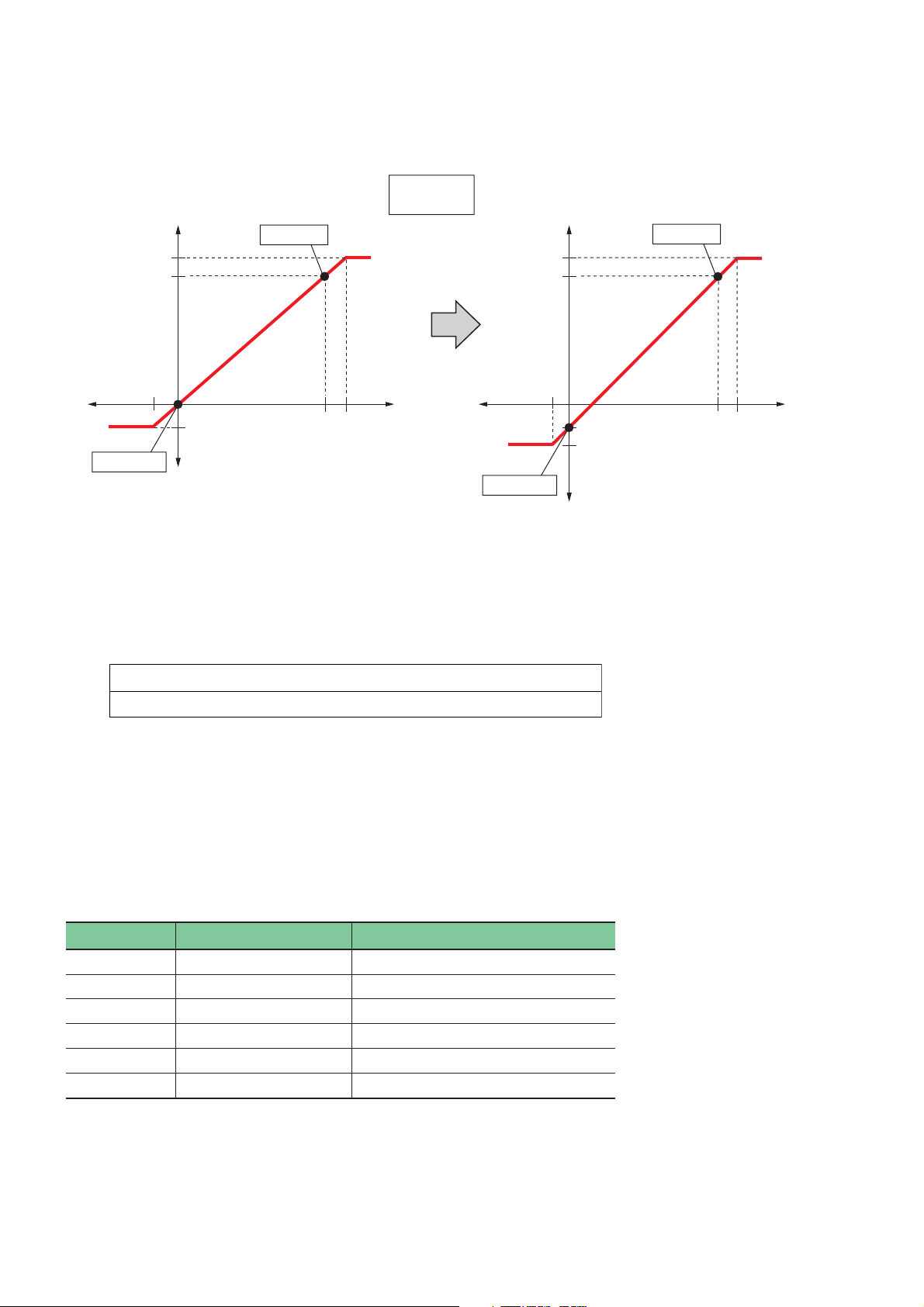
Section 4 Software Interface
4-3 Analog Input/Output Module
<Example of scaling>
Set values
Digital output value
(INT type)
Gain value
16400
16000
Gain: 4000
Offset: -1000
Digital output value
(INT type)
Gain value
4125
4000
0.5
Offset value
0
-400
20 20.4
Analog input
current (mA)
Offset value
0.5
0
-1000
-1125
Analog input
current (mA)
20 20.4
<Procedure for scaling>
1) Input “30000” to the parameter setting request register to activate parameter mode. (Make sure that the status register is
“30001”.)
2) Input gain and offset values to the parameter setting data register, and set ON bit 5 and bit 8 (in the case of channel 1) of
the parameter type setting register.
(In the above example of scaling, set as follows.)
15(F) 0
+6
+7
-1000
4000
3) Make sure that bit 5 (scaling parameter write mode) and bit 8 (channel 1) of the parameter type setting register are set ON.
4) Set OFF all the bits of the parameter type setting register, and clear all the bits of the parameter setting data register to
zero. This completes the operation for adjustment.
<Scaling for analog output>
The analog output converts the digital values that are input to them by application program into analog values. The operation to
change the width (scale) of input digital values is referred to as “scaling”. The available range of scaling of these modules is
-25000 to 25000 (INT type). If a value that is out of this range is set, it will be limited to -25000 or 25000.
<Initial value of scaling for each output range>
Output range Initial value of scaling Available range of scaling (See note.)
0 to 5 V 0 to 16000 0 to 25000
1 to 5 V 0 to 16000 0 to 25000
0 to 10 V 0 to 16000 0 to 25000
-10 to 10 V -8000 to 8000 -25000 to 25000
4 to 20 mA 0 to 16000 0 to 25000
0 to 20 mA 0 to 16000 0 to 25000
4-33
Page 66
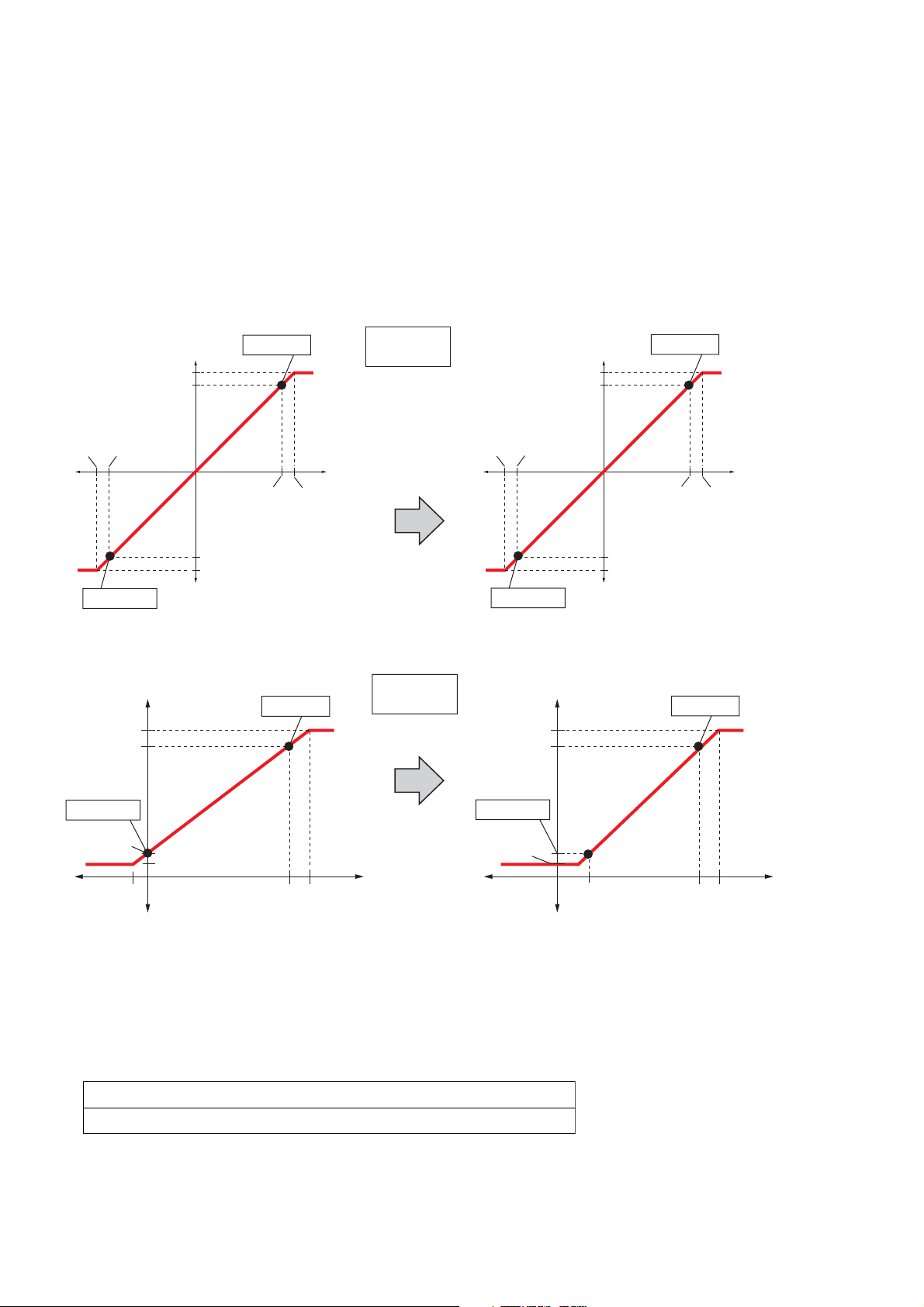
Section 4 Software Interface
4-3 Analog Input/Output Module
Note 1: Scaling is enabled only when the operation setting switch on the module rear panel is set to “Soft Set Range Operation
mode”. In fixed range operation mode, scaling is disabled.
Note 2: Over range is fixed to “(Gain value - Offset value) x 0.025 + Gain value”.
(“(Gain value - Offset value) x 0.0125 + Gain value” for the range of -10 to +10 V)
On the other hand, under range is fixed to “Offset value - (Gain value - Offset value) x 0.025”.
(“Offset value - (Gain value - Offset value) x 0.0125” for the range of -10 to +10 V)
Note 3: If scaling results in “resolution < maximum resolution”, digital output value does not change in steps of one.
Note 4: Once scaling values are set, they won't change even when range is changed.
<Example 1 of scaling>
Set values
Analog output voltage (V)
10.25
10
Gain value
Gain: 4000
Offset: -4000
Analog output voltage (V)
10.25
10
Gain value
-8200 -8000
Offset value
0
<Example 2 of scaling>
Analog output current (mA)
20.4
20
Offset value
4
-3.6
0
-400
-10
-10.25
8000 8200
Gain value
16000 16400
Digital input
value
(INT type)
Set values
Gain: 4000
Offset: 1000
Digital input
value
(INT type)
-4200 -4000
Offset value
Analog output current (mA)
20.4
20
Offset value
4
-3.6
0
0
1000
-10
-10.25
4000 4200
Gain value
4000 4075
Digital input
value
(INT type)
Digital input
value
(INT type)
<Procedure for scaling>
1) Input “30000” to the parameter setting request register (offset address +4) to activate parameter mode. (Make sure that
the status register is “30001”.)
2) Input gain and offset values to the parameter setting data register, and set ON bit 5 and bit 12 (in the case of channel 5) of
the parameter type setting register.
(In the above example 1 of scaling, set as follows.)
15(F) 0
+6
+7
-4000
4000
3) Make sure that bit 5 (scaling parameter write mode) and bit 12 (channel 5) of the parameter type setting register are set ON.
4) Set OFF all the bits of the parameter setting data register, and clear al the bits of the parameter setting data register to zero.
This completes the operation for scaling.
4-34
Page 67
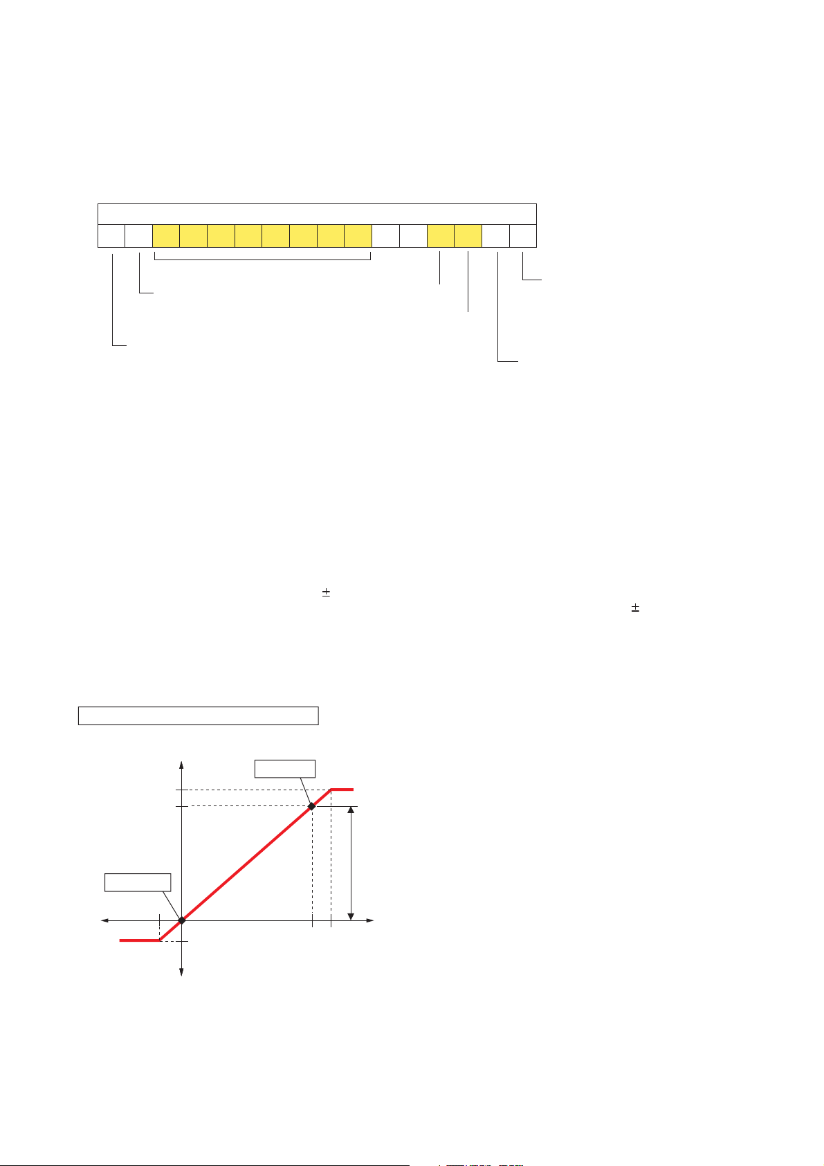
Section 4 Software Interface
4-3 Analog Input/Output Module
3) When offset/gain adjustment mode is activated
For offset/gain adjustment, data is set in the locations shown below:
* When using D300win, assign INT type variables to these registers.
15(F) 078
+6
+7
Channel No. to monitor
Free (fixed to 0 (zero))
Analog input
Offset value is displayed
OFF:
Gain value is displayed
ON:
Analog output
OFF:
Offset value is displayed
ON:
Gain value is displayed
<Analog input Offset/gain adjustment>
In this mode, offset value and/or gain value can finely be adjusted for individual channel.
Offset value: Means the lower limit value of the range span. When this value is adjusted, the conversion characteristic curve
moves parallel in vertical direction.
Gain value: Means the upper limit value of the range span. When this value is adjusted, only gain value is changed while
offset value is kept unchanged.
When offset and gain values are changed by scaling, the values that are set by scaling take effect as offset and gain values.
When offset and/or gain values are to be adjusted after scaling, adjust by the values of scaling.
Note 1: Offset/gain adjustable range is within 1% of range span. If adjustment is made using an analog value that exceeds
the adjustable range (if the value is input to a terminal of the module), the value is limited to 1% of range span.
Note 2: If range is changed, offset and gain return to the default values.
Note 3: Offset/gain adjustment is disabled when analog range is set in a batch with the switch provided on the module rear
panel.
ON: Up is specified.
ON: Down is specified.
For analog input
At the rising edge at which status
changes from OFF to ON,
adjustment values are stored in
the module internal EEPROM.
For analog output
At the rising edge at which status
changes from OFF to ON,
adjustment values are stored in
the module internal EEPROM.
<Example 1 of gain/offset adjustment>
Offset and gain values for the range of 0 to 5 V.
Digital output value
(INT type)
Gain value
16400
16000
Offset value
-0.125
0
-400
Practicable digital
output range
Analog input voltage (V)
5 5.125
4-35
Page 68
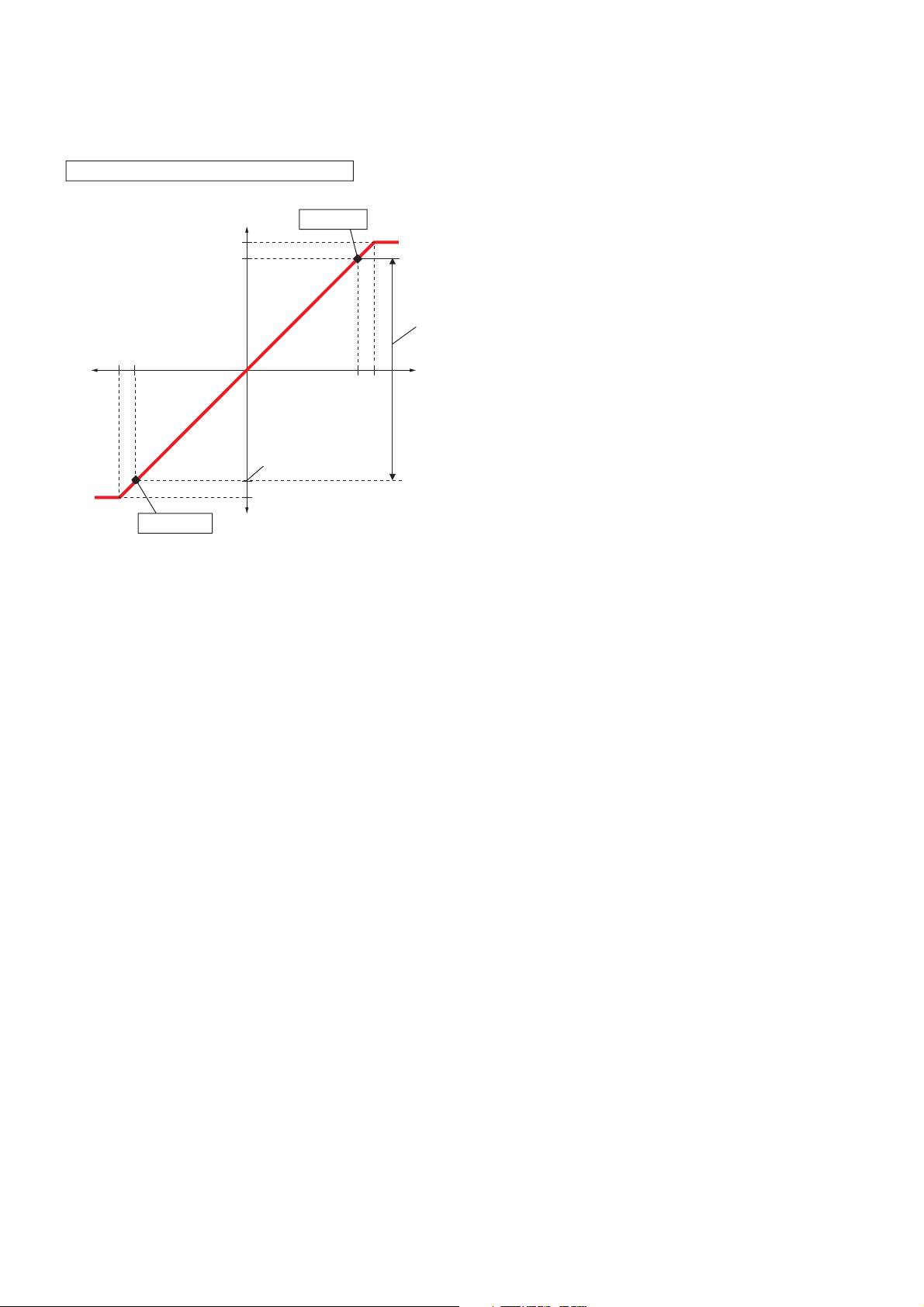
Section 4 Software Interface
4-3 Analog Input/Output Module
<Example 2 of gain/offset adjustment>
Offset and gain values for the range of -10 to 10 V.
Digital output value
-10.25 -10
(INT type)
8200
8000
0
-8200 (-125)
Offset value
Gain value
10 10.25
-8000 (0)
Practicable digital
output range
Analog input voltage (V)
<Offset/gain adjustment procedure>
Offset is adjusted first.
1) Input “30000” to the the parameter setting request register to activate parameter mode. (Make sure that the status register is
“30001”.)
2) Set ON bit 7 of the parameter type setting register to activate offset/gain adjustment mode.
3) Set ON the bit for the channel to be adjusted (the corresponding bit of bits 8 to 15 of the parameter type setting register).
(The “SETTING” LED of the module blinks.)
4) Apply a voltage (or a current) that corresponds to the offset value to the terminal of the channel that is to be adjusted.
5) Set ON bit 0 (zero) of offset address +7 of the parameter setting data register to write the offset adjustment value in the
module internal EEPROM. When bit 0 (zero) of offset address +2 is set ON, the writing of EEPROM is completed. After
confirming this, set OFF bit 0 (zero) of the parameter setting data register (offset address +7).
6) Then set bit 14 ON of offset address +7 of the parameter setting data register. (Gain adjustment of analog input)
7) Apply a voltage (or a current) that corresponds to the gain value to the terminal.
8) Set ON bit 0 (zero) of offset address +7 of the parameter type setting register to write the gain adjustment value in the
module internal EEPROM. Confirm the completion of writing in the same way as explained for offset adjustment.
9) Set OFF all the bits of the parameter type setting register, and clear all the bits of the parameter setting data register to
zero. This completes the operation for adjustment.
4-36
Page 69
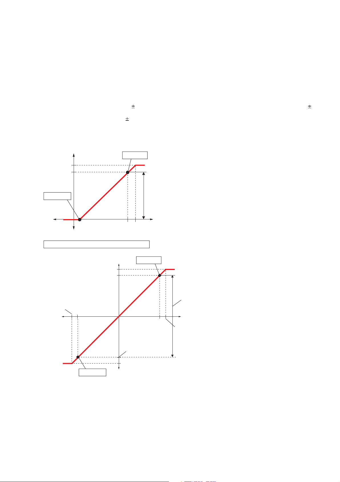
Section 4 Software Interface
4-3 Analog Input/Output Module
<Analog output Offset/gain adjustment>
In this mode, offset value and/or gain value can finely be adjusted for individual channel.
Offset value: Means the lower limit value of the range span. When this value is adjusted, the conversion characteristic curve
moves parallel in vertical direction.
Gain value: Means the upper limit value of the range span. When this value is adjusted, only gain value is changed while
offset value is kept unchanged.
When offset and gain values are changed by scaling, the values that are set by scaling take effect as offset and gain values.
When offset and/or gain values are to be adjusted after scaling, adjust by the values of scaling.
Note 1: Offset/gain adjustable range is within 1% of range span. It takes approximately 2 minutes to adjust from 0% to 1%.
If adjustment is made using an analog value that exceeds the adjustable range (if the value is input to a terminal of
the module), the value is limited to 1% of range span.
Note 2: If range is changed, offset and gain return to the default values.
Note 3: Negative current value cannot be output. If offset value is set too low, the conversion characteristic curve becomes as
follows:
Analog output current (mA)
Gain value
20.5
20
Offset value
0
Offset and gain values for the range of -10 to 10 V.
Analog output voltage (V)
-8200
-8000
16000 16400
Gain value
10.25
10
0
-10
Practicable analog
output range
Digital input value
(INT type)
8000
8200
Practicable analog
output range
Digital input value
(INT type)
Offset value
-10.25
4-37
Page 70

Section 4 Software Interface
4-3 Analog Input/Output Module
<Offset/gain adjustment procedure>
Offset is adjusted first.
1) Input “30000” to the parameter setting request register to activate the parameter mode. (Make sure that the status register
is “30001”.)
2) Set ON bit 7 of the parameter type setting register to activate offset/gain adjustment mode.
3) Set ON the bit for the channel to be adjusted (the corresponding bit of bits 12 or 13 of the parameter type setting register).
(The “SETTING” LED of the module blinks.)
4) With an external device, etc. connected to the terminal of the channel that is to be adjusted, observe the output voltage or
current value.
5) First, in the condition that bit 15 of the parameter setting data register (offset address +7) is set OFF, adjust output value by
setting ON and OFF bit 4 (output value Down) and bit 5 (output value Up).
6) After the completion of offset adjustment, set ON bit 0 (zero) of the parameter setting data register (offset address +7) to
write the offset adjustment value in the module internal EEPROM. When bit 0 (zero) of offset address +2 is set ON, the
writing of EEPROM is completed. After confirming this, set OFF bit 0 (zero) of the parameter setting data register (offset
address +7).
7) Then set bit 15 ON of the parameter setting data register (offset address +7) and, in the same way as offset adjustment,
adjust output value by setting ON and OFF bit 4 (output value Down) and bit 5 (output value Up). (Gain adjustment)
8) After the completion of gain adjustment, set ON bit 0 (zero) of the parameter setting data register (offset address +7) to
write the gain adjustment value in the module internal EEPROM. Confirm the completion of EEPROM writing, in the same
way as explained for offset adjustment.
9) Set OFF all the bits of the parameter type setting register, and clear all the bits of the parameter setting data register to zero.
This completes the adjustment work.
4-38
Page 71
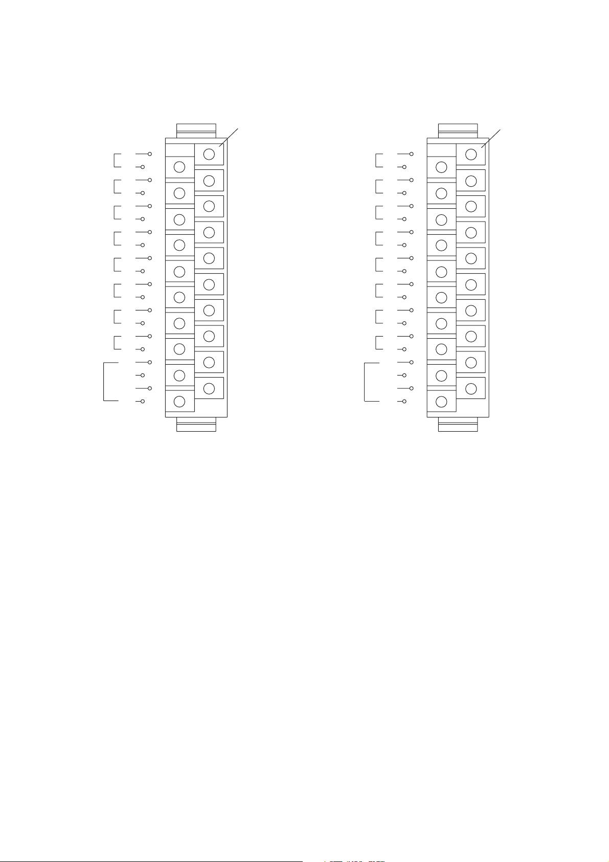
Section 5 Wiring
5-1 Wiring of Analog Input Module
5-1-1 Terminal arrangement
<NP1AXH8V-MR>
<NP1AXH8I-MR>
Channel 1
Channel 2
Channel 3
Channel 4
Channel 5
Channel 6
Channel 7
Channel 8
* Unused
terminals
CH1
CH2
CH3
CH4
CH5
CH6
CH7
CH8
V+
V-
V+
V-
V+
V-
V+
V-
V+
V-
V+
V-
V+
V-
V+
V-
N.C.
N.C.
N.C.
N.C.
10
12
16
18
14
20
Terminal No.
CH1
CH2
CH3
CH4
CH5
CH6
CH7
CH8
I+
I-
I+
I-
I+
I-
I+
I-
I+
I-
I+
I-
I+
I-
I+
I-
N.C.
N.C.
N.C.
N.C.
1
2
3
4
5
6
7
8
9
10
11
12
13
14
15
16
17
18
19
20
1
2
3
4
5
6
7
8
9
11
13
15
Channel 1
Channel 2
Channel 3
Channel 4
Channel 5
Channel 6
Channel 7
Channel 8
17
* Unused
19
terminals
Terminal No.
* Unused terminals can be used as dummy termination for shielding wires or analog signal cables.
5-1
Page 72
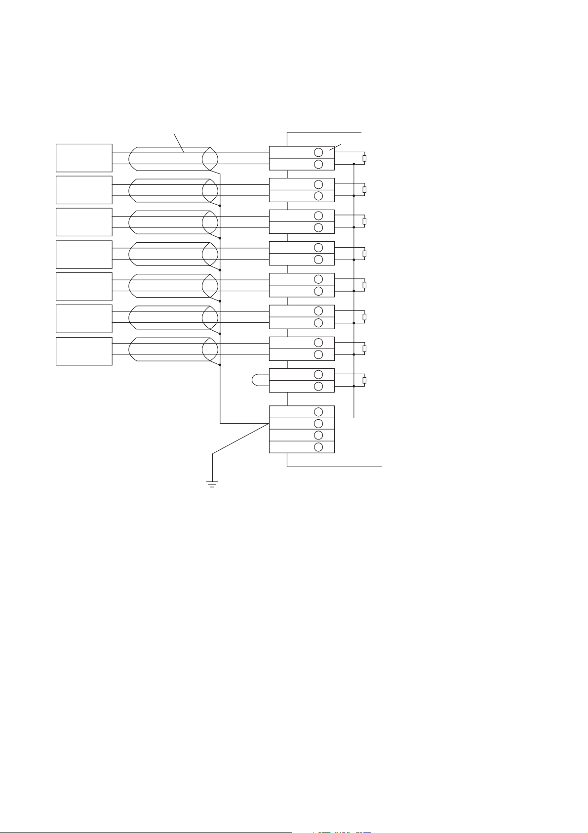
Section 5 Wiring
5-1 Wiring of Analog Input Module
5-1-2 Wiring example
The analog input modules shall be wired according to the figure below, using shielded twisted pair cables.
Analog
output device
Analog
output device
Analog
output device
Analog
output device
Analog
output device
Analog
output device
Analog
output device
Shielded twisted pair cable
(Note 1)
Analog input module
V+/I+
V-/I-
V+/I+
V-/I-
V+/I+
V-/I-
V+/I+
V-/I-
V+/I+
V-/I-
V+/I+
V-/I-
V+/I+
V-/I-
V+/I+
V-/I-
NC
NC
NC
NC
1
2
3
4
5
6
7
8
9
10
11
12
13
14
15
16
17
18
19
20
Terminal No.
(Note 2)
Note 1: Unused channels shall basically be short-circuited.
Note 2: Ground shielding wires at one point on the PC side (class D grounding). However, when shielding wires had better
be grounded on the external device side due to the condition of external noise, their ends on the module side must be
open. For grounding, NC terminals can be used as dummy termination for shielding wires. However, they must not
be used as dummy termination for other control signal cables or power cables.
Note 3: Keep signal wires that go out of this module sufficiently away from high-voltage or power cables, and avoid parallel
wiring.
Note 4: Avoid wiring the signal cables in the vicinity of load cables coming from devices other than PLC or bundling them with
such cables.
Note 5: Keep the signal cables sufficiently away from circuits where high frequencies occur, such as inverter main load circuit.
5-2
Page 73
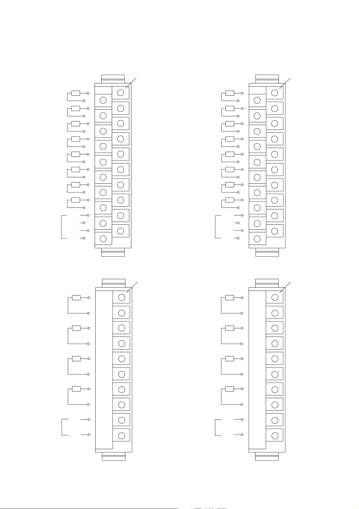
Section 5 Wiring
5-2 Wiring of Analog Output Module
5-2-1 Terminal arrangement
<NP1A YH8V-MR>
<NP1AYH8I-MR>
Channel 1
Channel 2
Channel 3
Channel 4
Channel 5
Channel 6
Channel 7
Channel 8
* Unused
terminals
CH1
CH2
CH3
CH4
CH5
CH6
CH7
CH8
N.C.
N.C.
N.C.
N.C.
Terminal No.
V+
V-
V+
V-
V+
V-
V+
V-
V+
V-
10
V+
V-
12
V+
V-
V+
V-
16
14
1
2
3
4
Channel 1
Channel 2
5
6
7
8
Channel 3
Channel 4
9
Channel 5
11
13
15
Channel 6
Channel 7
Channel 8
CH1
CH2
CH3
CH4
CH5
CH6
CH7
CH8
17
18
19
* Unused
terminals
20
N.C.
N.C.
N.C.
N.C.
I+
I-
I-
I-
I-
I-
I-
I-
I-
2
I+
4
I+
6
I+
8
I+
10
I+
I+
I+
11
12
13
14
15
16
17
18
19
20
Terminal No.
1
3
5
7
9
<NP1A YH4V-MR> <NP1AYH4I-MR>
Terminal No.
Channel 1
Channel 2
Channel 3
Channel 4
* Unused
terminals
CH1
CH2
CH3
CH4
N.C.
N.C.
V+
V-
V+
V-
V+
V-
V+
V-
10
1
Channel 1
2
3
Channel 2
4
5
Channel 3
6
7
Channel 4
8
9
* Unused
terminals
CH1
CH2
CH3
CH4
N.C.
N.C.
Terminal No.
I+
I-
I+
I-
I+
I-
I+
I-
1
2
3
4
5
6
7
8
9
10
* Unused terminals can be used as dummy termination for shielding wires or analog signal cables.
5-3
Page 74

Section 5 Wiring
5-2 Wiring of Analog Output Module
5-2-2 Wiring example
The analog output modules shall be wired according to the figure below, using shielded twisted pair cables.
Analog input module
Terminal No.
Shielded twisted pair cable
1
V+/I+
2
V-/I-
3
V+/I+
4
V-/I-
5
V+/I+
6
V-/I-
7
V+/I+
8
V-/I-
9
V+/I+
10
V-/I-
11
V+/I+
12
V-/I-
13
V+/I+
14
V-/I-
15
V+/I+
16
V-/I-
CH1
Analog Device
CH2
Analog Device
CH3
Analog Device
CH4
Analog Device
CH5
Analog Device
CH6
Analog Device
CH7
Analog Device
CH8
(Note 1)
17
NC
18
NC
19
NC
20
NC
(Note 2)
Note 1: Unused channels shall basically be opened when the voltage output module is used or short-circuited when the
current output module is used.
Note 2: Shielding wires shall be grounded basically on the external device side (class D grounding). When shielding wires
are grounded on the analog output module side (class D grounding) due to the condition of external noise, NC
terminals can be used as dummy termination for shielding wires. However, they must not be used as dummy
termination for other control signal cables or power cables.
Note 3: Keep signal wires that go out of this module sufficiently away from high-voltage or power cables, and avoid parallel
wiring.
Note 4: Avoid wiring the signal cables in the vicinity of load cables coming from devices other than PLC or bundling them with
such cables.
Note 5: Keep the signal cables sufficiently away from circuits where high frequencies occur, such as inverter main load circuit.
5-4
Page 75

Section 5 Wiring
5-3 Wiring of Analog Input/Output Module
5-3-1 Terminal arrangement
Terminal No.
Channel 1
Channel 2
Channel 3
Channel 4
Channel 5
Channel 6
V1
COM1
I1
V2
COM2
I2
V3
COM3
I3
V4
COM4
I4
V5
COM5
I5
V6
COM6
I6
SLD
SLD
1
2
3
4
5
6
7
8
9
10
11
12
13
14
15
16
17
18
19
20
5-5
Page 76

Section 5 Wiring
5-3 Wiring of Analog Input/Output Module
5-3-2 Wiring example
The analog input/output module shall be wired according to the figure below, using shielded twisted pair cables.
Analog
output device
Analog
output device
Analog
output device
Analog
output device
Analog
input device
Analog
input device
Current input
Shielded twisted pair cable
* 1
* 2
Analog input/output module
V1
COM1
I1
V2
COM2
I2
V3
COM3
I3
V4
COM4
I4
V5
COM5
I5
V6
COM6
I6
SLDޓ
SLDޓ
1
2
3
4
5
6
7
8
9
10
11
12
13
14
15
16
17
18
19
20
Terminal No.
When current is input,
short-circuit between “V” and “I”.
* 1 When voltage is output, connect
between “V” and “COM” terminals.
* 2 When current is output, connect
between “I” and “COM” terminals.
Connected internally
(Note 2)
Note 1: Unused channels shall basically be short-circuited and output terminals shall be open.
Note 2: Ground shielding wires at one point on the PC side (class D grounding). However, when shielding wires had better
be grounded on the external device side due to the condition of external noise, their ends on the module side must be
open. If an external input device has the same FG, it may be better to ground both sides.
Note 3: Keep signal wires that go out of this module sufficiently away from high-voltage or power cables, and avoid parallel
wiring.
Note 4: Avoid wiring the signal cables in the vicinity of load cables coming from devices other than PLC or bundling them with
such cables.
Note 5: Keep the signal cables sufficiently away from circuits where high frequencies occur, such as inverter main load circuit.
5-6
Page 77

Appendix 1 Offset/Gain Adjustment <D300win>
Appendix 1-1 Offset/Gain Adjustment of Analog Input Module
<Offset/gain adjustment>
In this mode, offset value and/or gain value can finely be adjusted for individual channel.
Offset value: Means the lower limit value of the range span. When this value is adjusted, the conversion characteristic curve
moves parallel in vertical direction.
Gain value: Means the upper limit value of the range span. When this value is adjusted, only gain value is changed while
offset value is kept unchanged.
When offset and gain values are changed by scaling, the values that are set by scaling take effect as offset and gain values.
When offset and/or gain values are to be adjusted after scaling, adjust by the values of scaling.
Note 1: Offset/gain adjustable range is within 1% of range span. If adjustment is made using an analog value that exceeds
the adjustable range (if the value is input to a terminal of the module), the value is limited to 1% of range span.
Note 2: If range is changed, offset and gain return to the default values.
Note 3: Offset/gain adjustment is disabled when analog range is set in a batch with the switch provided on the module rear
panel.
Offset and gain values for the range of 0 to 5 V.
Digital output value
(INT type)
Gain value
16400
16000
Practicable digital
output range
Offset value
-0.125
0
-400
5 5.125
Analog input voltage (V)
<Offset/gain adjustment with SX Control Utility of D300win>
1) Start SX Control Utility to monitor the input/output areas of the analog input module that is to be adjusted.
Input/output status of
analog input module
App.1-1
Page 78

Appendix 1 Offset/Gain Adjustment <D300win>
Appendix 1-1 Offset/Gain Adjustment of Analog Input Module
2) Offset is adjusted first.
Set ON bit 7 and bit 6 of the parameter type setting register (offset address +8) to activate offset/gain adjustment mode.
Bit 6 of the parameter type setting status register (offset address +1)
is set ON, indicating that offset/gain adjustment mode is activated.
Make sure that module
status is "30001".
3) Set ON the bit for the channel that is to be adjusted (the corresponding one of bits 8 to 15 of the parameter type setting
register). (The "SETTING" LED of the module starts blinking.)
The bit of the parameter type
setting status register that
corresponds to the channel to
be adjusted is set ON. In this
example, bit 8 (channel 1) is
set ON.
Channel 8 Channel 7 Channel 6 Channel 5 Channel 4 Channel 3 Channel 2 Channel 1
App.1-2
Page 79

Appendix 1 Offset/Gain Adjustment <D300win>
Appendix 1-1 Offset/Gain Adjustment of Analog Input Module
4) Apply a voltage (or a current) that corresponds to the offset value to the terminal of the channel that is to be adjusted.
Set ON bit 0 (zero) of the parameter setting data register (offset address +0) to write the offset adjustment value in the
module internal EEPROM. The completion of EEPROM writing can be confirmed by that bit 0 (zero) of offset address +2 is
set ON.
Completion of EEPROM writing
EEPROM write command
5) After confirming that the data is written in the EEPROM, set OFF bit 0 (zero) of offset address +10 of the parameter type
setting register.
App.1-3
Page 80
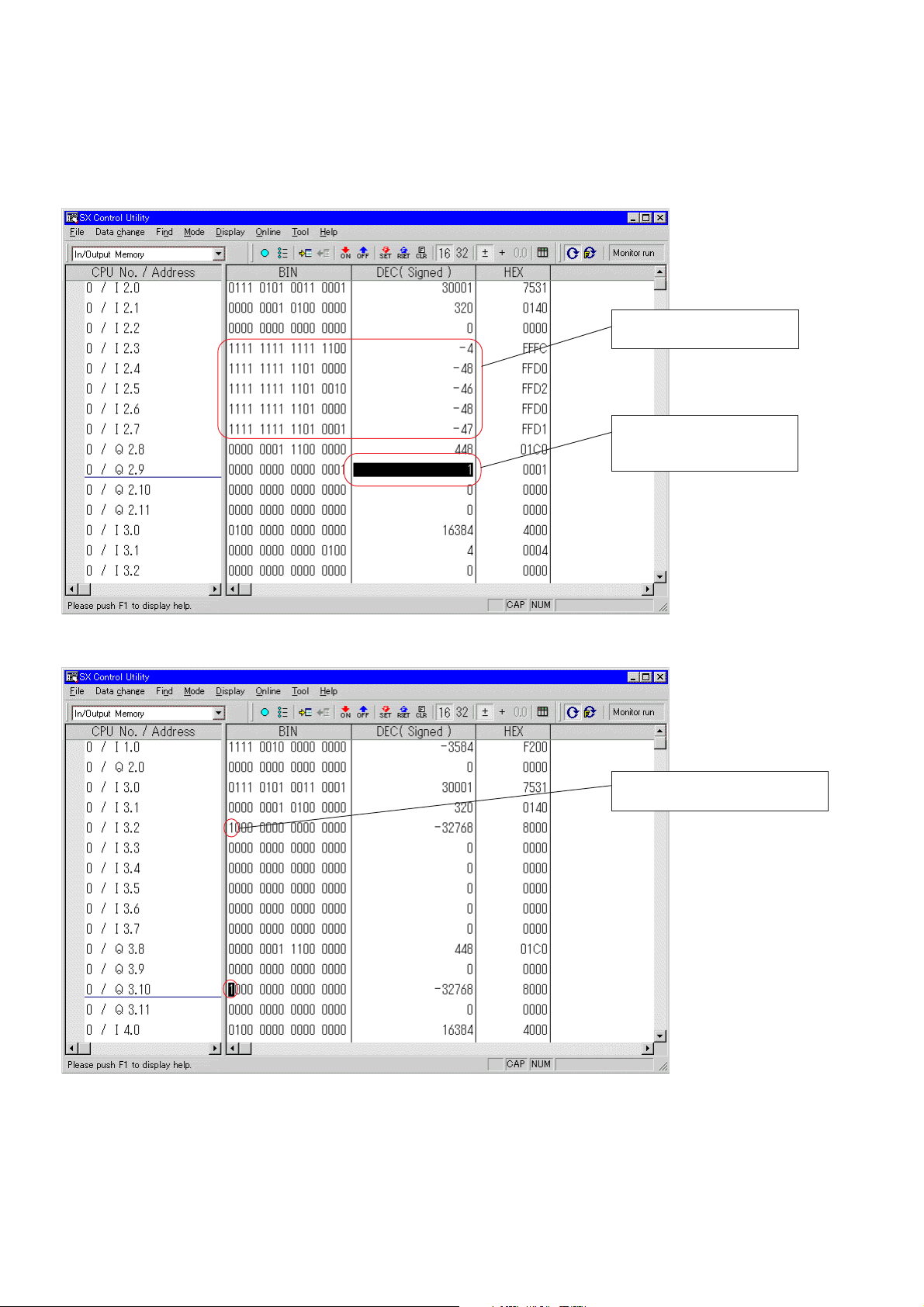
Appendix 1 Offset/Gain Adjustment <D300win>
Appendix 1-1 Offset/Gain Adjustment of Analog Input Module
6) When offset/gain adjustment mode is activated, offset adjustment value can be monitored.
Input the first channel number of the channels that are to be monitored to the parameter setting data register (offset
address +9), and the statuses of offset values for 5 channels will be displayed in the fields for offset addresses +3 to +7 of
the parameter read data register. (Gain adjustment values can be monitored in the same way.)
The statuses of offset values
can be monitored.
Set “1” (one) when you want
to monitor channel 1 (one)
and following channels.
7) Set ON bit 15 of the parameter type setting register and adjust gain.
Bit 15 of the parameter type setting
status register is set ON.
App.1-4
Page 81
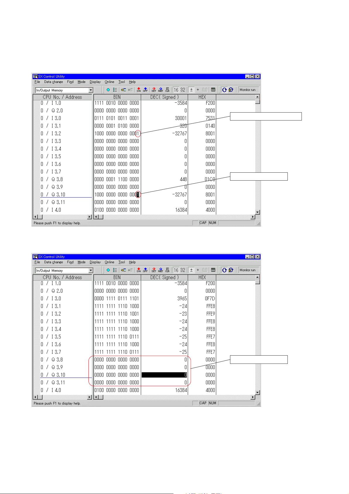
Appendix 1 Offset/Gain Adjustment <D300win>
Appendix 1-1 Offset/Gain Adjustment of Analog Input Module
8) Apply a voltage (or a current) that corresponds to the gain adjustment value to the terminal.
Set ON bit 0 (zero) of offset address +10 of the parameter type setting register to write gain adjustment value in the module
internal EEPROM. Confirm the completion of EEPROM writing in the same way as offset adjustment.
Completion of EEPROM writing
EEPROM write command
9) Set OFF all the bits of the parameter type setting register and clear all the bits of the parameter setting data register to zero.
This completes the adjustment work.
Clear all these to zero.
App.1-5
Page 82
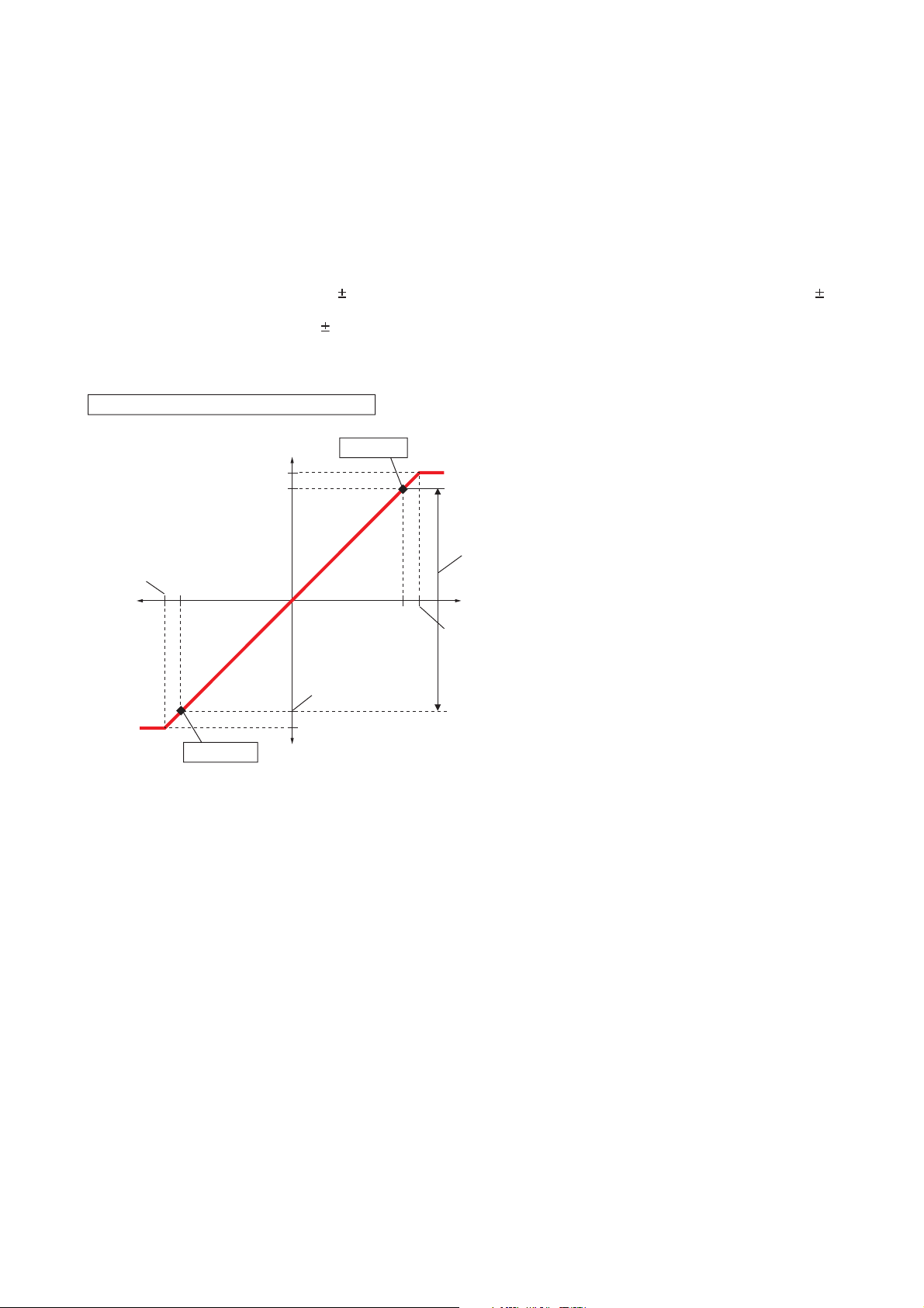
Appendix 1 Offset/Gain Adjustment <D300win>
Appendix 1-2 Offset/Gain Adjustment of Analog Output Module
<Offset/gain adjustment>
In this mode, offset value and/or gain value can finely be adjusted for individual channel.
Offset value: Means the lower limit value of the range span. When this value is adjusted, the conversion characteristic
curve moves parallel in vertical direction.
Gain value: Means the upper limit value of the range span. When this value is adjusted, only gain value is changed while
offset value is kept unchanged.
When offset and gain values are changed by scaling, the values that are set by scaling take effect as offset and gain values.
When offset and/or gain values are to be adjusted after scaling, adjust by the values of scaling.
Note 1: Offset/gain adjustable range is within 1% of range span. It takes approximately 2 minutes to adjust from 0% to 1%.
If adjustment is made using an analog value that exceeds the adjustable range (if the value is input to a terminal of
the module), the value is limited to 1% of range span.
Note 2: If range is changed, offset and gain return to the default values.
Note 3: The current output modules cannot output negative current value.
Offset and gain values for the range of -10 to 10 V.
8200
Analog output voltage (V)
10.25
10
-8000
Offset value
0
-10
-10.25
Gain value
8000
Practicable analog
output range
Digital input value
(INT type)
8200
App.1-6
Page 83
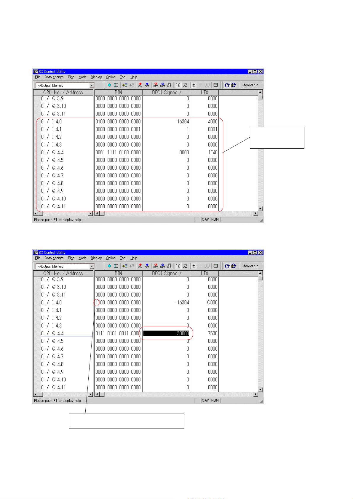
Appendix 1 Offset/Gain Adjustment <D300win>
Appendix 1-2 Offset/Gain Adjustment of Analog Output Module
<Offset/gain adjustment with SX Control Utility of D300win>
1) Start SX Control Utility to monitor the input/output areas of the analog output module that is to be adjusted.
Input/output status of
analog output module
(of 8ch specification)
2) Offset is adjusted first.
Input a value in the range from "30000" to "32767" to offset address +4 to change mode.
Make sure that bit 15 of the module status register
(offset address +0) is set ON (parameter mode).
App.1-7
Page 84
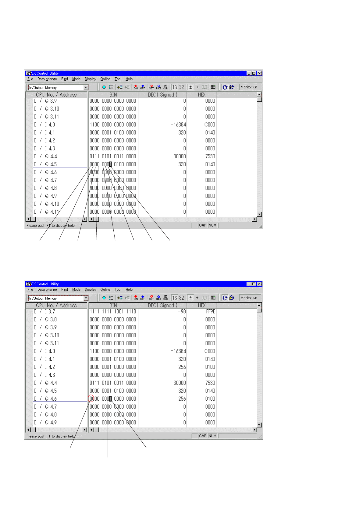
Appendix 1 Offset/Gain Adjustment <D300win>
Appendix 1-2 Offset/Gain Adjustment of Analog Output Module
3) Set ON bit 6 of the parameter type setting register (offset address +5) to activate offset/gain adjustment mode, and set ON
the bit for the channel that is to be adjusted (the corresponding one of bits 8 to 15 of the parameter type setting register).
Channel 8 Channel 7 Channel 6 Channel 5 Channel 4 Channel 3 Channel 2 Channel 1
4) With an external device, etc. connected to the terminal of the channel to be adjusted, observe output voltage or current value.
First, in the condition that bit 15 of the parameter setting data register (offset address +6) is set OFF, adjust output value by
setting ON and OFF bit 8 (output value Down) and bit 9 (output value Up).
0: Offset value adjustment
Output value Up
* While the output value up bit and down bit are on, the values change. (1% per 2minutes)
Output value Down
App.1-8
Page 85
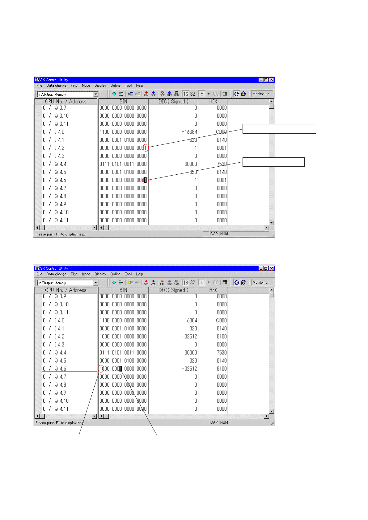
Appendix 1 Offset/Gain Adjustment <D300win>
Appendix 1-2 Offset/Gain Adjustment of Analog Output Module
5) After the completion of offset adjustment, set ON bit 0 (zero) of the parameter setting data register (offset address +6) to
write the offset adjustment value in the module internal EEPROM. When bit 0 (zero) of offset address +2 is set ON, the
writing of EEPROM is completed. After confirming this, set OFF bit 0 (zero) of the parameter setting data register.
Completion of EEPROM writing
EEPROM write command
6) Then set bit 15 ON of the parameter setting data register (offset address +6) and, in the same way as offset adjustment,
adjust output value by setting ON and OFF bit 8 (output value Down) and bit 9 (output value Up). (Gain adjustment)
0: Offset value adjustment
Output value Up
* While the output value up bit and down bit are on, the values change. (1% per 2minutes)
Output value Down
App.1-9
Page 86
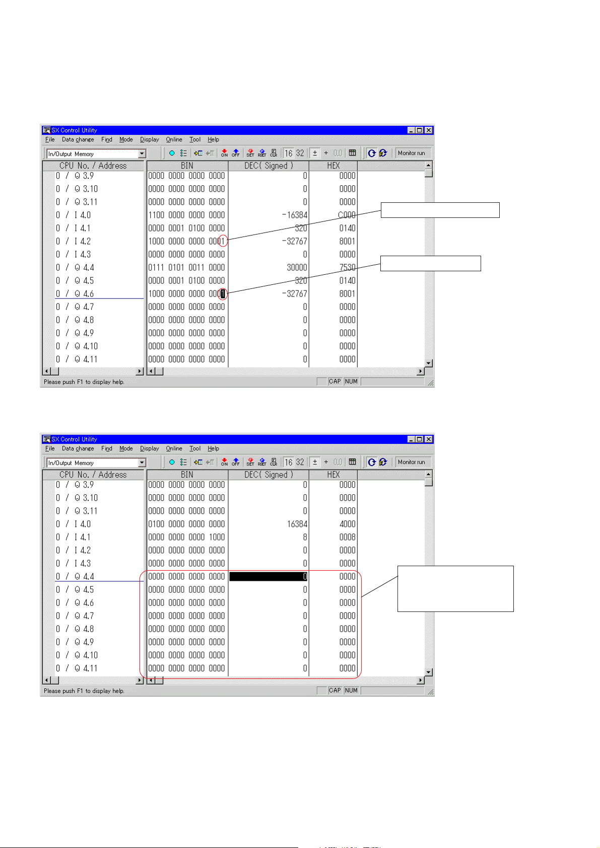
Appendix 1 Offset/Gain Adjustment <D300win>
Appendix 1-2 Offset/Gain Adjustment of Analog Output Module
7) After the completion of gain adjustment, set ON bit 0 (zero) of the parameter setting data register (offset address +6) to write
the gain adjustment value in the module internal EEPROM. Confirm the completion of EEPROM writing, in the same way as
explained for offset adjustment.
Completion of EEPROM writing
EEPROM write command
8) Set OFF all the bits of the parameter type setting register, and clear all the bits of the parameter setting data register to zero.
This completes the adjustment work.
Clear all these to zero.
Finally clear the mode
changeover register
(offset address +4) to zero.
App.1-10
Page 87
Appendix 2 Offset/Gain Adjustment <SX-Programmer S t andard>
Appendix 2-1 Offset/Gain Adjustment of Analog Input Module
<Offset/gain adjustment>
In this mode, offset value and/or gain value can finely be adjusted for individual channel.
Offset value: Means the lower limit value of the range span. When this value is adjusted, the conversion characteristic
curve moves parallel in vertical direction.
Gain value: Means the upper limit value of the range span. When this value is adjusted, only gain value is changed while
offset value is kept unchanged.
When offset and gain values are changed by scaling, the values that are set by scaling take effect as offset and gain values.
When offset and/or gain values are to be adjusted after scaling, adjust by the values of scaling.
Note 1: Offset/gain adjustable range is within 1% of range span. If adjustment is made using an analog value that exceeds
the adjustable range (if the value is input to a terminal of the module), the value is limited to 1% of range span.
Note 2: If range is changed, offset and gain return to the default values.
Note 3: Offset/gain adjustment is disabled when analog range is set in a batch with the switch provided on the module rear
panel.
Offset and gain values for the range of 0 to 5 V.
Digital output value
(INT type)
Gain value
16400
16000
Practicable digital
output range
Offset value
-0.125
0
-400
5 5.125
Analog input voltage (V)
<Offset/gain adjustment with the data monitor and the setting function of SX-Programmer Standard>
1) Connect the loader to the PLC online to monitor the input/output areas of the analog input module that is to be adjusted.
App.2-1
Input/output status of
analog input module
Page 88
Appendix 2 Offset/Gain Adjustment <SX-Programmer S t andard>
Appendix 2-1 Offset/Gain Adjustment of Analog Input Module
2) Offset is adjusted first.
Set ON bit 7 and bit 6 of the parameter type setting register (offset address +8) to activate offset/gain adjustment mode.
Bit 6 of the parameter type setting status register (offset address +1)
is set ON, indicating that offset/gain adjustment mode is activated.
3) Set ON the bit for the channel that is to be adjusted (the corresponding one of bits 8 to 15 of the parameter type setting
register). (The "SETTING" LED of the module starts blinking.)
The bit of the parameter type setting status register
that corresponds to the channel to be adjusted is set
ON. In this example, bit 8 (channel 1) is set ON.
Make sure that module
status is “30001”.
Channel 8 Channel 7 Channel 6 Channel 5 Channel 4 Channel 3 Channel 2 Channel 1
App.2-2
Page 89
Appendix 2 Offset/Gain Adjustment <SX-Programmer S t andard>
Appendix 2-1 Offset/Gain Adjustment of Analog Input Module
4) Apply a voltage (or a current) that corresponds to the offset value to the terminal of the channel that is to be adjusted.
Set ON bit 0 (zero) of the parameter setting data register (offset address +0) to write the offset adjustment value in the
module internal EEPROM. The completion of EEPROM writing can be confirmed by that bit 0 (zero) of offset address +2 is
set ON.
Completion of EEPROM writing
EEPROM write command
5) After confirming that the data is written in the EEPROM, set OFF bit 0 (zero) of offset address +10 of the parameter type
setting register.
App.2-3
Page 90

Appendix 2 Offset/Gain Adjustment <SX-Programmer S t andard>
Appendix 2-1 Offset/Gain Adjustment of Analog Input Module
6) When offset/gain adjustment mode is activated, offset adjustment value can be monitored.
Input the first channel number of the channels that are to be monitored to the parameter setting data register (offset
address +9), and the statuses of offset values for 5 channels will be displayed in the fields for offset addresses +3 to +7 of
the parameter read data register. (Gain adjustment values can be monitored in the same way.)
The statuses of offset
values can be monitored.
7) Set ON bit 15 of the parameter type setting register and adjust gain.
Bit 15 of the parameter type
setting status register is set ON.
Set “1” (one) when you want to monitor
channel 1 (one) and following channels.
App.2-4
Page 91
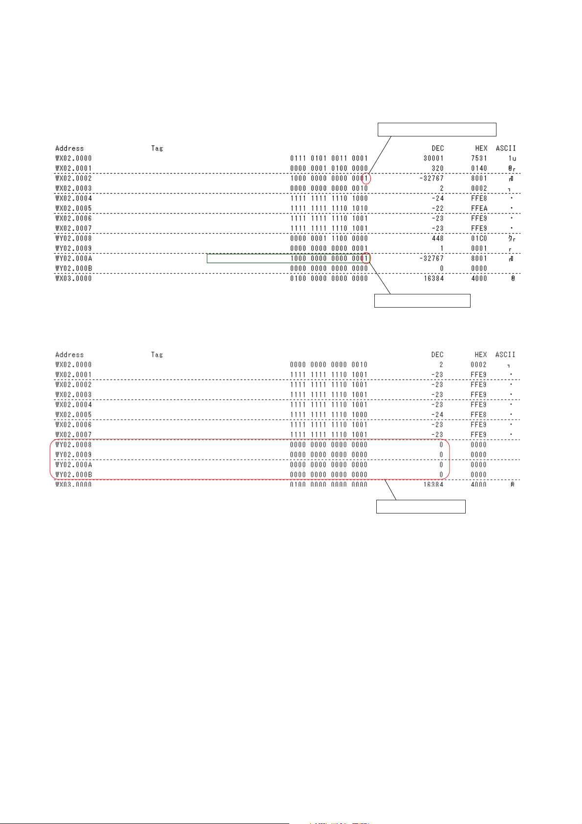
Appendix 2 Offset/Gain Adjustment <SX-Programmer S t andard>
Appendix 2-1 Offset/Gain Adjustment of Analog Input Module
8) Apply a voltage (or a current) that corresponds to the gain adjustment value to the terminal.
Set ON bit 0 (zero) of offset address +10 of the parameter type setting register to write gain adjustment value in the module
internal EEPROM. Confirm the completion of EEPROM writing in the same way as offset adjustment.
Completion of EEPROM writing
EEPROM write command
9) Set OFF all the bits of the parameter type setting register and clear all the bits of the parameter setting data register to zero.
This completes the adjustment work.
Clear all these to zero.
App.2-5
Page 92

Appendix 2 Offset/Gain Adjustment <SX-Programmer S t andard>
Appendix 2-2 Offset/Gain Adjustment of Analog Output Module
<Offset/gain adjustment>
In this mode, offset value and/or gain value can finely be adjusted for individual channel.
Offset value: Means the lower limit value of the range span. When this value is adjusted, the conversion characteristic
curve moves parallel in vertical direction.
Gain value: Means the upper limit value of the range span. When this value is adjusted, only gain value is changed while
offset value is kept unchanged.
When offset and gain values are changed by scaling, the values that are set by scaling take effect as offset and gain values.
When offset and/or gain values are to be adjusted after scaling, adjust by the values of scaling.
Note 1: Offset/gain adjustable range is within 1% of range span. It takes approximately 2 minutes to adjust from 0% to 1%.
If adjustment is made using an analog value that exceeds the adjustable range (if the value is input to a terminal of
the module), the value is limited to 1% of range span.
Note 2: If range is changed, offset and gain return to the default values.
Note 3: The current output modules cannot output negative current value.
Offset and gain values for the range of -10 to 10 V.
8200
Analog output voltage (V)
10.25
10
-8000
Offset value
0
-10
-10.25
Gain value
8000
Practicable analog
output range
Digital input value
(INT type)
8200
App.2-6
Page 93

Appendix 2 Offset/Gain Adjustment <SX-Programmer S t andard>
Appendix 2-2 Offset/Gain Adjustment of Analog Output Module
<Offset/gain adjustment with SX Control Utility of D300win>
1) Connect a loader to a PLC online to monitor the input/output areas of the analog input module that is to be adjusted.
Input/output status of analog output
module (of 8ch specification)
2) Offset is adjusted first.
Input a value in the range from "30000" to "32767" to offset address +4 to change mode.
Make sure that bit 15 of the module status register
(offset address +0) is set ON (parameter mode).
3) Set ON bit 6 of the parameter type setting register (offset address +5) to activate offset/gain adjustment mode, and set ON
the bit for the channel that is to be adjusted (the corresponding one of bits 8 to 15 of the parameter type setting register).
Channel 8 Channel 7 Channel 6 Channel 5 Channel 4 Channel 3 Channel 2 Channel 1
App.2-7
Page 94

Appendix 2 Offset/Gain Adjustment <SX-Programmer S t andard>
Appendix 2-2 Offset/Gain Adjustment of Analog Output Module
4) With an external device, etc. connected to the terminal of the channel to be adjusted, observe output voltage or current value.
First, in the condition that bit 15 of the parameter setting data register (offset address +6) is set OFF, adjust output value by
setting ON and OFF bit 8 (output value Down) and bit 9 (output value Up).
0: Offset value adjustment
Output value Up
5) After the completion of offset adjustment, set ON bit 0 (zero) of the parameter setting data register (offset address +6) to
write the offset adjustment value in the module internal EEPROM. When bit 0 (zero) of offset address +2 is set ON, the
writing of EEPROM is completed. After confirming this, set OFF bit 0 (zero) of the parameter setting data register.
6) Then set bit 15 ON of the parameter setting data register (offset address +6) and, in the same way as offset adjustment,
adjust output value by setting ON and OFF bit 8 (output value Down) and bit 9 (output value Up). (Gain adjustment)
Output value Down
Completion of EEPROM writing
EEPROM write command
0: Offset value adjustment
Output value Down
Output value Up
App.2-8
Page 95

Appendix 2 Offset/Gain Adjustment <SX-Programmer S t andard>
Appendix 2-2 Offset/Gain Adjustment of Analog Output Module
7) After the completion of gain adjustment, set ON bit 0 (zero) of the parameter setting data register (offset address +6) to write
the gain adjustment value in the module internal EEPROM. Confirm the completion of EEPROM writing, in the same way as
explained for offset adjustment.
Completion of EEPROM writing
EEPROM write command
8) Set OFF all the bits of the parameter type setting register, and clear all the bits of the parameter setting data register to zero.
This completes the adjustment work.
Clear all these to zero.
Finally clear the mode changeover
register (offset address +4) to zero.
App.2-9
Page 96

Mitsui Sumitomo Bank Ningyo-cho Bldg.,
5-7, Nihonbashi Odemma-cho, Chuo-ku, Tokyo 103-0011, Japan
Phone: +81-3-5847-8011
Fax: +81-3-5847-8172
URL http://www.fujielectric.co.jp/fcs/eng/
Information in this manual is subject to change without notice.
 Loading...