

Page 1

Freescale Semiconductor, Inc.
User’s Guide
Document Number: FRDMKE06UG
Rev. 0, 03/2014
Freedom KE06 User’s Guide
1 FRDM-KE06 hardware
overview
The FRDM-KE06 Freedom development platform
microcontroller board is assembled with the following
features:
• Kinetis E series KE06 MCU in an 80-pin LQFP
package
• On-board serial and debug adapter (OpenSDA)
• I/O headers for easy access to MCU I/O pins
• Freescale inertial sensor, MMA8451Q
• Reset push button
• RGB LED
• Infrared communication
• One thermistor
• Motor control function for simple BLDC motor
control on APMOTOR56F8000E
• CAN communication
Contents
1. FRDM-KE06 hardware overview . . . . . . 1
2. FRDM-KE06 hardware description . . . . . 2
2.1. Power supply . . . . . . . . . . . . . . . . . . 2
3. Serial and Debug Adapter (OpenSDA) . . 4
3.1. Debugging interface . . . . . . . . . . . . . 5
3.2. Virtual serial port . . . . . . . . . . . . . . . 6
3.3. KE06 microcontroller . . . . . . . . . . . . 6
3.4. Thermistor . . . . . . . . . . . . . . . . . . . . 7
3.5. Infrared port . . . . . . . . . . . . . . . . . . . 8
3.6. Key buttons . . . . . . . . . . . . . . . . . . . . 8
3.7. Three-axis accelerometer . . . . . . . . . 9
3.8. RGB LED . . . . . . . . . . . . . . . . . . . . 10
3.9. CAN . . . . . . . . . . . . . . . . . . . . . . . . 11
3.10. Input/Output headers . . . . . . . . . . 12
3.11. Arduino compatibility . . . . . . . . . . 13
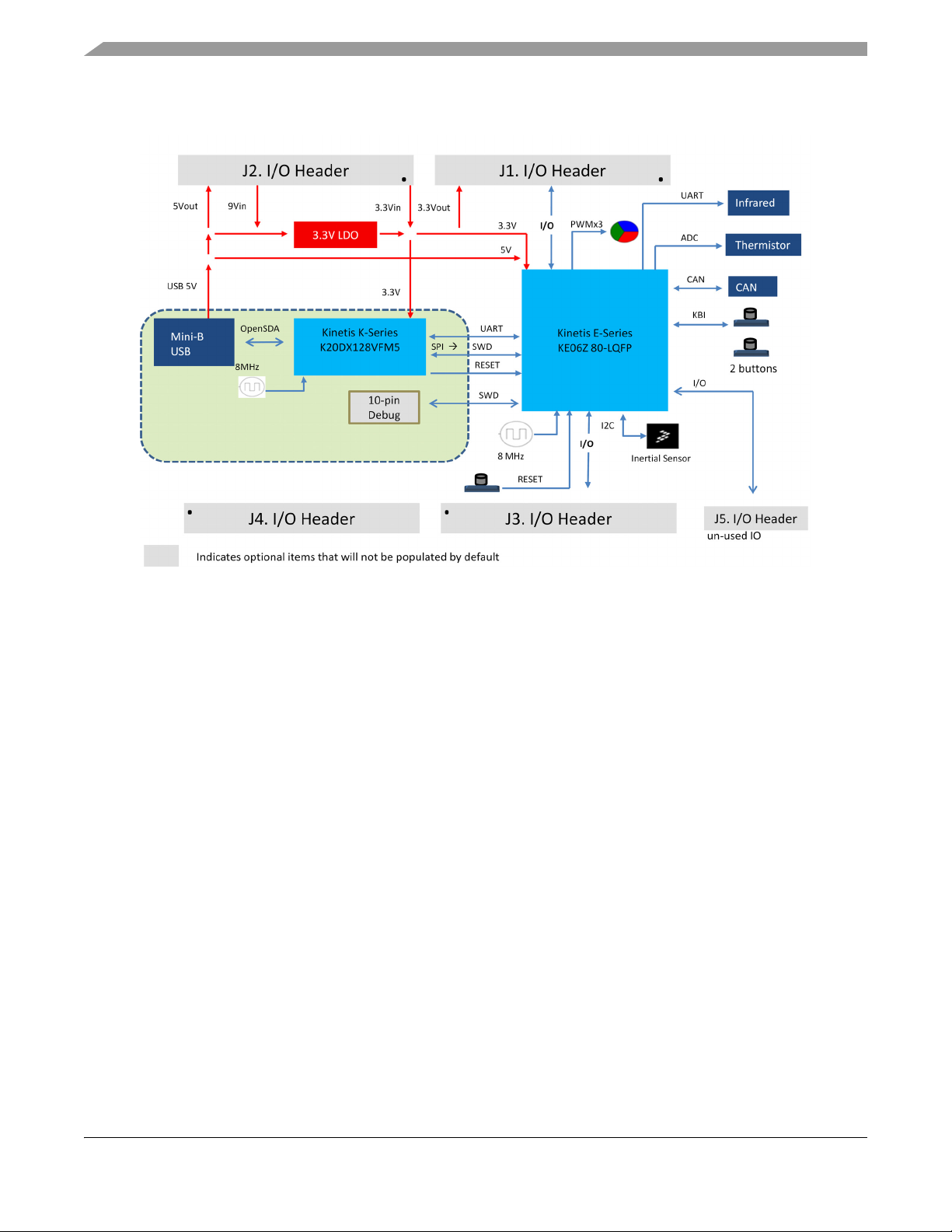
Figure 1 shows a block diagram of the FRDM-KE06 board.
© 2014 Freescale Semiconductor, Inc.
Page 2
FRDM-KE06 hardware description
Figure 1. FRDM-KE06 block diagram
The FRDM-KE06 features two microcontrollers, the target MCU and a serial and debug adapter
(OpenSDA) MCU. The target MCU is a Kinetis E series KE06 family device. The OpenSDA MCU is a
Kinetis K series K20 family device, the K20DX128VFM5.
2 FRDM-KE06 hardware description
2.1 Power supply
The FRDM-KE06 offers a design with multiple power supply options. It can be powered from the USB
connector, the V
header or 3.3V from motor control board. The USB and V
linear regulator to produce the main power supply. The other two sources are not regulated on-board. Note
that KE06 on FRDM board can be powered by 5 V or 3.3 V.
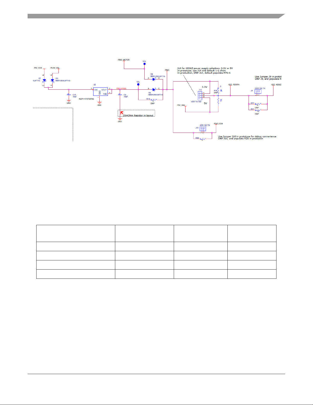
The following figure shows the schematic drawing for the power supply inputs and the on-board voltage
regulator.
pin on the I/O header, an off-board 1.71-3.6V supply from the 3.3V pin on the I/O
IN
supplies are regulated on-board using a 3.3V
IN
FRDMKE06UG, Freedom KE06 User’s Guide, Rev. 0, 03/2014
2 Freescale Semiconductor, Inc.
Page 3
FRDM-KE06 hardware description
Figure 2. FRDM-KE06 power supply
Table 1 provides the operational details and requirements for the power supplies.
Table 1. Power supply requirements
Supply source Valid range OpenSDA operational?
OpenSDA USB (J6) 5V Yes Yes
V
Pin on I/O header 4.3-9V Yes Yes
IN
3.3V Pin on I/O header 1.71-3.6V Yes No
3.3V Pin on motor control header 3.3V Yes No
Regulated
on-board?
Note that the OpenSDA circuit is only operational when a USB cable is connected and supplying power
to J6. However, the protection circuitry is in place to allow multiple sources to be powered at once.
FRDMKE06UG, Freedom KE06 User’s Guide, Rev. 0, 03/2014
Freescale Semiconductor, Inc. 3
Page 4
Serial and Debug Adapter (OpenSDA)
Power supply name Description
VDD_PERIPH Peripheral power supply, including RGB LED, Key buttons, infrared,
VDD_KE06 KE06 MCU power supply.
P3V3_SDA OpenSDA circuit power supply.
Table 2. Power supplies
thermistor, reset circuit.
J14 Pin1&2 connected, 3.3V power supply;
J14 Pin2&3 connected, 5V power supply.
Header J9 provides a convenient means for KE06 energy consumption
measurements.
Header J14 for KE06 power supply selection: 3.3V or 5V.
J14 Pin1&2 connected, 3.3V power supply,
J14 Pin2&3 connected, 5V power supply.
Can be 3.3V only.
Header J10 provides a convenient means for K20 energy consumption
measurements.
P5V_SDA
INPUT
P5-9V_VIN
INPUT
P3V3_MOTOR
INPUT
P5V_USB
OUTPUT
[J6 Pin1] Input 5V Power supplied from the OpenSDA USB connector.
[J4 Pin16] Power supplied from the V
[J2 Pin13] Input 3.3V power supplied from motor control header.
[J4 Pin10] Output 5V to the I/O headers.
Sourced from J6 USB (P5V_SDA) supply through a back drive protection
Schottky diode.
pin of the I/O headers.
IN
Notes:
1. J9 and J10 are not populated by default on the production version. The two pins of these headers
are shorted together by 0 ohm resistor R12 and R26 on the PCB. To measure the energy
consumption of either the KE06 or the OpenSDA MCU, the 0 ohm resistor between these pins
must first be cut. A current probe or a shunt resistor and voltage meter can then be applied to
measure the energy consumption on these rails. When the MCU current measurement is done, this
0 ohm resistor can be soldered on again.
2. To better get ADC accuracy on KE06, it is recommended that a 0 ohm resistor R13 be soldered
on. Ensure there is no power supply from P3V3_MOTOR and P3V3 sourced from I/O headers.
3 Serial and Debug Adapter (OpenSDA)
OpenSDA is an open-standard serial and debug adapter. It bridges serial and debug communications
between a USB host and an embedded target processor as shown in Figure 3.
FRDMKE06UG, Freedom KE06 User’s Guide, Rev. 0, 03/2014
4 Freescale Semiconductor, Inc.
Page 5
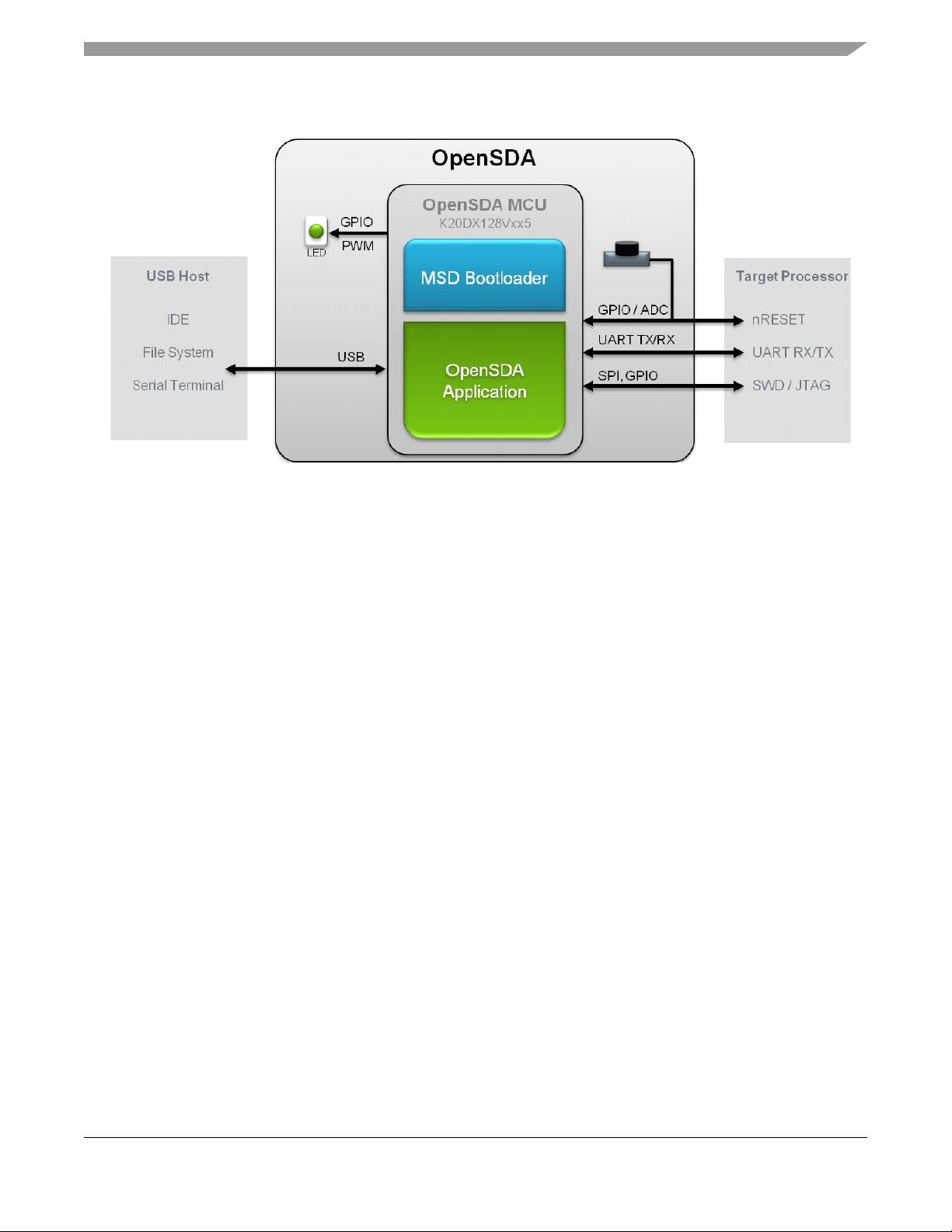
Figure 3. OpenSDA block diagram
Serial and Debug Adapter (OpenSDA)
OpenSDA is managed by a Kinetis K20 MCU built on the ARM® Cortex™-M4 core. The OpenSDA
circuit includes a status LED (D4) and a reset pushbutton (SW1). The pushbutton asserts the reset signal
to the KE06 target MCU. It can also be used to place the OpenSDA circuit into Bootloader mode by
holding down the reset pushbutton while plugging the USB cable to USB connector J6. Once the
OpenSDA enters bootloader mode, other OpenSDA applications such as debug app can be programmed.
SPI and GPIO signals provide an interface to the SWD debug port of the KE06. Additionally, signal
connections are available to implement a UART serial channel. The OpenSDA circuit receives power
when the USB connector J6 is plugged into a USB host.
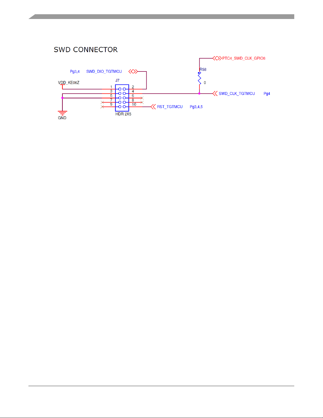
3.1 Debugging interface
Signals with SPI and GPIO capability are used to connect directly to the SWD of the KE06. These signals
are also brought out to a standard 10-pin (0.05”) Cortex Debug connector (J7) as shown in Figure 4. It is
possible to isolate the KE06 MCU from the OpenSDA circuit and use J7 to connect to an off-board MCU.
To accomplish this, cut the 0 ohm resistor R58. This will disconnect the SWD_CLK pin to the KE06 so
that it will not interfere with the communications to an off-board MCU connected to J7.
When KE06 on FRDM board is 5V powered, and the OpenSDA is power off, there need to connect an
external debugger to debug KE06 on board.
FRDMKE06UG, Freedom KE06 User’s Guide, Rev. 0, 03/2014
Freescale Semiconductor, Inc. 5
Page 6
Serial and Debug Adapter (OpenSDA)
Figure 4. SWD debug connector to KE06
3.2 Virtual serial port
A serial port connection is available between the OpenSDA MCU and UART1 pin PTC7 (TXD1) and
PTC6 (RXD1) of KE06. Several of the default OpenSDA applications provided by Freescale, including
the MSD Flash Programmer and the P&E Debug Application, provide a USB Communications Device
Class (CDC) interface that bridges serial communications between the USB host and this serial interface
on the KE06.
3.3 KE06 microcontroller
3.3.1 Clock source
The Kinetis KE06 microcontrollers feature an on-chip oscillator compatible with two ranges of input
crystal or resonator frequencies: 32 kHz (low frequency mode), 4-20 MHz (high frequency mode).
The KE06 on the FRDM-KE06 is clocked from an 8 MHz crystal.
3.3.2 Serial port
The serial port interface signals used with OpenSDA are UART1 pin PTC7 (TXD1) and PTC6 (RXD1).
These signals are also connected to I/O header J1.
3.3.3 Reset
The PTA5/RESET signal on the KE06 is connected externally to a pushbutton SW1. The reset button can
be used to force an external reset event in the target MCU. The reset button can also be used to force the
OpenSDA circuit into bootloader mode when plugging the USB cable to J6. See Section 3, “Serial and
Debug Adapter (OpenSDA)” section for more details.
FRDMKE06UG, Freedom KE06 User’s Guide, Rev. 0, 03/2014
6 Freescale Semiconductor, Inc.
Page 7
Serial and Debug Adapter (OpenSDA)
3.3.4 Debug
The sole debug interface on all Kinetis E Series devices is a Serial Wire Debug (SWD) port. The primary
controller of this interface on the FRDM-KE06 is the onboard OpenSDA circuit. However, a 2x5-pin
(0.05”) Cortex Debug connector, J7, provides access to the SWD signals for the KE06 MCU. The
following table shows SWD connector signals description for KE06:
Table 3. ARM JTAG/SWD mini connector description
Pin Function Connection to KE06
1 VTref 3.3V or 5V KE06 power supply (VDD_KE06)
2 SWDIO/TMS PTA4/SWD_DIO
3GND GND
4 SWDCLK/TCK PTC4/SWD_CLK
5GND GND
6 SWO/TDO NC
7NC NC
8 TDI NC
9NC NC
10 RESET PTA5/RESET
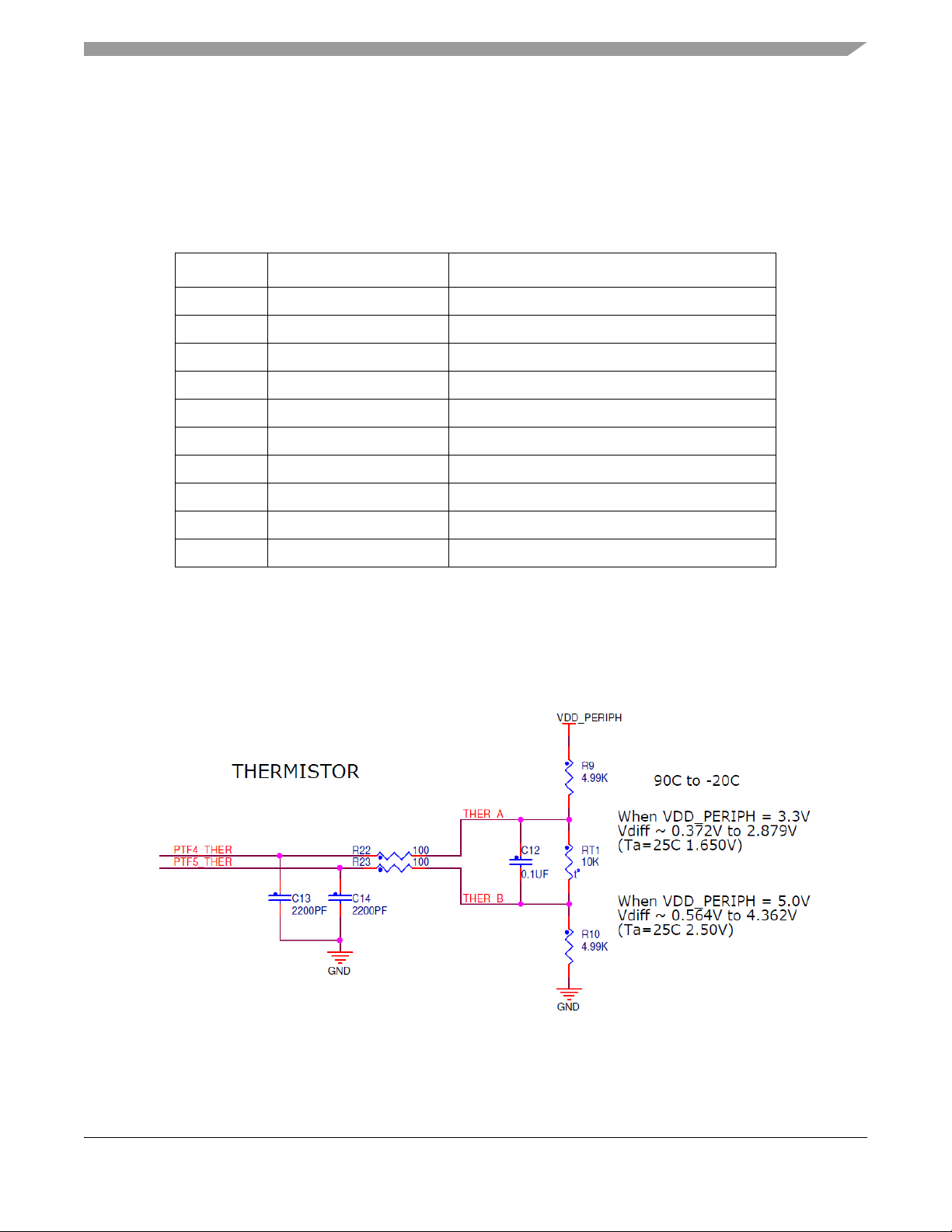
3.4 Thermistor
One thermistor (RT1) is connected to two ADC inputs (PTF4/ADP12, PTF5/ADP13) of KE06 for
evaluating the ADC module.
Figure 5. Thermistor connection
FRDMKE06UG, Freedom KE06 User’s Guide, Rev. 0, 03/2014
Freescale Semiconductor, Inc. 7
Page 8

Serial and Debug Adapter (OpenSDA)
3.5 Infrared port
One infrared Rx port and one Tx port (as shown in the following figure) are connected to ACMP0 input
pin (ACMP0_IN1) and UART0 TXD0 pin of KE06 to demonstrate the capability of SCI0 modulated by a
flextimer to generate infrared signals and use ACMP0 as a filter to receive the SCI data via infrared signal.
Figure 6. Infrared connection
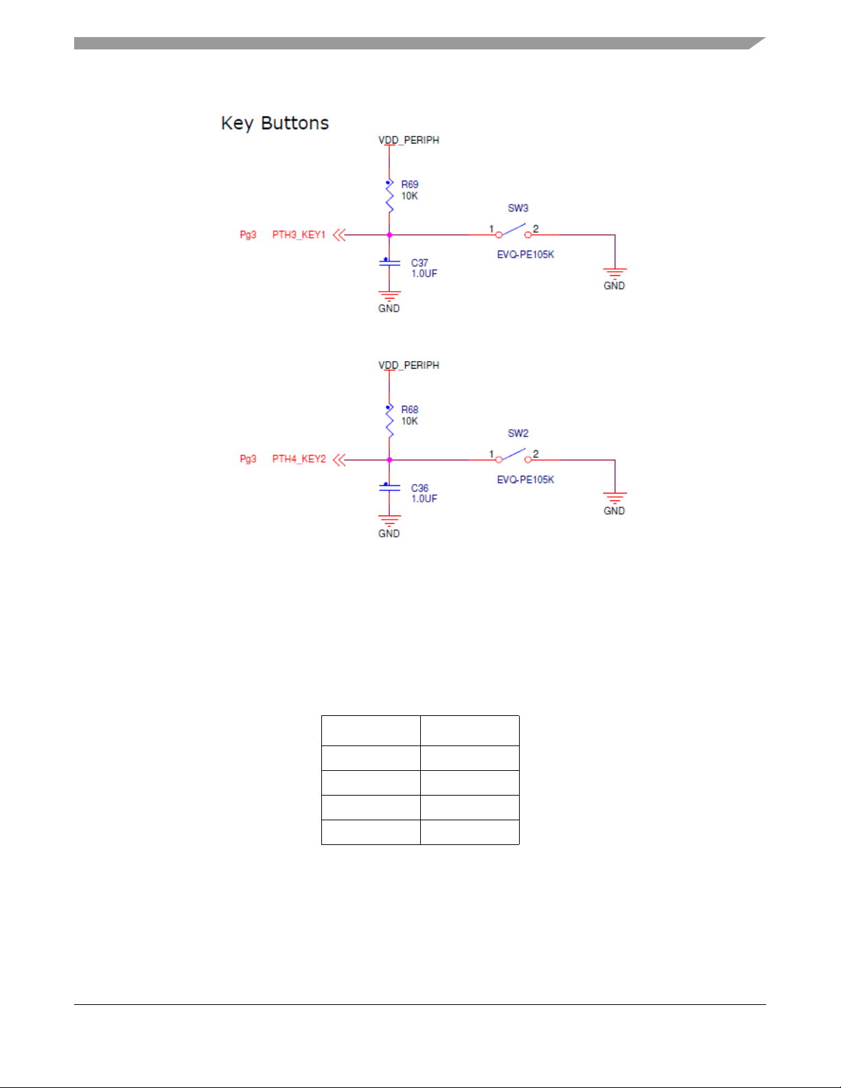
3.6 Key buttons
Two key buttons are connected to PTH3/4 to demonstrate KBI function of KE06, which can capture both
falling edge and rising edge of key button input, as shown in the following figure.
FRDMKE06UG, Freedom KE06 User’s Guide, Rev. 0, 03/2014
8 Freescale Semiconductor, Inc.
Page 9
Serial and Debug Adapter (OpenSDA)
Figure 7. Key buttons connection
3.7 Three-axis accelerometer
A Freescale MMA8451Q low power, three-axis accelerometer is interfaced through an I2C bus and two
GPIO signals as shown in the following table. By default, the I2C address is 0x1D (SA0 pulled high).
Table 4. Accelerometer signal connections
MMA8451Q KE06
SCL PTA3
SDA PTA2
INT1 PTD4
INT2 PTD3
FRDMKE06UG, Freedom KE06 User’s Guide, Rev. 0, 03/2014
Freescale Semiconductor, Inc. 9
Page 10

Serial and Debug Adapter (OpenSDA)
Figure 8. Accelerometer connection
3.8 RGB LED
Three PWM-capable pins are connected to a red, green, blue LED. The signal connections are shown in
the table below.
Table 5. RGB LED Signal Connections
RGB LED KE06
Red Cathode PTG5/FTM2CH3
Green Cathode PTG6/FTM2CH4
Blue Cathode PTG7/FTM2CH5
FRDMKE06UG, Freedom KE06 User’s Guide, Rev. 0, 03/2014
10 Freescale Semiconductor, Inc.
Page 11

Serial and Debug Adapter (OpenSDA)
Figure 9. RGB LED connection
3.9 CAN
The CAN phy on KE06 FRDM board is 3.3 V powered.
Table 6. CAN signal connection
CAN Phy KE06
DCAN_TX
RCAN_RX
FRDMKE06UG, Freedom KE06 User’s Guide, Rev. 0, 03/2014
Freescale Semiconductor, Inc. 11
Page 12

Serial and Debug Adapter (OpenSDA)
Figure 10. CAN
3.10 Input/Output headers
The KE06 microcontroller is packaged in an 80-pin LQFP. Some pins are utilized in on-board circuitry,
but many are directly connected to one of four I/O headers (J1, J2, J3, J4 and J5). J1 and J2 also function
as motor control headers to provide access to a motor control board such as simple BLDC motor driving
board APMOTOR56F8000E.
FRDMKE06UG, Freedom KE06 User’s Guide, Rev. 0, 03/2014
12 Freescale Semiconductor, Inc.
Page 13

Serial and Debug Adapter (OpenSDA)
Figure 11. I/O headers
3.11 Arduino compatibility
The I/O headers on the FRDM-KE06 are arranged to allow compatibility with peripheral boards (known
as shields) that connect to Arduino and Arduino-compatible microcontroller boards. The pins on the
headers share the same mechanical spacing and placement as the I/O headers on the Arduino Uno Revision
3 board design. See Figure 11 for compatible signals.
FRDMKE06UG, Freedom KE06 User’s Guide, Rev. 0, 03/2014
Freescale Semiconductor, Inc. 13
Page 14

How to Reach Us:
Home Page:
freescale.com
Web Support:
freescale.com/support
Information in this document is provided solely to enable system and software
implementers to use Freescale products. There are no express or implied copyright
licenses granted hereunder to design or fabricate any integrated circuits based on the
information in this document.
Freescale reserves the right to make changes without further notice to any products
herein. Freescale makes no warranty, representation, or guarantee regarding the
suitability of its products for any particular purpose, nor does Freescale assume any
liability arising out of the application or use of any product or circuit, and specifically
disclaims any and all liability, including without limitation consequential or incidental
damages. “Typical” parameters that may be provided in Freescale data sheets and/or
specifications can and do vary in different applications, and actual performance may
vary over time. All operating parameters, including “typicals,” must be validated for
each customer application by customer’s technical experts. Freescale does not convey
any license under its patent rights nor the rights of others. Freescale sells products
pursuant to standard terms and conditions of sale, which can be found at the following
address: freescale.com/SalesTermsandConditions.
Freescale, the Freescale logo, and Kinetis are trademarks of Freescale
Semiconductor, Inc., Reg. U.S. Pat. & Tm. Off. All other product or service names are
the property of their respective owners. ARM and Cortex are registered trademarks of
ARM Limited (or its subsidiaries) in the EU and/or elsewhere. All rights reserved.
© 2014 Freescale Semiconductor, Inc.
Document Number: FRDMKE06UG
Rev. 0
03/2014
 Loading...