

Page 1

Service Manual
Model
X-24
multitracker
Page 2
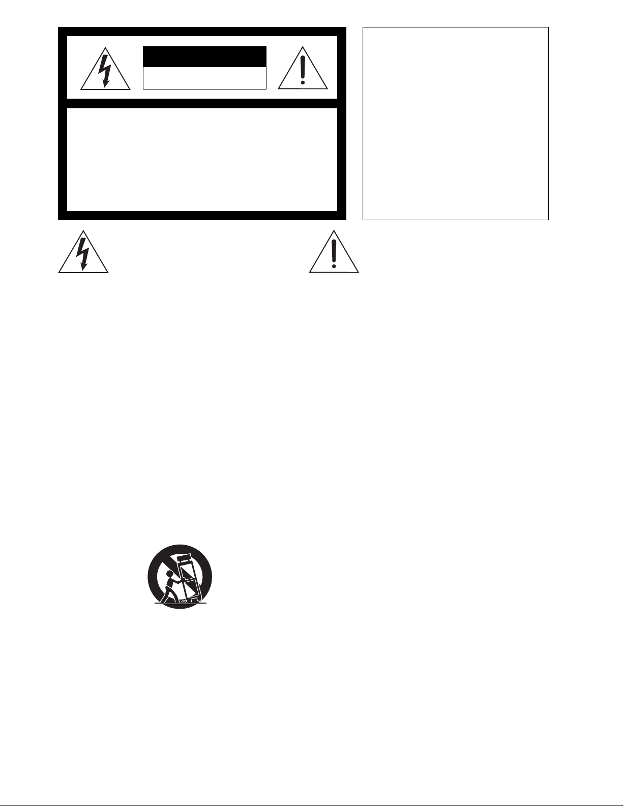
CAUTION
RISK OF ELECTRIC SHOCK
DO NOT OPEN
CAUTION:
TO PREVENT ELECTRIC SHOCK, MATCH
WIDE BLADE OF PLUG TO WIDE SOLT,
FULLY INSERT.
CAUTION: TO REDUCE THE RISK OF ELECTRIC SHOCK,
DO NOT REMOVE COVER (OR BACK).
NO USER-SERVICEABLE PARTS INSIDE.
REFER SERVICING TO QUALIFIED SERVICE PERSONNEL.
The lightening flash with arrowhead symbol,
within an equilateral triangle, is intended to
alert the user to the presence of uninsulated
“dangerous voltage” within the product's enclosure that may be of sufficient magnitude to
constitute a risk of electric shock to persons.
“WARNING”
“TO REDUCE THE RISK OF FIRE OR ELECTRIC SHOCK,
DO NOT EXPOSE THIS APPLIANCE TO RAIN OR MOISTURE.”
SAFETY INSTRUCTIONS
1.
Read instructions - All the safety and operating instructions should be read before the appliance is operated.
2.
Retain instructions - The safety and operating instructions
should be retained for future reference.
3.
Heed warnings - All warnings on the appliance and in the
operating instructions should be adhered to.
4.
Follow instructions - All operating and use instructions
should be followed.
5.
Water and Moisture - The appliance should not be used
near water - for example, near a bathtub, washbowl,
kitchen sink, laundry tub, in a wet basement, or near a
swimming pool, and the like.
6.
Carts and Stands - The appliance should be used only
with a cart or stand that is recommended by the manufacturer.
An appliance and cart combination should be moved with
care. Quick stops, excessive force, and uneven surfaces
may cause the appliance and cart combination to overturn.
Wall or Ceiling Mounting - The appliance should be
7.
mounted to a wall or ceiling only as recommended by the
manufacturer.
Ventilation - The appliance should be situated so that its
8.
location or position does not interfere with its proper ventilation. For example, the appliance should not be situated on a bed, sofa, rug, or similar surface that may block
the ventilation openings; or, placed in a built-in installation, such as a bookcase or cabinet that may impede the
flow of air through the ventilation openings.
ATTENTION:
POUR ÉVITER LES CHOCS ÉLECTRIQUES,
INTRODUIRE LA LAME LA PLUS LARGE DE
LA FICHE DANS LA BORNE CORRESPONDANTE DE LA PRISE ET POUSSER
JUSQU' AU FOND.
The exclamation point within an equilateral
triangle is intended to alert the user to the
presence of important operating and maintenance (servicing) instructions in the literature
accompanying the appliance.
Heat - The appliance should be situated away from heat
9.
sources such as radiators, heat registers, stoves, or other
appliances (including amplifiers) that produce heat.
Power Sources - The appliance should be connected to a
10.
power supply only of the type described in the operating
instructions or as marked on the appliance.
Grounding or Polarization - The precautions that should
11.
be taken so that the grounding or polarization means of
an appliance is not defeated.
Power Cord Protection - Power supply cords should be
12.
routed so that they are not likely to be walked on or
pinched by items placed upon or against them, paying
particular attention to cords at plugs, convenience receptacles, and the point where they exit from the appliance.
Cleaning - The appliance should be cleaned only as rec-
13.
ommended by the manufacturer.
Nonuse Periods - The power cord of the appliance should
14.
be unplugged from the outlet when left unused for a long
period of time.
Object and Liquid Entry - Care should be taken so that
15.
objects do not fall and liquids are not spilled into the enclosure through openings.
Damage requiring Service - The appliance should be ser-
16.
viced by qualified service personnel when:
The power supply cord or the plug has been damaged;
A.
or
Objects have fallen, or liquid has been spilled into the
B.
appliance; or
The appliance has been exposed to rain; or
C.
The appliance does not appear to operate normally or
D.
exhibits a marked changed in performance; or
The appliance has been dropped, or the enclosure
E.
damaged.
Servicing - The user should not attempt to service the ap-
17.
pliance beyond that described in the operating instructions. All other servicing should be referred to qualified
service personnel.
Page 3

TABLE OF CONTENTS
X-24
1. SPECIFICATIONS . . . . . . . . . . . . . . . . . . . . . . . . . . . . . . . . . . . . . . .
2. CONTROLS, INDICATORS AND CONNECTORS . . . . . . . . . . . .
3. ADJUSTING PROCEDURES . . . . . . . . . . . . . . . . . . . . . . . . .
4. EXPLODED VIEW, PCB ASSEMBLY AND PARTS LIST . . . . . .
5. CIRCUIT & BLOCK DIAGRAMS . . . . . . . . . . . . . . . . . . . . . . . .
4
7
8
14
23
NOTES
Adjusting Procedures, Parts List and circuit diagrams are given in this manual to assist the service technician in
*
maintaining the Model X-24.
The following accessories are supplied with X-24 as the standard accessories.*
Owner's manual : 8288418000 (for export & domestic model)
AC adaptor AD-12A : 8270727003 (for USA/CND)
!
: 8270727006 (for EUR)
: 8270727007 (for UK)
: 8270727010 (for JPN)
Following is the packing material for the Model X-24.
*
Carton, inner, X-24 : 8228715000
Packing, L, X-24 : 8228439001
Packing, R, X-24 : 8228439002
CAUTION
Parts marked with this sign are safety critical components. They must always be replaced with identical components.
!
Refer to the Fostex Parts List and ensure exact replacement.
3
Page 4

X-24
1. SPECIFICATIONS
DEFINITION
Specification Unit 0 dBV = 1 Vrms
Normal Fader Position
Input fader At 8 ± 1 position
Condition LINE IN / INSERT: -10 dBV / 1 kHz
Recorder: Input Monitor mode (REC - PAUSE)
Adjust input fader for -10 dBV at TAPE OUT.
PAN: L (R)
Master fader At 8 ± 1 position
Condition LINE IN / INSERT: -10 dBV / 1 kHz
Recorder: Input Monitor mode (STOP)
Adjust master fader for -10 dBV at LINE OUT.
PAN: L (R)
MIXER SECTION
Standard Input
MIC IN
Connector Phone (unbalanced) / XLR (balanced)
Input level -50 ~ -10 dBV
Impedance 10 kΩ or more
LINE IN / INSERT (RCV)
Connector Stereo phone (tip)
Input level -10 dBV
Impedance 10 kΩ or more
Standard Output
TAPE OUT 1 ~ 4
Connector RCA pin
Output level -10 dBV
Load impedance 10 kΩ or more
LINE OUT L, R
Connector RCA pin
Output level -10 dBV
Load impedance 10 kΩ or more
INSERT (SEND)
Connector Stereo phone (ring)
Output level -10 dBV
Load impedance 10 kΩ or more
Phones Max. Output Level 20 mW or more (1 kHz, 16 Ω load)
Level Indication 0 dB is indicated by 5-dot LED bargraph meter when input / output
level is -10 dBV with the above standard input / master fader
position settings.
Frequency Response
MIC IN (Input Level: -50 dBV) 40 ~ 20 kHz ± 3 dB at LINE OUT
MIC IN (Input Level: -10 dBV) 20 ~ 20 kHz ± 3 dB at LINE OUT
LINE IN (Input Level: -10 dBV) 50 ~ 10 kHz ± 2 dB at PHONES (10 mW / 16 Ω)
S / N (shorted by 150
MIC IN (MIC GAIN: MIC) 66 dB or more at LINE OUT (DIN AUDIO)
MIC IN (MIC GAIN: LINE) 73 dB or more at LINE OUT (DIN AUDIO)
ΩΩ
Ω resistor)
ΩΩ
68 dB or more at LINE OUT (IHF A)
75 dB or more at LINE OUT (IHF A)
4
Page 5
MIXER SECTION (continued)
Distortion
(With 400 Hz HPF & 30 kHz LPF) 0.05 % or less (Input: 1 kHz / 0 dBV signal, MIC GAIN: LINE, LINE
OUT: 0 dBV.)
0.2 % or less (Input: 1 kHz / 0 dBV signal, MIC GAIN:LINE,
PHONES: 3 mW / 16Ω.)
Fader Attenuation 70 dB or more at 1 kHz (from standard fader position)
Crosstalk 60 dB or more at 1 kHz (Input: MIC IN, MIC GAIN: LINE, OUT: SEND
OUT. Measure level at non-input channel.)
PAN Crosstalk 42 dB or more at 1 kHz (Input: MIC IN, MIC GAIN: LINE, OUT: LINE
OUT. Measure level at non-input channel.)
Click Noise
Power on / off -20 dBVp-p or less
Other switching -30 dBVp-p or less
Shock Noise -30 dBVp-p or less (Measure noise level when one side of appliance is
dropped 3 times from 5 cm height.)
RECORDER SECTION
Tape Speed 9.5 cm/s ± 1.5 % (3000 Hz ± 45 Hz when reproducing TCW-211 test
tape.)
Wow & Flutter
PLAY 0.25 % or less (TCW-211 test tape, ANSI WTD.)
REC & PLAY 0.30 % or less (AC-514 test tape, ANSI WTD.)
Pitch Control
MIN (PITCH VR: Fully CCW) -45 % or less (TCW-211 test tape)
MAX (PITCH VR: Fully CW) +12 % or more (TCW-211 test tape)
Fast Winding Time (FF / RWD) 150 ± 20 sec. (TAPE: C-60)
Tape Counter Deviation 0 ± 7 (FF from BOT to EOT and then RWD to BOT again.)
Standard Level
PLAY -10 ± 1 dB (TCW-231 test tape)
REC & PLAY -10 ± 1 dBV (AC-514 test tape, 1 dB or less of level difference between
channels is also required.)
Frequency response
PLAY Test tape: SCW-977 / TCW-284F (NR: OUT)
X-24
+3 dB
-3 dB
400 Hz 12.5 kHz40 Hz
REC & PLAY Test tape: AC-514 (NR: OUT, recording level: 0 dB)
+3 dB
-3 dB
400 Hz 12.5 kHz40 Hz
Test tape: AC-514 (NR: IN, recording level: -25dB)
5 dB
250 Hz
10 kHz
6 dB
12.5 kHz
5
Page 6

X-24
RECORDER SECTION (continued)
Level Deviation at Reference Output Level
PLAY 1 dB or less at 400 Hz (NR: OUT, TCW-231 test tape)
3 dB or less at 40 HZ ~ 12.5 kHz (NR: OUT, SCW-977 /
TCW-284F test tape)
REC & PLAY 1 dB or less at 400 Hz (NR: OUT, AC-514 test tape)
2 dB or less at 100 Hz ~ 10 kHz (NR: OUT, AC-514 test tape)
S/N
PLAY 47 dB or more (NR: OUT, DIN AUDIO)
55 dB or more (NR: OUT, IHF-A)
REC & PLAY 45 dB or more (NR: OUT, DIN AUDIO)
48 dB or more (NR: OUT, IHF-A)
48 dB or more (NR: IN, DIN AUDIO)
55 dB or more (NR: IN, IHF-A)
Distortion (REC & PLAY) 2 % or less (Input signal: 1 kHz / standard level, standard fader position,
with 400 Hz HPF & 30 kHz LPF)
Erasure Ratio 67 dB or more at 1 kHz (Input signal: 1 kHz / 0 dBV, standardfader
position, with 1 kHz BPF)
Cross Erasure 1 dB or less (Input signal: 10 kHz / -10 dBV, standard fader position.
Measure level difference when adjacent track is put into REC mode.)
Channel Separation 50 dB or more (Input signal: 1 kHz / -10 dBV, standard fader position,
with 1 kHz BPF. Measure leakage level when adjacent track is put into
REC mode.)
Sync Crosstalk -25 dBV or less (Input signal: 1 kHz / -10 dBV)
-10 dBV or less (Input signal: peak frequency / -10 dBV)
(Measure leakage level when adjacent track is put into REC mode.)
Bias Leakage -35 dBV or less (No LED meter is lit. Standard fader position.
Measure leakage level at TAPE OUT when unit is put into REC mode.)
Click Noise
→→
PLAY
→ STOP -30 dBVp-p or less
→→
→→
REC
→ STOP
→→
Monitor -20 dBVp-p or less
PLAY -20 dBVp-p or less
Punch In / Out -30 dBVp-p or less at PLAY
Shock Noise -30 dBVp-p or less (Measure playback noise level when one side of
appliance is dropped 3 times from 5 cm height.)
Specifications and appearance are subject to change without notice for product improvement.
6
Page 7
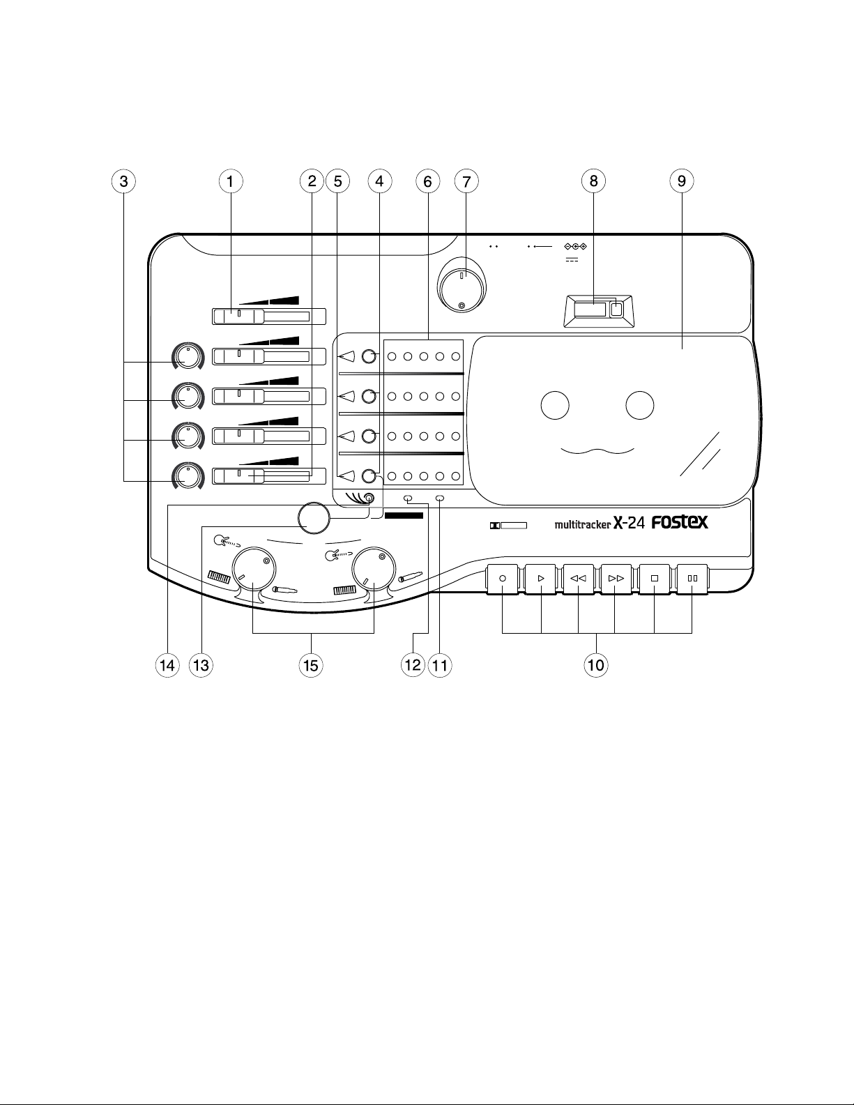
2. CONTROLS, INDICATORS & CONNECTORS
< Top Panel >
X-24
MASTER
PAN INPUT/PLAYBACK LEVEL
1
L
R
2
R
L
3
R
L
4
LR
1/3
Auto
Bounce
MIC IN
REC SEL
1
REC SEL
2
REC SEL
3
REC SEL
4
RL4321
LINE OUTLINE IN/INSERT
REHEARSAL
2/4
OFF ON
DOLBY NR
-+
WIDE PITCH
6+305-10
6+305-10
6+305-10
6+305-10
POWERREC
STANDBY
DOLBY B NR
REC REW FF STOP PAUSEPLAY
ON
DC IN
12V
RESET
000
1. Master fader [MASTER
]
2. Input/playback level control faders
[
INPUT/PLAYBACK LEVEL
3. Pan pot knob [PAN
]
]
4. Record track select switches [REC SEL
5. Record track LED
6. Level meter
7. Pitch control knob [WIDE PITCH
8. Tape counter/reset button [RESET
]
]
9. Cassette lid/Cassette tray
10.Transport control buttons
Play button [PLAY
Stop button [STOP
Fast forward button [FF
]
Rewind button [REW
Recording button [REC
Pause button [PAUSE
11. Power LED [POWER
12. Record LED [REC
13. Auto bounce on/off button [Auto Bounce
]
]
]
]
]
]
]
]
]
14. Auto bounce LED
15. Trim knob
7
Page 8
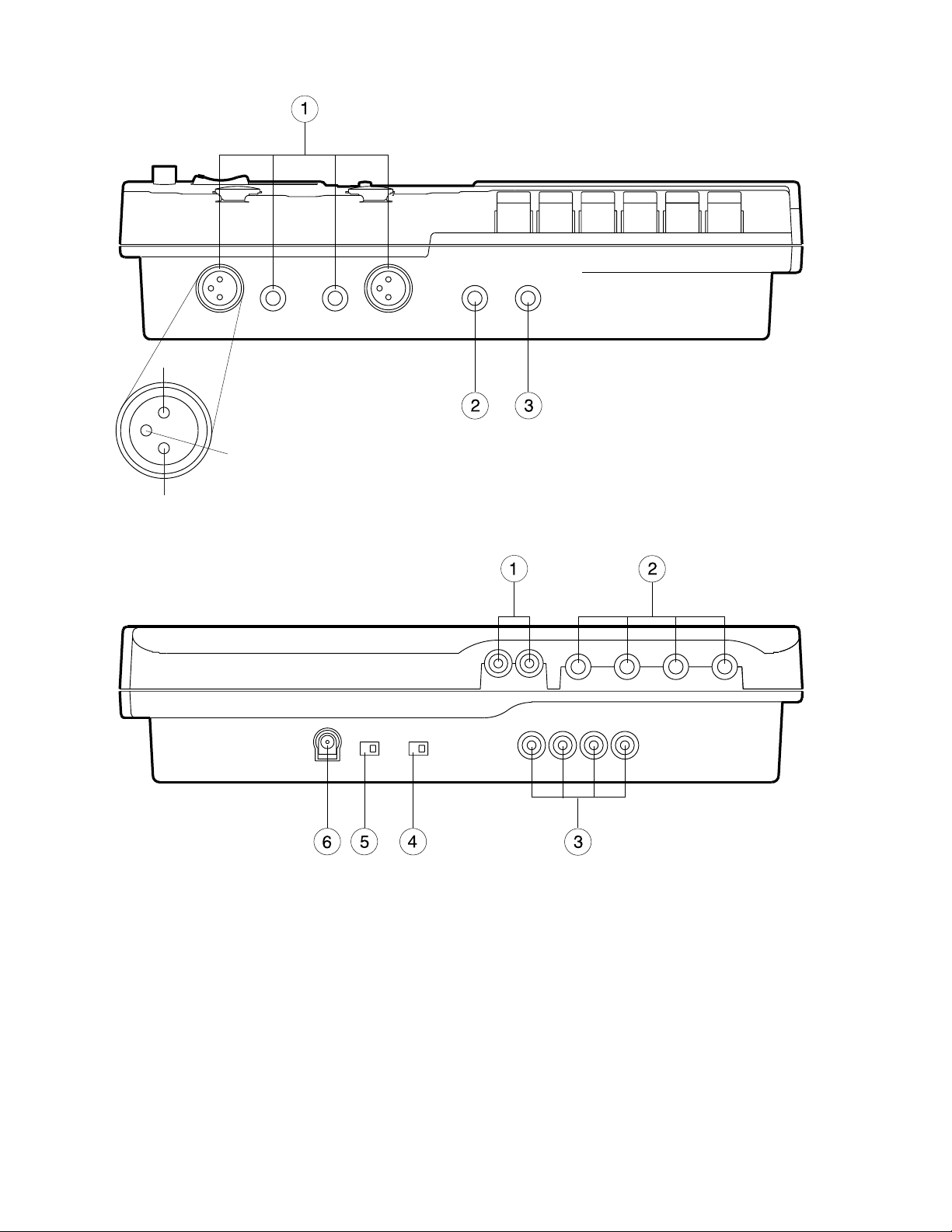
X-24
< Front Panel >
)
2 (HOT
PUNCH
IN/OUTPHONES
)
1 (GND
3 (COLD
)
< Rear Panel >
1. Line out jacks [LINE OUT L, R
2. Line in/insert jacks [LINE/INSERT 1, 2, 3, 4
3. Tape out jacks [TAPE OUT 1, 2, 3, 4
]
]
1. Mic input jacks [MIC IN 1/3, 2/4
2. Headphone jack [PHONES
3. Punch in/out jack [PUNCH IN/OUT
TAPE OUT
1234
]
]
]
4. Dolby B noise reduction on/off switch
]
[
DOLBY NR ON/OFF
]
5. Power switch [ON-STANDBY
6. DC IN connector [DC IN 12V
]
]
3. ADJUSTING PROCEDURES
3-1. Routine Maintenance
3-1-1. Cleaning
1) Head
With constant use, the head surface becomes soiled with magnetic particles from the tape, dirt and dust. Under such
conditions, the tape will not always be in smooth contact with the head and thus result in poor performance. Less
8
Page 9

output in the high region and dropout (some parts of sound not reproduced) are typical symptoms. It is therefore
recommended to clean the heads periodically before recording and playback to avoid such troubles.
2) Capstan and pinch roller
Buildup of magnetic particles and dust on these parts will cause increase in wow, flutter and wrapping of tape on
the capstan. Thus, these parts must always be kept clean. Cleaning is done with cotton buds moistened with fluids
prescribed or recommended for tape recorders and especially the heads. Never use lacquer thinner, acetone or
other organic solvents.
3-1-2. Demagnetizing
The REC/PLAY head becomes magnetized by extended use or when the head is touched with a magnetized object.
As a result, frequency response especially in the high region will deteriorate, noise level increases, and in some
cases may transfer noise to valuable prerecorded tapes. For this reason, do not touch the head with magnetized
screwdriver and scissors or allow DC current to flow through the head winding such as when testing continuity
with a circuit tester. Should the head becomes magnetized, demagnetize it with a head demagnetizer designed for
this purpose.
Demagnetizing Procedures
After turning off the power of Model X-24, open the cassette lid and if a cassette tape is loaded, remove and place
1)
it far away from the deck.
Switch on the head demagnetizer while holding it about one meter away from the Model X-24. Then, slowly move
2)
the head demagnetizer tip to the head and wave the tip up and down several times close to the head surface.
On completing the above procedures, slowly draw the demagnetizer away from the head and switch it off when it
3)
is more than one meter away from the head. As demagnetizm in the head cannot be seen, unlike the soiled head,
routine demagnetizing is necessary. It is recommended to do so at the same time the head is cleaned.
X-24
3-2. Test Equipment and Adjusting Tools
The following tools and equipment are required for adjusting the Model X-24.
1)
Head height and tape contact adjusting jig Model 9001 (P/N: 8286001000)
2)
Torque meter
Cassette torque meter TW-2231 (P/N: 8286008000): 0 ~ 200 g-cm (0 ~ 2.8 Oz-In)
Cassette torque meter TW-2111A (P/N: 8286009000): 0 ~ 100 g-cm (0 ~ 1.4 Oz-In)
3)
Mirror tape cassette TCC-902 (P/N: 8286002000)
4)
Test tape
Speed / Flutter (3 kHz) Model 9152 (P/N: 82660022000)
Also 3150 Hz test tape for Wow & Flutter measurement is
recommended.
Reference playback level TCW-231 (P/N: 8266002000)
Playback frequency response TCW-284F (P/N: 8266003000)
5)
Blank tape C-90 or shorter tape, TYPE II / HIGH position
6)
Audio oscillator General type
7)
Frequency counter General type
8)
Bandpass filter General type
9)
AC voltmeter Stereo type is recommended.
10)
Oscilloscope General type
11)
Wow & Flutter meter General type
12)
Distortion meter General type
13)
Frequency counter General type
9
Page 10

X-24
3-3. Tape Transport Mechanical Data
3-3-1. Reel torque
PLAY mode (TW-2111A) Supply: 1.5 ~ 6 g-cm
1)
Takeup: 20 ~ 70 g-cm
FF/REW mode (TW-2231) FF /REW: 60 ~ 120 g-cm
2)
3-3-2. Pinch roller pressure
Pull force 300 ~ 500 g
3-4. Tape Travel Check and Adjustment
Using the mirror type cassette, check to see that the tape is running stable between the ERASE and REC/PLAY
heads tape guides without weaving. If the tape is not running stable between the guides, erasure and frequency
response will be affected or the tape will be damaged by curling. It then becomes necessary to check the guide
height, perpendicularity of the head surface, and alignment of the pinch roller in relation to the capstan. In addition
to the mirror type cassette, the Head Height and Tape Contact Jig is required. To check the head guide height, the
cassette tape is removed and the above jig is placed on the head mount base plate. While firmly seating the jig on
the base plate surface, slide the jig past each head guide to see that it goes through without hitting them. Also check
perpendicularity of each head surface, using the rear check bar of the jig. If the guide is low, insert the required
amount of 0.1 mm or 0.2 mm thick washers under the head mounting legs, or vice versa, if it is high.
NOTE: Always adjust the head azimuth and phase when the head height is adjusted.
3-5. Volume & SW setting
Input fader At 8 ± 1 position
Master fader At 8 ± 1 position
Pan Fully CCW (L) or CW (R) position
3-6. Check and Adjusting of Head Azimuth
Switch off the DOLBY SW.
1)
Connect an AC volt meter to the TAPE OUT and playback the 12.5 kHz section on the TC-284W test tape.
2)
Rotate the REC/PLAY head azimuth adjusting screw to obtain a maximum output level.
3)
3-7. Tape Speed Check and Adjustment
Confirm that the Pitch control knob is at center position.
1)
Connect a frequency counter or wow & flutter meter with frequency counter to the TAPE OUT and playback the
2)
Model 9152 test tape.
Check the tape speed and wow & flutter if they satisfy the following specifications.
3)
Tape Speed: 3000 Hz ± 30 Hz at both BOT (beginning of tape) and EOT (end of tape) positions
Wow & Flutter: 0.25 % (CCIR WTD) at both BOT and EOT positions
If the tape speed is not within the above specification, adjust R43 (3.3 kΩ) on the R/P AMP PCB assy.
4)
Next, check if the tape speed variable range satisfies the specifications below.
5)
Maximum tape speed: +12 % or more (3360 Hz or more)
Minimum tape speed: -45 % or less (1650 Hz or less)
10
3-8. Playback Level Calibration
Set the controls as follows.
1)
Record track select switch: OFF
Dolby B noise reduction on/off switch: OFF
Connect an AC volt meter to the TAPE OUT 1 through 4 pin jacks.
2)
Page 11

Playback the TCW-231 test tape and check the output level if it is -10 dBV (0.3 V) ± 1 dB reading.
3)
If the reading is not within the above range, adjust R106 ~ R406 on the R/P AMP PCB assy.
4)
3-9. Playback Frequency Response Calibration
Set the controls as follows.
1)
Record track select switch: OFF
Dolby B noise reduction on/off switch: OFF
Connect an AC volt meter to the TAPE OUT 1 through 4 pin jacks respectively.
2)
Playback the TCW-284F test tape and adjust R103 ~ R403 so that the output level at 6.3 kHz is 0.5 dB lower than
3)
the 400 Hz output level.
Confirm that the output level at 12.5 kHz is within ± 1 dB of the 400 Hz output level.
4)
3-10. Erase Current Adjustment
At adjusting the erase current, put a blank cassette tape to the transport and the track to be adjusted is put in REC mode.
Assuming the track 1 to be adjusted, the oscilloscope probe is connected to the test point TP106 on the R/P PCB assy
and rotate and fix the core T101 for minimum voltage point. Then, confirm that the voltage at TP105 is more than 55 mV.
X-24
NOTE:
Adjust the remaining tracks in the same way.
If the voltage at TP106 is adjusted at minimum, the erase current flowing the erase head is set to the maximum.
Track 2:
Track 3:
Track 4:
Adjust T201 for minimum voltage at TP206. Then, confirm that the voltage at TP205 is more than 55 mV.
Adjust T301 for minimum voltage at TP306. Then, confirm that the voltage at TP305 is more than 55 mV.
Adjust T401 for minimum voltage at TP406. Then, confirm that the voltage at TP405 is more than 55 mV.
3-11. Coarse Bias Adjustment
At coarsely adjusting the bias current, put a blank cassette tape to the transport and the track to be adjusted is put
in REC mode. Assuming the track 1 to be adjusted, the oscilloscope probe is connected to the test point TP104 on
the R/P PCB assy and rotate and fix the pot R133 (220 kΩ) at 60 mV.
Adjust the remaining tracks in the same way.
Track 2:
Track 3:
Track 4:
Adjust R233 so that the voltage at TP204 is 60 mV.
Adjust R333 so that the voltage at TP304 is 60 mV.
Adjust R433 so that the voltage at TP404 is 60 mV.
3-12. Record Level Calibration
The procedures up to 3-10 must be completed before proceeding to this adjustment.*
Put a blank cassette tape to the transport and apply a 400 Hz, -10 dBV (0.3 V) sine wave signal to the INPUT 1 and
1)
2 phone jacks. (In the case the signal is input from XLR jack, the terminal No.3 (COLD) and No. 1 (GND) must be
shortened.)
Set the controls as follows.
2)
Record track select switch: All tracks ON (Confirm that the REC TRK LEDs (1 ~ 4) are blinking.)
Trim knob: At minimum
Dolby B noise reduction on/off switch: OFF
Connect an AC volt meter to the TAPE OUT 1 ~ 4 pin jacks.
3)
Put the transport into REC PAUSE mode and adjust the Input Fader so that the level at TAPE OUT 1 ~ 4 is -10 dBV
4)
(0.3 V).
Release the PAUSE button and start recording the signal.
5)
After recording a certain length, rewind the tape to the start point of recording section. Then, playback the tape and
6)
check the level at TAPE OUT 1 ~ 4. If the AC volt meter reading is not within -10 dBV (0.3 V) ± 0.5 dB, adjust the
pot R121 ~ 421 (22 kΩ) on the R/P PCB assy.
11
Page 12

X-24
3-13. Overall Frequency Response Adjustment
Set the controls under the same condition as 3.12 except the DOLBY switch. (The switch should be turned on.)
1)
Apply a 400 Hz, -35 dBV (18 mV) signal to the INPUT 1 and 2 phone jacks.
2)
Record the signal, rewind and playback the recorded section of the tape and memorize the output level at TAPE
3)
OUT 1 ~ 4.
Next, apply 6 kHz & 12 kHz, -35 dBV (18 mV) signals to the INPUT 1 and 2 phone jacks.
4)
Record the signal, rewind and playback the recorded section of the tape.
5)
Check if the 6 kHz / 12 kHz output level at TAPE OUT 1 ~ 4 is within ± 2 dB comparing to the 400 Hz output level.
6)
If the AC volt meter reading is not within the above specification, adjust the pot R133 ~ 433 (220 kΩ) on the R/P
AMP PCB assy so that the recording level at 6 kHz will be within the specification.
3-14. T.H.D. Measurement
Connect a distortion meter, 400 Hz HPF and 30 kHz LPF to TAPE OUT 1 ~ 4 and set the controls under the same
1)
condition as 3-12.
Record a 1 kHz, -10 dBV (0.3 V) sine wave signal.
2)
Playback the recorded part and check if the distortion level is less than 2 %.
3)
3-15. Erasure Measurement
Connect a 1 kHz bandpass filter and AC volt meter to TAPE OUT 1 ~ 4 and set the controls under the same
1)
condition as 3-12.
Record a 1 kHz, 0 dBV (1 V) sine wave signal which is 10 dB higher than the reference recording level on a blank
2)
tape.
Rewind the tape to the start point of recording and advance it by a short length. Then, record again without
3)
applying the signal on the remaining part.
Rewind the tape to the start point again and play it back. Check if the level ratio between the playback level and no-
4)
signal section (erased part) is 67 dB or more.
3-16. Cross Erasure Measurement
Set the controls as follow.
1)
Trim knob: At minimum
Input fader: Standard position (At 8 ± 1)
Dolby B noise reduction on/off switch: OFF
Input a 100 kHz, -10 dBV signal to the INPUT 1 and 2 phone jacks and record the signal on all tracks.
2)
Rewind the tape to the start point of recording. Then, erase the 10 kHz signal on the track and check if the level
3)
difference at the corresponding track indicated below is within 1 dB.
Tracks to be measured Track (s) to be erased
12
2 1 and 3
3 2 and 4
43
If the level goes down by more than 1 dB, check the tape running path again.
4)
12
Page 13

3-17. Sync crosstalk measurement
Sync crosstalk is a relative figure against the reference level, on how much of the recording signal from a track in
recording mode is leaking into the track being reproduced. When sync crosstalk is excessively high, playback output
during overdubbing will sound muddy by effect of the recording signal leakage or cause oscillation at pingpong
recording (where the playback output is transferred to another track).
Set the controls as follow and put a blank tape to the transport.
1)
Trim knob: At minimum
Input fader: Standard position (At 8 ± 1)
Dolby B noise reduction on/off switch: OFF
Apply a signal whose level is -10 dBV (0.3 V).
2)
Put one track into REC mode and check if the level at TAPE OUT on an adjacent track is within the specifications
3)
listed below when sweeping the oscillator frequency.
At 1 kHz: -25 dBV or less
1 ~ 20 kHz: -10 dBV or less
3-18. S/N Measurement
3-18-1. Reproduce
Set the control as follow.
1)
Dolby B noise reduction on/off switch: OFF
Connect an AC volt meter and put the transport into PLAY mode without loading a tape.
2)
Check if the AC volt meter reading is within the following specifications.
3)
DIN AUDIO: 47 dB
IHF-A: 55 dB
X-24
3-18-2. Record and reproduce (Overall)
Set the control as follow.
1)
Dolby B noise reduction on/off switch: OFF
Put a blank cassette tape and start recording without applying a signal.
2)
Rewind the tape to the start point and play it back.
3)
Check if the AC volt meter reading is within the following specifications.
4)
DIN AUDIO: 45 dB
IHF-A: 48 dB
Next, turn the Dolby switch on and repeat the above procedures 2) ~ 4).
5)
Check if the AC volt meter reading is within the following specifications.
6)
DIN AUDIO: 48 dB
IHF-A: 55 dB
3-19. Click Noise Measurement
3-19-1. Dolby switch on/off
Check if the click noise level at TAPE OUT when turning on/off the Dolby switch is less than -30 dBVp-p.1)
3-19-2. REC/STOP (monitor)
Check if the click noise level at TAPE OUT when punching out by pressing the STOP button is less than -20 dBVp-p.1)
3-19-3. REC/STOP (on tape)
Turn off the Dolby switch, turn on all the 1 ~ 4 record track switches and put a blank cassette tape in the transport.
1)
Plug the foot switch (e.g. Model 8051) in the Punch in/out jack and press the PLAY button.
2)
Press the foot switch repeatedly and check if the click level at TAPE OUT 1 ~ 4 is less than -20 dBVp-p.
3)
13
Page 14

X-24
3-20. Table of Adjusting Items
Adjusting Item Measuring Point Adjusting Point Ref. Clause (page)
Tape speed TAPE OUT R43 (R/P) 3-7 ( P10)
Playback level calibration TAPE OUT 1 ~ 4 R106 ~ R406 (R/P) 3-8 (P10 ~ 11)
Playback frequency response calibration TAPE OUT 1 ~ 4 R103 ~ R403 (R/P) 3- 9 (P11)
Erase c urrent adjustment 3-10 ( P11)
Coarse bias adjustment TP104 ~ 404 R133 ~ 433 3-11 (P11)
Record level calibr ati on TAPE OUT 1 ~ 4 R121 ~ 421 3-12 (P11)
Overall frequency response adjustment TAPE OUT 1 ~ 4 R133 ~ 433 3-13 (P12)
TP106 ~ TP406 T101 ~ 401 (R/P)
TP105 ~ TP405
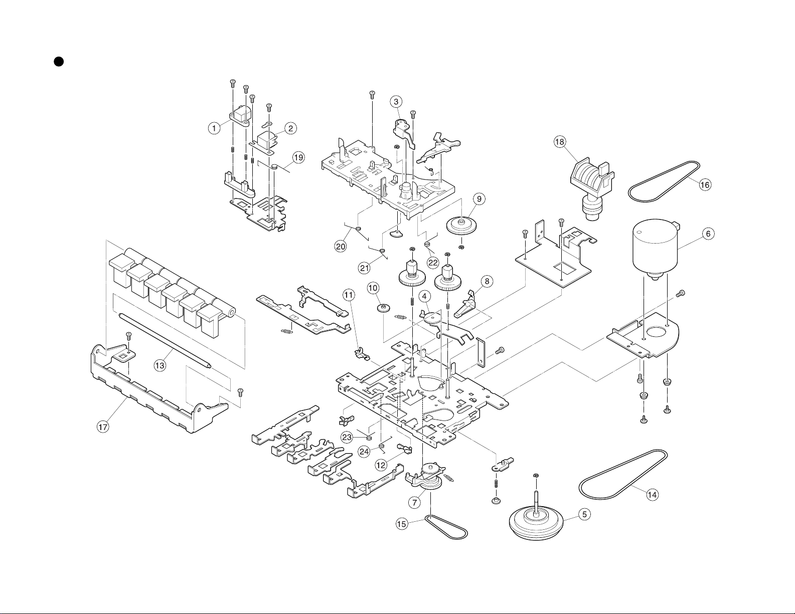
4. EXPLODED VIEW, PCB ASSEMBLY AND PARTS LIST
X-24 OVERALL EXPLODED VIEW & PARTS LIST
Ref. No. Part No. Description
1 8216 6580 00 Sheet, meter, X-24
2 8212 5931 00 Cover, cassette, X-14/24
3 8212 6050 00 Case, top, X-24
4 8226 1590 04 Knob, fader, N7, GR
5 8226 1590 05 Knob, fader, N7, R
6 8226 2070 02 Knob, pitch, gain, N7
7 8226 2070 01 Knob, pitch, N7
8 8216 6490 00 Cushion, cover, X-14/24
9 8216 4230 00 Reflector, cassette
10 8214 2110 00 Spring, cassette, X-18/14/24
11 8216 6590 00 Shield, top, X-24
12 8226 2360 01 Knob, sel, bounce, X-24
13 8204 0370 01 Ring, CSTW-2
14 8226 1620 05 Knob, volume, N7, Y
15 8274 1330 00 PCB assy, Mixer, X-24
16 8216 6610 00 Shield, bottom, X-24
17 8270 8240 00 Transport assy, X-24
18 8226 2131 01 Knob, cassette, REC, X-14/24
19 8226 2101 01 Knob, cassette, PLAY, X-14/24
Ref. No. Part No. Description
20 8226 2091 01 Knob, cassette, REW, X-14/24
21 8226 2081 01 Knob, cassette, FF, X-14/24
22 8226 2111 01 Knob, cassette, STOP, X-14/24
23 8226 2121 01 Knob, cassette, PAUSE, X-14/24
24 8216 6600 00 Shield, center, X-24
25 8274 1340 00 PCB assy, Jack, X-24
26 8221 2260 00 Bracket, jack, X-24
!
27 8274 1350 00 PCB assy, R/P, X-24
28 8204 0820 00 Plate, mounting, B
29 8212 6060 00 Case, bottom, X-24
!
30 8270 7270 03 AC adaptor, AD-12A, USA/CND
8270 7270 06 AC adaptor, AD-12A, EUR
8270 7270 07 AC adaptor, AD-12A, UK
8270 7270 10 AC adaptor, AD-12A, JPN
31 8274 1400 00 PCB assy, Regulator, X-24
!
32 8216 6800 00 Sheet, isolation X-24
33 8277 4470 15 Cable assy, 1P, earth lug, D3-8MF/F,
L150
14
X-24 TRANSPORT EXPLODED VIEW & PARTS LIST
Ref. No. Part No. Description
1 8259 0500 00 Head, erase, X-14/24
2 8259 0520 00 Head, R/P, 4T, N-LR44RS07, X-24
3 8260 4620 00 Pinch roller assy
4 8260 4630 00 Idler arm assy
5 8260 4640 00 Fly wheel assy
6 8260 4650 00 Motor assy
7 8260 4660 00 F.R. arm assy
8 8212 4930 00 Lever, REC safety
9 8212 4910 00 Gear, arm
10 8212 4920 00 Gear, FF
11 8253 4280 00 SW, leaf, MSW-1541XACV
12 8253 4290 00 SW, leaf, MSW-1716CV
Ref. No. Part No. Description
13 8223 2770 00 Shaft, button
14 8216 5310 00 Belt, main
15 8216 5320 00 Belt, sub
16 8216 5330 00 Belt, counter
17 8221 1970 00 Bracket, button
18 8256 1690 00 Counter
19 8214 3550 00 Spring, pinch arm
20 8214 3560 00 Spring, FR torsion
21 8214 3570 00 Spring, stop/pause
22 8214 3580 00 Spring, safety sensor
23 8214 3590 00 Spring, rec lever
24 8214 3600 00 Spring, play lever
Page 15

X-24 OVERALL EXPLODED VIEW
1
5
6
4
8
7
9
BBT 3x8 CZn
X-24
2
BBT 3x8 CZn
17
3
18
19
10
20
21
22
23
11
13
12
BBT 3x8 CZn
3x8 CZn
14
BBT
33
BBT 3x8 CZn
26
31
BBT 3x8 CZn
24
BBT 3x8 CZn
25
16
BBT 3x8 CZn
32
30
BBT 3x8 CZn
28
27
BBT 3x8 CZn
29
15
BBT 3x12 BZn
15
Page 16
16
X-24
X-24 TRANSPORT EXPLODED VIEW
Page 17
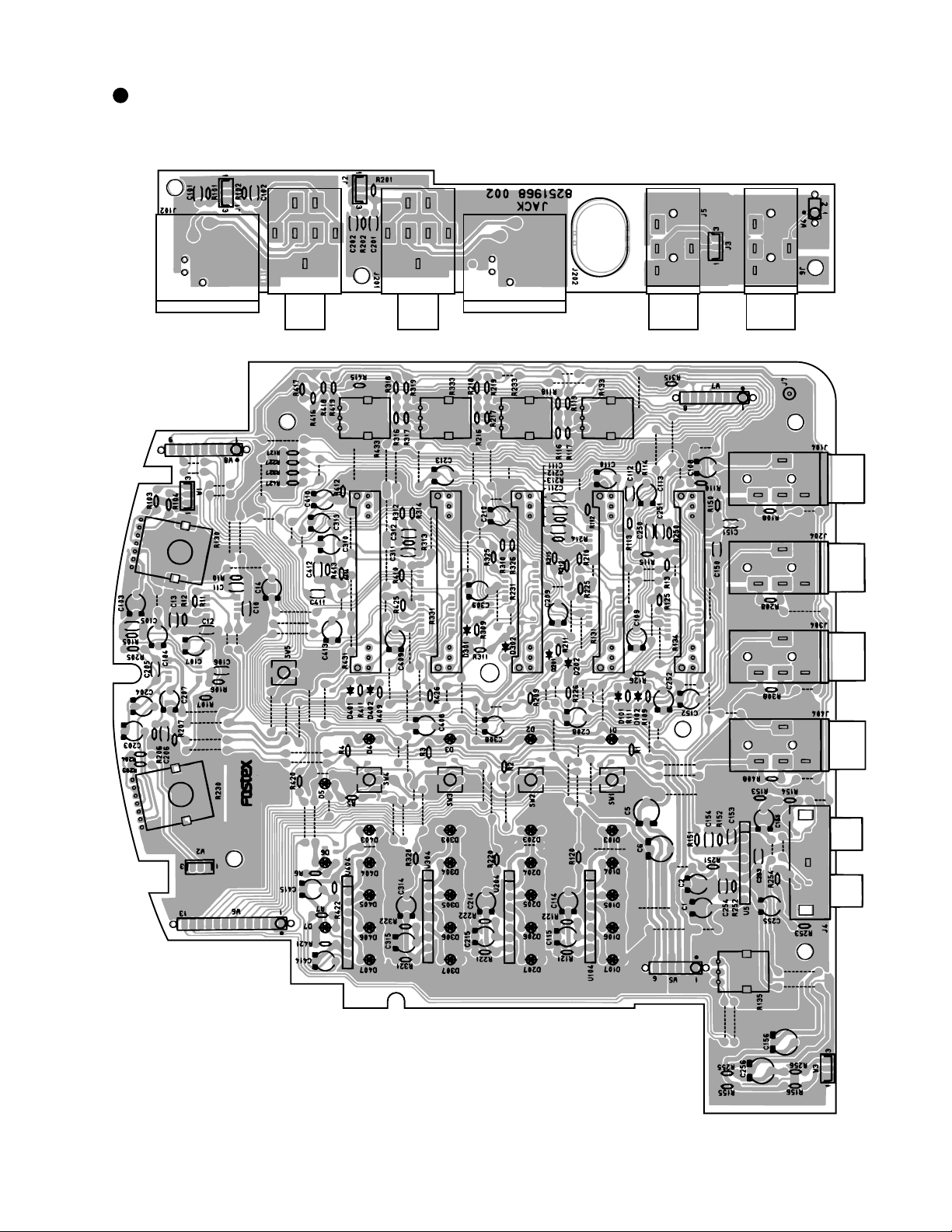
X-24 PCB PATTERN DRAWING
X-24
• MIXER / JACK PCBs
17
Page 18
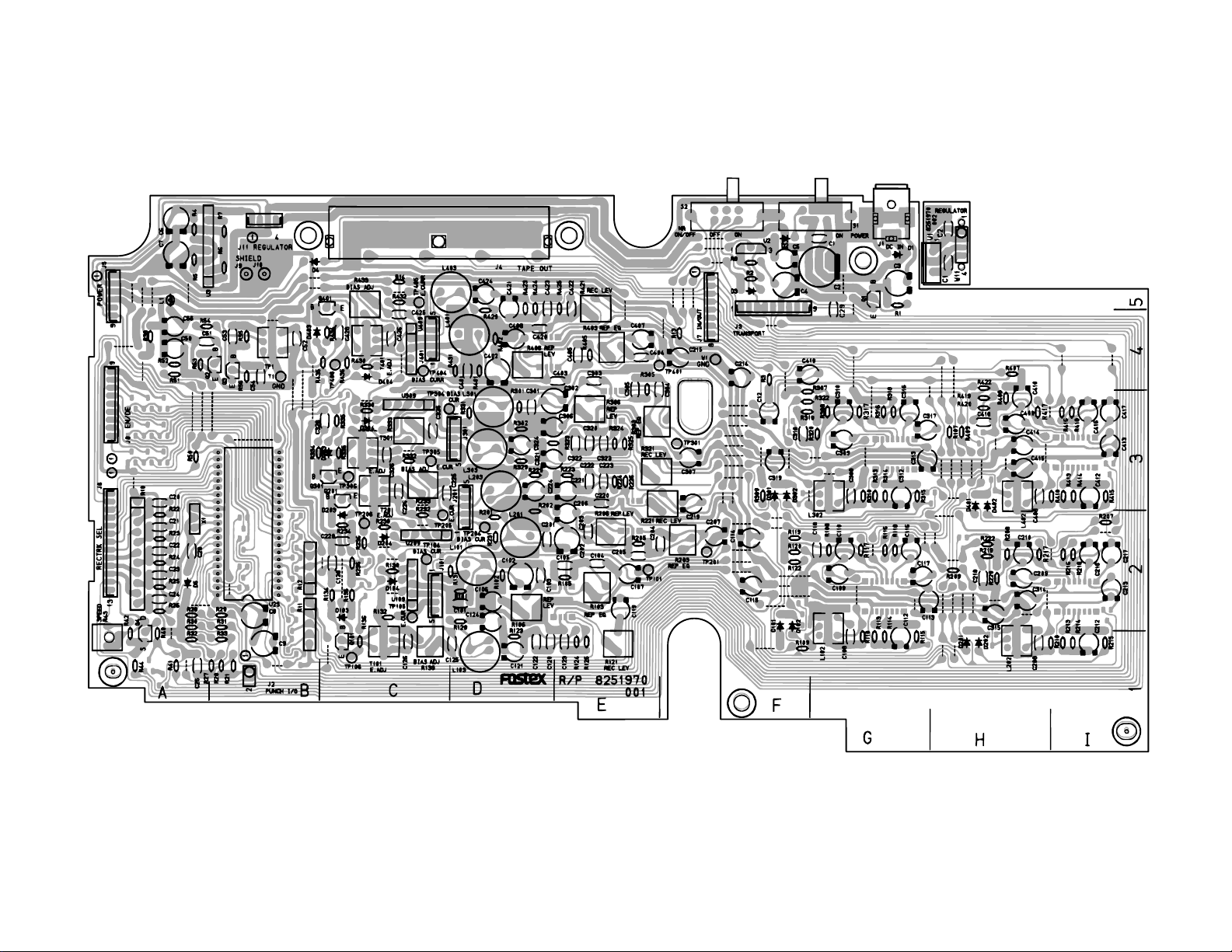
18
X-24
• R/P / REGULATOR PCBs
Page 19

X-24 Parts List
• MIXER PCB
Ref. No. Part No. Description
8274 1330 00 PCB assy, Mixer, X-24
B001 8251 9680 01 Plain PCB, Mixer, X-24
ICs
Ref. No. Part No. Description
U001 8236 5405 00 ST, analog, NJM2068M
U002~004 8236 7207 00 ST, analog, NJM4560M
U005 8236 0352 03 SIP, analog, NJM4556AL
U006 8236 7207 00 ST, analog, NJM4560M
U007~012 8236 5707 01 ST, digital, DTA144EK
U101~401 8236 5000 00 ST, digital, CMOS, 4066BF
U102~402 8236 5706 01 ST, digital, DTC144EK
U103~403 8236 5706 01 ST, digital, DTC144EK
U104~404 8236 0832 00 SIP, analog, LED driver, BA6124
U105~205 8236 5702 01 ST, digital, driver, DTC314TK
DIODEs
Ref. No. Part No. Description
D001~005 8234 1046 02 Opt., VT, LED, GRN,
SLR-332MC-TE7
D006 8234 1046 01 Opt., VT, LED, RED,
SLR-332VC-TE7
D007 8234 1046 02 Opt., VT, LED, GRN,
SLR-332MC-TE7
D101~401 8234 5007 00 HT, 1SS136
D102~402 8234 5007 00 HT, 1SS136
D103~403 8234 1046 03 Opt., VT, LED, YEL,
SLR-332YC-TE7
D104~404 8234 1046 03 Opt., VT, LED, YEL,
SLR-332YC-TE7
D105~405 8234 1046 03 Opt., VT, LED, YEL,
SLR-332YC-TE7
D106~406 8234 1046 01 Opt., VT, LED, RED,
SLR-332VC-TE7
D107~407 8234 1046 01 Opt., VT, LED, RED,
SLR-332VC-TE7
RESISTORs
Ref. No. Part No. Description
R001~007 8230 1387 51 HT, carbon, 1/4W, 750Ω, 5%
R010~012 8230 1381 23 HT, carbon, 1/4W, 12kΩ, 5%
R013 8230 1384 73 HT, carbon, 1/4W, 47kΩ, 5%
R103, 203 8230 1381 02 HT, carbon, 1/4W, 1kΩ, 5%
R104, 204 8230 1381 02 HT, carbon, 1/4W, 1kΩ, 5%
R105, 205 8230 1381 04 HT, carbon, 1/4W, 100kΩ, 5%
R106, 206 8230 1381 04 HT, carbon, 1/4W, 100kΩ, 5%
R107, 207 8230 1384 73 HT, carbon, 1/4W, 47kΩ, 5%
X-24
Ref. No. Part No. Description
R108~408 8230 1384 32 HT, carbon, 1/4W, 4.3k Ω, 5%
R109~409 8230 1383 03 HT, carbon, 1/4W, 30kΩ, 5%
R110~410 8230 1384 73 HT, carbon, 1/4W, 47kΩ, 5%
R111~411 8230 1381 23 HT, carbon, 1/4W, 12kΩ, 5%
R112~412 8230 1381 04 HT, carbon, 1/4W, 100kΩ, 5%
R113~413 8230 1381 23 HT, carbon, 1/4W, 12kΩ, 5%
R114~414 8230 1381 23 HT, carbon, 1/4W, 12kΩ, 5%
R115~415 8230 1384 73 HT, carbon, 1/4W, 47kΩ, 5%
R116~416 8230 1382 43 HT, carbon, 1/4W, 24kΩ, 5%
R117~417 8230 1382 43 HT, carbon, 1/4W, 24kΩ, 5%
R118~418 8230 1383 03 HT, carbon, 1/4W, 30kΩ, 5%
R119~419 8230 1383 03 HT, carbon, 1/4W, 30kΩ, 5%
R120~420 8230 1381 23 HT, carbon, 1/4W, 12kΩ, 5%
R121~421 8230 1385 12 HT, carbon, 1/4W, 5.1k Ω, 5%
R122~422 8230 1381 03 HT, carbon, 1/4W, 10kΩ, 5%
R125~425 8230 1384 73 HT, carbon, 1/4W, 47kΩ, 5%
R126~426 8230 1381 23 HT, carbon, 1/4W, 12kΩ, 5%
R127~427 8230 1381 23 HT, carbon, 1/4W, 12kΩ, 5%
R130, 230 8240 1710 28 Pot, PI, RT14, 100kΩCC,
RK14K123, L15
R131 8240 2740 03 Pot, PI, SL30, 20kΩA, RS30H111
R133~433 8240 1670 06 Pot, PI, RT09, 50kΩB, RK09K113
R134~434 8240 2740 04 Pot, PI, SL30, 20kΩAA, RS30H121
R135 8240 1670 08 Pot, PI, RT09, 10kΩB, RK09K113
R150, 250 8230 1386 83 HT, carbon, 1/4W, 68kΩ, 5%
R151, 250 8230 1381 23 HT, carbon, 1/4W, 12kΩ, 5%
R152, 252 8230 1382 43 HT, carbon, 1/4W, 24kΩ, 5%
R153, 253 8230 1384 73 HT, carbon, 1/4W, 47kΩ, 5%
R154, 254 8230 1381 02 HT, carbon, 1/4W, 1kΩ, 5%
R155, 255 8230 1384 73 HT, carbon, 1/4W, 47kΩ, 5%
R156, 256 8230 1381 60 HT, carbon, 1/4W, 16Ω, 5%
CAPACITORs
ALU = Electrolytic type
CER = Ceramic type
Ref. No. Part No. Description
C001, 002 8232 1424 76 VT, ALU, 10V, 47µF, 20%, SME
C005, 006 8232 1424 76 VT, ALU, 10V, 47µF, 20%, SME
C010 8232 8012 21 VT, CER, 50V, 220pF, 5%, SL
C011 8232 8012 20 VT, CER, 50V, 22pF, 5%, SL
C012 8232 8012 21 VT, CER, 50V, 220pF, 5%, SL
C013 8232 8012 20 VT, CER, 50V, 22pF, 5%, SL
C014 8232 1431 06 VT, ALU, 16V, 10µF, 20%, SME
C103, 203 8232 1421 07 VT, ALU, 10V, 100µF, 20%, SME
C104, 204 8232 1421 07 VT, ALU, 10V, 100µF, 20%, SME
C105, 205 8232 8011 00 VT, CER, 50V, 10pF, 5%, SL
C106, 206 8232 8011 00 VT, CER, 50V, 10pF, 5%, SL
19
Page 20

X-24
Ref. No. Part No. Description
C107, 207 8232 1431 06 VT, ALU, 16V, 10µF, 20%, SME
C108~408 8232 1431 06 VT, ALU, 16V, 10µF, 20%, SME
C109~409 8232 1431 06 VT, ALU, 16V, 10µF, 20%, SME
C110~410 Wire, jumper, IPS-1041-2, F5
C111~411 N/A
C112~412 N/A
C113~413 8232 1431 06 VT, ALU, 16V, 10µF, 20%, SME
C114~414 8232 1431 06 VT, ALU, 16V, 10µF, 20%, SME
C115~415 8232 1431 06 VT, ALU, 16V, 10µF, 20%, SME
C150, 250 8232 8012 21 VT, CER, 50V, 220pF, 5%, SL
C151, 251 8232 8012 20 VT, CER, 50V, 22pF, 5%, SL
C152, 252 8232 1431 06 VT, ALU, 16V, 10µF, 20%, SME
C153, 253 8232 8012 21 VT, CER, 50V, 220pF, 5%, SL
C154, 254 8232 8012 20 VT, CER, 50V, 22pF, 5%, SL
C155, 255 8232 1431 06 VT, ALU, 16V, 10µF, 20%, SME
C156, 256 8232 1424 77 VT, ALU, 10V, 470µF, 20%, SME
MISCELLANEOUS
Ref. No. Part No. Description
E001 Wire, jumper, IPS-1041-2, F5
E002 Wire, jumper, IPS-1041-4, F10
J004 8245 2120 01 Connector, PL, jack, RCA, 2P, BLK
J007 8245 5280 01 Connector, PI, jack, 1P, RT-01T-1.0B
J104~404 8245 2980 00 Connector, PL, jack, phone,
LGR4609-7000
S001~005 8253 1350 02 Switch, PT, tact, SOR-112HS
Y005 8207 0122 09 Holder, cable, 9P, 51048
Y006 8207 0122 13 Holder, cable, 13P, 51048
Y007 8207 0122 08 Holder, cable, 8P, 51048
Y008 8207 0122 06 Holder, cable, 6P, 51048
W001 8277 0160 15 Cable assy, shield 2C, 3P,
WHT-9073, L150
W002 8277 0161 30 Cable assy, shield 2C, 3P,
RED-9073, L300
W003 8277 0162 50 Cable assy, shield 2C, 3P,
BLK-9073, L500
W005 8276 9086 25 Cable, flat, 6P, L250
W006 8276 9093 25 Cable, flat, 13P, L250
W007 8276 9088 25 Cable, flat, 8P, L250
W008 8276 9089 25 Cable, flat, 9P, L250
• JACK PCB
Ref. No. Part No. Description
8274 1340 00 PCB assy, Mixer, X-24
B001 8251 9681 02 Plain PCB, Jack, X-24
Ref. No. Part No. Description
R102, 202 8230 1381 23 Resistor, HT, carbon, 1/4W,
12kΩ, 5%
C101, 201 N/A
C102, 202 N/A
E001 Wire, jumper, IPS-1041-2, F5
E002 Wire, jumper, IPS-1041-4, F10
J001 8245 1711 03 Connector, PI, jack, 8283, 3P, WHT
J002 8245 1712 03 Connector, PI, jack, 8283, 3P, RED
J003 8245 1713 03 Connector, PI, jack, 8283, 3P, BLK
J005 8245 2980 00 Connector, PL, jack, phone,
LGR4609-7000
J006 8245 2980 00 Connector, PL, jack, phone,
LGR4609-7000
J101, 201 8245 3390 04 Connector, PL, jack, phone,
YKB21-5074
J102, 202 8245 2680 04 Connector, PL, jack, XLR31,
NC3FAHR10
W004 8276 9082 20 Cable, flat, 2P, L200
Y901 8207 0122 02 Holder, cable, 2P, 51048
• R/P PCB
Ref. No. Part No. Description
8274 1350 00 PCB assy, R/P, X-24
B001 8251 9700 01 Plain PCB, R/P, X-24
ICs
Ref. No. Part No. Description
U001 N/A
U002 8236 0782 06 PT, digital, driver, DTA143TS
U003 8236 0361 00 SIP, analog, BA4560N
U004~022 8236 5707 01 ST, digital, driver, DTA144EK
U023 8236 0837 00 SDI, digital, CPU, X-24,
TMP47C200BN
U030, 031 8236 5706 01 ST, digital, driver, DTC144EK
U040 8236 5706 01 ST, digital, driver, DTC144EK
U041 8236 5707 01 ST, digital, driver, DTA144EK
U101~401 8236 5405 00 ST, analog, NJM2068M
U102~402 8236 0457 00 SOP, analog, HA12135AF
U104~404 8236 5701 03 ST, digital, driver, DTC114TK
U105~405 8236 5707 01 ST, digital, driver, DTA144EK
U106~406 8236 5701 03 ST, digital, driver, DTC114TK
U107~407 8236 5701 03 ST, digital, driver, DTC114TK
U108~408 8236 5701 03 ST, digital, driver, DTC114TK
U109~409 8236 4190 00 SIP, analog, head SW, BA7755A
20
Ref. No. Part No. Description
R101, 201 8230 1381 23 Resistor, HT, carbon, 1/4W,
12kΩ, 5%
TRANSISTORs
Ref. No. Part No. Description
Q001 8234 1430 00 V, NPN, 2SC3071
Page 21

X-24
Ref. No. Part No. Description
Q002, 003 8234 5043 03 VT, NPN, 2SC1740S, S
Q004 8234 5050 00 VT, FET, 2SK117, Y/GR/BL
Q101~401 8234 5043 03 VT, NPN, 2SC1740S, S
DIODEs
Ref. No. Part No. Description
D001 8234 0196 02 VT, DSK10C-BT
D002 Wire, jumper, IPS-1041-2, F5
D003 8234 0196 02 VT, DSK10C-BT
D004, 005 8234 5007 00 HT, 1SS136
D101~401 8234 5007 00 HT, 1SS136
D102~402 8234 5007 00 HT, 1SS136
D103~403 8234 5007 00 HT, 1SS136
D104~404 8234 5007 00 HT, 1SS136
RESISTORs
Ref. No. Part No. Description
R001 8230 1388 21 HT, carbon, 1/4W, 820Ω, 5%
R002 8230 1383 94 HT, carbon, 1/4W, 390kΩ, 5%
R003 8230 1382 03 HT, carbon, 1/4W, 20kΩ, 5%
R004, 005 8230 1381 03 HT, carbon, 1/4W, 10kΩ, 5%
R006. 007 8230 1382 20 HT, carbon, 1/4W, 22Ω, 5%
R008 8230 1387 51 HT, carbon, 1/4W, 750Ω, 5%
R010 8230 0510 06 V, array, 1/8W, 47kΩ-47kΩ x 5,
5%, RKC-E
R011 8230 0361 03 V, array, 1/8W, 10kΩ x 4, 5%, RKC
R012 8230 0361 03 V, array, 1/8W, 10kΩ x 4, 5%, RKC
R013, 014 8230 1384 79 HT, carbon, 1/4W, 4.7Ω, 5%
R020 8230 1384 73 HT, carbon, 1/4W, 47kΩ, 5%
R021 8230 1381 03 HT, carbon, 1/4W, 10kΩ, 5%
R022~026 8230 1384 73 HT, carbon, 1/4W, 47kΩ, 5%
R027 8230 1381 03 HT, carbon, 1/4W, 10kΩ, 5%
R028, 029 8230 1384 73 HT, carbon, 1/4W, 47kΩ, 5%
R030 8230 1381 03 HT, carbon, 1/4W, 10kΩ, 5%
R031 8230 1384 73 HT, carbon, 1/4W, 47kΩ, 5%
R032 8230 1381 03 HT, carbon, 1/4W, 10kΩ, 5%
R033 8230 1384 73 HT, carbon, 1/4W, 47kΩ, 5%
R038 8230 1381 03 HT, carbon, 1/4W, 10kΩ, 5%
R040 8230 1381 05 HT, carbon, 1/4W, 1MΩ, 5%
R041 8230 1381 03 HT, carbon, 1/4W, 10kΩ, 5%
R042 8230 1383 32 HT, carbon, 1/4W, 3.3kΩ, 5%
R043 8231 5033 32 R-TRIM, PIT, carbon, 3.3kΩ, 637T
R044 8230 1385 11 HT, carbon, 1/4W, 510Ω, 5%
R050 8230 1382 03 HT, carbon, 1/4W, 20kΩ, 5%
R051 8230 1384 72 HT, carbon, 1/4W, 4.7kΩ, 5%
R052 8230 1383 32 HT, carbon, 1/4W, 3.3kΩ, 5%
R053 8230 1384 73 HT, carbon, 1/4W, 47kΩ, 5%
R054 8230 1384 70 HT, carbon, 1/4W, 47Ω, 5%
R055 8230 1383 33 HT, carbon, 1/4W, 33kΩ, 5%
R056 8230 1384 72 HT, carbon, 1/4W, 4.7kΩ, 5%
R101~401 8230 1382 43 HT, carbon, 1/4W, 24kΩ, 5%
Ref. No. Part No. Description
R102~402 8230 1381 04 HT, carbon, 1/4W, 100kΩ, 5%
R103~403 8231 5032 23 R-TRIM, PIT, carbon, 22kΩ, 637T
R105~405 8230 1383 94 HT, carbon, 1/4W, 390kΩ, 5%
R106~406 8231 5034 71 R-TRIM, PIT, carbon, 470Ω, 637T
R107~407 8230 1383 32 HT, carbon, 1/4W, 3.3k Ω, 5%
R108~408 8230 1381 81 HT, carbon, 1/4W, 180Ω, 5%
R109~409 8230 1382 22 HT, carbon, 1/4W, 2.2k Ω, 5%
R110~410 8230 1383 32 HT, carbon, 1/4W, 3.3k Ω, 5%
R113~413 8230 1381 83 HT, carbon, 1/4W, 18kΩ, 5%
R114~414 8230 1382 03 HT, carbon, 1/4W, 20kΩ, 5%
R115~415 8230 1382 03 HT, carbon, 1/4W, 20kΩ, 5%
R116~416 8230 1382 41 HT, carbon, 1/4W, 240Ω, 5%
R117~417 8230 1382 02 HT, carbon, 1/4W, 2kΩ, 5%
R118~418 8230 1382 02 HT, carbon, 1/4W, 2kΩ, 5%
R119~419 8230 1382 02 HT, carbon, 1/4W, 2kΩ, 5%
R120~420 8230 1384 72 HT, carbon, 1/4W, 4.7k Ω, 5%
R121~421 8231 5032 23 R-TRIM, PIT, carbon, 22kΩ, 637T
R122~422 8230 1386 22 HT, carbon, 1/4W, 6.2k Ω, 5%
R123~423 8230 1383 63 HT, carbon, 1/4W, 36kΩ, 5%
R124~424 8230 1381 53 HT, carbon, 1/4W, 15kΩ, 5%
R125~425 8230 1381 53 HT, carbon, 1/4W, 15kΩ, 5%
R129~429 8230 1386 22 HT, carbon, 1/4W, 6.2k Ω, 5%
R130~430 8230 1381 03 HT, carbon, 1/4W, 10kΩ, 5%
R131~431 8230 1381 01 HT, carbon, 1/4W, 100Ω, 5%
R132~432 8230 1381 09 HT, carbon, 1/4W, 1 Ω, 5%
R133~433 8231 5032 24 R-TRIM, PIT, carbon, 220kΩ, 637T
R134~434 8230 1382 22 HT, carbon, 1/4W, 2.2k Ω, 5%
R135~435 8230 1382 22 HT, carbon, 1/4W, 2.2k Ω, 5%
R136~436 8230 1382 20 HT, carbon, 1/4W, 22Ω, 5%
CAPACITORs
ALU = Electrolytic type
CER = Ceramic type
PES = Mylar type
PPR = Polypropylene type
Ref. No. Part No. Description
C001 8232 8031 03 VT, CER, 50V, 0.01µF, YF
C002 8232 1444 77 VT, ALU, 25V, 470µF, 20%, SME
C003 8232 1441 07 VT, ALU, 25V, 100µF, 20%, SME
C004 8232 1421 07 VT, ALU, 10V, 100µF, 20%, SME
C005 8232 1432 26 VT, ALU, 16V, 22µF, 20%, SME
C006, 007 8232 1422 27 VT, ALU, 10V, 220µF, 20%, SME
C008, 009 8232 1421 07 VT, ALU, 10V, 100µF, 20%, SME
C012 8232 1432 26 VT, ALU, 16V, 22µF, 20%, SME
C020~025 8232 8031 03 VT, CER, 50V, 0.01 µF, YF
C028 8232 8181 04 VT, CER, 25V, 0.1µF, YF
C029 8232 8031 03 VT, CER, 50V, 0.01µF, YF
C050 8232 1421 07 VT, ALU, 10V, 100µF, 20%, SME
C051 8232 9011 04 VT, PES, 50V, 0.1µF, 5%, AMZ
C052 8232 9012 23 VT, PES, 50V, 0.022µF, 5%, AMZ
21
Page 22

X-24
Ref. No. Part No. Description
C053, 054 8232 9014 72 VT, PES, 50V, 0.0047µF, 5%, AMZ
C055 8232 1431 06 VT, ALU, 16V, 10µF, 20%, SME
C101~401 8232 8015 61 VT, CER, 50V, 560pF, 5%, SL
C102~402 8232 1461 05 VT, ALU, 50V, 1µF, 20%, SME
C103~403 N/A
C104~404 8232 8012 21 VT, CER, 50V, 220pF, 5%, SL
C105~405 8232 9018 22 VT, PES, 50V, 0.0082µF, 5%, AMZ
C106~406 8232 1424 76 VT, ALU, 10V, 47µF, 20%, SME
C107~407 8232 1462 25 VT, ALU, 50V, 2.2 µF, 20%, SME
C108~408 8232 9013 92 VT, PES, 50V, 0.0039µF, 5%, AMZ
C109~409 8232 1461 05 VT, ALU, 50V, 1 µF, 20%, SME
C110~410 8232 1461 05 VT, ALU, 50V, 1 µF, 20%, SME
C112~412 8232 1464 75 VT, ALU, 50V, 4.7 µF, 20%, SME
C113~413 8232 1462 24 VT, ALU, 50V, 0.22µF, 20%, SME
C114~414 8232 1424 76 VT, ALU, 10V, 47µF, 20%, SME
C115~415 8232 1424 76 VT, ALU, 10V, 47µF, 20%, SME
C116~416 8232 1424 76 VT, ALU, 10V, 47µF, 20%, SME
C117~417 8232 1424 76 VT, ALU, 10V, 47µF, 20%, SME
C118~418 8232 9012 73 VT, PES, 50V, 0.027µF, 5%, AMZ
C119~419 8232 1431 06 VT, ALU, 16V, 10µF, 20%, SME
C120~420 N/A
C121~421 8232 1461 04 VT, ALU, 50V, 0.1µF, 20%, SME
C122~422 8232 8011 81 VT, CER, 50V, 180pF, 5%, SL
C123~423 8232 9011 82 VT, PES, 50V, 0.0018µF, 5%, AMZ
C124~424 8232 1462 25 VT, ALU, 50V, 2.2 µF, 20%, SME
C125~425 8232 8012 21 VT, CER, 50V, 220pF, 5%, SL
C126~426 8233 0481 52 VT, PPR, 100V, 0.0015µF, 5%, APS
C128~428 8232 9011 03 VT, PES, 50V, 0.01µF, 5%, AMZ
MISCELLANEOUS
Ref. No. Part No. Description
E001 Wire, jumper, IPS-1041-2, F5
E002 Wire, jumper, IPS-1041-3, F7.5
E003 Wire, jumper, IPS-1041-4, F10
E004 Wire, jumper, IPS-1041-5, F12.5
J001 8245 5410 00 Connector, PL, jack, DC-inlet,
YKB31-0012
J002 8245 3080 02 Connector, PI, jack, SBRK, 2S-4
J003 8245 5470 09 Connector, PI, jack, PH, 9P, WHT
J004 8245 2260 01 Connector, PL, jack, RCA 4P,
YKC21-3115
J005 8245 3080 06 Connector, PI, jack, SBRK, 6S-4
J006 8245 3080 13 Connector, PI, jack, SBRK, 13S-4
J007 8245 3080 08 Connector, PI, jack, SBRK, 8S-4
J008 8245 3080 09 Connector, PI, jack, SBRK, 9S-4
J009, 010 8245 5280 01 Connector, PI, jack, 1P,
RT-01T-1.0B
J011 8245 3080 04 Connector, PI, jack, SBRK, 4S-4
J101 8245 5470 05 Connector, PI, jack, PH, 5P, WHT
J201 8245 5471 05 Connector, PI, jack, PH, 5P, RED
Ref. No. Part No. Description
J301 8245 5472 05 Connector, PI, jack, PH, 5P, BLU
J401 8245 5473 05 Connector, PI, jack, PH, 5P, GRN
L001 8242 1420 00 Coil, bias, 150µH
L101~401 8256 0660 00 Module, trap, 80kHz
L102~402 8256 0990 00 Module, MPX, XR-5/X-24
L103~403 8256 0660 00 Module, trap, 80kHz
S001, 002 8253 6520 05 SW, PL, slide, 2-2,
non-shortening, SSSU1, L09
TP001 8276 0010 00 Pin, header
TP101~401 8276 0010 00 Pin, header
TP104~404 8276 0010 00 Pin, header
TP105~405 8276 0010 00 Pin, header
TP106~406 8276 0010 00 Pin, header
T001 8242 1250 00 Transformer, osc, main, 80kHz
T101~401 8242 2470 00 Transformer, osc, sub, 80kHz
W001 8276 3640 07 Cable assy, earth lug, D3-kink, L70
X001 8256 0980 00 Resonator, P, CER, 4MHz, EFO
• REGULATOR PCB
Ref. No. Part No. Description
8274 1400 00 PCB assy, Regulator, X-24
B001 8251 9700 02 Plain PCB, Regulator, X-24
Ref. No. Part No. Description
U001 8236 0449 10 IC, 220, regulator, µPC2410HF
C001, 002 8232 9011 03 Capacitor, VT, PES, 50V, 0.01µF,
AMZV
W011 8276 9084 20 Cable, flat, 4P, L200
Y101 8207 0122 04 Holder, cable, 4P, 51048
Abbreviation
ST: Small Outline Package
SIP: Single In-line Package
220: TO-220 type
SDI: Shrink DIP (dual in-line)
SOP: Small Outline Package
HT: Horizontal mount taping device
V: Vertical mount
VT: Vertical mount Taping device
PI: Penetrate mount I form (straight)
PL: Penetrate mount L form (right angle)
PT: Penetrate mount Taping device
PIT: Penetrate mount I form Taping device
22
Page 23

5. CIRCUIT & BLOCK DIAGRAMS
PHONES OUT
(16ohm 20mW)
J5
C151
(+7.1dB)
STR
STL
-10dBV
STEREO OUT
L
R
J4
2
1
3
2
1
U105
DTC314TK
3
1K
R154
47K
R153
C155
10/16
-10dBV
1
U5A
4
8
+VCC
-VCC
4556
C154
22P
24K
(+6dB)
R152
3
2
220P
C153
12K
R151
-16dBV
2
1
3
-10dBV
R134A
C152
10/16
1
U4A
22P
8
4
-VCC
+VCC
4560
R150
68K
2
3
C150
220P
30K
30K
R118
R119
2
3
1
-17.1dBV
45
PAN
24K
R116
24K
R117
R133
50KB
C251
MASTER
FADER
22P
R250
U205
1K
R254
C255
10/16
7
U5B
4556
C254
22P
24K
R252
6
5
C253
12K
R251
456
R134B
20KAA
C252
10/16
7
U4B
4560
68K
6
5
C250
220P
R218
R216
123
J3
RLGND
W3
2
1
3
2
1
16
16
R156
R256
DTC314TK
R255
3
47K
R253
220P
30K
24K
47K
47K
C256
470/10
R155
C156
470/10
+VCC
30K
R219
2
3
1
45
PAN
R233
50KB
24K
R217
PUNCH IN/OUT
2
1
W4
HGND
-10dB
CH1 BAR GRAPH
D103
C114
-5dB
D104
U104
10/16
12K
R120
J6
0dB
D105
OUT11OUT22OUT33OUT44OUT5
AMP
7IN 8
10K
C115
R122
R121
5.1K
30K
R318
24K
R316
JACK PCB (2/2)
+3dB
+6dB
D106
D107
6
9
VCC
BA6124
GND
5
-VCC
10/16
2
3
PAN
R333
50KB
-10dB
CH2 BAR GRAPH
D203
C214
30K
R319
1
45
24K
R317
-5dB
D204
U204
10/16
0dB
D205
OUT11OUT22OUT33OUT44OUT5
AMP
7IN 8
10K
C215
R222
5.1K
R221
12K
X-24
TOP SHIELD
J7
1
AGND
+3dB
+6dB
-10dB
-5dB
0dB
CH3 BAR GRAPH
+3dB
+6dB
-10dB
-5dB
0dB
+3dB
D304
OUT11OUT22OUT33OUT44OUT5
U304
C315
10/16
2
3
PAN
CH4 BAR GRAPH
D305
D306
D307
6
9
VCC
BA6124
GND
AMP
5
7IN 8
-VCC
10K
R322
R321
5.1K
12K
R320
30K
R419
1
45
R433
50KB
24K
R417
D206
D207
D303
6
9
VCC
BA6124
GND
5
-VCC
10/16
10/16
C314
R220
30K
R418
24K
R416
+6dB
D406
D403
D404
D405
6
9
VCC
OUT11OUT22OUT33OUT44OUT5
U404
BA6124
GND
AMP
5
7IN 8
10/16
10K
C415
R422
C414
10/16
R421
5.1K
12K
R420
HGND
H+VCC
H-VCC
C6
C5
47/10
47/10
D407
AGND
+VCC
-VCC
C2
C1
47/10
47/10
-VCC
AGND
U101D
C113
10/16
-10dBV
1
U2A
8
4
(6.0dB)
+VCC
4560
12K
R113
2
3
-16.0dBV
2
3
R131
20KA
INPUT
FADER
D101
R111
12K
D102
10/16
C109
2
1
3
U101A
7
1
4
+VCC
REC
1
-10dBV
C107
47K
10/16
R107
1
U1A
C105
10P
8
4
+VCC
2068
R105
100K
2
3
C103
100/10
5
R130B
TRIM
100KCC
4 6
(0dB <-> 40dB)
1K
R103
MIXER PCB
MIXER / JACK PCBs
213
W1
J1
1
2
3
12K
R101
C101
NON
J101
JACK PCB (1/2)
(BALANCE)
INPUT MIC 1/3
-10dBV <> -50dBV
-VCC
-VCC
8 9
47K
R115
R114
R112
1
+VCC
U101B
C104
R130A
R102
C102
NON
2
INPUT IMP
6
-VCC
12K
100K
100/10
2
12K
MIC :12Kohm
LINE:22Kohm
A.B
+VCC
12K
R126
R109
30K
R125
47K
10
1
PB
11
879
1 3
1K
R104
3
J102
U103
DTC144EK
3
2
2
C106
R106
1
12K
R413
INPUT
FADER
C409
U401A
1471
+VCC
4.3K
J304
8 9
6
U401D
A.B
12K
12K
12K
12K
R127
R227
R327
W5
U402
1
U401C
1
C11
22P
1
DTC144EK
4 3
3 2
D2
TRK2
AGND
U8
21345
+VCC
C13
SW2
-VCC
-VCC
DTA144EK
-VCC
R427
220P
C10
12K
2
3
8
4
R10
+VCC
-VCC
4560
U6A
1
12K
R11
220P
C12
22P
6
5
4560
R12
12K
U6B
7
47K
R13
C14
10/16
5
A.B
WIDE PITCH
CONTROL
(+15% <->-50%)
U9
U10
3 2
3 2
1
1
DTA144EK
DTA144EK
750R3750R2750R1750
R4
2 1
2 1
2
SW4
SW3
D3
D4
1
TRK3
TRK4
AGND
HGND
H-VCC
-VCC
6
H-VCC
HGND
H+VCC
W8
T
E
U
P
M
AB4
AB3
AB2
•••••
AB1
E/D
4
E/D
3
21 3456789
E/D
2
E/D
1
W7
REC
4
REC
3
REC
2
REC
1
PB1
PB2
21345678
PB3
PB4
3
2
R135
10KB
1
4
5
1
3
I
T
P
C
H
1
2
1
1
••
A
B
1
0
TRK
4
TRK
3
SEL
SW
TRK
2
TRK
1
TRK
4
TRK
3
TRK
2
LED
TRK
1
21 3456789
REC
A
B
W6
U11
U12
3 2
3 2
1
1
DTA144EK
DTA144EK
750R5750
R6
2
SW5
D5
D6
1
AGND
H-VCC
A.B
REC
LED
+VCC
750
R7
D7
POWER LED
-VCC
47K
R415
C413
10/16
7
U3B
+VCC
4560
12K
R426
6
5
R414
12K
2
R412
100K
U403
DTC144EK
123
D402
3
R410
10/16
INPUT IMP
3
R409
30K
3
2
R425
47K
+VCC
10 11
1
2
U401B
-VCC
PB
H+VCC
U7
3 2
1
DTA144EK
2 1
SW1
D1
47K
TRK1
H+VCC
4.3K
R408
+VCC
14Kohm
J404
R431
20KA
D401
R411
12K
10/16
2
REC
1
C408
-10dBV
LINE IN4
+VCC
-10dBV
R313
C108
INPUT
FADER
1
R110
10/16
INPUT IMP
8 9
6
U301D
A.B
47K
R315
C313
10/16
1
U3A
8
4
+VCC
-VCC
+VCC
4560
12K
R331
20KA
10/16
C309
U301A
4
47K
4.3K
R108
14Kohm
12K
2
3
R326
R314
12K
R312
100K
2
1
U303
DTC144EK
+VCC
U301B
R210
10/16
INPUT IMP
-VCC
3
R309
30K
U302
DTC144EK
3
1
-VCC
2
R325
47K
10 11
4 3
5
1
2
U301C
PB
A.B
R310
47K
47K
C308
10/16
4.3K
R208
R308
14Kohm
-10dBV
14Kohm
LINE IN3
INPUT IMP
J204
2
3
1
D301
R311
12K
D302
2
3
71
-VCC
1
REC
C208
-10dBV
LINE IN2
J104
8 9
6
U201D
A.B
47K
R215
C213
10/16
7
U2B
+VCC
4560
12K
R213
1
-VCC
3 2
10P
100K
1
U101C
U102
DTC144EK
R231
20KA
INPUT
FADER
-VCC
10/16
C209
4 3
2 1
5
U201A
1
4
+VCC
A.B
C207
10/16
7
C205
10P
R205
100K
6
TRIM
R230B
4 6
(0dB <-> 40dB)
1K
R203
AGND
J201
6
D201
R211
12K
71
REC
U1B
2068
5
C203
100/10
5
W2
J2
12K
R201
C201
NON
INPUT MIC 2/4
5
R212
123
D202
3
-VCC
47K
R207
R230A
100KCC
213
1
2
3
R202
C202
INPUT IMP
(BALANCE)
-10dBV <> -50dBV
12K
R226
R214
12K
2
100K
1
U203
DTC144EK
-VCC
3
R209
30K
U202
DTC144EK
3
1
-VCC
2
R225
47K
+VCC
10 11
4 3
1
2
U201B
C204
12K
NON
2
MIC :12Kohm
5
U201C
A.B
PB
C206
10P
R206
100K
100/10
9
2
87
1 3
1K
R204
AGND
3
1
J202
LINE:22Kohm
LINE IN1
23
Page 24

24
R/P / REGULATOR PCBs
R/P PCB
C102
1/50
5
2068
6
R102
C103
100K
R101
1
24K
C202
1/50
R202
100K
R201
1
24K
C302
1/50
R302
100K
R301
1
24K
C402
1/50
R402
100K
R401
1
24K
D+VCC
3
5
7
9
1
11
R40
1M
2
R41
10K
U101B
NON
C105
0.0082(PP)
3
R105
390K
R106
2
470B
REP LEV
1
+VCC
8
3
2068
2
C203
U201A
NON
4
C205
-VCC
0.0082(PP)
3
R205
390K
R206
2
470B
REP LEV
1
5
2068
6
C303
NON
C305
0.0082(PP)
3
R305
390K
R306
2
470B
REP LEV
1
+VCC
8
3
2068
2
C403
U401A
NON
4
C405
-VCC
0.0082(PP)
3
R405
390K
2
R406
470B
REP LEV
1
C20
0.01
R22
47K
C21
0.01
R23
47K
C22
0.01
R24
47K
C23
0.01
R25
47K
C24
0.01
R26
47K
C25
0.01
R27
10K
DGND
PITCH
ADJUST
Q4
123
2SK117
R42
3.3K
-VCC
R44 510
LED
SW
PUNCH IN/OUT
3
C101
560P
2
L101
3
C201
560P
2
L201
3
C301
560P
2
L301
3
C401
560P
2
L401
J6
1
A.B
2
REC
3
TRK1
4
TRK2
5
TRK3
6
TRK4
7
TRK1
8
9
10
11
12
13
1
2
DGND
3
DTC144EK
DGND
R10
2
4
6
8
10
R20
47K
R21
10K
+MVCC
U40
U41
1
3
2
1
DTA144EK
TRK2
TRK3
TRK4
A.B
PITCH
J2
7
C104
220P
1
C204
220P
7
U301B
C304
220P
1 3
1
C404
220P
R43
3.3KB
R103
22KB
1 3
REP EQ
C106
47/10
R203
22KB
1 3
REP EQ
C206
47/10
R303
22KB
REP EQ
C306
47/10
R403
22KB
1 3
REP EQ
C406
47/10
D+VCC
D5
C28
0.1
DGND
D+VCC
X-24
TAPE OUT
47/10
47/10
123456789
J8
E
/
D
1
J412345678
C117
47/10
C217
C317
C417
47/10
A
E
E
E
•
/
/
/
B
D
D
D
1
2
3
4
-10dBV
TRK2TRK3TRK4
12 34 56 78
(-6.9dBV)
R118
2K
R119
2K
C118
0.027(PP)
R218
2K
R219
2K
C218
0.027(PP)
R318
2K
R319
2K
C318
0.027(PP)
R418
2K
R419
2K
C418
0.027(PP)
OFF
-VCC
7 8
S2
DOLBY ON/OFF
D4
R38
10K
-VCC
DGND
D-VCC
P
A
A
A
•
•
•
•
M
B
B
B
U
3
4
2
T
E
TRK1
R120
4.7K
31 2
R220
4.7K
31 2
R320
4.7K
31 2
R420
4.7K
123456
+VCC
AGND
R122
R222
R322
R422
31 2
123
456
AGND
R131
100
1
2
L103
3 2
R134
2.2K
R136
22
OSC LEVEL
L203
3 2
R234
2.2K
R236
22
OSC LEVEL
L303
3 2
R334
2.2K
R336
22
OSC LEVEL
L403
3 2
R434
2.2K
R436
22
OSC LEVEL
0.0047(PP)
R55
33K
R56
4.7K
0.0047(PP)
D3
1
U2
3
TP104
U108
1
BIAS CURR
DTC114TK
1
D103
Q101
1
TP106
1
D203
Q201
1
TP206
1
D303
Q301
1
TP306
1
D403
Q401
1
TP406
D+VCC
C53
C54
2
C4
100/10
D+VCC
R130
2
10K
1
5
D104
C125
4
220P
3
U109
R133
220KB
T101
3
4
2
BIAS ADJ
1
6
C126
0.0015(PP)
78
R231
3
2
100
U208
TP204
1
BIAS CURR
DTC114TK
D+VCC
R230
2
10K
5
1
D204
4
C225
220P
3
U209
R233
220KB
T201
3
4
2
BIAS ADJ
1
6
C226
0.0015(PP)
78
R331
3
2
100
TP304
U308
1
BIAS CURR
DTC114TK
D+VCC
R330
2
10K
1
5
D304
C325
4
220P
3
U309
R333
220KB
T301
2
3
3
4
2
BIAS ADJ
1
6
C326
0.0015(PP)
78
R431
3
2
100
U408
TP404
1
BIAS CURR
DTC114TK
D+VCC
R430
2
10K
1
5
D404
C425
4
220P
3
U409
R433
220KB
T401
3
4
2
BIAS ADJ
1
6
C426
0.0015(PP)
78
L1
150uH
C55
10/16
+MVCC
Q1
R1
820
C3
100/25
7 8
C2
R8
750
470/25
12 3
1
12 3
1
1
1
12 3
POWER SW
J101
1
2
3
4
5
ERASE
CURR
TP105
R132
1
1
AGND
J201
1
2
3
4
5
TP205
R232
1
1
AGND
J301
1
2
3
4
5
TP305
R332
1
1
AGND
J401
1
2
3
4
5
TP405
R432
1
1
AGND
TP1
1
BGND
REGULATOR PCB
U1
W11
J11
1
2
3
4
J1
1
3
2
123
S1
D1
456
AGND
UPC2410
DC IN
(12V 600mA)
1
O
C2
U
0.01
2
T
G
I
C1
N
0.01
3
1
1
2
2
3
3
4
4
10/16
6.2K
12 3
2
R121
3
22KB
C120
NON
U106
DTC114TK
6.2K
U206
DTC114TK
6.2K
U306
DTC114TK
6.2K
U406
DTC114TK
ON
C122 180P
R125
15K
0.0018(PP)
C123
REC LEVEL
C219
10/16
12 3
6
R221
5
22KB
C220
NON
C222 180P
R225
15K
0.0018(PP)
C223
REC LEVEL
C319
10/16
12 3
2
R321
3
22KB
C320
NON
C322 180P
R325
15K
0.0018(PP)
C323
REC LEVEL
C419
10/16
12 3
6
R421
5
22KB
C420
NON
C422 180P
R425
15K
0.0018(PP)
C423
R3
C12
20K
22/16
-VCC
R13
4.7
AGND DGNDBGND
R14
4.7
J91J101W1
1
J5
C
S
E
H
N
I
T
E
E
L
R
D
C124
8
2.2/50
1
2068
U101A
4
C121
0.1/50
-VCC
R123
R124
36K
15K
C224
U201B
2.2/50
7
2068
C221
0.1/50
R223
R224
36K
15K
+VCC
C324
8
2.2/50
1
2068
U301A
4
C321
0.1/50
-VCC
R323
R324
36K
15K
C424
U401B
2.2/50
7
2068
C421
0.1/50
R423
R424
36K
15K
D+VCC
R50
20K
U30
DTC144EK
3
3
U31
C9
100/10
B
S
O
H
T
I
T
E
O
L
M
D
DTC144EK
100/10
T
R
A
N
S
P
O
R
T
0.022(PP)
R51
4.7K
2
1
R53
47K
2
1
C50
R52
100/10
3.3K
D+VCC+VCC
C6
220/10
C8
R6
22
C7
R7
220/10
22
D-VCC-VCC
AGND
G
N
D
R129
6.2K
C128
0.01(PP)
R135
U107
2.2K
DTC114TK
31 2
D-VCC
R229
6.2K
C228
0.01(PP)
R235
U207
2.2K
DTC114TK
31 2
D-VCC
R329
6.2K
C328
0.01(PP)
R335
U307
2.2K
DTC114TK
31 2
D-VCC
R429
6.2K
C428
0.01(PP)
R435
U407
2.2K
DTC114TK
31 2
D-VCC
78
BGND
1
6
2
C52
4
3
Q3
T1
R54
Q2
47
C51
0.1(PP)
D-VCC
R4
10K
R2
390K
8
U3A
3
3
1
4560
2
4
C5
22/16
6
7
4560
5
U3B
R5
10K
+VCC
REC LEVEL
C119
R
R
R
R
P
P
P
P
E
E
E
E
B
B
B
B
C
C
C
C
1
2
3
4
4
3
2
1
J7
R407 3.3K
R307 3.3K
R207 3.3K
R107 3.3K
REP EQ
TP101
C107
2.2/50
2
REP EQ
TP201
C207
2.2/50
2
REP EQ
TP301
C307
2.2/50
2
REP EQ
TP401
C407
2.2/50
2
19
P12
20
P13
22
P20
23
P21
24
P22
25
P23
26
K00
27
K01
28
K02
29
K03
34
KE0
35
R80
36
R81
37
R82
38
R83
33
RESET
R28
47K
R29
47K
R30
10K
R31
47K
R32
10k
R33
47K
-VCC
DGND
R109
1
2.2K
R209
1
2.2K
R309
1
2.2K
R409
1
2.2K
U23
TMP47C200BN
123456789
I
P
R
N
L
E
H
A
C
I
Y
B
I
T
TRANSPORT
234
U104
DTC114TK
2
U204
DTC114TK
234
U304
DTC114TK
234
U404
DTC114TK
VDD
R40
R41
R42
R43
R50
R51
R52
R53
R91
R92
P10
R73
R72
R71
R70
R63
R62
R61
R60
TEST
VSS
X
I
N
3
1
13
2
DGND
- +BA
L102
FB-7G
3900P(PP)
31 2
L202
FB-7G
3
3900P(PP)
31 2
L302
FB-7G
3900P(PP)
31 2
L402
FB-7G
3900P(PP)
31 2
D+VCC
42
1
2
3
4
5
6
7
8
40
41
17
16
15
14
13
12
11
10
9
30
21
X
O
DGND
U
T
3
2
X1
4MHz
+MVCC
C29
0.01
J3
C110
1/50
C109
6178
C108
6178
C208
6178
C308
6178
C408
1/50
R110
R108
180
3.3K
D101
D102
C210
1/50
4
C209
1/50
R210
R208
3.3K
180
D201
D202
C310
1/50
C309
1/50
R310
R308
3.3K
180
D301
D302
C410
1/50
C409
1/50
R410
R408
3.3K
180
D401
D402
1
3
51213741
R113
18K
C112
4.7/50
1
3
51213741
R213
18K
C212
4.7/50
1
3
51213741
R313
18K
C312
4.7/50
1
3
51213741
R413
18K
C412
4.7/50
D+VCC
3
DTA144EK
3
DTA144EK
3
DTA144EK
3
DTA144EK
3
DTA144EK
3
DTA144EK
3
DTA144EK
3
DTA144EK
3
3
3
3
Dolby B
U102
HA12135AF
Dolby B
U202
HA12135AF
Dolby B
U302
HA12135AF
Dolby B
U402
HA12135AF
1
1
1
1
1
1
1
1
1
DTA144EK
1
DTA144EK
1
DTA144EK
1
DTA144EK
+VCC
C116
R116
47/10
2109111416
240
6
8
C114
47/10
5
R117
2K
C115
C113
47/10
0.22/50
D+VCC
R114
-VCC
20K
U105
R115
1
20K
2
3
+VCC
C216
R216
2109111416
47/10
240
6
8
C214
47/10
5
R217
2K
C215
C213
47/10
0.22/50
D+VCC
R214
-VCC
20K
U205
R215
1
20K
3
2
+VCC
C316
R316
47/10
2109111416
240
6
8
C314
47/10
5
R317
2K
C315
C313
47/10
0.22/50
D+VCC
R314
-VCC
20K
U305
R315
1
20K
3
2
+VCC
C416
R416
47/10
2109111416
240
6
8
C414
47/10
5
R417
2K
C415
C413
47/10
0.22/50
D+VCC
R414
-VCC
20K
U405
R415
1
20K
3
2
R11
2
U4
2
3
U5
2
4
U6
2
5
1
U7
2
D-VCC
R12
2
U8
2
3
U9
2
D+VCC
4
U10
2
5
U11
2
U15
2
U16
2
U17
2
U18
2
1
U12
2
3
DTA144EK
1
1
U13
3
2
DTA144EK
1
U14
3
2
DTA144EK
D-VCC
1
U19
3
2
DTA144EK
1
U20
3
2
DTA144EK
1
U21
3
2
DTA144EK
1
U22
3 2
DTA144EK
Page 25
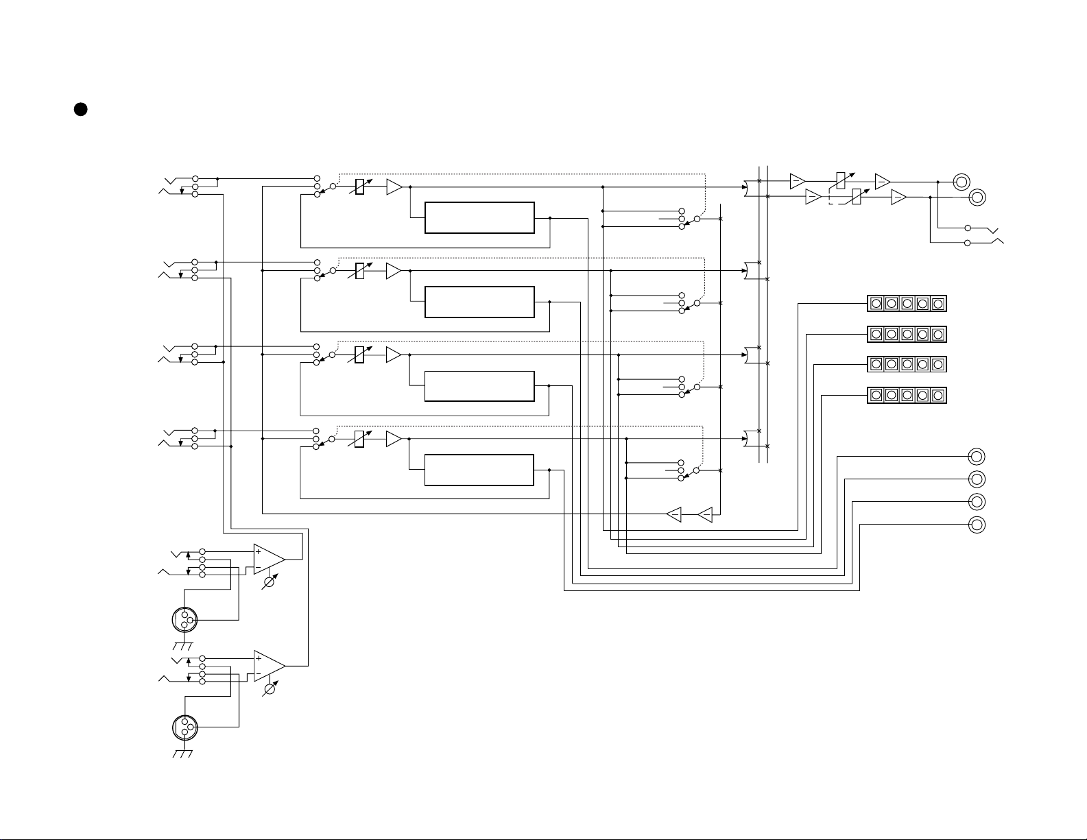
BLOCK DIAGRAM
LINE IN/INSERT
-10dBV
1
TIP: RTN
RING: SEND
REC
A. B REC
LINE OUT
PAN
PB
INPUT
FADER
REC TRK 1
REC
A. B REC
PB
MASTER
FADER
-10dBV
L
R
LINE IN/INSERT
-10dBV
LINE IN/INSERT
-10dBV
LINE IN/INSERT
-10dBV
MIC IN
-10dBV <--> -50dBV
1/3
2
TIP: RTN
RING: SEND
3
TIP: RTN
RING: SEND
4
TIP: RTN
RING: SEND
A. B REC
REC
A. B REC
REC
A. B REC
REC
PAN
PB
INPUT
FADER
REC TRK 2
REC
A. B REC
BARGRAPH
PB
PAN
PB
INPUT
FADER
REC TRK 3
REC
A. B REC
PB
PAN
PB
INPUT
FADER
REC TRK 4
REC
A. B REC
PB
PHONES OUT
16 ohm 20mW
1
2
3
4
TAPE OUT
-10dBV
1
2
3
4
2
3
1
TRIM
25
MIC IN 2/4
-10dBV <--> -50dBV
2
3
1
TRIM
X-24
Page 26

FOSTEX CORPORATION 3-2-35 Musashino, Akishima, Tokyo, Japan 196-0021
FOSTEX CORPORATION OF AMERICA 15431 Blackburn Ave., Norwalk, CA 90650, U.S.A.
© PRINTED IN JAPAN JUNE 1998 8288772000
 Loading...