

Programmable Automatic RCL Meter
PM6304
Service Manual
This Service Manual is also valid for PM6304C.
9 51 11 1

Now incorporating Philips T&M... FLUKE
IMPORTANT
in correspondence concerning the Programmable Automatic RCL Meter please give the model number and serial number as located on the type number plate on the instrument.
For your reference:
| Model number: | PM6304/xxx |
|---|---|
| Code number: | 9452 063 04xxx |
| Serial number: | LO XXXXXX |
Note: The design of this instrument is subject to continuous development and improvement. Consequently, this instrument may incorporate minor changes in detail from the information contained in this manual.
Warning These servicing intructions are for use by qualified personnel only. To reduce the risk of electric shock, do not perform any servicing other than that specified in the operating instructions unless you are fully qualified to do so.
4822 872 15169 0/11-November-1995 © 1995 Fluke Corporation, Inc. All rights reserved. Printed in Germany. All product names are trademarks of their respective companies.
CONTENTS
| 1 | SAF | ETY INS | STRUCTIONS | - | 1 - 1 |
| 1.1 | SAFET | Y PRECAUTIONS | 1 - 1 | ||
| 1.2 | CAUTI | ON AND WARNING STATEMENTS | 1 - 1 | ||
| 1.3 | SYMBO | OLS | 1 - 1 | ||
| 1.4 | IMPAIF | RED SAFETY PROTECTION | 1 - 2 | ||
| 1.5 | GENER | RAL CLAUSES | 1 – 2 | ||
| • | 1.1615 | ||||
| 2 | LINE | : VOLIA | AGE SETTING AND FUSES | а | 2 - 1 |
| 3 | PRIM | CIPLE | OF OPERATION AND MEASUREMENT | 3 – 1 | |
| ×. | 3.1 | INTRO | DUCTION | 3 — 1 | |
| 3.2 | DESCF | RIPTION OF THE BLOCK DIAGRAM, Figure 10, 11 | 3 - 2 | ||
| 3.3 | PRINC | IPLE OF MEASUREMENT | 3 - 4 | ||
| 4 | CIRC | SCRIPTION, TROUBLESHOOTING | 4 - 1 | ||
| 4.1 | POWE | R SUPPLY, UNIT 1, Figure 16 | 4 - 1 | ||
| 4.2 | CENTR | AL PROCESSING UNIT, CPU, UNIT 2, Figure 18 | 4 - 1 | ||
| 4.3 | SIGNA | L SYNTHESIZER, UNIT 2, Figure 19 | 4 - 3 | ||
| 4.4 | COUN | TER, UNIT 2, Figure 20 | 4 - 4 | ||
| 4.5 | ANALO | G UNIT, Figures 22 to 28 | 4 - 5 | ||
| SOURC | CE, UNIT 3, Figure 22 | ||||
| 4.6 | SELEC | TOR, Figure 23 | 4 - 8 | ||
| 4.7 | AC/V C | ONVERTER, Figure 24 | 4 - 9 | ||
| 4.8 | AMPLIF | FIER, Figure 25 | 4 - 10 | ||
| 4.9 | FILTER | Figure 26 | 4 - 10 | ||
| 4.10 | MULTIF | PLYING DAC, Figure 27 | 4 - 11 | ||
| 4.11 | DUAL-S | SLOPE INTEGRATOR, Figure 28 | 4 - 12 | ||
| 4.12 | KEYBO | ARD / DISPLAY, UNIT 4, Figure 30 | 4 - 14 | ||
| 4.13 | DC UN | IT 5. Figures 32, 33 | 2 | 4 - 19 | |
| DC/V C | CONVERTER. Figure 32 | ||||
| 4.14 | DC/AC | CONVERTER, Figure 33 | 4 - 20 | ||
| 4.15 | HANDL | ER INTERFACE, UNIT 6, Figure 35 | 4 - 20 | ||
| 4.16 | IEEE-4 | 88 INTERFACE, Figure 39 | 4 - 22 | ||
| RS-232 | NTERFACE, Figure 37 | 4 - 22 | |||
| 5 | PER | FORMA | NCE TEST | 5 – 1 | |
| 5.1 | INTRO | DUCTION | 5 - 1 | ||
| 5.2 | RECON | MMENDED TEST EQUIPMENT | 5-1 | ||
| 5.3 | SELF-T | EST ROUTINE | 5-2 | ||
| 5.4 | PERFC | RMANCE VERIFICATION | 5 - 2 | ||
| T .0.0 | 5.4.1 | Test Signal Voltage | 5-2 | ||
| 5.4.2 | Test Signal Frequency | 5 - 3 | |||
| 5.4.3 | Open-Circuit Trimming | 5-3 | |||
| 5.4.4 | Short-Circuit Trimming | 5 - 3 | |||
| 5.4.5 | AC Measurements | 5-3 | |||
| 5.4.6 | DC Measurements | 5-6 | |||
| 2014 | A ANTINE A TIME OF THE CONTRACT AND A MARKET |
Page
| 0-2 | CONTENTS | PM630 |
|---|---|---|
| 6 | RECALIBRATION | 6 - 1 |
| 6.1 GENERAL | 6 - 1 | |
| 6.2 RECALIBRATION WITH THE PM 9559 BIN PROGRAMMER | 6 - 2 | |
| 6.3 RECALIBRATION VIA IEEE-488 OR RS-232 INTERFACE | 6 - 4 | |
| 7 | DISASSEMBLING THE INSTRUMENT | 7 – 1 |
| 7.1 GENERAL INFORMATION | 7 - 1 | |
| 7.2 REMOVING THE COVERS | 7 - 1 | |
| 7.3 UNIT 8 (RS-232 INTERFACE) OR UNIT 9 (IEEE-488 INTERFACE) | 7 - 2 | |
| 7.4 UNIT 6. HANDLER INTERFACE | 7 - 2 | |
| 7.5 UNIT 2. DIGITAL UNIT | 7 - 3 | |
| 7.6 UNIT 1. POWER SUPPLY | 7 - 3 | |
| 7.7 UNIT 3. ANALOG UNIT | 7 - 4 | |
| 7.8 UNIT 4. KEYBOARD/DISPLAY | 7 - 4 | |
| 7.9 UNIT 7. FLEXPRINT | 7 - 5 | |
| 7.10 UNIT 10. CONNECTOR UNIT, AND ROUND CONNECTOR | 7 - 5 | |
| 7.11 UNIT 5. DC UNIT | 7 - 5 | |
| 7.12 ROD AND HOLDER FOR POWER SWITCH | 7 - 6 | |
| 7.13 POWER SWITCH | 7 - 6 | |
| 7.14 TEXT PLATE | 7 - 6 | |
| 8 | SELE DIAGNOSTIC AND TROUBLESHOOTING | 8 - 1 |
| • | 8 - 1 | |
| PROGRAM 2: KEYBOARD TEST | 8 - 1 | |
| PROGRAM 3: BIN PROGRAMMER TEST | 8-2 | |
| PROGRAM 4' MEMORY REGISTER TEST | 8 - 2 | |
| PROGRAM 5' EEPROM TEST | 8 - 2 | |
| PROGRAM 6: STROBE TEST (TEST OF THE INTERNAL INTERFACE) | 8 - 3 | |
| PROGRAM 7: MEASUBEMENT DATA TEST | 8 - 3 | |
| PROGRAM 8: CALIBRATION DATA TEST | 8 - 11 | |
| PROGRAM 9: INTERFACE TEST (RS-232 OR IEEE-488) | 8 - 13 | |
| 9 | 9 - 1 | |
| 10 | INSTALLATION INSTRUCTIONS FOR OPTIONS | 10 - 1 |
| 10.1 DM 0548 IEEE_AR8 INTEREACE | 10 - 1 | |
| 10.2 PM 0549 RS-232 INTERFACE | 10 - 1 | |
| 10.3 PM 9565 DC UNIT | 10 - 5 | |
| 10.4 PM 9566 HANDLEB INTERFACE | 10 - 5 | |
| 10.5 PM 9564 19" RACK MOUNT ADAPTER | 10 - 9 | |
| 11 | CHECKING AND ADJUSTING | 11 _ 1 |
| 44 | ||
| 11 - 1 | ||
| 11 - 1 | ||
| 11.3.1 Internal Sunniv Voltages | 11-2 | |
| 11.3.2 Clock Frequency | 11 - 2 | |
| 11 - 2 |
| 11.3.4 DC Offset Voltage | 11 - 3 | ||
| 11.3.5 DC Supply Voltages | 11 - 4 | ||
| 11.3.6 Functional Check | 11 – 4 | ||
| 11.3.7 Recalibration | 11 - 5 | ||
| 11.3.8 Measurement Accuracy | 11 – 5 | ||
| 11.3.9 Dissipation Factor | 11 – 5 | ||
| 11.3.10 Short-Time Deviation of Measurements | 11 - 5 | ||
| 11.3.11 Fast Mode via IEEE-488 or RS-232 Interface | 11 - 6 | ||
| 11.3.12 PM 9566 Handler Interface, PM 9559 Bin Programmer | 11 - 6 | ||
| 12 | SAF | ETY INSPECTION AND TESTS AFTER REPAIR AND | 12 – 1 |
| MAI | NTENANCE IN THE PRIMARY CIRCUIT | ||
| 12.1 | GENERAL DIRECTIVES | 12 - 1 | |
| 122 | SAFETY COMPONENTS | 12 - 1 | |
| 12.2 | CHECKING THE PROTECTIVE GROUND CONNECTION | 12 - 1 | |
| 12.0 | 12 - 1 | ||
| 12.4 | CRECKING THE INSUEATING RESISTANCE | 12 - 1 | |
| 13 | SPAR | RE PARTS, Figures 13.1, 13.2 | 13 - 1 |
| 13.1 | GENERAL | 13 – 1 | |
| 13.2 | STANDARD PARTS | 13 – 1 | |
| 13.3 | SPECIAL PARTS | 13 - 1 | |
| 13.4 | TRANSISTORS AND INTEGRATED CIRCUITS | 13 – 1 | |
| 13.5 | STATIC-SENSITIVE COMPONENTS | 13 – 2 | |
| 13.6 | HANDLING MOS DEVICES | 13 – 2 | |
| 13.6.1 Storage and Transport | 13 – 2 | ||
| 13.6.2 Testing or Handling | 13 – 2 | ||
| 13.6.3 Mounting | 13 - 2 | ||
| 13.6.4 Soldering | 13 - 2 | ||
| 13.6.5 Static Charges | 13 – 3 | ||
| 13.6.6 Transient Voltages | 13 - 3 | ||
| 13.7 | SOLDERING TECHNIQUES | 13 - 3 | |
| 3.7.1 Surface Mounted Devices (SMD) Handling and Replacement | 13 – 4 | ||
| 13.8 | MAINS CABLES | 13 - 7 | |
| 13.9 | MECHANICAL PARTS, HOUSING (Figure 13.1) | 13 - 9 | |
| 13.10 | MECHANICAL PARTS ON UNITS, CABLES, | ||
| PARTS NOT ON UNITS, MISCELLANEOUS (Figure 13.2) | 13 - 11 | ||
| 13.11 | ACCESSORIES, ADAPTERS (Figures 1 to 9) | 13 - 12 | |
| 13.12 | ELECTRICAL PARTS ON UNITS | 13 - 13 | |
| Unit 1, Power Supply, Figures 13, 16 | 13 - 13 | ||
| Unit 2. Digital Unit, Figures 17 to 20 | 13 - 14 | ||
| Unit 3. Analog Unit, Figures 21 to 28 | 13 - 16 | ||
| Unit 4. Keyboard/Display, Figures 29, 30 | 13 - 24 | ||
| Unit 5. DC Unit. Figures 31, 32, 33 | 13 - 25 | ||
| Unit 6, Handler Interface, Figures 34, 35 | 13 - 26 | ||
| Unit 7, Flexprint, Figure 14 | 13 - 27 | ||
| Unit 8, RS-232 Interface, Figures 36, 37 | 13 - 27 | ||
| Unit 9, IEEE-488 Interface, Figures 38, 39 | 13 - 29 | ||
| Unit 10, Connector Unit, Figure 15 | 13 - 29 |
Fig. 1 Front View Fig. 2 Rear View Fig. 3 PM 9540/TWE, SMD Tweezers Fia. 4 PM 9540/BAN 4-wire Test Cable with Banana Plugs Fig. 5 PM 9541A, 4-wire Test Cable Fig. 6 Single and Double Test Posts Fia. 7 PM 9542SMD, SMD Adapter Fig. 8 PM 9542A, BCL Adapter Fig. 9 PM 9559 Bin Programmer, Infrared Remote Control Fia. 10 Basic Block Diagram Fig 11 Detailed Block Diagram Fig. 12 Overall Circuit Diagram Unit 1, Power Supply: Component Layout Fig 13 Fig. 14 Unit 7, Flex Print Fig. 15 Unit 10 Connector Unit Fig. 16 Unit 1. Power Supply Fig. 17 Unit 2, Digital Unit; Component Layout Fig. 18 Unit 2, Central Processing Unit, CPU Fig. 19 Unit 2. Signal Synthesizer Fig. 20 Unit 2, Counter Fig. 21.1 Unit 3, Analog Unit; Component Layout, Part 1 Fig. 21.2 Unit 3, Analog Unit; Component Layout, Part 2 Fig. 22 Unit 3. Source Fig. 23 Unit 3. Selector Fig. 24 Unit 3, AC/V Converter Fig. 25 Unit 3. Amplifier Fig. 26 Unit 3. Filter Fig. 27 Unit 3, Multiplying DAC Fig. 28 Unit 3, Dual Slope Integrator Fig. 29 Unit 4, Keyboard/Display; Component Layout Fig. 30 Unit 4, Keyboard/Display Fig. 31 Unit 5. DC Unit; Component Layout Fig. 32 Unit 5. DC/V Converter Fig. 33 Unit 5, DC/AC Converter Fig. 34 Unit 6, Handler Interface; Component Layout Fig. 35 Unit 6. Handler Interface Fig. 36 Unit 8, RS-232 Interface; Component Layout Unit 8, RS-232 Interface Fig. 37 Fig. 38 Unit 9, IEEE-488 Interface; Component Layout
Fig. 39 Unit 9, IEEE-488 Interface
SERVICE CENTRES
0 - 4
FIGURES
1 SAFETY INSTRUCTIONS
WARNING
These service instructions are for use by qualified personnel only. To reduce the risk of electric shock, do not perform any servicing other than that specified in the Operating Instructions unless you are fully qualified to do so.
Read these pages carefully before installation and use of the instrument.
The following clauses contain information, cautions, and warnings which must be followed to ensure safe operation and to keep the instrument in a safe condition. Adjustment, maintenance, and repair to the instrument shall be carried out only by gualified personnel.
1.1 SAFETY PRECAUTIONS
For the correct and safe use of this instrument it is essential that both operating and servicing personnel follow generally accepted safety procedures in addition to the safety precautions specified in this manual. Specific warning and caution statements, where they apply, will be found throughout the manual. Where necessary, the warning and caution statements and/or symbols are marked on the apparatus.
1.2 CAUTION AND WARNING STATEMENTS
CAUTION
Is used to indicate correct operating or maintenance procedures to prevent damage to or destruction of the equipment or other property.
WARNING
Calls attention to a potential danger that requires correct procedures or practices to prevent personal injury.
1.3 SYMBOLS
Protective earth (black symbol on yellow background) (grounding) terminal
1.4 IMPAIRED SAFETY PROTECTION
Whenever it is likely that safety protection has been impaired, the instrument must be disconnected from power and be secured against any unintended operation. The matter should then be referred to qualified technicians. Safety protection is likely to be impaired if, for example, the instrument fails to perform the intended measurements or shows visible damage.
1.5 GENERAL CLAUSES
WARNING
The opening of covers or removal of parts, except those to which access can be gained by hand, is likely to expose live parts and accessible terminals which can be dangerous.
The instrument shall be disconnected from all voltage sources before it is opened.
Capacitors inside the instrument can hold their charge even if the instrument has been removed from all voltage sources.
WARNING
Any interruption of the protective earth conductor inside or outside the instrument, or disconnection of the protective earth terminal, is likely to make the instrument dangerous. Intentional interruption is prohibited.
Components which are important for the safety of the instrument may only be replaced by components obtained through your local Fluke organization (see also Chapter 13).
After repair and maintenance in the primary circuit, safety inspection and tests, as mentioned in Chapter 12, must be performed.
2 LINE VOLTAGE SETTING AND FUSES
The safety instructions in the previous chapter must be followed.
Before plugging in the power cord make sure that the instrument is set to the local line voltage.
WARNING
If the power cord has to be adapted to the local situation, such adaption should be done by a qualified person only.
On delivery from the factory the instrument is set to one of the following line voltages:
| Туре | Code no. | Line voltage |
Delivered
power cord |
|---|---|---|---|
| PM6304 | 9452 x63 04xx1 | 220 V | Universal Europe |
| PM6304 | 9452 x63 04xx3 | 120 V | North America |
| PM6304 | 9452 x63 04xx4 | 240 V | England (U.K.) |
| PM6304 | 9452 x63 04xx5 | 220 V | Switzerland |
| PM6304 | 9452 x63 04xx8 | 240 V | Australia |
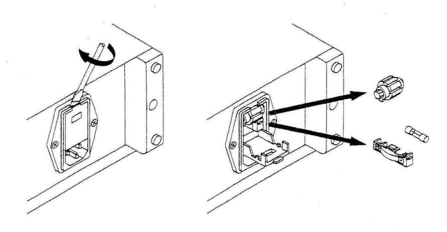
The set line voltage and the corresponding fuse rating are indicated on the rear panel.
Make sure that replacement fuses are of the type and current rating specified. You also may use fuses according to UL/CSA instead of the built-in type according to IEC 127. The use of repaired fuses and/or short circuiting of fuse holders are prohibited. Do not defeat this important safety feature.
The instrument can be set to the following line voltages: 100 V, 120 V, 220 V and 240 V ac. These nominal voltages can be selected via the voltage selector, located at the rear panel, adjacent to the power socket. The fuse is located in a holder at the same place. For line power voltage selection or replacement of the fuse, remove the power cord and pry open the compartment with a small screwdriver (see drawing next page).
Select one of the voltage ranges, as appropriate, by turning the selector. If necessary, insert the specified fuse (T0.2A or T0.4A according to IEC127 or T0.25A or T0.5A according to CSA/UL198G) that matches the line voltage setting into the fuse holder.
3 PRINCIPLE OF OPERATION AND MEASUREMENT
3.1 INTRODUCTION
The two-pole CUT (Component Under Test) Zx is connected to the SELECTOR section of the instrument by four wires:
- Via the HD (High Drive) wire. The sinusoidal ac or the dc test voltage from the SOURCE or the DC source is routed to one CUT terminal by means of this wire.
- Via the LD (Low Drive) wire, which is forced electronically to near ground voltage level. The current through the CUT is routed by means of this wire either to the AC/V CONVERTER or, in the dc measuring mode, to the DC/V CONVERTER.
- By the HS (High Sense) and LS (Low Sense) wires, the voltages at the CUT terminals are picked for processing.
In the dc-measuring mode, the sense voltages from the CUT and the DC/CONVERTER output voltages are converted to a 2 kHz ac voltage by the DC/AC CONVERTER in the DC UNIT. Within one measuring cycle, these voltages or, for the ac-measuring mode, the sense voltages from the CUT and the AC/V CONVERTER output voltage, are processed alternately in the AMPLIFIER-FILTER-MUL-TIPLYING DAC channel. In the DAC, the individual sinusoidal measuring voltage at A5 is multiplied successively by two quadrature-phase reference sine waves from the SIGNAL SYNTHESIZER, thus creating at A6 dc voltages proportional to the in-phase components of the measuring voltage. These dc terms are converted to binary numbers by a dual-slope ADC, consisting of the DUAL-SLOPE INTEGRATOR and the COUNTER, which are then read by the CPU. At the end of one measuring cycle in the ac measuring mode, seven numbers are normally in the CPU RAM:
- Two "voltage numbers" for the two quadrature-phase components of the CUT voltage.
- Two "current numbers" for the two guadrature-phase components of the CUT current.
- One "voltage reference" number for the main ac component of the CUT voltage measuring channel, short-circuited at the ac selector input.
- A "current reference" number for the main ac component of the CUT current measuring channel, short-circuited at the ac selector input.
- A quadrature-phase "voltage reference" or "current reference" number, depending on the used larger amplifier gain.
These seven numbers, the appropriate amplifier gains and reference sine wave phases, the instrument trim and calibration data, all combine to form the basis for the calculation of the CUT parameters. The calculation is performed by the CPU according to pre-defined algorithms. The results is transferred to the display.
3.2 DESCRIPTION OF THE BLOCK DIAGRAM, Figures 10, 11
SIGNAL SYNTHESIZER
The TWS (Triangle Wave Synthesizer) reads out sine wave tables loaded in the sine wave PROMs. and so creates 8-bit-word sequences of the test signal, the reference sine wave for the MULTIPLYING DAC and the DC/AC CONVERTER in the DC UNIT. The test signal is converted to an analog sine wave by the DAC. The CPU controls frequency and phase settings.
SOURCE
The test signal is filtered within the SOURCE section and set to the programmed high, normal or low level amplitude by the ac source. A bias regulator generates the dc current for fast biasing of tested capacitors. Overload protection circuits protect the test signal source and the bias source from being damaged by external load.
SELECTOR
The source resistor belonging to the selected test signal level is switched on by relays. The ac selector multiplexes the CUT voltage behind the sense buffer stages, the voltage from the AC/V CONVERTER and, for the reference measurements, the ground level. A differential amplifier pre-amplifies and buffers the multiplexed voltages in ac measuring mode. The AC/V CONVERTER converts the CUT current to a proportional ac voltage. The dc selector multiplexes the CUT terminal voltages and the voltage from the DC/V CONVERTER to the DC/AC CONVERTER in the DC UNIT. A bias selector inhibits the bias currents or routes either the EXTERNAL BIAS or the internal bias current from the SOURCE to the CUT.
DC UNIT
The DC voltage source, the DC/V CONVERTER for the CUT current and the DC/AC CONVERTER form the DC UNIT.
The DC/AC CONVERTER converts the measuring voltages from the CUT terminals and the DC/V CONVERTER output voltage to a 2 kHz sine wave voltage. This is achieved by multiplication with the 2 kHz digital wave from the SIGNAL SYNTHESIZER.
AMPLIFIER
The preamplifier equalizes the amplitude differences, depending on the test signal level. The main amplifier-voltage divider channel is controlled by the CPU and set to such an overall gain, that at the output of the FILTER section, the window detector senses the in-range condition. For very low CUT voltages or currents, i.e., very low or very high CUT impedances, the corresponding gains are set to maximum.
FILTER
Depending on the selected test frequency, the AMPLIFIER output signal is filtered by a 300 Hz LPF, a 300 Hz to 20 kHz BPF, or a 100 kHz BPF. The output is buffered and sensed by the window detector (see Section AMPLIFIER).
MULTIPLYING DAC
The FILTER output signal is multiplied by the digital reference sine wave from the SIGNAL SYNTHE-SIZER. For the CUT voltage signal and the CUT current signal, two quadrature-phase reference signals are successively used (see introduction). The polarity detector provides the CPU with information about the right phase settings.
DUAL-SLOPE INTEGRATOR
The DUAL-SLOPE INTEGRATOR executes for each analog/digital conversion first, for a fixed period, the dc integration and then the de-integration to zero with a fixed dc input. This is always monitored by the timer within the COUNTER section and of the CPU. The reset & hold circuit sets the initial zero output voltage condition of the integrator.
COUNTER
During the de-integration period of the DUAL-SLOPE INTEGRATOR the COUNTER accumulates the number of the count-clock pulses. The final number, which is proportional to the integrated dc input, is read out by the CPU (see introduction). The timer controls the integration period of the DUAL-SLOPE INTEGRATOR. DUAL-SLOPE INTEGRATOR and COUNTER represent the dual-slope ADC.
CPU, LCD & KEYBOARD, IR DETECTOR
The instrument is operated from the KEYBOARD, or remotely by the IEEE-488 or the RS-232 Interface, or via the IR DETECTOR from the Bin Programmer. The CPU processes these instructions as well as the information from the window and the polarity detector for controlling the various functional units in the instrument. The computation results, derived from the measurement data, are transferred to the LCD, the HANDLER Interface and the IEEE-488 or the RS-232 Interface.
POWER SUPPLY
The POWER SUPPLY provides dc supply voltages for the various functional units in the instrument, a dc current for the LCD backlight, and ac supply voltages for the IEEE-488 or the RS-232 Interface, and the HANDLER Interface. The data lines for the Handler Interface are routed through the Power Supply.
3.3 PRINCIPLE OF MEASUREMENT
The component measurement is based on the current and voltage technique. The component voltage and the component current are measured and converted into binary values. From these values the CPU calculates the electrical parameters of the component. According to the front panel parameter selection, either the dominant and secondary parameters are automatically displayed (AUTO) – resistance, capacitance or inductance, or the manual selected parameter (Q, D, Z, or Φ) is displayed.
Each measurement cycle lasts approximately 0.5 seconds and consists of seven single measurements, the results of which are stored and arithmetically evaluated. Finally the result is transferred to the display. The seven single measurements are as follows:
1. Voltage Measurement: 0°
- and internal gain factor setting
- 2. Voltage Measurement: 90°
- 3. Reference Measurement: 0°
| Gain factor >1 | Gain factor = 1 | |||
|---|---|---|---|---|
| 4. | Reference Measurement: | 90° | Current Measurement: | 00 |
| 5. | Current Measurement: | 00 | Current Measurement: | 90° |
| 6. | Current Measurement: | 90° | Reference Measurement: | 00 |
| 7. | Reference Measurement: | .00 | Reference Measurement: | 90° |
The seven measured values are stored at the end of the single measurements. The processor uses the measured values to calculate the equivalent series resistance Rs, the equivalent series reactance Xs, and the quality factor Q = Xs/Rs of the component. In AUTO mode the processor determines the dominant and secondary parameter, calculates its value, and displays it together with the equivalent circuit symbol. If one of the other parameters is manually selected, this parameter is calculated and displayed. After that the next measurement cycle starts with the seven single measurements.
The display shows:

The following phase diagrams and formulas show the mathematic basics for internal calculation of the component value.
voltage

l: current V1, V2: 0°-voltage, 90°-voltage The phase angle between I and V is o.
The phase angle between I and V1 is a .
In the diagram the phase relation between I and V is related to a lossy inductance. In each measurement cycle, the following components are determined: Vp, Vq, Ip, Iq. The series resistance and reactance are calculated from these components.
| Vpip + Vqi | q (1) | Ve | Vqlp - Vplq | |
|---|---|---|---|---|
|
HS =
Ip 2 + Iq 2 |
AS = | lp 2 + lq 2 | (2) |
The following equivalent circuit is valid:
φ Rs R
Quality factor: Q = tan φ = 1/D = (3) Dissipation factor: D = tan δ = 1/Q = (4)
The magnitude of Q and the sign of Xs determine which parameter of the component is dominant.
Xs positive = inductive Xs negative = capacitive
The formulas for the various parameters are as follows:
| Q = |Xs| / Rs see equation (3) | Z = \sqrt{Rs}^2 + Xs^2 |
|---|---|
| D = 1/Q | Cp = \frac{1}{\omega(1 + 1/Q^2)|Xs|} if Xs < 0 |
| Rp = (1 + Q 2 ) x Rs | Lp = \frac{(1 + 1/Q^2)|Xs|}{\omega} \text{if Xs > 0} |
| Rs see equation (1) | Cs = 1/(m |Xs|) if Xs < 0 |
| Ls = if Xs > 0 | |
| Impedance Z = R + iX |
Admittance Y = 1/Z
____

The decision criterion for selecting the dominant parameter is Q = D = 1. The values Q and D not only depend on the component but also on the test signal frequency used.
AUTO MODE DECISION DIAGRAM
Example:
By using the seven measurements, the instrument has calculated Bs and Xs in accordance with formulas 1 and 2, for example:
From this the instrument calculated:
The instrument displays the corresponding equivalent circuit symbol with the dominant and the secondary component, according to the criteria of the Auto Mode Decision Diagram; in this case, as Xs is pegative and 1 < 0 < 1000:
The display shows:

The calculation of the dominant parameter Cp was done according to the following formula: Cp = -
The maximum display is five digits ±1 digit tolerance.
Calculation of the other selectable parameters are performed as follows: D =
Rs = 3.068 kΩ (calculated by the instrument according to formula 1)
: The instrument calculates
and gets from an internal tangent table similar to a calculator Φ = - 78.6 DEG
For accurate measurement, you should select an appropriate test signal frequency, see Section 4.2 of the Users Manual.
If you measure the same component mentioned in the example before, with a test signal frequency that is too low, the resistive part of the capacitive parameter dominates. So the instrument determines a resistor as the dominant parameter.
Example: Test signal frequency 100 Hz

The instrument determined: Rs = 63.248 kΩ Xs = -31.680 kΩ
and calculated:
Because Q<1, the display shows a resistor as the dominant parameter.
Calculation of the other parameter is performed by the same formulas: D = 1/C = 2.00
Q
Rp = (1 + Q2) x Rs = 79.123 kΩ
Rs = 63.248 kΩ (calculated according to formula 1)
Φ = - 26.6 DEG


----
PM6304


4 CIRCUIT DESCRIPTION, TROUBLESHOOTING
4.1 POWER SUPPLY, UNIT 1, Figure 16
The Power Supply on Unit 1 generates five stabilized dc voltages: +15 V, -15 V, +5 VA, -5 V for the analog circuitries, and +5 V for the digital circuitries.
You can check all voltages at the test socket X104.
Potentiometer R115 adjusts the +15 V supply. The stability depends on the reference diode V159. The -15 V supply is derived from +15 V via resistors R118, R119; so there is no further adjustment.
When you switch power off or when the +5 V supply fails, the power down signal PD at transistor V101 and Z-diode V152 gets low before the +5 V supply is below 3.5 V output voltage. PD low and so RST high reset the processor D107 on the CPU, Unit 2, Figure 18, thus preventing any further data exchange until the internal supply voltages are completely down. Furthermore, SRAM D103 on the CPU, where the instrument settings are stored, is now backed up by the battery G150.
The same happens when you press the concealed front panel RESET switch, Figures 29, 30 (only for instruments until LO 648 884). When you switch power on, low signal at capacitor C102 in Figure 18 resets the processor.
Resistor R127 and Z-diode V160 together with the secondary ac voltage of the transformer generate the rectangular SFR signal. On the CPU, the instrument measures the signal period and so identifies whether there is 50 Hz or 60 Hz mains frequency.
Amplifier N106 and transistor V106 generate the current for the backlight of the display. Via the BLS line the brightness is adjusted by potentiometer R101 on Unit 4, Figure 30.
The ac voltages for the interfaces are fed via the power supply, connection X103.1-4. Multi-fuse F111 protects Unit 6. Handler Interface.
For Units 8/9, IEEE-488/RS-232 Interface, there is no fuse necessary. Short cuts on these units will blow up the mains fuse.
4.2 CENTRAL PROCESSING UNIT, CPU, UNIT 2, Figure 18
The CPU contains the 8-bit processor (microcontroller) D107, program memory (EPROM) D105, address latch D106, input port extension D108, battery buffered RAM D103 for storage of instrument settings including TRIM data, and the EEPROM D104 for storage of calibration and binning data. The processor is clocked by the 12 MHz Clock Oscillator, crystal G101. This clock is also used for the counter, Figure 20.
The multiplexed address/data bus P0 of the processor supplies the address inputs A0 to A7 of the EPROM via the address latch, switched by ALE (Address Latch Enable). The address inputs A8 to A15 of the EPROM are directly supplied from the processor port P2. Data are transferred from the EPROM outputs ACT0 to ACT7 to the processor port P0 via the multiplex bus, controlled by PSEN (Program Store Enable). Via this bus also the data from the input port D108 are read in, selected by the RD signal.
The communication between processor and the four interfaces is performed via the bidirectional I2C-bus with data line SDA and clock line SCL:
- RAM for the instrument settings.
- IEEE-488 respectively RS-232 Interface.
- Display drivers on Unit 4, and
- EEPROM, for which a separate address line SDA2 is provided.
The principle of data transfer via I2C-bus is shown in the following diagram.

The C-bus , lines SD, SC, and strobe lines STR1 to 4 and 6, transfers the data to the different units. The serial data SD are clocked into shift registers by the clock SC; the following assigned strobe latches the data in the selected shift register and presents the serial transmitted information in parallel form at the output of the register.
The strobe decoder D109 generates the strobes STR1 to 4 and 6, controlled by the processor, AD8 to 10 and WR.

Fig. 4.1 Principle of Latch and Shift Register
For troubleshooting see also Chapter 8, Self Diagnostic and Troubleshooting, Program 6, Strobe Test.
The strobes control the following circuits:
STR1: Signal Synthesizer, shift register D202 (TWS), Figure 19
STR2: Signal Synthesizer, shift register D206, Figure 19
STR3: Selector, shift register D201, Figure 23
STR4: Source, shift register D101. Figure 22
Amplifier, shift register D401, Figure 25
STR6: Handler Interface, D106/D107, Figure 35
When you switch power off or when the +5 V supply fails, SRAM D103, where the instrument settings including the TRIM data are stored, is supplied with a 3 V battery to avoid loss of stored data. Additional pin 7 (TEST) is provided with this voltage; by this the SRAM is set in a mode that reduces power consumption. For the power down signal PD, see Section 4.1, Power Supply.
4.3 SIGNAL SYNTHESIZER, UNIT 2, Figure 19
The Signal Synthesizer generates the test frequencies 50 Hz to 100 kHz . The outputs are the analog sine wave F_MEAS at connector X155 for the Source on Unit 3, and the digital sine wave at X108 for the Multiplying DAC on Unit 3, and for the DC/AC Converter on the DC Unit 5.
The Triangle Wave Synthesizer , TWS D202, is clocked by the 20.97 MHz Oscillator, crystal G201, adjusted by C210. The TWS generates a sequence of read addresses for the Sine PROMs D204, D207. The PROMs are loaded with binary values for the sample magnitudes of the sine wave, which are read out according to the addresses sent by the TWS. The binary values are converted into an analog sine wave by the Digital to Analog Converter , DAC N201, with 8 bit amplitude resolution. A Lowpass/Bandpass Filter in the Source on Unit 3 smooths the sine wave and suppresses clock and alias frequencies of the digital frequency synthesis.

Fig. 4.2 Signal Syntheziser, Simplified Diagram
_
The TWS D202 contains a shift register which converts the serial control data fed in via the C-bus to parallel data. A part of this serves as a phase increment for an internal phase accumulator. This increment is accumulated with each clock pulse. The output, latched by D203, is a 10 bit word which represents the current read address for the subsequent Sine PROM D204, increasing with each clock pulse (0 to 1023).
The clock CK02 for the latches derived from the clock input FCI is 20.97 MHz for test frequencies >2 kHz; for test frequencies ≤2 kHz. CK02 is reduced by 10 to 2.097 MHz.
The DAC N201 has a separate 5 V supply, voltage regulator N202.
For DC measurements the AC signal is switched off, output AC OFF, shift register D206.
For the digital sine wave the phase is switched from 0° to 270° in steps of 90°, adding the outputs PHI_B0_PHI_B1 of shift register D206 to the two MSBs of latch output D203.
The clock for the digital sine wave is divided by 8, counter D209. The Multiplying DAC on Unit 3 requires this reduced clock.
4.4 COUNTER, UNIT 2, Figure 20
The circuit diagram comprises three parts:
The Timer is clocked by the 12 MHz Clock Oscillator on the CPU. The timer defines the integration periods 5 ms, 40 ms, or 50 ms of the Dual-Slope Integrator by the Divider by 3 (D301), the selectable Divider by 2 or by 16 (D312), or by 20 (D302), and the Divider by 10000 (2 times by 100, D304, D305). The 20 Bit Counter counts the 20.97 MHz pulses during the de-integration period of the Dual-Slope Integrator, which together represent a dual-slope analog to digital converter (ADC). The final counter state, which is proportional to the integrator dc input, is read out by the CPU. The Control Logic , flipflops D307, D314, controls the Timer and the Counter.
Figure 4.3 shows the timing diagram for one conversion period of the ADC:

Fig. 4.3 Timing Diagram for One Conversion Period at the ADC
Low pulse START at D306.13 prepares the conversion at t1. D307.9 is set to high, the reset input D307.15 is released. For synchronization with the test voltage, the next trailing edge of the MSB_FMEAS signal starts the integration, HOLD signal D306.1 and INTGR D307.6 get low. D307.5 releases the reset for the divider and sets the 20 bit counter to 0. The carry of the timer, trailing edge D305.13 at t3, sets the output D307.9 to low, and so D307.15 resets the INTGR signal to high. At the same time, the COUNT output D314.6 gets low and starts the de-integration: NOR gate D306.4 switches the 20.97 MHz count pulses to the 20 bit counter.
Zero output voltage of the integrator N703.1 on Unit 3 switches the EOD signal D314.13, End Of De-integration, from high to low, t4. Output D314.7 gets low and via D314.15 resets the COUNT signal to high. The counter stops, and the HOLD signal D306.1, NOR gate output of the INTGR and COUNT inputs, holds the integrator output at 0 V. The counter state at t4 is proportional to the integrator output voltage at t3 and, consequently, to the input value for this conversion.
The HOLD signal, inverted to READY via D211, Figure 19, is read by the CPU and terminates the conversion. The P_LOAD low pulse from the CPU, strobe decoder D109.7, loads the counter state into the shift registers D309, D311, D313. SC clocks the counter state via the serial data output SDO to the CPU.
If the integrator output passes -0.45 V at comparator N704 on Unit 3, for example, when changing the component during measurement, the I_RES signal gets low and interrupts the conversion via D307.14 and D314.10; HOLD signal discharges the integration capacitor to 0 V.
4.5 ANALOG UNIT, Figures 22 to 28 SOURCE, UNIT 3, Figure 22
General:
The Analog Unit comprises seven sections, Figures 22 to 28: Source, Selector, AC/V Converter, Amplifier, Filter, Multiplying DAC, Dual-slope Integrator.
For troubleshooting see also Chapter 8, Self Diagnostic and Troubleshooting, Program 7, Measurement Data Test, which statically checks the measurement channel from the component connector to the processor.
Figure 4.8, page 4 – 13, shows you the Principle Overall Diagram of the Analog Measurement Section, for AC mode.
The test signal from the Signal Synthesizer passes the Filter in the Source, and is set to the HIGH, NORMAL, or LOW level amplitude in the AC Source . A Bias Regulator generates the DC current for testing capacitors. Overload Protection circuits protect the test signal source from damages by external load. Figure 4.4 shows you the functional diagram including parts of the Selector, Figure 23.
N102 amplifies the 0.8 Vpp input to 2 V HIGH Level, adjusted by potentiometer R111. Divider chain R128 to R132 defines the 1 V NORMAL and 50 mV LOW Level. For 100 kHz test frequency, the 100 kHz Bandpass Filter BPF is selected. For all other frequencies, the 20 kHz Lowpass Filter LPF is selected. Buffer N105 with input lowpass filter R192/C121 and transistors V106, V107 generate the maximum 10 mA output current. Furthermore, a -0.7 V DC offset is superimposed on the AC signal for biasing the capacitor C222, Selector.
Relais K204, Selector, selects AC or DC measurement.
Diode switches V129 to V132 serve for Source Overload Protection. During normal operation, the positive and the negative current source are active, and the source signal is fed through. When the High Drive HD connection senses voltages above +45 V, transistor V117 switches off the positive current source and separates the diode switches from the source. The negative current source unloads the capacitor at the component connector.
For negative High Drive HD voltages below -45 V, the two current sources operate vice versa. For high VCF voltage, two transistors are cascaded, for example, V124, V125.
Capacitor C222 is switched in for AC measurement, relay K202; it is short cut for DC measurement. The internal or external DC bias voltage is fed in behind this capacitor.
The DC Bias Source with the Bias Overload Protector corresponds to the AC Source just mentioned. The additional Bias Regulator N103 compares the HD voltage to a reference voltage. When selecting the internal bias voltage, the BSV signal closes relay K203, and the reference voltage is set to +0.94 V corresponding to the divider R123, R124 for 2 V nominal voltage. The voltage difference at the Bias Regulator N103 controls the current source to the maximum 20 mA output current. With decreasing voltage difference at the regulator, the current decreases too; finally, with no voltage difference the current of the positive and the negative source are equal, and no current will flow into the component.
When the internal bias voltage is switched off, BSV sets the reference voltage at the Bias Regulator to 0 V; the negative current source unloads the component at the connector. BSV switches the reference voltage and also relay K203; delayed switching off the relay (RC delay R262/C223) serves for proper unloading the component. Final unload is done via the 1.9 kΩ resistance consisting of R254, R255, and R291 to R295.
For external bias, the 1.9 kΩ resistance just mentioned serves as serial resistance with the external bias source. Relay K201 separates the connection to the internal source and connects the resistor to the EXT DC BIAS + connector at the rear panel.
Relay K204 switches the source resistance to nominal 100 Ω or 400 Ω for NORMAL and LOW LEVEL, or to 400 Ω for HIGH LEVEL. The nominal values are 7.5 Ω less because of the internal source resistance, especially of the protection circuit. For 400 Ω resistance, the 200 Ω, 172 Ω, and 21.5 Ω resistances are series connected to 393.5 Ω. For 100 Ω resistance, 200 Ω and 172 Ω are parallel connected to 92.4 Ω.

4.6 SELECTOR, Figure 23
Source and Selector are closely related to each other; so the supply section for the component under test is described in the previous Section 4.5.
In the Sense Buffer of the AC Selector, see also Figure 4.5, the High Sense HS and Low Sense LS signals sense the voltage at the component. The AC/V Converter, next section, converts the component current to ACCH and ACCL (AC Converter High/Low) and feeds the signal to the sense buffer N204
Power resistor R264 with clipping diodes D230/231 protect the buffer/amplifier N203. D204 switches between voltage and current sense buffer. In its third position, the input of the Differential Amplifier is switched to ground for reference measurements. In this position, potentiometer R242 adjusts the offset of the amplifier. The input buffers N205/206 can be switched from gain 1 to gain 6 for LOW Level measurement by N208. The four 2 kΩ resistors are built by the array R278, for high common mode rejection and temperature stability. Switch N202.2,3 separates the amplifier for DC measurement.

Figure 4.6 shows the DC Selector for DC measurement. Relay K206 selects HS. Similar, as for AC,
power resistor R265 with clipping diodes D245/246 protect the buffer/amplifier N203. During one measurement cycle, HS is switched through to the A1 output by N202.7,6, then LS is switched by N202.10,11, and finally S3IN is switched by N202.15,14, selected by shift register D201, strobe STR3. S3IN is the output of the DC/V Converter, Figure 32, where the signal is switched between High and Low.

Fig. 4.6 DC Selector, Simplified Diagram
4.7 AC/V CONVERTER, Figure 24
Figure 24 also shows the connection to the DC Unit 5 . If Unit 5 is missing jumpers between pins 7/8 and pins 33/34 must shorten the LD/LDAC and A1/A2 signals. Figure 4.7 shows the simplified diagram. The AC/V Converter converts the component current into a proportional voltage. Diodes V224/225 in the Selector limit voltage peaks at the LD connector. Additional diodes V301/302 and resistor R305 with diodes V303/304 protect the trans-resistance amplifier N301 . Switch 303 selects gain 1 for R303 (100 Ω) or gain 100 for R302 (10 kΩ). Both resistors define the accuracy of the instrument ; so they have 0.1 % accuracy, 5 ppm/K temperature stability, and good long-term stability. Deviations from the exact values are compensated by calibration. Separate switching the current path and the voltage sense line at the resistors eliminates the on-resistances of the HCMOS switches. The Overload Detector, comparator N302 , monitores the output DC voltage of the amplifier. When large capacitances are reloaded at the component connection, or by low-ohmic resistance in DC Bias mode, the DC voltage at the component exceeds the comparator reference voltage ±2.5 V. The CPU monitores the Overload and interrupts the measurement.

Fig. 4.7 AC/V Converter, Simplified Diagram
4.8 AMPLIFIER, Figure 25
For a general overview, please see also Figure 11, Detailed Block Diagram, and Figure 4.8 on page 4 - 13. Analog Measurement Channel for AC Mode.
The input signal of the Amplifier is either the output A1 of the Differential Amplifier of the Selector for AC measurement, or the output A2DC of the DC Unit 5 for DC measurement.
The Pre-Amplifier selects the gain according to the different HIGH, NORMAL, or LOW Level input, so that the output has equal voltage. Resistors R405 to R410 define the gain factors 1.11 (switch N407.14,15) for HIGH, 2.26 (N407.6,7) for NORMAL, and 7.5 (N407.3,2) for LOW Level. The additional level difference between DC Low Level (300 mV) and AC Low Level (50 mV) is compensated by the gain factor 6 in the Differential Amplifier.
The two stages in the Main Amplifier N402 , N403 with gain factors 1 and 10, respectively 1 and 4 are switched during the measurement cycle depending on the component under test. Gain factors unequal to 1 are selected only for voltage measurement at low-ohmic components or for current measurements at high-ohmic components. Both amplifier stages are similar. The amplifiers operate at their fixed gain, only the input attenuators, Divider by 10 , or Divider by 4 are selected by HCMOS switches D403, D404. The divider ratio influences the measurement accuracy of the instrument; therefore the ratio is measured during calibration.
4.9 FILTER, Figure 26
The circuit comprises three selectable filters and the Window Detector.
The Amplifier output passes three selectable filters depending on the selected test frequency:
- 300 Hz LPF Lowpass Filter for test frequencies <400 Hz,</li>
- 300 Hz HPF Highpass Filter with subsequent 20 kHz LPF Lowpass Filter for test frequencies 400 Hz to 20 kHz.
- 300 Hz BPF Bandpass Filter for the 100 kHz test frequency.
The two 300 Hz filters are directly connected to the Amplifier output A4. The filter outputs are selected via the switch D501. The filter output resistors R529, R534, and R540 limit the current to the switch D501 operating at ±5 V.
The Buffer N503 , gain factor 2, feeds the signal A5 to the Window Detector and to the Multiplying DAC.
The Window Detector senses the in-range condition of the measurement signal. It comprises two Peak Rectifiers for the positive and the negative peak value of the measurement signal.
In rest position, WDE (Window Detector Enable) low, all contacts of the switch D502 are closed. The input of the positive rectifier, amplifier N504.7, is held at the negative reference voltage of diode V552, and capacitor C554 is loaded via R557 to that voltage. The input of the negative rectifier, N504.2, and C555 are loaded to positive voltage, diode V551.
Before sensing the Window Detector, the CPU sets the WDE signal to high for one cycle of the measurement frequency or minimum 1 ms. All contacts of D501 are open, and both rectifiers receive the measurement signal. C554 is loaded to positive peak value, C555 to negative peak value. The output N505.7 of the positive rectifier is inverted by N506 and is added at the summing point N506.2 to the output N505.1 of the negative rectifier. So the DC output voltage N506.1 corresponds to the peak-to-peak amplitude of the measurement signal.
The Comparator N507 compares the DC voltage to the reference voltages 3.896 V and 0.368 V set by R571 to R576, and sets the logic ABOVE or BELOW signal, or none of them. The CPU senses the outputs, and if ABOVE or BELOW is set, changes the gain factors in the Amplifier. After that the CPU resets the WDE signal to low, and so to its rest position.
4.10 MULTIPLYING DAC, Figure 27
Within one measurement cycle, the sense voltage at the component under test and the AC/V Converter output voltage are alternately processed in the Multiplying DAC. The A5 input signal of the DAC is multiplied successively by two quadrature-phase reference sine waves from the Signal Synthesizer, thus generating DC voltages A6 proportional to the in-phase component of the measurement voltage. The Polarity Detector provides the CPU with information about the right in-phase setting.
The OUT1 and OUT2 outputs of the DAC N601 deliver inverse currents being proportional to the product of the input signals. The OUT2 signal –DC is inverted by N603.13 and added to the OUT1 +DC signal.
The subsequent Dual-Slope Integrator can only process negative input voltages. This is achieved by selection of the phase relation between digital and analog sine wave. For this, the CPU senses the Polarity Detector and, for positive DAC output, changes the phase of the digital sine wave at the DAC input.
The Polarity Detector is similar to the Window Detector, Section 4.9. It comprises two peak detectors for the positive and the negative peak value. The addition of the peak values corresponds to the DC voltage.
In rest position, PDE (Polarity Detector Enable) high, all contacts of the switch D602 are closed. Capacitor C636 is loaded via diode V612 and resistor R648 to -5 V. Capacitor C637 is loaded via V614 and R649 to +5 V.
Before sensing the Polarity Detector, the CPU sets the PDE signal to low for one cycle of the measurement frequency or minimum 1 ms. All contacts of D601 are closed, diodes V612/614 are cut off. Amplifiers N606 load C636 to positive and C637 to negative peak value. Amplifiers N607 sense the capacitors. The outputs are summed via resistors R650 and R651 at input N604.3 of the comparator. The CPU senses the comparator outputs, and if NEGATIVE is not set, changes the phase of the digital sine wave at the DAC input. After that the CPU resets the PDE signal to high, and so to its rest position.
4.11 DUAL-SLOPE INTEGRATOR, Figure 28
The DC voltage at the output of the Multiplying DAC is converted to binary values in a dual-slope ADC, consisting of the Dual-Slope Integrator and the Counter .
For each analog-to-digital conversion the integrator performs the DC integration for a fixed period and then the de-integration to zero with the fixed DC input. The Timer within the Counter, Unit 2, defines the integration periods. The Control Logic wihin the Counter controls the process. For this see Figure 4.3, Timing Diagram for One Conversion Period of the ADC .
During the HOLD period , the switch N702.6,7 short cuts the integration capacitor C707. Switches N702.10,11 and N702.15,14 are open. Switch N702.2,3 holds the input voltage N702.15 to 0 V. By the voltage divider R710/709 and via R708 a constant input current IE = 2.45 µA is fed to the integrator.
For the following integration period, switch N702.6,7 opens, N702.10,11 and N702.15,14 close. The integration current lint is defined by R701/703 for 40 ms integration time tint, and by R702/704 for 50 ms, selected by the T_50ms signal and switch N701. Capacitor C707 is loaded by the sum of lint and lE. At the end of the integration period the integrator output voltage is
Vint = (lint + lE) x tint / C707.
For the maximum input voltage (-1.85 V and tint = 40 ms), Vint is +5.15 V. The minimum output Vint is +0.65 V, for lint = 0.
At the end of the integration, the input current II is switched off by N702.15,14 and the de-integration period starts. For this a positive current ID is fed to the integrator input via switch N702.10,11. Capacitor C707 is unloaded by the current difference ID – IE.
Zero output voltage of the integrator N703.1 switches the comparator output signal EOD, End Of De-integration, N703.7, from high to low and resets the COUNT signal in the Counter, Unit 2, to high, t4. The counter stops, and the HOLD signal holds the integrator output at 0 V. The counter state at t4 is proportional to the integrator output voltage at t3.
The HOLD signal is read by the CPU. So the CPU detects the end of conversion.
The maximum de-integration time is about 21 ms, the maximum counter state is about 435000.
If the integrator output passes -0.45 V at comparator N704, for example, when changing the component during measurement, the LRES signal N704.1 gets low and interrupts the conversion via D307.14 and D314.14; HOLD signal discharges the integration capacitor to 0 V.

g. 4.8 Analog Measurement Channel for AC Mode
4.12 KEYBOARD / DISPLAY, UNIT 4, Figure 30
The unit consists of the Liquid Crystal Display (LCD) H102 with separate backlight H101, the decoder, drivers D103 and D104 for the LCD, the switches with the keyboard encoder D102, and the infrared receiver N101 with the infrared sensitive diode H103.
The data for the display are directly sent from the processor via I2C-bus (SCL, SDA) to the decoder/ drivers D103 and D104. These components are Surface-Mounted Devices (SMD). If replacement is necessary and no suitable equipment for soldering is available, a complete mounted pcb can be ordered, see spare parts Chapter 13.
The function of the decoder/drivers together with the correct function of the display can be checked by the test program, step 1.
The display has 80 segments lit by two backplanes. The backplanes are controlled by D103, pin 1 (backplane 1) and pin 43 (backplane 2).
For allocation of display segments to display pins, see pages 4 - 15 to 4 - 18.
The backlight H101 consists of serial- and parallel-connected LEDs, supplied by 22 V. The components of the backlight supply are located on the Power Supply, Figure 16. The brightness can be adjusted with potentiometer R101; the brightness is normally set to 60 to 94 Lux.
When the display has been replaced, check the brightness respectively adjust it before the unit is mounted in again.
The keyboard encoder D102 controls a 7 x 3 keyboard matrix (drive lines D0 to D6 and sense lines S0 to S2). When a key is pressed the according sense line is forced to low and the encoder generates a sequence of 12 pulses, whereby the distance between the pulses means binary 0 or 1. This code is routed from the output REMO via line SKC (serial key code) to the CPU.

Each time a key is pressed such a bit sequence must be measurable at line SKC (pin 10 of connector X106 or pin 8 of D101. The toggle bits of this sequence change each time a key is pressed, so the processor can distinguish whether a key is pressed several times or once for a longer time.
The RES (reset) line of the switch S121 is routed to the processor (only until LO 648 884).
The diode H103 receives the amplitude modulated infrared signal from the PM 9559 bin programmer. The infrared receiver N101 amplifies this signal with an internal gain-controlled amplifier and routes it to a synchronous demodulator. The external oscillating circuit for the demodulator consists of L101 and C113. The demodulated signal is routed via an internal pulse shaper and an output buffer, which form pulses in accordance with the RC-5 standard, to pin 9. The output at pin 9 (active high) can drive a current of 75 µA; so the signal is fed to the Schmitt trigger stage D101. The output signal RC5 of the Schmitt trigger stage is directly routed via connector X106, pin 9, to the processor D107 on the CPU, Unit 2, Figure 18.
Allocation of Display Segments to Display Pins
The letters A or B represent the assigned drivers (A = D103, B = D104), the digits I or II represent the assigned backplane (I = pins 1, II = pin 43). The last digits behind the slash are the pin numbers of the display.

Remarks 1 to 6:
Pin allocations are listed under following headers:
- 1 Digits for Value of Dominant Parameter
- 2 Unit of Dominant Parameter
- 3 Digits for Value of Secondary Parameter
- 4 Unit of Secondary Parameter
- 5 Equivalent Circuit Diagram
- 6 Digits for Value of Test Signal Frequency


Unit of Secondary Parameter

Equivalent Circuit Diagram

Digits for Value of Dominant Parameter
| A/1/64 A | * | ||||||
|---|---|---|---|---|---|---|---|
|
Segment
Digit |
₿ | ||||||
| A | A/II/61 | A/I/61 | A/I/65 | A/II/64 | A/II/65 | A/II/62 | A/I/62 |
| B | A/II/59 | A/I/59 | A/I/67 | A/II/66 | A/II/67 | A/II/60 | A/I/60 |
| C | A/II/57 | A/I/57 | A/I/69 | A/II/68 | A/II/69 | A/II/58 | A/I/58 |
| D | A/II/55 | A/I/55 | A/1/71 | A/11/70 | A/II/71 | A/II/56 | A/I/56 |
| (E) | A/II/52 | A/I/52 | A/1/73 | A/II/72 | A/II/73 | A/II/53 | A/I/53 |
PM6304
Digits for Value of Secondary Paramter
|
A,
B, |
/I/10
/I/9 |
->* | B | C | ||
|---|---|---|---|---|---|---|
| ALLIZ | A/1/14 | A/1/18 | A/1/20 |
|
Segment
Digit |
₿ | ₿ | 8 | ||||
|---|---|---|---|---|---|---|---|
| A | B/II/80 | B/I/80 | B/I/13 | B/II/12 | B/II/13 | B/II/81 | B/I/81 |
| В | B/II/78 | B/I/78 | B/I/17 | B/II/14 | B/II/17 | B/II/79 | B/I/79 |
| C | B/II/76 | B/I/76 | B/I/19 | B/II/18 | B/II/19 | B/II/77 | B/I/77 |
| D | B/II/74 | B/I/74 | B/I/21 | B/II/20 | B/II/21 | B/II/75 | B/I/75 |
Digits for Value of Test Signal Frequency

|
Segment
Digit |
₿ | Ð | ₿ | ||||
|---|---|---|---|---|---|---|---|
| A | B/II/24 | B/I/24 | B/I/26 | B/I/27 | B/II/26 | B/II/25 | B/I/25 |
| B | B/II/22 | B/I/22 | B/I/28 | B/II/29 | B/II/28 | B/II/23 | B/I/23 |
| C | B/II/33 | B/I/33 | B/I/31 | B/II/30 | B/II/31 | B/II/34 | B/I/34 |
4.13 DC UNIT 5, Figures 32, 33 DC/V CONVERTER, Figure 32
The circuit diagram shows the connection to Unit 3, AC/V Converter. If the DC Unit is built, in low signal DC_AVAIL, pin 20, is identified by the CPU. If the DC Unit is not built in, jumpers between pins 7/8 and pins 33/34 must shorten the LD/LDAC and A1/A2 signals on the AC/V Converter.
Relays K101 and K102 switch the LD and A1 signals between AC and DC measurement. The diagram of the DC/V Converter corresponds to the AC/V Converter, Section 4.7. Figure 4.9 shows the simplified diagram.

Fig. 4.9 DC/V Converter, Simplified Diagram
Amplifier N102 with transistor V105 generate the maximum -10 mA output current. Switch N105 selects R105 (100 Ω) or R104 (10 kΩ).
Amplifier N103 senses the voltage at the resistors via switch N101. Resistor R103 prevents drift of the amplifier input if during switching all switches are open.
Amplifier N102 inverts the test current to negative voltage. However, the voltage at the component under test is positive. So N104 inverts the current signal. For good temperature stability of the gain factor – 1, resistor array R111 realizes the 4 kΩ resistors. The calibration takes into account the absolute value of the gain factor.
The output S3IN is fed to the Selector, and via A1, A1DC fed to the DC/AC Converter.
4.14 DC/AC CONVERTER, Figure 33
The figure comprises the DC Source and the DC/AC Converter.
From the -15 V supply in the DC Source the inverted -2 V, -1 V, or -300 mV HIGH, NORMAL or LOW LEVEL voltages are derived, and via multiplexer D201 fed to the inverting amplifier N201. The output DCS is fed to the Selector, Transistor V201 is necessary for the maximum 10 mA current.
The DC/AC Converter converts the measurement voltage of the component under test and the DC/V Converter output S3IN, A1, A1DC to 2 kHz sine wave voltages. The circuit corresponds to the Multiplying DAC, Section 4.10, but with reverse function. By multiplying the DC test voltage with a digital sine wave, a proportional AC voltage is generated which in the subsequent circuits can be processed as for AC measurement.
The peak AC voltage is proportional to the DC voltage. The gain factor of amplifier N202 is 3, resistors R212 to R214. Inverter N205 acts as 150 Hz lowpass filter for ac voltages coupled into the component under test.
The circuit DAC N203 with amplifiers N206, N207 is identical to the Multiplying DAC. The difference of output 1 and 2 causes double AC voltage and suppresses DC voltages. C224/R224 with follower N201 suppress further DC offsets.
4.15 HANDLER INTERFACE, UNIT 6, Figure 35
The Handler Interface has an electrical insulation by optocouplers to separate external connected devices and internal circuits.
The output data for the interface, bin 0 to bin 9 and FAIL, are routed by the C-bus (SD, SC, STR6) via optocouplers H102 to H104 to the shift registers D106 and D107. Due to the optocouplers the serial data transfer is reduced to 20 kHz. The parallel outputs of the shift registers are fed by the driver stage N105 and N106 to the connector X820. The driver stage has Darlington transistor arrays with open collectors and integrated protection diodes to switch capacitive loads.
The H_TRIG input, X820, pin 13, is routed to the processor and acts as the TRIG key on the front panel. The line is pulled up to +5V with R113 and can be pulled to ground, X820, pin 14, with an external switch or relay. Contact bouncing is suppressed by the processor during normal measurements. Due to the internal timing, contact bouncing cannot be suppressed in the FAST measurement mode. The diodes V105, V106, and the capacitor C106 protect the input of the inverter D109 against voltage peaks. The signal H_TRIG is also electrically insulated, optocoupler H105.
The electrical insulated circuit (shift registers, drivers, and the inverters) has a separate power supply, rectifier diodes V101 to V104, filter capacitor C102, and regulator N101, which generates the +5 VB voltage. The ac voltage AC_S1/AC_S2 is directly derived from the transformer. The fuse for the supply, multifuse F111, is located on Unit 1.
The output signal bin 0, X820, pin 10, provides a timing signal in the FAST measurement mode.
Timing Signal Bin 0 in FAST Mode

- t1: Trigger starts measurement. Measurement time depends on test signal frequency and CUT; 50 to 60 ms at 1 kHz.
- t2: End of measurement; CUT can be removed.
- t3: Measurement result available.
t4: Trigger starts next measurement.
Timing Signal Bin 0 in FAST Mode during Binning

- t1: Trigger starts measurement. Measurement time depends on test signal frequency and CUT; 50 to 60 ms at 1 kHz.
- to: End of measurement; CUT can be removed.
- ta: Outputs bin 1 to 9 or FAIL are set.
- t4: Outputs are valid; CUT can be handled according to the set bin.
- t5: Trigger starts next measurement.
4.16 IEEE-488 INTERFACE, Figure 39 RS-232 INTERFACE, Figure 37
The instrument can be remotely controlled via the IEEE-488 Interface or the RS-232 Interface. Only one of the two interfaces can be built in.
For troubleshooting see also Chapter 8, Self Diagnostic and Troubleshooting, Program 9, Interface Test.
The interface controls the communication between the internal I2C-bus and the external bus or data. For this an independent interface processor is built in. The processor transfers the parallel IEEE-488 bus data, or the serial RS-232 data to the internal serial I2C-bus. The instrument is in general IEEE-488.2 compatible. The IEEE-488 Interface has a mask-programmed PROM within the processor, while the RS-232 Interface has a separate EPROM.
To ensure reliable operation, and to avoid electromagnetic interference and hum pickup, the internal I2C-bus is electrically insulated by optocouplers against the external bus or data. The insulated circuit has a separate power supply, +5 VA. 8 V ac, directly derived from the transformer, are routed via the Power Supply, Unit 1, Figure 16, and the CPU, Unit 2, Figure 18. On the interfaces the voltage is rectified, stabilized, and smoothed to 5 V DC.
For the Interfaces, there is no separate fuse necessary. Short cuts on these units will blow up the mains fuse.
For troubleshooting on the two interfaces please note the different positions of the optocouplers with relation to the processors and so also the different area for the two 5 V supplies.
When a device-specific message is present, the processor sends an interrupt to the CPU, line INT, 8-pole socket, pin 3, and the message is transferred via the I2C-bus to the instrument processor.
The RESET line, 8-pole socket, pin 8, sets the instrument processor to its initials state when the power is turned on or when the RESET key is pressed.
The IEEE-488 bus and the interface processor communicate via the input/output buffer/driver D317 for the control lines, and via D316 for the data lines. The I2C-bus lines are routed via the bidirectional buffer/drivers D301, D311.
The RS-232 signal lines and the interface processor communicate via the drivers/receiver D105, D106, Crystal G101 generates the basic clock for the processor.
From that clock, via the SCL and SDL lines, the processor defines the Baud rate for the transmission speed. For the lowest 110 Baud rate, the divider D102 is switched in.
5 PERFORMANCE TEST
5.1 INTRODUCTION
The performance test may be used as an acceptance test upon receipt of the instrument. If the test fails, an indication is given, that repair and/or adjustment is required.
The test procedure for the key parameters of the instrument, specified in Section 5.4, refers to the Performance Specification in Chapter 1 of the Reference Manual.
The PM6304 must be warmed up with all covers in place for at least 5 minutes before starting the tests.
5.2 RECOMMENDED TEST EQUIPMENT
AC rms Voltmeter DC Voltmeter Counter
Fluke 8920A Philips PM 2535 Philips PM 6665
For performance verification, Section 5.4.1, the errors of these instruments must be taken into account.
2 Single Test Posts Test post red: Test post black:
a second
PM6304 standard accessory 5322 264 30351 5322 264 30352
Test Set for 5322 310 32273 PM6304, PM6304C, PM6306
Test Set for PM6304 only 5322 310 32225
This Test Set (without the 1 kΩ and 20 kΩ resistors) is still available.
| / | / | Used for | PM6304 | PM63040 | PMEROE | instrument | Accuracy | Max. CUT | Component |
|---|---|---|---|---|---|---|---|---|---|
| Cor | Component | 1 11.0004 | · moode | PM6304/06 | PM6304C | for Test | Value | ||
| 1 | R | 1Ω | ۲ | • | • | ±0.1 % | ±0.1 % | ±0.02 % | CV1 |
| 1 | R | 4Ω | • | • | ٠ | ±0.1 % | ±0.1 % | ± 0.02 % | CV2 |
| 1 | R | 100 Ω 1) | ٠ | ٠ | ±0.1 % | ±0.05 % | ± 0.005 % | CV3 | |
| 1 | R | 1 kΩ | • | • | ±0.1 % | ±0.05 % | ±0.01 % | CV4 | |
| 1 | R | 10 kΩ 1) | ٠ | ٠ | ٠ | ±0.1 % | ±0.05 % | ± 0.005 % | CV5 |
| ٦ | R | 20 kΩ | • | ±0.1 % | ±0.05 % | ±0.01 % | CV6 | ||
| 1 | R | 500 kΩ | • | • | • | ±0.1 % | ±0.1 % | ±0.02 % | CV7 |
| 1 | R | 2 MΩ | ٠ | • | ٠ | ±0.1 % | ±0.1 % | ±0.02 % | CVB |
| 1 | R | 100 MΩ | • | • | ±5% | ±5% | ±1% | CV9 | |
| 1 | С | 10 nF | • | • | ±0.1 % | ±0.05 % | ±0.02 % | CV10 | |
1) For these resistors tighter tolerances are necessary because they are used for recalibration of the PM6304 and PM6304C.
The Test Set is supplied with the component values of the single components.
The specified component uncertainties are valid for frequencies <10 kHz.
Because of component aging, it is necessary to measure the components after two years again.
5.3 SELF-TEST ROUTINE
After power on, the instrument checks the PROM, the processor RAM, and the external RAM. After that, it displays the current software version (Vx.x) and automatically recalls its settings before power off. The instrument also generates error messages if there are faults during measurements or trumming or if there is a fault during data transfer to a printer.
A possible fault is indicated as follows,
for example:
Err 2
For detailed description see Chapter 9.
5.4 PERFORMANCE VERIFICATION
5.4.1 Test Signal Voltage
Conditions: No component connected to PM6304.
Test equipment: AC rms Voltmeter, DC Voltmeter
- Set PM6304 to AUTO and to DC BIAS OFF.
- Connect AC rms Voltmeter with tips to pin 8 (HIGH terminal) and pin 1 (circuit ground) of the round connector.
Pin 1 must be connected to the outer part (ground) of the BNC connector of theVoltmeter. Use short measurement leads.

±20 mV (NORMAL level)
Set test signal frequency to 1 kHz.
Test result: 1 V
50 mV ± 2 mV (LOW LEVEL) 2 V ±40 mV (NORMAL LEVEL)
Connect DC Voltmeter to pin 8 and pin 1.
1 V 0.3 2 V
Set test signal source to DC.
Test result:
| ±40 mV (NORMAL level) | |
|---|---|
| V | ±12 mV (LOW LEVEL) |
| ±80 mV (NORMAL LEVEL |
5.4.2 Test Signal Frequency
Test equipment: Counter
- Set the counter to 1s gate time.
- Set the PM6304 to 100 kHz test signal frequency.
- Connect the counter with tips to pin 8 and pin 1 of the round connector.
Test result: 99.99 to 100.01 kHz
5.4.3 Open-Circuit Trimming
- Insert the two single test posts into the two left positions (logos face to face).
- Press the ZERO TRIM key.
- Keep the key depressed until the display changes from OPEN to BUSY.
Test result: The display sequentially shows OPEN, BUSY, PASS, and about 0.0 pF finally.
5.4.4 Short-Circuit Trimming
- Short the test posts by a clean wire, diameter approximately 1 mm.
- Press the ZERO TRIM key.
- Keep the key depressed until the display changes from SHORT to BUSY.
Test result: The display sequentially shows SHORT, BUSY, PASS, and about 0.000 Ω finally.
If these tests are not performed accurately, the display shows FAIL instead of PASS . Check the test conditions, and in doubt, repeat the procedure.
5.4.5 AC Measurements
- Perform open-circuit and short-circuit trimming for each test frequency.
- Repeat trimming for each level at 100 kHz.
- Insert the leads of the 1 Ω, 4 Ω, and 100 Ω resistors completely into the test posts.
The test result requirement must be calculated in accordance with the instrument tolerance and the resolution of the display, ±1 digit in general.
Example:
| Test signal frequency: | 1 kHz |
|---|---|
| Test signal level: | NORMAL |
| CUT: | 500 kΩ (CV7 = 500.04 kΩ) |
| Instrument accuracy: | 0.1 % (basic accuracy) ±1 digit |
Test result requirement:
500.04 kΩ ±0.1 % = 500.04 kΩ ±0.50004 kΩ = 499.53996 to 500.54004 kΩ The display rounds to 5 digit resolution: 499.54 to 500.54 kΩ ±1 digit: 499.53 to 500.55 kΩ
|
Test Signal
Frequency |
Test Signal
Level |
Test
Component |
Test Result
Requirement |
|---|---|---|---|
| 100 Hz |
LOW
NORMAL HIGH |
4 Ω |
CV2 ± 1.13 %
CV2 ± 0.10 % CV2 ± 0.15 % |
|
LOW
NORMAL HIGH |
500 kΩ |
CV7 ± 1.08 %
CV7 ± 0.10 % CV7 ± 0.10 % |
|
| 1 kHz |
LOW
NORMAL HIGH |
1 Ω |
CV1 ± 1.5 %
CV1 ± 0.1 % CV1 ± 0.2 % |
|
LOW
NORMAL HIGH |
4 Ω |
CV2 ± 0.5 %
CV2 ± 0.1 % CV2 ± 0.1 % |
|
|
ж.
Т. |
LOW
NORMAL NORMAL HIGH |
100 Ω |
CV3 ± 0.5 %
CV3 ± 0.1 % (PM6304) CV3 ± 0.05 % (PM6304C) CV3 ± 0.1 % |
|
LOW
NORMAL NORMAL HIGH |
10 kΩ | CV5 ± 0.5 % (PM6304) CV5 ± 0.05 % (PM6304C) CV5 ± 0.1 % (PM6304C) | |
|
LOW
NORMAL HIGH |
500 kΩ |
CV7 ±0.5 %
CV7 ±0.1 % CV7 ±0.1 % |
|
|
LOW
NORMAL HIGH |
2 MΩ 1) |
CV8 ± 1.43 %
CV8 ± 0.1 % CV8 ± 0.1 % |
|
|
NORMAL
HIGH |
100 MΩ |
CV9 ± 5.0 %
CV9 ± 2.5 % |
|
|
LOW
NORMAL NORMAL HIGH |
10 nF 2) |
CV10 ± 0.5 %
CV10 ± 0.1 % (PM6304) CV10 ± 0.03 % (PM6304C) CV10 ± 0.1 % |
|
Test Signal
Frequency |
Test Signal
Level |
Test
Component |
Test Result
Requirement |
|---|---|---|---|
| 10 kHz |
LOW
NORMAL HIGH |
4 Ω |
CV2 ± 0.5 %
CV2 ± 0.1 % CV2 ± 0.1 % |
|
LOW
NORMAL HIGH |
500 kΩ |
CV7 ±0.5 %
CV7 ±0.1 % CV7 ±0.1 % |
|
|
LOW
NORMAL HIGH |
10 nF 2) |
CV10 ± 0.5 %
CV10 ± 0.1 % CV10 ± 0.1 % |
|
| 100 kHz |
LOW
NORMAL HIGH |
4 Ω |
CV2 ± 2.0 %
CV2 ± 0.4 % CV2 ± 0.4 % |
|
р. – 8
ж |
LOW
NORMAL HIGH |
500 kΩ |
CV7 ±2.0 %
CV7 ±0.4 % CV7 ±0.4 % |
In addition for the instrument version PM6304C:
|
Test Signal
Frequency |
Test Signal
Level |
Test
Component |
Test Result
Requirement |
|---|---|---|---|
| 100 Hz NORMAL | 1 kΩ | CV4 ± 0.05 % | |
| 300 Hz | NORMAL | 20 kΩ | CV6 ± 0.05 % |
| 2 kHz | NORMAL | 1 κΩ | CV4 ± 0.05 % |
| 2 kHz | NORMAL | 20 kΩ | CV6 ± 0.05 % |
- If you cannot meet the test results for the 2 MΩ resistor it might be that the test resistor has drifted from its calibrated value. The resistor has a drift of max. <0.04 % in 3 years. Please check whether the resistor should be measured again.
- 2) If you cannot meet the test results for the 10 nF capacitor it might be that the test capacitor has drifted from its labeled original value. Please check whether the capacitor should be measured again. The measurement uncertainty must be <0.02 %.</p>
You can also order a new capacitor: code number 5322 126 13736.
The original measurement date is indicated on the bag for the capacitor.
The capacitance drift is specified to <0.2 % in 3 years.
According to our experience the drift is much lower: <0.04 % in 3 years.
There are no capacitors with lower drift at the low price of this capacitor on the market.
If you have access to a low-drift standard capacitor in your calibration laboratory or elsewhere, please make use of.
5 - 6
5.4.6 DC Measurements
(for instruments with DC Unit 5 only).
| Test Signal |
Test Signal
Level |
Test
Component |
Test Result
Requirement |
|---|---|---|---|
| DC |
LOW
NORMAL HIGH |
1 Ω |
CV1 ± 1.30 %
CV1 ± 0.40 % CV1 ± 0.80 % |
|
LOW
NORMAL HIGH |
4 Ω |
CV2 ±0.33 %
CV2 ±0.10 % CV2 ±0.20 % |
|
|
LOW
NORMAL HIGH |
10 κΩ |
CV5 ±0.10 %
CV5 ±0.10 % CV5 ±0.10 % |
|
|
LOW
NORMAL HIGH |
500 kΩ |
CV7 ±0.33 %
CV7 ±0.10 % CV7 ±0.10 % |
|
|
LOW
NORMAL HIGH |
2 ΜΩ |
CV8 ±1.33 %
CV8 ±0.40 % CV8 ±0.20 % |
6 RECALIBRATION
6.1 GENERAL
The instrument was calibrated in the factory prior to shipment. The calibrating data are stored in an EEPBOM and are taken into account during every measurement
It is necessary to calibrate again after loss of data (replacing the EEPROM), after changing components which might influence the measuring result, or when the instrument does not meet the Technical Specifications. In normal operation, recalibration once a year is sufficient.
For reference measurements, you need a short-circuit link, a 100 Ω resistor, and a 10 kΩ resistor. These items are included in the Test Set, used for the Performance Test, see Chapter 5.
If you use own resistors, please note:
- For 100 Ω measurement, the resistor should be in a range from 99 Ω to 101 Ω; its value must be known within a tolerance of ±50 ppm (0.005 %).
- For 10 kΩ measurement, the resistor should be in a range from 9.9 kΩ to 10.1 kΩ; its value must be known within a tolerance of ±50 ppm (0.005 %). Its parallel capacitance should be about 0.5 pF, that means a dissipation factor D of about 320 at 100 kHz test signal frequency.
The recalibration procedure contains seven calibration steps:
| CAL 1 | Value input of the 100 resistor. |
|---|---|
| CAL 2 | Value input of the 10 k Ω resistor, confirmation to start measurements. |
| CAL 3 | Short-circuit measurement. |
| CAL 4 | Open-circuit measurement. |
| CAL 5 | Reference measurement at 100 Ω. |
| CAL 6 | Reference measurement at 10 kΩ |
| CAL 7 | Measurement at 10 k Ω with higher frequencies. |
The procedure needs approximately 5 minutes, using either the PM 9559 Bin Programmer or a PC and the PM 9548 IEEE-488 Interface, or the PM 9549 RS-232 Interface.
6.2 RECALIBRATION WITH THE PM 9559 BIN PROGRAMMER
Plug test posts or the PM 9542A RCL Adapter into the front panel connector of the RCL Meter Instrument settings do not influence the recalibration procedure
Take the bin programmer and press the CAL 100 Ω key.
During the first three steps you can leave the procedure by pressing the NORMAL key. When step three is completed by pressing the ENTER key the instrument switches automatically to the next steps.
In general: If no action follows within 15 seconds the instruments returns to normal operation. The data of the last calibration remain valid. Only after complete recalibration (display shows PASS) the new data are stored.
You should not touch the connection sockets during measurements, otherwise the measured result could be wrong.
The display shows:
flashes

use. You can either input the real value of the resistor or its difference to 100 Ω as an absolute value, for example 0.001, instead of
Press the ENTER key
Input the exact value of the 10 kQ resistor you use in the same way as described for the step
Press the ENTER key.
The number shown is the number of the last recalibration. Input that number and press the ENTER key to confirm
After each calibration the number is automatically incremented by one.
Insert the short-circuit link and press the ZERO TRIM key* at the front panel of the RCL Meter.
The display stops flashing. The instrument measures the short-circuit impedance. This lasts approximately 20 seconds.

[ AL - 7
PRSS
Remove the short-circuit link and press the ZERO TRIM key*. The display stops flashing. The instrument measures the open-circuit impedance and switches to the next step after 20 seconds.
Insert the 100 Ω resistor and press the ZERO TRIM key*. The display stops flashing. The instrument measures the resistor for reference. It lasts approximately 20 seconds.
Insert the 10 kΩ resistor and press the ZERO TRIM key★. The display stops flashing. The instrument measures the resistor for reference. It lasts approximately 20 seconds.
Do not remove the resistor. The instrument measures with different test signal frequencies. When the calibration is completed successfully the display shows:
The instrument returns automatically to normal operation selected before.
Instead of the ZERO TRIM key you can press any other key of the keyboard, except the LOCAL key, or any key of the bin programmer.
If the short- or open-circuit trim was not successful the instrument shows FAIL. If the values of the resistors are out of range the instrument shows Error 40 or 41. In these cases repeat the procedure.
If other error messages appear the instrument is suspected of being defective. See Error Messages, Chapter 9.
6.3 RECALIBRATION VIA IEEE-488 OR RS-232 INTERFACE
Recalibration via remote control implicates that you are acquainted with the interface functions. remote control commands, and message syntax. A detailed description of the remote control operation is in the Programming Manual. Before you start the recalibration, please read Section 6.1 in this manual.
Plug test posts or the PM 9542A RCL adapter into the front panel connector of the RCL Meter. You should not touch the connection sockets during measurements, otherwise the measured result could be wrong. Instrument settings do not influence the recalibration procedure. Start your remote control program.
If you want, you can ask for the current calibration status as follows:
| Query: | CAL? | |
|---|---|---|
| Response: | CAL OFF | Means calibration data not valid or lost. |
| or |
CAL ON:NO.
|
DD |
<NR1> is the number of calibrations since first delivery, YY/MM/DD (Year/Month/Date) is the date of the last recalibration via interface.
Send the commands for the new calibration date, the 100 Ω resistor value, the 10 kΩ resistor, and the command to start the recalibration.
| Date: | DATE YY/MM/DD |
YY = Year, MM = Month, DD = Day,
leading zeros can be left out. |
|---|---|---|
| Example: | DATE 92/9/21 | Means September, 21st, 1992. |
The input of the date is optional. If you do not send a new date, the old one is deleted after recalibration.
| 100 Ω value: |
REF_RES_LO
|
|
|---|---|---|
| Example: | REF_RES_LO 100.002 | |
| 10 kΩ value: |
REF_RES_HI
|
|
| Example: | REF_RES_HI 9.998E3 | |
| Recalibration: | CAL | Starts the recalibration procedure. |
Same commands in single string: DATE 92/9/21;REF_RES_LO 100.002;REF_RES_HI 9.998E3;CAL
The diplay shows:

Insert the short-circuit link.
Send the command TRIG or press the TRIG key* on the front panel of the RCL meter. The display stops flashing. The instrument measures the short-circuit impedance. This lasts approximately 20 seconds.
----

[ RL - 7
PRSS
Remove the short-circuit link.
Send the command TRIG or press the TRIGGER key* on the front panel of the RCL Meter.
The display stops flashing. The instrument measures the open-circuit impedance and switches to the next step after 20 seconds.
Insert the 100 resistor.
Send the command TRIG or press the TRIGGER key* on the front panel of the RCL Meter
The display stops flashing. The instrument measures the resistor for reference. It lasts approximately 20 seconds.
Insert the 10 kΩ resistor.
Send the command TRIG or press the TRIGGER key* on the front panel of the RCL Meter.
The display stops flashing. The instrument measures the resistor for reference. It lasts approximately 20 seconds.
Do not remove the resistor. The instrument measures with different test signal frequencies. When the calibration is completed successfully the display shows:
The instrument returns automatically to normal operation selected before.
Instead of the TRIGGER key you can press any other key of the keyboard, except the LOCAL key.
If there is any error during the calibration procedure the instrument generates a message with an error number and a description in clear text.
7 DISASSEMBLING THE INSTRUMENT
7.1 GENERAL INFORMATION
This section provides the disassembling procedures required for the removal of components during repair operations.
All circuit boards removed from the instrument must be adequately protected against damage, and all normal precautions regarding the use of tools must be observed.
During disassembling make a careful note of all disconnected leads so that they can be reconnected to their correct terminals when the instrument is reassembled.
CAUTION:
Damage may result if:
- The instrument is turned on when a circuit board has been removed.
- A circuit board is removed within one minute after turning off the instrument.
7.2 REMOVING THE COVERS
WARNING:
Removing the instrument covers or removing parts, except those to which access can be gained by hand, is likely to expose live parts, and also accessible terminals may be live.
To avoid electric shock, turn off line power and remove the power cord before disassembling the instrument.
If adjustment, maintenance or repair of the disassembled instrument under voltage is inevitable, it shall be carried out only by qualified personnel using customary precautions against electric shock.
Capacitors inside the instrument may still be charged even after the instrument has been turned off or disconnected from the power supply.

- Unscrew two screws (1) of the rear bumpers.
- Remove rear bumpers (2).
- Loosen two screws of cover (3) (3 to 4 turns).
- Remove top cover.
- Remove bottom cover in the same way.
7.3 UNIT 8 (RS-232 INTERFACE) OR UNIT 9 (IEEE-488 INTERFACE)

- Unscrew two screws (1) of the connector.
- Unscrew nut and whasher of the spacer (2).
- Unplug connector (3).
- Remove the interface (4).
7.4 UNIT 6, HANDLER INTERFACE

-
If an IEEE-488 or RS-232 Interface is built-in remove it as described in Section 7.3.
- Unplug connector (1).
- Unscrew two screws (2) of the interface.
- Remove the interface (3).
7.5 UNIT 2, DIGITAL UNIT

Unplug all connectors of Unit 2.
- Unscrew four screws (1) with whashers.
- Remove Unit 2.
7.6 UNIT 1, POWER SUPPLY
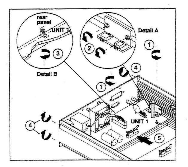
- If an IEEE-488 or RS-232 Interface is built-in remove it as described in Section 7.3.
- If a Handler Interface is built-in remove it as described in Section 7.4.
- Remove Unit 2 as described in Section 7.5.
- Unscrew two spacers (1).
- Unplug all connectors of Unit 1.
- Unscrew two screws (2) of the heatsink on the side panel as shown in Detail A.
- Unscrew the heatsink on the opposite side panel in the same way.
- Unscrew screw (3) of the fixing angle on the rear panel as shown in Detail B.
- Unscrew four screws (4) of the rear panel.
- Lift the rear panel and slide the unit to the rear (5).
7 – 3
7.7 UNIT 3, ANALOG UNIT

- Remove Unit 2 as described in Section 7.5.
- Unscrew two spacers (1) of the unit holder.
- Unscrew screw (2) of the fixing angle.
- Unplug all connectors of the unit.
- Desolder the capacitor between unit and housing.
- Slide the unit to the side panel (3).
- Remove the unit (4).
7.8 UNIT 4, KEYBOARD/DISPLAY

- Remove Unit 2 as described in Section 7.5.
- Unscrews two spacers of the unit holder of Unit 1.
- Unplug all connectors of Unit 1.
- Move Unit 1 slightly to the rear.
- Unscrews six screws (1).
- Remove Unit 4 (2) (Take care of the flexprint (3)).
7.9 UNIT 7, FLEXPRINT

Desolder the flexprint from the six banana sockets and from the 8-pole round connector.
Remove Unit 7.
7.10 UNIT 10, CONNECTOR UNIT, AND ROUND CONNECTOR

- Remove insulating pad (1).
- Desolder Connector Unit (2).
- Unscrew shielding (3).
- Unscrew nut (4).
- Remove whasher (5).
7.11 UNIT 5, DC UNIT

Unplug Unit 5 as shown in the figure.
7.12 ROD AND HOLDER FOR POWER SWITCH

- Press the clip of the rod for the power switch (1).
- Pull off the rod from the switch (2).
- Unscrew the nut from the stud on the rear panel (3).
- Pull out the holder and the switch.
7.13 POWER SWITCH

- Remove the rod for the power switch as described in Section 7.12.
- Unscrew the holder for the power switch as shown in Section 7.12.
- Bend the holder (1) to release the inner locking clips and pull out the switch (2).
7.14 TEXT PLATE
The text plate is an adhesive foil strip which cannot be reattached after you have remove it. Place a small screwdriver behind the foil strip and remove it carefully.
8
SELF DIAGNOSTIC AND TROUBLESHOOTING
In addition to the test during power on a test program is installed which checks the communication from the keyboard, the remote control interface, and the PM 9559 bin programmer as well as the data transfer to the internal memories.
The test program contains the following nine subprograms:
- Pro. I Display Test
- Pro. 2 Keyboard Test
- Pro. 3 Bin Programmer Test
- Pro. 4 Storage Register Test
- Pro. 5 EEPROM Test
- Pro. 6 Internal C-Bus Test (Strobe Test)
- Pro. 7 Measurement Data Test for Troubleshooting
- Pro. 8 Calibration Data Test
- Pro. 9 Interface Test
Press the LOCAL key, while turning the instrument on. After the power-on routine the letters tESt are shown in the display, then the menu of the test program Pro I to 9 appears. Press the LOCAL key briefly to select and carry out the test required. Press the LOCAL key again for about 1 second to return to the menu of the test program. To leave the test program, turn off the instrument.
PROGRAM 1: DISPLAY TEST
The display test checks the liquid crystal display and the respective decoders/drivers. When the text Pro. I appears in the subprogram menu, press the LOCAL key. The text REMOTE appears. Press any key. All segments of the display are switched on one after the other. You can stop and release the test with any key. The instrument then waits with the total display lit up until you press the LOCAL key to return to the menu of the test program or until you leave the test program.
PROGRAM 2: KEYBOARD TEST
This test checks the function of each key as well as those of the keyboard encoder.
Press the LOCAL key when the text Pro. 2 appears in the submenu; the display shows bCodE . If you press any key in random, the current number of this key appears in the display alone with a control number, for example, 3-00 when the AVERAGE key is pressed. This control number is generated by the keyboard encoder and can be changed to 00 , 01 , 10 , 11 by pressing this key again. The keys are numbered row by row from left to right. For example, the ZERO TRIM key has the number 8 and the STORE key has number 13.
To return to the menu of the test program, press the LOCAL key.
To leave the test program, turn off the instrument.
PROGRAM 3: BIN PROGRAMMER TEST
This test checks the function of the infrared transmitter and receiver, the function of the keys, and the encoder.
Press the LOCAL key when the text Pro. 3 appears in the submenu; the display shows ICodE . If you press any key of the bin programmer in random, the current number of this key appears in the display with a control number, for example, 4-0 when the key BINNING is pressed. This control number is generated by the encoder and can be toggled from I to 0 . The keys are numbered row by row from left to right. For example, the NOMINAL key has the number 10, and the RECALL key has the number 37.
To return to the menu of the test program, press the LOCAL key.
To leave the test program, turn off the instrument.
PROGRAM 4: MEMORY REGISTER TEST
This test checks the memory for the storage of instrument settings and trim data (ZERO TRIM). The contents of this memory are not written over or deleted during the test and can be used as usual when the test has been completed.
The test runs automatically. The display shows rEG 0 and shows PASS at the end of the test. If the test finds an error, the display shows Error .
Press the LOCAL key to return to the menu of the test program.
To leave the test program, turn off the instrument.
PROGRAM 5: EEPROM TEST
This test checks the function of the EEPROM. Press the LOCAL key when the text Pro. 5 appears. The test runs automatically. The contents of the memory is not overwritten or deleted during the test. The display shows EEPro and PASS at the end of the test. If the test finds an error the display shows Error .
Press the LOCAL key to return to the menu of the test program.
PROGRAM 6: STROBE TEST (TEST OF THE INTERNAL INTERFACE)
This test serves to test the internal data transfer to the shift registers. The outputs can be set to 'High' or 'Low' at a touch of a key.
Press the LOCAL key when the text Pro. 6 appears; the display shows C-bus and in the following submenu the numbers I to 6 .
Press any key (except LOCAL) briefly to select the strobe required. All outputs of the shift registers controlled by the selected strobe are set to 'High' or 'Low' by pressing any key.
The following table shows which shift registers are controlled by which strobe:
| Circuit Diagram |
Figure
Number |
Shift
Register |
Strobe
Number |
|---|---|---|---|
| Unit 2, Signal Synthesizer | 68 | D202 (TWS)* | 1 |
| Unit 2, Signal Synthesizer | 68 | D206 | 2 |
| Unit 3, Source | . 71 | D101 | 4 |
| Unit 3, Selector | 72 | D201 | 3 |
| Unit 3, Amplifier | 74 | D401 | 4 |
| Unit 6, Handler Interface | 84 | D106/D107 | 6 |
The TWS has internal shift registers, so you cannot measure the output. Check if the strobe line is 'High' for 1 ms when pressing a key.
Press the LOCAL key briefly to return to the strobe submenu if you want to select a different strobe line or press the key for about one second to return to the menu of the test program.
To leave the test program, turn off the instrument.
PROGRAM 7: MEASUREMENT DATA TEST
This test serves for troubleshooting in the measurement channel from the connectors to the processor.
The test has six steps which display the data during AC measurements and four steps for the optional DC measurements.
AC Measurement Data
Set the instrument to:
Test Signal Frequency 1 kHz Normal Level Continuous Mode DC Bias OFF
Check the voltage of the drive lines at the connectors on the front panel: 1 VRMS, open circuit.
Connect a resistor with 100 Ohms ± 1 % to the test posts.
Press the LOCAL key while turning the instrument on to start the test program.
Press the LOCAL key when the display shows Pro. 7.
The display shows ΠEAS (measurement) and the selected test signal frequency: FrEQ 1.0 kHz. You can select a different frequency by pressing the +/- STEP keys; for this test 1 kHz must be set.
Check the single measurements step by step by pressing any key (except LOCAL). The display shows a hexadecimal value which must be within a certain range; if the result exceeds the range perform the listed checks. Otherwise select the next step.
Press the LOCAL key to return to the menu of the test program. To leave the test program, turn off the instrument.
All stated measurement values, except the integration times of 40 ms and 50 ms, are typical values and can vary from instrument to instrument by ± 10 %.
If not stated otherwise all checks are done on Unit 3.
Vpp voltages should be measured with an oscilloscope; the signal must be a sine wave without visible distortion.
Press any key (except LOCAL and the +/-STEP keys) to start the first step.
Step 1: Voltage Measurement, Phase 0°
The display shows ITE I (first measurément) and a hexadecimal value between 38800 and 45200 Hex.
If the value exceeds the limits check the following:
N203, pin 7: Vpp = 1.4 V
If not:
- Check the connection 'Sense High' (connector on the front panel) to IC N203, pin 5.
Check the drop at diodes V232 and V233: it should be 3.4 V.
- Check diodes V230 and V231: signal must be blocked.
N207, pin 6: Vpp = 1.4 V
If not:
- Check electronical switch D204.
- Check buffers N205 and N206.
- Check differential amplifier N207 and resistor array R278.
N406, pin 6: Vpp = 3.1 V
If not:
- Check electronical switch N407.
- Check operation amplifier N406.
- Check resistors R405 to R410.
- Check relay K102 on Unit 5 (if Unit 5 is installed).
- Check jumper on X109, pins 33/34 (if Unit 5 is not installed).
N402, pin 6: Vpp = 1.6 V
If not:
- Check the 1/10 voltage divider R412, transistor array N404, switch D403, amplifier N402.
-
Check signals ABOVE and BELOW at the output of the Window Detector:
- signals must be 'High' at the end of the WDE High pulses. If not, check the Window Detector circuit.
- D501 pin13: Vpp = 1.8 V
If not
- Check the 1/4 voltage divider R426, transistor array N405, switch D404, amplifier N403.
- Signal A5 (X542): Vpp = 3.7 V
f not:
- Check 300 Hz Highpass Filter.
- Check 20 kHz Lowpass Filter.
- Check electronical switch D501.
- N603, pin 11:
VDC = -0.95 V with a superimposed AC voltage Vpp = 1.9 V, f = 2 kHz; noise caused by the digital signal is allowed.
If not:
- Check DAC N601, pin 4 (MSB), 1 kHz square wave.
- Check connection via X108 to Unit 2.
- Check operation amplifier N603.
Check the output signal NEGATIVE of the Polarity Detector: signal must be 'High' at the end of the PDE Low pulses.
N703, pin 1:
Triangle with an integration time (rise time) of: 40 ms at 50 Hz line frequency 50 ms at 60 Hz line frequency
If not:
Check the Timer Logic on Unit 2, D301 to D305.
Check the 12 MHz clock frequency.
N703, pin 1;
Triangle wave, amplitude = +2.9 V
If not:
- Check electronic switch N702.
- Check operation amplifier N703.
- Check R701 and R703 (50 Hz line frequency).
- Check R702 and R704 (60 Hz line frequency).
Check R708 to R710.
N703, pin 1: Triangle with a de-integration time (fall time) of 12 ms
If not:
- Check voltage drop at diode V706; Vpc = 4.3 V
- Check 8707.
- Check electronic switch N702.
Counter Logic on Unit 2:
- Check D308 to D312.
- Check the signal CNT_CLK: 1 = 20.97152 MHz.
- Check the serial data transfer to the microprocessor.
Step 2: Voltage Measurement, Phase +/-90°
The display shows ITE 2 (second measurement) and a hexadecimal value between 14B00 and 19500 Hex.
If the value displayed exceeds the limits check the following:
N603, pin 11: VDC = -0.15 V with a superimposed. AC voltage Vpp = 1.9 V, f = 2 kHz; noise caused by the digital signal is allowed.
If not:
- Check the output signal NEGATIVE of the Polarity Detector:
- signal must be 'High' at the end of the PDE Low pulses.
- Check whether there is a phase error in the Source Filter N101.
- Check whether there is a phase error in the 300 Hz Highpass Filter N501 or in the Lowpass Filter N502.
- Check phase switching: D208 on Unit 2.
Press any key (except LOCAL).
The display shows the gain factor and the phase setting:
| 1 |
|---|
| uAE |
Step 3: Current Measurement, Phase 0°
The display shows IE 3 (third measurement) and a hexadecimal value between 38800 and 45200 Hex.
If the value displayed exceeds the limits check the following:
N303, pin 2: Vpp = 1.4 V
If not:
- Check electronic switch N303.
- Check connection from the connector Drive Low to N301, pin 3.
- Check relay K102 on Unit 5 (if Unit 5 is installed)
- Check jumper on X109, pins 7/8 (if Unit 5 is not installed).
- N207, pin 6: Vpp 1.4 V
If not:
- Check electronic switch D204.
- Check buffer N204.
- Check connection of signals ACCH and ACCL.
Step 4: Current Measurement, Phase +/-90°
The display shows ITE 4 (forth measurement) and a hexadecimal value between 14B00 and 19500 Hex.
If the value exceeds the limits check the following:
- Check the output signal NEGATIVE of the Polarity Detector:
- signal must be 'High' at the end of the PDE Low pulses.
- Check phase switching D208 on Unit 2.
Press any key (except LOCAL). The display shows the gain factor and the phase setting:

DMAGODA
Step 5: First Reference Measurement
The display shows ΠE 5 (fifth measurement) and a hexadecimal value between 0D000 and 10000 Hex.
If the value exceeds the limits check the following:
N503, pin 6: VDC = < ±5 mV, no AC signal</li>
If not:
- Check switch D204.
- Check whether AC signals are coupled at the outputs of D204, pin 3 and pin 13.
- Check the DC offset voltages of the operation amplifiers N205 and N206.
- N703, pin 1: Triangle wave, amplitude = +0.62 V, de-integration time (fall time) 2.8 ms
If not:
Check diode voltage of V706.
- Check 8707.
- Check voltage divider R709/R710.
- Check R708.
Step 6: Second Reference Measurement
The display shows ITE 6 (sixth measurement) and a hexadecimal value between 0D000 and 10000 Hex.
The value must be the same as in step 5.
DC Measurement Data
Steps 7 to 10 are only necessary if measurements with the DC test signal are faulty. Ensure that all AC tests are within the limits. Switch the instrument off or to leave the test program. If not stated otherwise all measurements are done on Unit 5. DC voltages are measured between component and the EXT DC BIAS minus connector on the rear panel.
Set the Instrument to: Test Signal DC
Normal Level Continuous Mode
Check the voltage of the 'High Drive' line at the connectors on the front panel: +1 VDC, open circuit.
Connect a resistor with 100 Ohms ±1 % to the test posts.
Press the LOCAL key while turning the instrument on to start the test program.
Press the LOCAL key when the display shows Pro. 7. Skip steps 1 to 6 by pressing any key (except LOCAL).
Step 7: Voltage Measurement High
The display shows ITE 7 (seventh measurement) and a hexadecimal value between 38800 and 45200 Hex.
If the value exceeds the limits check the following:
N202, pin 3 (signal A1DC): VDC = +0.5 V
If not:
- Check electronic switch N202 on Unit 3.
- Check relay K202 on Unit 3.
- Check Source Overload Protector V129 to V132 on Unit 3.
- Check connectors X801/110.
-
Check X110, pin 3: VDC = < +15 mV.</li>
If not:
Check connection to the DC/V Converter N102, pin 2.
Check amplifier N102.
- Check transistor V105.
N203, pin 15: VDC = -1.5 V
If not:
- Check amplifiers N202 and N205.
- Unit 3, N406, pin 3 (signal A2): Vpp = 1.5 V, f = 2 kHz
not:
- Check DAC N203.
- Check amplifiers N206, N207, and N201.
- Check connection via relay K102 to Unit 3.
- Check latch D601 on Unit 3.
Step 8: Voltage Measurement Low
The display shows ΠE 8 (eighth measurement) and a hexadecimal value between 0C000 and 11000 Hex.
If the value exceeds the limits check the following:
N202, pin 3: VDC = <+15 mV</li>
If not:
- Check connection from the Low Sense connector on the front panel.
- Check amplifier N102.
- Check transistor V105.
N203, pin 15: VDC = 0 to -50 mV
If not:
- Check the offset voltage at the amplifiers N202 and N205.
- Check the reverse current of diodes V245 and V246 on Unit 3.
Press any key (except LOCAL).
The display shows the gain factor and the phase setting:
| [] | | |
|---|---|
| 6ud[ |
Step 9: Current Measurement High
The display shows IE 9 (ninth measurement) and a hexadecimal value between 38800 and 45200 Hex.
If the value exceeds the limits check the following:
N103, pin 3: VDC = -0.5 V
If not:
- Check amplifier N102.
- Check transistor V105.
- Check electronic switches N101 and N105.
N104, pin 6: VDC = +0.5 V
If not:
- Check amplifiers N103 and N104.
- Check resistor array R111.
Step 10: Current Measurement Low
The display shows ITE 10 (tenth measurement) and a hexadecimal value between 0C000 and 11000 Hex.
If the value exceeds the limits check the following:
N103, pin 3: VDC = <±3 mV</p>
If not:
- Check offset voltage of N102.
- Check electronic switch N101.
- N104, pin 6: VDC = <±5 mV</p>
If not:
Check offset voltages of N103 and N104.


Press the LOCAL key for about one second to return to the menu of the test program. To leave the test program, or turn off the instrument.
PROGRAM 8: CALIBRATION DATA TEST
This test displays the calculated and stored calibration factors.
Press the LOCAL key when the text Pro. 8 appears. The display shows the value and the calibration factor number, for example:

| Instrument Settings | |||||
|---|---|---|---|---|---|
| lest Signal |
Voltage
Gain |
Current
Gain |
Internal
Transresistance |
Factor
Number |
Typical
Calibration Factor (CF) |
| 1 kHz | 40 | | 1 | 100 Ω | 11 | 0.8000 to 1.2000 |
| 1 kHz | 10 | 1 | 100 Ω | 12 | 0.8000 to 1.2000 |
| 1 kHz | 1 | 1 | 100 Ω | 13 | 0.8000 to 1.2000 |
| 1 kHz | 1 | 4 | 100 Ω | 14 | 0.8000 to 1.2000 |
| 1 kHz | 1 | 10 | 100 Ω | 15 | 0.8000 to 1.2000 |
| 1 kHz | 1 | 40 | 100 Ω | 16 | 0.8000 to 1.2000 |
| 1 kHz | 40 | 1 | 10 kΩ | 21 | 0.8000 to 1.2000 |
| 1 kHz | 10 | 1 | 10 kΩ | 22 | 0.8000 to 1.2000 |
| 1 kHz | 1 | 1 | 10 kΩ | 23 | 0.8000 to 1.2000 |
| 1 kHz | 1 | 4 | 10 kΩ | 24 | 0.8000 to 1.2000 |
| 1 kHz | 1 | 10 | 10 kΩ | 25 | 0.8000 to 1.2000 |
| 1 kHz | 1 | 40 | 10 kΩ | 26 | 0.8000 to 1.2000 |
| DC | 40 | 1 | 100 Ω | 31 | 0.8000 to 1.2000 |
| DC | 10 | 1 | 100 Ω | 32 | 0.8000 to 1.2000 |
| DC | 1 | 1 | 100 Ω | 33 | 0.8000 to 1.2000 |
| DC | 1 | 4 | 100 Ω | 34 | 0.8000 to 1.2000 |
| DC | 1 | 10 | 100 Ω | 35 | 0.8000 to 1.2000 |
| DC | 1 | 40 | 100 Ω | 36 | 0.8000 to 1.2000 |
| DC | 40 | 1 | 10 kΩ | 41 | 0.8000 to 1.2000 |
| DC | 10 | 1 | 10 kΩ | 42 | 0.8000 to 1.2000 |
| DC | 1 | 1 | 10 kΩ | 43 | 0.8000 to 1.2000 |
| DC | 1 | 4 | 10 kΩ | 44 | 0.8000 to 1.2000 |
| DC | 1 | 10 | 10 kΩ | 45 | 0.8000 to 1.2000 |
| DC | 1 | 40 | 10 kΩ | 46 | 0.8000 to 1.2000 |
| 100 kHz | - | - | 10 kΩ | 51 | 0.9800 to 1.0000 |
| 100 kHz | - | - | 10 kΩ | 52 | <60 e -6 ; display 0.0000 |
| 50 Hz | - | 7 | 100 Ω | 53 | < 0.0200 |
| 50 Hz | - | - | 10 kΩ | 54 | < 0.200 |
| 100 kHz | - | - | 100 Ω | 55 | 0.9950 to 1.0050 |
The following table shows the internal settings at which the factors were calculated and the typical values. You also can compare the values with another PM6304.
Press the LOCAL key for about one second to return to the menu of the test program. To leave the test program, turn off the instrument.
Program 9: INTERFACE TEST (RS-232 or IEEE-488)
This test checks the built-in interface, its inputs and output buffers, and the correct coding and decoding of the data transferred.
Press the LOCAL key when the text Pro. 9 appears. The test automatically checks which interface is actually available; if none, noBuS appears in the display and the instrument automatically returns to the menu of the test program. In instruments with interface, there is a choice between an input test ( IdAtA ), an output test ( OdAtA ), and a read-out of the device status ( StAt ). Selection is done by pressing any key (except LOCAL). For the IEEE-488 Interface, the device address is set to 20. The configuration for the RS-232 interface is: Baud rate 9600, data bits 8, parity no. Using the RS-232 Interface the instrument must be set to remote with ESC 2.

PM6304
Input Test:
When the instrument received data via interface the display shows dAtA . The first eight figures of the string can be displayed individually in hexadecimal form by pressing any key (except LOCAL). The data input can be repeated as often as desired,

Press the LOCAL key to return to the selection between input, output, and status. Press the key again to return to the menu of the test program.
Output Test:
When the output test is selected the display shows dAtA and the identification string
'FLUKE, PM6304, 0, Vx.x'
can be read out by a controller. This test can be repeated so often as desired by pressing any key (except LOCAL).

Press the LOCAL key to return to the selection between input, output, and status. Press the key again to return to the menu of the test program.
Device-Status Test:
This test checks the data transfer from the instrument to the Standard Event Status Register and to the Status Byte Register.
Pressing any key (except LOCAL) when the display shows StAt sets the bits of the Standard Event Status Register (ESR) to 1 or 0. The display shows StAt 0 or StAt 1. If the bits of the Standard Event Status Enable Register (ESE) was set to 1 with the command *ESE 255 the controller can read out the Status Byte Register with serial poll or with the query *STB? (IEEE-488) respectively with ESC 7 for the RS-232 Interface. The result is 0 or 32 decimal, see Programmers Manual, Section 3,3. The Standard Event Status Register also can be read out by a controller with the query *ESR?

Press the LOCAL key to return to the selection between input, output, and status. Press the key again to return to the menu of the test program.
9 ERROR MESSAGES
After power on, the instrument checks the PROM, the processor RAM, and the external RAM. Additionally the instrument generates error messages if there are faults during measurements, trimming, recalibration, or if there is a fault during data transfer to a printer.
Errors are indicated as follows:
| Err 1 | Program memory checksum error |
|---|---|
| Err 2 | Processor RAM defective |
| Err 3 | External RAM defective |
| Err 4 | External RAM, backup (current instrument settings) destroyed |
| Err 5 | External RAM, stored instrument settings 1 to 9 destroyed |
| Err 6 | Error during analog to digital conversion of the test signal |
| Err 7 | EEPROM defective |
| Err 8 | Error in trim data (EEPROM) |
| Err 9 | Error in calibration data (EEPROM) |
| Err 10 | Error in binning data (EEPROM) |
| Err 11 | Error during line frequency detection |
| Err 14 | Test signal out of limits during trimming |
| Err 19 | Test signal out of limits during recalibration |
| Err 20 | Calibration factor 11 or 31 out of limits |
| Err 21 | Calibration factor 12 or 32 out of limits |
| Err 22 | Calibration factor 13 or 33 out of limits |
| Err 23 | Calibration factor 14 or 34 out of limits |
| Err 24 | Calibration factor 15 or 35 out of limits |
| Err 25 | Calibration factor 16 or 36 out of limits |
| Err 26 | Calibration factor 21 or 41 out of limits |
| Err 27 | Calibration factor 22 or 42 out of limits |
| Err 28 | Calibration factor 23 or 43 out of limits |
| Err 29 | Calibration factor 24 or 44 out of limits |
| Err 30 | Calibration factor 25 or 45 out of limits |
| Err 31 | Calibration factor 26 or 46 out of limits |
| Err 35 | Calibration factor 51 out of limits |
| Err 36 | Calibration factor 52 out of limits |
| Err 37 | Calibration factor 53 or 54 out of limits |
| Err 38 | Calibration factor 55 out of limits |
| Err 40 | Value of 100 Ω reference resistor out of range |
| Err 41 | Value of 10 kΩ reference resistor out of range |
| Err 48 | Communication error to the printer (time-out) |
| x x 0 | |
For troubleshooting hints see Chapters 4 and 8.
10 INSTALLATION INSTRUCTIONS FOR OPTIONS
10.1 PM 9548 IEEE-488 INTERFACE
The PM 9548 Interface consists of a complete circuit board with mounted IEEE-488 connector, wired connector to the RCL meter, and mounting hardware, ready for installation. The instrument is already prepared for installation.
It is only necessary to open the top cover and to install the interface as shown below. For technical data and a description of how to use the instrument via remote control, see the Programmers Manual PM6304, order no. 4822 872 10167, and the Reference Manual PM6304, order no. 4822 872 10166.
WARNING
Removing the instrument covers is likely to expose live parts, and also accessible terminals may be live. To avoid electric shock, turn off line power and remove the power cord before disassembling the instrument.
Capacitors inside the instrument may still be charged even after the instrument has been turned off or disconnected from the power supply.

- Remove 2 screws (1) from the rear bumpers.
- Remove rear bumpers (2).
- Loosen 2 screws of cover (3) (3 to 4 turns).
- Remove top cover (4).

- Remove 2 special screws (6) from the IEEE-488 connector.
- Remove 2 screws fixing the cover sheet of the slot for the IEEE-488 connector at the rear panel (1).
- Remove cover sheet (2).
- Remove nut and spring washer from the spacer (3),
- it will be used to fix the IEEE-488 Interface board (7) later on.
- Insert IEEE-488 connector into the slot (4).
- Plug in the wired connector of the interface (5) as shown.
- Fasten special screws previously removed from the connector (6).
- Fasten printed circuit board (7) on the spacer with nut and washer (3) previously removed.
- Re-assemble the instrument cover and rear bumpers in opposite sequence as shown in Figure 1.
- The IEEE-488 Interface is now ready to use.
10.2 PM 9549 RS-232 INTERFACE
The PM 9549 Interface is an option for the PM 6304 RCL Meter. It consists of a complete circuit board with mounted RS-232 connector, wired connector to the RCL meter, and mounting hardware, ready for installation.
The instrument is already prepared for installation.
It is only necessary to open the top cover and to install the interface as shown below. For technical data and a description of how to use the instrument via remote control, see the Programmers Manual PM6304, order no. 4822 872 10167, and the Reference Manual PM6304, order no. 4822 872 10166.
WARNING
Removing the instrument covers is likely to expose live parts, and also accessible terminals may be live. To avoid electric shock, turn off line power and remove the power cord before disassembling the instrument.
Capacitors inside the instrument may still be charged even after the instrument has been turned off or disconnected from the power supply.

- Remove 2 screws (1) from the rear bumpers.
- Remove rear bumpers (2).
- Loosen 2 screws of cover (3) (3 to 4 turns).
- Remove top cover (4).

- Remove 2 screws and spring washers fixing the cover sheet of the slot for the RS-232 connector at the rear panel (1).
- Remove cover sheet (2).
-
Remove nut and spring washer from the spacer (3),
- it will be used to fix the RS-232 Interface board (4) later on.
- Insert RS-232 connector into the slot.
- Plug in the wired connector of the interface (5) as shown.
- Fasten screws and washers (1) previously removed from rear panel.
- Fasten printed circuit board (4) on the spacer with nut and washer (3) previously removed.
- Re-assemble the instrument cover and rear bumpers in opposite sequence as shown in Figure 3.
- The RS-232 Interface is now ready to use.
10.3 PM 9565 DC UNIT
The PM 9565 DC Unit is an option for the PM6304 RCL Meter. It consists of a complete circuit board with mounted connector; ready for built in.
The instrument is already prepared for installation.
It is only necessary to open the top cover and to plug in the unit as shown in Figures 5 and 6.
After installation, the instrument will require recalibration. The procedure is described in the Service Manual PM6304. To recalibrate the instrument, you must have the following:
| Test Set | order no. 5322 310 32273 | ||
|---|---|---|---|
| PM 9559 Bin Programmer | * | or | |
| PM 9548 IEEE-488 Interface | or | ||
| PM 9549 RS-232 Interface | and | ||
| Service Manual | order no. 4822 872 15169 |
For technical data and a description how to measure with DC, see theProgrammers Manual PM6304order no. 4822 872 10167 and theReference Manual PM6304order no. 4822 872 10166.
WARNING
Removing the instrument covers is likely to expose live parts, and also accessible terminals may be live. To avoid electric shock, turn off line power and remove the power cord before disassembling the instrument.
Capacitors inside the instrument may still be charged even after the instrument has been turned off or disconnected from the power supply.

- Remove 2 screws (1) from the rear bumpers.
- Remove rear bumpers (2).
- Loosen 2 screws of cover (3) (3 to 4 turns).
- Remove top cover (4).

- Remove the two jumpers (1).
- Plug in the DC Unit as shown in Figure 6.
- Close instrument in opposite sequence as described in Figure 5.
- Re-assemble the instrument cover and rear bumpers in opposite sequence as shown in Figure 5.
10.4 PM 9566 HANDLER INTERFACE
The PM 9566 Interface is an option for the PM6304 RCL Meter. It consists of a complete circuit board with mounted connector, wired connector to the RCL meter, mounting hardware, ready for installation.
The instrument is already prepared for installation.
It is only necessary to open the top cover and to install the interface as shown below. For technical data and a description of how to use the Handler Interface, see the Users Manual PM6304, order no. 4822 872 10162 and the Beference Manual PM6304, order no. 4822 872 10166.
WARNING
Removing the instrument covers is likely to expose live parts, and also accessible terminals may be live. To avoid electric shock, turn off line power and remove the power cord before disassembling the instrument.
Capacitors inside the instrument may still be charged even after the instrument has been turned off or disconnected from the power supply.

- Remove 2 screws (1) from the rear bumpers. Bemove rear bumpers (2).
- Remove rear bumpers (2). Loosen 2 screws of cover (3).
- (3 to 4 turns).
- Remove top cover (4).

If an IEEE-488 or RS-232 Interface is installed, proceed as follows:
- Remove 2 screws (1) from the connector.
- Remove nut and washer of the spacer (2).
- Unplug connector (3).
- Remove interface (4).

- Remove 2 screws (1) fixing the cover sheet from the slot at the rear panel.
- Remove the cover sheet (2).
- Remove 2 screws (3) from the interface holder (4).
- Fix interface holders (4) at the rear panel with screws (1) previously removed.
- Insert plug of the interface (5) into the slot and fix the interface with screws (3) on the holders (4).
- Plug in connector (6) of the interface.
- If you have removed a built in IEEE-488 respectively RS-232 Interface refit it in opposite sequence as described in Figure 8.
- Re-assemble the instrument cover and rear bumpers in opposite sequence as shown in Figure 7.
- The Handler Interface is now ready to use.
10.5 PM 9564 19" RACK MOUNT ADAPTER
This rack mount adapter (19", 2 units high) is suited for the generators PM 5135, PM 5136, PM 5138A, PM 5139, PM 5150, and the RCL Meters PM6303A, PM6304, and PM6306; valid for instruments which have two holes in the side panels covered with plastic plates (from autumn 1992 onwards).

If necessary, unscrew feet and handle of the instrument.

For assembling use the attached fixing material:
- 6 hex-head screws M6x25
- 2 hexagonal nuts M6x25
- 4 cross-slot screws M6x25
- 6 spring washers
- 8 washers
- 4 cage-nuts
- Remove the two plastic cover plates at the right and left side panels of the instrument (1).
- Screw the distance piece (2) to the right-hand or left-hand side of the instrument with two screws M6x25, washers, and spring washers (3).
-
Screw the right and left brackets (4) to the instrument respectively to the distance piece. Use two screws M6x25 with spring washers (5) for the instrument.
- Use two screws M6x25 with spring washers (6) and two nuts with washers (7) for the distance piece.
- Clip the four cage-nuts (8) into the rack-posts (9) and fasten the instrument with four cross-slotted screws M6x25 with washers (10).
Ten holes of the distance piece are covered by a foil. You may use the holes for BNC sockets in order to connect those to rear side connections of the instrument. For this purpose perforate the cover foil. If necessary use the attached plastic spacing pieces to fix the BNC socket insulated from the housing.
Note: Take care for sufficient airflow within the rack, in order to prevent overheating the instrument.
11 CHECKING AND ADJUSTING
GENERAL INFORMATION 11 1
This chapter provides the complete adjustment procedure for the instrument. Because various control functions are interdependent, a certain order of adjustment is necessary. The procedure is therefore, presented in a sequence best suited to particular adjustment.
- Warm-up time under average conditions is 15 minutes.
- Ambient temperature (23 +1) °C
- Line voltage nominal value + 2%
- Instrument performance should be checked before any adjustment is done.
-
All limits and tolerances given in this section are calibration guides, and should not be interpreted as instrument specifications
WARNING
High voltages exist at several points inside the instrument. To avoid injury, do not touch exposed connections and components while power is on. Disconnect line power before removing protective panels, soldering, or replacing components.
11.2 RECOMMENDED TEST EQUIPMENT
| AC rms Voltmeter | Fluke 8920A |
|---|---|
| DC Voltmeter | Philips PM 2535 |
| Counter | Philips PM 6665 |
| and the second |
One of the interfaces built in:
IEEE-488 interface PM 9548 or RS-232 Interface PM 9549 Bin Programmer PM 9559 PC Personal Computer
Two single test posts, red and black, are a standard accessory with every PM6304. Test post red: 5322 264 30351 Test post black: 5322 264 30352
Test Set for 5322 310 32273 PM6304 PM6304C PM6306: for contents and details, see Section 5.2
PM6304
11.3 CHECKING AND ADJUSTING PROCEDURE
Turn the instrument PM6304 on. Set PM6304 to AUTO, 1 kHz, DC BIAS OFF, CONT, NORMAL LEVEL. Wait 15 minutes with all covers in place. Remove top cover. For measurement ground ⊥ take the rear panel EXT DC BIAS minus connector for all tests, except Section 11.3.4
11.3.1 Internal Supply Voltages
| Test | PM6304 | Adjusting | Test | Value | Value |
|---|---|---|---|---|---|
| Setting | Element | Point | to set | min. to max. | |
| 1 | see above |
Unit 1
R115 Fig. 13, 16 |
Unit 1
X104/4 Fig. 13, 16 |
DC, +15 V | 14.98 to 15.02 V |
11.3.2 Clock Frequency
| 2 | 100 kHz |
Unit 2
C210 |
Front panel + | 100 kHz |
99.999 to
100.001 kHz |
|
|---|---|---|---|---|---|---|
| Fig. 17, 19 |
11.3.3 AC Voltage
| З | 1 kHz |
Unit 3
B111 |
Front panel + | AC, 1 V rms |
0.995 to
1.005 V rms |
|
|---|---|---|---|---|---|---|
| Fig. 21, 22 |
11.3.4 DC Offset Voltage
Set PM6304 to 200 Hz and to SINGLE measurement.
Send commands via PC and interface to PM6304: BK_TEST, SET_SOURCE 3100, SET_GAIN xxx. Check that REMOTE at the front panel is lit.
Test 4 must be done before test 5 and 6.
| Test |
PM6304
setting |
Adjusting
Element |
Test
Point |
Value
to set |
Value
min. to max. |
|---|---|---|---|---|---|
| 4 |
SET_GAIN
2007 |
Unit 3
R242 Fig. 21, 23 |
A5, X542
to ⊥ X1 |
DC, 0 V | 0 ± 15 mV |
| 5 |
SET_GAIN
1007 |
Unit 3
R287 Fig. 21, 23 |
DC, 0 V | 0 ± 15 mV | |
| 6 |
SET_GAIN
3007 |
Unit 3
R333 Fig. 21, 23 |
÷ | DC, 0 V | 0 ± 15 mV |
After this press the LOCAL key.

The DC offset voltage can also be adjusted without PC and interface.
- Set PM6304 to 200 Hz, Low Level.
- Press the LOCAL key, while turning the instrument on to start the test program.
- Press the LOCAL key when the display shows Pro. 7 (Program 7).
- · Short circuit the test posts.
- Press any key except LOCAL so often until the display shows IE 5 (measurement 5).
- Perform adjustment with R242 according to Test 4.
- Press the LOCAL key twice to start the Program 7 again.
- Press any key except LOCAL so often until the display shows ΠE 2 (measurement 2).
- Perform adjustment with R287 according to Test 5.
- Press the LOCAL key twice to start the Program 7 again.
-
Remove the short circuit from the test posts.
- The following step must be performed with open measurement circuit.
- Press any key except LOCAL so often until the display shows ΠE 4 (measurement 4).
- Perform adjustment with R333 according to Test 6.
11.3.5 DC Supply Voltages
| Test |
PM6304
Setting |
Adjusting
Element |
Test
Point |
Value
to check |
Value
min. to max. |
|---|---|---|---|---|---|
| В | AUTO 1 kHz | - | Unit1 | DC, -15 V | – 14.85 to – 15.15 V |
| - | X104/7 | DC, +5 V | +4.75 to +5.25 V | ||
| 9 | - | X104/5 | DC, -5 V | -4.75 to -5.25 V | |
| 10 | - | X104/8 | DC, +5 V | +4.75 to +5.25 V | |
| 11 | X104/1 |
11.3.6 Functional Check
12
Connect resistor 100 Ω ±0.1 % via the test posts to PM6304. Set PM6304 to AUTO, 1 kHz.
| Display shows | ٠ | in upper field | : 99 to 101 Ω |
|---|---|---|---|
| E | in middle numeric field | : no display | |
| ۳ | as equivalent circuit diagram | : R symbol |
| 13 | AUTO 1 kHz | - | Front panel + | AC, 0.5 V rms | 0.495 to |
|---|---|---|---|---|---|
| 14 | AUTO 1 kHz | - | Front panel – | AC, 0 V ms |
0.505 V rms
0 to 10 mV rms |
| 15 | DC ON | - |
display as
in Test 12 |
No component connected to PM6304.
| 16 |
AUTO 20 kHz
NORMAL |
- | Front panel + | AC, 1 V rms |
0.984 to
1.016 V rms |
|---|---|---|---|---|---|
| 17 | 100 kHz | Front panel + | AC, 1 V rms |
0.92 to
1.08 V rms |
Apply 5.00 V DC to EXT DC BIAS connector at the rear.
| 18 |
AUTO 1 kHz
DC BIAS ON DC BIAS EXT CONT NORMAL |
- | Front panel + | DC, +5 V | +4.9 to +5.1 V |
|---|
11.3.7 Recalibration
Perform Recalibration according to Chapter 6 of this manual.
11.3.8 Measurement Accuracy
Make Performance Test according to Chapter 5 of this manual.
11.3.9 Dissipation Factor
Connect resistor 10 kΩ and capacitor 10 nF of the Test Set in parallel to PM6304. Set PM6304 to D. 1 kHz, CONT, NORMAL.
Test result: Display must read D = 1.58 to 1.60
11.3.10 Short-Time Deviation of Measurements
This test must be done after repair work on the analog Unit 3, or on the DC Unit 5. Connect resistor 2 MΩ ±0.5 % to PM6304.
Short-Time Deviation AC
Set PM6304 to AUTO, 1 kHz, NORMAL. Perform N = 10 succeeding measurements in SINGLE MODE and note the results Mn.
From the average result Mn = (1/N) *
For improved results, calculate the standard deviation
Test result: min.
σM = 2 kΩ max.
For calculation, please take a pocket calculator.
The measurement can conveniently be done using the PM 2272 INSPECTOR software.
If the test fails, repeat same measurements with a 10 kΩ resistor.
If now the test shows much lower deviations , replace amplifier N301 in the AC/V Converter on Unit 3, Figures 21, 24.
Short-Time Deviation DC
Set PM6304 to AUTO, DC, NORMAL.
Perform the same measurements as for AC.
If the test fails, repeat same measurements with a 10 kΩ resistor.
If now the test shows much lower deviations , replace amplifier N102 on the DC Unit 5, Figures 31 and 32.
11.3.11 Fast Mode via IEEE-488 or RS-232 Interface
Apply resistor 100 Ω ±0.01 % to PM6304. Perform FAST measurement via interface, see Programmers Manual 4822 872 10167, Section 3.5.1.6.
| Level | Frequency | Test Result |
|---|---|---|
| NORMAL | 1 kHz | 100 Ω ±0.2 %, 99.8 to 100.2 Ω |
| 0.4 kHz | 100 Ω ±0.4 %, 99.6 to 100.4 Ω | |
| 10 kHz | 100 Ω ±0.4 %, 99.6 to 100.4 Ω | |
| 5 | DC | 100 Ω ±0.2 %, 99.8 to 100.2 Ω |
11.3.12 PM 9566 Handler Interface, PM 9559 Bin Programmer
For pin assignment of the Handler Interface, Unit 6, see Users Manual 4822 872 10162 (english), 4822 872 10163 (german), or 4822 872 10164 (french), Section 4.6.3.
The outputs 1 = bin 9 to 10 = bin 0 have open collector outputs.
Connect multimeter with Diode Test, e.g. PM 2518X, to the single bin outputs:
| PM6 | 304 | | multimeter |
|---|---|
| positive to bin output | |
| negative to ground |
Program the single bin outputs via IEEE-488 or RS-232 Interface:
| BK_TE | EST | |||
|---|---|---|---|---|
| SORT | ER X | X = 0 to 9 | for bin 0 to | 9 |
| X = 10 | for FAIL | |||
| st result: | bin OFF: | multimeter | display | open, "OL |
| bin ON: | multimeter o | display | <700 mV |
If there is no interface in the PM6304, you can set the bins with the PM 9559 Bin Programmer and measure 10 resistor values out of a resistor decade, e.g. 100 Ω, 110 Ω, 120 Ω, ... You may also take only one resistor and program that value successively for bin 0 to bin 10.
b, dRt
PM 9559 Bin Programmer
Te
Press the DATA INPUT key of PM 9559.
Check response of the LCD display of PM6304:
12 SAFETY INSPECTION AND TESTS AFTER REPAIR AND MAINTENANCE IN THE PRIMARY CIRCUIT
12.1 GENERAL DIRECTIVES
- Take care that creepage distance and clearances have not been reduced.
- Before soldering, bend the wires through the holes of the solder tags or wrapp the wires round the tag in the form of an open U, or maintain wiring rigidity by using cable clamps or cable lacing.
- Replace all insulating guards and plates.
12.2 SAFETY COMPONENTS
Components in the primary circuit may only be replaced by components selected by Fluke, see also Section 13.3.
12.3 CHECKING THE PROTECTIVE GROUND CONNECTION
The correct connection and condition is checked by visual control and by measuring the resistance between the protective-lead connection at the plug and the cabinet/frame. The resistance shall not be more than 0.5 Ω. During measurement the power cord should be moved. Resistance variations indicate a defect.
12.4 CHECKING THE INSULATING RESISTANCE
Measure the insulation resistance at U = 500 Vdc between the power connections and the protective lead connections. For this purpose set the power switch to ON. The insulation resistance shall not be less than 2 MΩ; 2 MΩ is a minimum requirement at 40°C and 95 % relative humidity. Under normal conditions, the insulation resistance should be much higher (10 to 20 MΩ).
13 SPARE PARTS, Figures 13.1, 13.2
13.1 GENERAL
The PM 6304 Programmable Automatic RCL Meter is repaired preferably to component level. If the fault cannot be found at the component level, the single units can be ordered; or preferably the complete instrument can be sent to Hamburg.
Spare Parts must be ordered via Consumer Service PCS Eindhoven.
13.2 STANDARD PARTS
Electrical and mechanical parts replacements can be obtained through your local Philips organization or representative. However, many of the standard electronic components can be obtained from other local suppliers. Before purchasing or ordering replacement parts, check the parts list for value, tolerance, rating, and description.
13.3 SPECIAL PARTS
In addition to the standard electronic components, the following special components are used:
- · Components, manufactured or selected by Fluke to meet specific performance requirements.
- · Components that are important for the safety of the instrument are marked with 'S' in the parts list.
- NOTE: Both type of components may only be replaced by components obtained through your local Fluke/Philips organization or representative.
13.4 TRANSISTORS AND INTEGRATED CIRCUITS
- If removed during routine maintenance, return transistors and IC's to their original positions.
- Do not replace or switch semiconductor devices unnecessarily, because this may affect the calibration of the instrument.
- Any replacement component should be of the original type or a direct replacement. Bend the leads to fit the socket or pcb holes and cut the leads to the same lenght as on the component being replaced.
- When a part has been replaced, check the operation of the part of the instrument that may be affected.
- When reinstalling power-supply transistors, use heat-sink compound to increase the heat-transfer capabilities.
WARNING
To avoid skin irritation or injury, handle heat-sink compound with care. Avoid contact with the eyes. Wash hands thoroughly after use.
NOTE: Physical size and shape of a component may affect instrument performance, particularly at high frequencies. Always use direct-replacement components, unless it is known that a substitute will not degrade instrument performance.
13.5 STATIC-SENSITIVE COMPONENTS
This instrument contains electrical components that are susceptible to damage from static discharge. Servicing static-sensitive assemblies or components should be performed only at a static-free work station by gualified service personnel.
13.6 HANDLING MOS DEVICES
Though all our MOS integrated circuits incorporate protection against electrostatic discharges, they can nevertheless be damaged by accidental overvoltages. In storing and handling them, the following precautions are recommended.
CAUTION
To avoid electric shock testing or handling and mounting call for special attention to personal safety. Personnel handling MOS devices should wear a ground strap.
13.6.1 Storage and Transport
Store and transport the circuits in their original packing. Alternatively, you can use a conductive material or a special IC carrier that either short-circuits all leads or insulates them from external contact.
13.6.2 Testing or Handling
Personnel must wear a ground strap and work on a conductive surface (e.g., metal table top) when testing the circuits or transferring them from one carrier to another. Connect all testing and handling equipment to the same surface.
Signals should not be applied to the inputs while the device power supply is off. All unused input leads should be connected either to the supply voltage or to ground.
13.6.3 Mounting
Mount MOS integrated circuits on printed circuit boards after all other components have been mounted. Take care that the circuits themselves, metal parts of the board, mounting tools, and the person doing the mounting are kept at the same electric (ground) potential. If it is impossible to ground the printed circuit board, the person mounting the circuits should touch the board before bringing the MOS circuits into contact with it.
13.6.4 Soldering
Soldering iron tips, including those of low voltage irons, or soldering baths should also be kept at the same potential as the MOS circuits and the board.
13.6.5 Static Charges
After the MOS circuits have been mounted, the proper handling precautions should still be observed. Until the subassemblies are inserted into the complete system in which the proper voltages are supplied, the board is no more than an extension of the leads of the devices mounted on the board. To prevent static charges from being transmitted through the board wiring to the device, it is recommended that conductive clips or conductive tape is put on the circuit board terminals.
13.6.6 Transient Voltages
To prevent permanent damage due to transient voltages, do not insert or remove MOS devices (or printed circuit boards with MOS devices) from test sockets or systems with power on.
13.7 SOLDERING TECHNIQUES
Working method:
- Carefully unsolder one after the other the soldering tags of the semiconductor.
- Remove all superfluous soldering material.
- Check that the tags of the replacement part are clean and pretinned in the areas where they are to be soldered.
- Locate the replacement semiconductor exactly in its place, and solder each tag to the relevant printed conductor on the circuit board.
- NOTE: Bear in mind that the maximum permissible soldering time is 10 seconds during which the temperature of the tags must not exceed 250 °C. The use of solder with a low melting point is therefore recommended. Take care not to damage the plastic encapsulation of the semiconductor (softening point of the plastic is 150 °C).
WARNING
When you are soldering inside the instrument, it is essential to use a low-voltage soldering iron, the tip of which must be grounded to the instrument.
Suitable soldering irons should have temperature control and different types of nozzles (pin point tips), e.g., Weller Magnastat WTCP or WECP, Ersa TC 70/24V.
If a higher wattage-rating soldering iron is used on the etched circuit boards, excessive heat can cause the etched circuit wiring to separate from the board base material. In general use short-time heating with tip temperature at a small point; avoid long time heating.
13.7.1 Surface Mounted Devices (SMD) Handling and Replacement
Tools and Materials:
The removal and attachment method of SMD components mainly employs convection heating. This involves the application of hot air to the solder joints. For removing, nozzles are available for different size and shaped components. This permits the heat to be placed directly on the leads.
There are always two settings on the hot-air tool, one for temperature (50 ... 500 °C) and the other for the air flow.
Next, a mini soldering iron can be used to prepare the solder pads before attachment and to do any touchup work.
To ensure proper repair of the surface mounted devices, the following tools have been carefully selected and are therefore recommended:
- A hot-air solder tool: Leister Hot-Jet
- Nozzles for the different packages
- Micro Electronic Systems (MES) repair kit, containing dispenser, vacuum pipette and different caplettes
- Mini soldering iron station: WEPC-COD3 (regulated transformer) and Weller MLR-20 (mini soldering iron)
The following materials are recommended:
- Soldering tin, dia 0.8 mm, SnPb 60/40 with a Resin Midly Activated (RMA) flux. Ordering code: 4822 390 80133
- Solder past 026
- Non-corrosive and Resin Midly Activated (RMA) Flux-Colophony. Ordering code: 4822 390 50025
- Desolder braided wire; ordering code: 4822 321 40042
- Magnifying glass 3x ... 10x
- NOTE: The recommended Leister tools and Weller mini soldering iron can be ordered via your local dealer.
Handling SMD
Electrostatic Discharge (ESD):
All integrated circuits and many semi-conductors are susceptible to ESD. Careless handling during repair can reduce life drastically. To prevent any failure which is caused by static damage, some precautions must be taken for
- Transportation: Use static shielding bags and containers
- Working area: Use anti-static mat and wristband, connected to earth potential.
Replacement of SMD:
CAUTION
Components once removed must NOT be used again.
Fluxing and Cleaning:
For optimal soldering result, solder flux must be used to chemically clean the metals and the solder. The flux removes oxide from the metals and acts as a wetting agent. Because the use of flux can cause electrical leakage problems in high-ohmic circuits, it is important to use non-corrosive and Resin Midly Activated (RMA) flux, such as Colophony.
The flux residue left over after attachment the SMD components must be removed. To ensure proper cleaning of the board, this must be done IMMEDIATELY after repair. The longer the flux remains on the board, the harder it is to clean.
Replacement of SMDs with up to four connections
NOTE: Before removing the component, observe very carefully its position to avoid that the new component is installed upside-down. This is especially important for capacitors and four-leads SOTs.
REMOVING:
ATTENTION: Be careful that the adjacent components are not damaged by the hot-air flow.

- Prepare the hot-air tool; attach a 3 x 1.5 mm oval tip nozzle, set the temperature of the hot gas to 450 °C and the air flow to 'high'.
- Hold the nozzle 5 mm above the component to be removed.
- Heat the component up equally for about 5 seconds.
- When the solder becomes molten, remove the component from the board using the vacuum pipette.
- Remove the hot-air tool.
- Clean all pads with the braided wire.
ATTACHING:

- Apply new solder paste in small dots to all soldering pads.
- Prepare the hot-air tool; use a 3 x 1.5 mm oval tip nozzle, set the hot gas to 350 °C and the air flow to 'low'.
- Place the new component with a pair of tweezers on the sticky solder paste of the contact pads.
- Position the component well.
- Apply the heat from a distance of 5 mm in the direction of the solder paste.
- Allow even reflow of the solder, the soldering time per joint should be not more than about 10 seconds.
- Remove the hot-air tool.
- Clean the pcb very carefully; be sure to remove all flux residue.
- Inspect the solder joints and, if necessary, remove superfluous solder rests with the use of braided wire.
Replacement of SMDs with more connections
REMOVING:
ATTENTION: Be careful that the adjacent components are not damaged by the hot-air flow.

- Prepare the hot-air tool; attach the correct nozzle, set the temperature of the hot gas to 450 °C and the air flow to 'high'.
- Hold the nozzle on the component to be removed.
- Heat all connections of the component equally up for about 10 seconds.
- When the solder becomes molten, remove the component from the board using the vacuum pipette. Use a small screwdriver to break the glue bond when necessary.
- Remove the hot-air tool.
- Clean all pads with the braided wire.
ATTACHING:
NOTE: It is very helpful to use a magnifying glass having a magnification of 3 to 10 to check the correct position of all leads.

- Apply a certain amount of flux to the solder pads.
- Apply new solder paste in a straight line to the soldering pads. Prepare the hot-air tool; attach a 3 x 1.5 mm oval tip nozzle, set the temperature of the hot gas to 350 °C and the air flow to 'low'.
- Place the new component with a pair of tweezers on the sticky solder paste of the contact pads. Use the pin no. 1 location for reference.
- Fix the component with a small soldering tip by briefly heating soldering pads in two diagonally opposite corners.
- Apply the heat from a distance of 5 mm in the direction of the solder paste.
- Slowly move the nozzle over the row of solder joints.
- Allow even reflow of the solder, the soldering time per joint should be not more than about 10 seconds.
- Remove the hot-air tool.
- Clean the pcb very carefully; be sure to remove all flux residue.
- Inspect the solder joints for good connections or short-circuits and, if necessary, remove superfluous solder rests with the use of braided wire.
13.8 MAINS CABLES

North America 5322 321 10752
Universal Europe 5322 321 10755
England, U.K.
Switzerland
Australia 5322 321 10754
13 - 8
SPARE PARTS PM6304

Fig. 13.1 Mechanical parts, housing


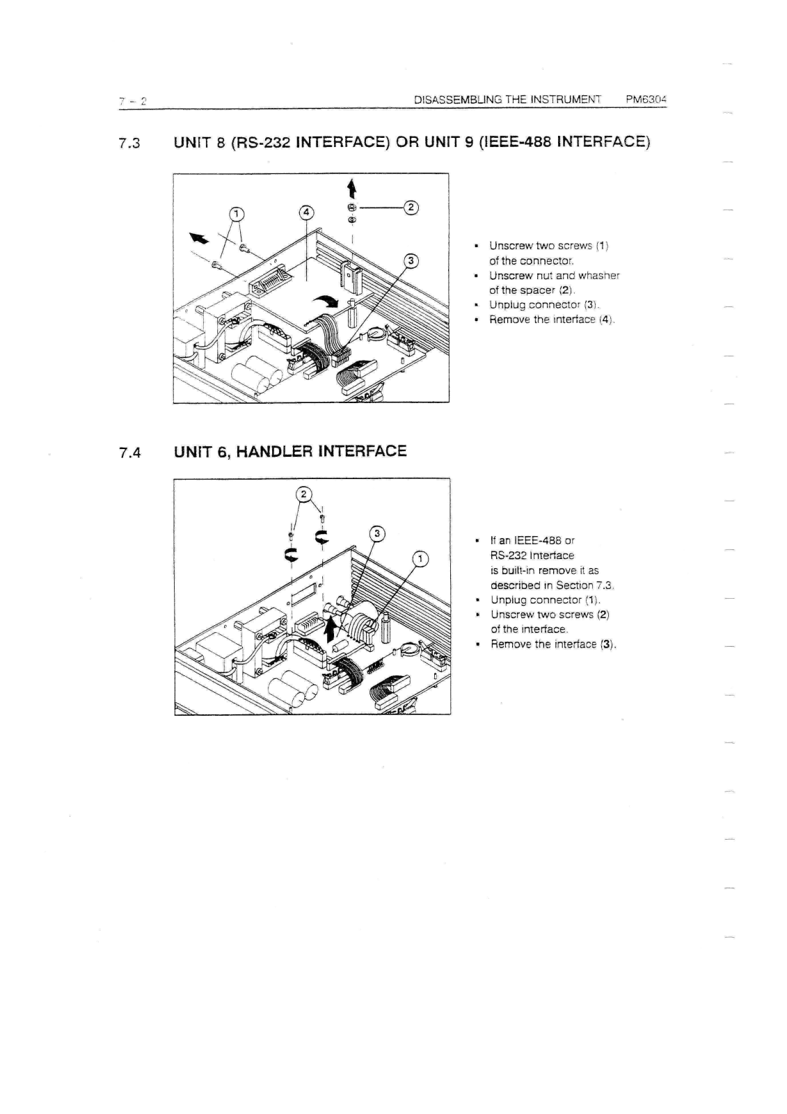


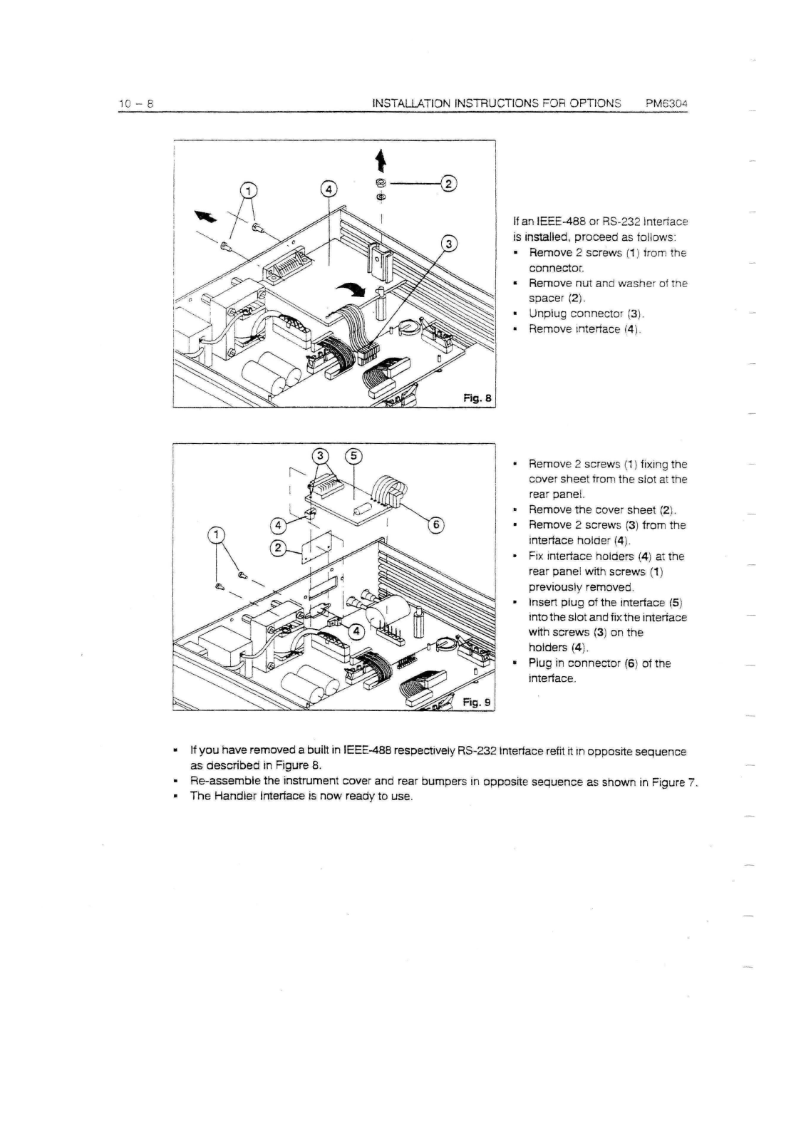


 Loading...