

Page 1

Installation, Operation, and
Maintenance
COMMUNICATIONS ISOLATOR
August 2006
Manual No.960CI-200-1 Rev. 2
©2006 Fluke Corporation, All rights reserved. Printed in U.S.A.
All product names are trademarks of their respective companies.
Model 960CI-200
Instruction Manual
Page 2

Fluke Biomedical
Radiation Management Services
6045 Cochran Road
Cleveland, Ohio 44139
440.498.2564
www.flukebiomedical.com/rms
Page 3

Table of Contents
Section 1: Introduction................................................................................................ 1-1
1.1 General Description..................................................................................... 1-1
1.2 Application................................................................................................... 1-1
1.3 Specifications............................................................................................... 1-1
Section 2: Receiving Inspection and Storage ........................................................... 2-1
2.1 Receiving Inspection.................................................................................... 2-1
2.2 Storage........................................................................................................ 2-1
Section 3: Installation.................................................................................................. 3-1
3.1 Installation.................................................................................................... 3-1
Section 4: Theory of Operation................................................................................... 4-1
4.1 Theory of Operation..................................................................................... 4-1
4.2 Address Allocation....................................................................................... 4-1
4.3 Isolator.........................................................................................................4-2
4.4 Channel ID................................................................................................... 4-2
4.5 Address Decoding ....................................................................................... 4-2
4.6 Communication Loops................................................................................. 4-2
4.7 Clock Circuitry.............................................................................................. 4-2
4.8 Baud Rate Generator................................................................................... 4-2
4.9 NMI and FNMI ............................................................................................. 4-2
4.10 Memory........................................................................................................ 4-2
Section 5: Maintenance............................................................................................... 5-1
Section 6: Calibration.................................................................................................. 6-1
Section 7:
Appendix A: Connector Designations ...........................................................................A-1
Appendix B: Applicable Drawings and Bill of Materials...............................................B-1
Figure Description Page
Figure 1-1 960CI-200 Communications Isolator Functional Block Diagram.................. 1-2
Figure 4-1 960CI-200 Loop Diagram............................................................................. 4-4
Troubleshooting ........................................................................................ 7-1
List of Figures:
(Blank page)
Page 4

Page 5

Introduction
1
Section 1
Introduction
1.1 General Description
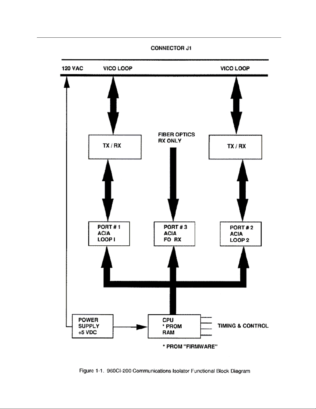
The 960CI-200 series Communications Isolator is designed for use in Victoreen’s 960 Digital Radiation Monitoring
System for Class 1E applications. Its function is to isolate the safety related monitor from a commercially rated
computer both electrically and mechanically. The monitor transmits data serially to the 960CI isolator through a fiber
optic cable. Figure 1-1 is a block diagram of the Communications Isolator Module.
1.2 Application
The 960CI-200 series Communications Isolator Module is used for communication isolation whenever a safety related
monitor needs to be connected to a computer. This isolation is for the serial asynchronous communication link. The
960CI is designed for use with the 960IC Card Cage Assembly, which holds up to 8 960CI modules.
1.3 Specifications
General specifications for the 960CI-200 Communications Isolator Module are listed below. The module (960CI-200)
is only available rated for nuclear safety-related applications. However, the module may also be used in commercial
applications.
The 960CI-200 module is assembled by techniques and with parts selected for the reliability required in a nuclear
application. Any repairs made to the nuclear rated module will void its safety-related rating. The module (960CI-200)
must be returned to the factory for authorized qualified ANSI 45.2.6, 1978, Skill
Level II service.
Specifications:
Dimensions (H x W x D) 12in x 6.5in x 1in (304.8mm x 156.2mm x 25.4mm)
Weight 1 lb., 9 oz. (708.74g)
Operating Temperature 32° to 122°F (0° to 50°C)
Relative Humidity 0 to 95% noncondensing
Power + 5 VDC @ 500mA, 115 VAC
Isolation Optical, 50 kV minimum
Processor Motorola 6809
Data Bus 8 internal data lines D0 through D7
Address Bus 16 internal address lines A0 through A15
Control & Timing 01, 02 two phase 1 MHz clock R/W, short 02 early 0 for
WRITE reset
Channel ID 32 codes, switch selectable
Communication One way optical serial line to a safety related monitor;
two way serial link to a computer
Baud Rates See Table 4-2
Memory 32K x 8 PROM, 24 x 8 RAM
1-1
Page 6
Introduction
1
1-2
Page 7

Receiving Inspection
And Storage
Section 2
Receiving Inspection and Storage
2.1 Receiving Inspection
Upon receipt of the unit:
1. Inspect the carton(s) and contents for damage. If damage is evident, file a claim with the carrier and notify
the Fluke Biomedical RMS Customer Service Department.
FLUKE BIOMEDICAL, RMS
6045 Cochran Rd.
Cleveland, OH 44139
Phone: (440) 498-2564
Fax: (440) 542-3682
www.flukebiomedical.com/rms
2. Remove the contents from the packing material.
3. Verify that all items listed on the packing list have been received and are in good condition.
NOTE
If any of the listed items are missing or damaged, notify the
Fluke Biomedical RMS Customer Service Department.
2
2.2 Storage
Storage of the Victoreen instruments must comply with Level B storage requirements as outlined in ANSI N45.2.2
(1972) Section 6.1.2(.2). The storage area shall comply with ANSI N45.2.2 (1972) Section 6.2 Storage Area, Paragraphs
6.2.1 through 6.2.5. Housekeeping shall conform to ANSI N45.2.3 (1972).
Level B components shall be stored within a fire resistant, tear resistant, weather tight enclosure, in a well-ventilated
building or equivalent.
Storage of Victoreen instruments must comply with the following:
1. Inspection and examination of items in storage must be in accordance with ANSI N45.2.2 (1972) Section
6.4.1.
2. Requirements for proper storage must be documented and written procedures or instructions must be
established.
3. In the event of fire, post-fire evaluation must be in accordance with ANSI N45.2.2 (1972), Section 6.4.3.
4. Removal of items from storage must be in accordance with ANSI N45.2.2 (1972), Sections 6.5 and 6.6.
2-1
Page 8

(Blank Page)
2-2
Page 9

Installation
Section 3
Installation
3.1 Installation
Communications Isolator Module 960CI-200 is supplied as part of a radiation monitoring system or as a
replacement part for an existing monitoring system. When the module is shipped as part of a system, it is
installed at the factory.
When a module is shipped as a replacement part, verify that jumper addresses and PROM’s are in the same
configuration as the module, which is being replaced.
3
3-1
Page 10

(Blank Page)
3-2
Page 11

Theory of Operation
4
Section 4
Theory of Operation
4.1 Theory of Operation
Figure 1-1 is the block diagram for the 960CI-200 Communications Isolator. The circuitry is explained in the following
paragraphs. Refer to the schematic diagrams in Appendix B to understand the circuit explanations.
4.2 Address Allocation
Table 4-1 lists the address allocations for the internal circuitry of the isolator.
Table 4-1. Address Allocations
Address
300 Loop 1 (to computer)
400 Loop 2 (to computer)
500 Loop 3 (from computer)
200 Channel ID
2000 – 7FFF RAM
8000 – FFFF PROM
Allocation
4.3 Isolator
Refer to schematic 960CI-200-13
REG1 is the +5 VDC power supply that provides power. The customer supplies the 120 VAC input power. SW4 is the
120 VAC power switch. Surge and spike protection is provided by D1.
Optical receiver F01 and IC U21 provides a TTL level signal to the RX input of U17. IC U17 is used strictly for receiving
(RX). The transmit (TX) line is not active or connected. The signal input for U21 is the optically isolated serial data
from the safety related monitor (SRD). Signal decoding for the communications isolator comes from U6. The
decoded instructions are used to generate the enable signals for the three communication ports.
4.4 Channel ID
SW3 is an array of 6 switches that are used to set the channel identification code. It can be set from 00 HEX to 3F HEX
(64 settings). U15 is an octal buffer chip with a 3 state output. It is enabled for reading the CHANNEL ID.
When U7 receives a READ instruction, data will be transferred to the microprocessor.
4-1
Page 12

Theory of Operation
4
4.5 Address Decoding
The address decoding is done by U9, U8, U11, and U6. Logic array U6 is programmed to provide the following enable
signals:
ACIA1 - for address 300 through 3FF
ACIA2 - for address 400 through 4FF
ACIA3 - for address 500 through 5FF
RAM1 - for memory RAM 2000 – 3FFF
RAM2 - for memory RAM 4000 – 5FFF
RAM3 - for memory RAM 6000 – 7FFF
PROM - for memory PROM 8000 – FFFF
U6 provides a control signal to the internal data bus transceiver to route data to and from memory to the processor.
Under a READ command the processor reads from memory. Under a WRITE command the processor writes to
memory. U9 provides the CHAN ID signal that enables U15 and read the channel identification.
4.6 Communication Loops
The 960CI-200 has three communication loops. Loops 1 and 2 are used for two-way communications with the
computer, while loop 3 is a receive only one-way communications loop to the monitor.
Only loop 1 will be discussed here since loop 2 circuitry is identical in operation. (ACIA1, U16 is loop 1) & (ACIA2, U17
& Z9 is loop 2). The ACIA’s have the following signal inputs and outputs:
CONTROL: T2 L02 R/W, A0, UB BIT RATE, ACIA 1,2,3, IRQ, and UB BIT RATE (determines data baud rate)
DATA: Parallel D0 through D7, Serial TX & Serial RX, T2, 02. All data transfers occur on falling edge
of 02.
R/W: HI for read and LO for write operations.
A0: Part of the address decoding, A0 = 0 for data and A0 = 1 for control
ACIA 1,2,3: Selected when low
IRQ: Output that goes to the processor to cause an interrupt when receiving data and the
buffer is full.
D0 – D7: Parallel data bus (internal data bus)
TX: Transmit (Serial data)
4-2
Page 13

Theory of Operation
4
RX: Receive (Serial data)
When address 300 is decoded, ACIA1 goes low and enables U16. Data can then be READ from or WRITTEN to the
ACIA. For detailed operation of a 6850 ACIA refer to the Motorola manual.
U19 is a watchdog timer for the time-out circuit. IC U9 is a dual re-triggerable one-shot chip. It is trailing edge
triggered and has a fixed output of 100 ms. when timed out, Q1 will be high and LOOP 1 TX DATA will be high also.
This condition is necessary because LOOP 1 TX could be low at that time due to a condition on ACIA 1, which could
cause it to latch low. During the next transmission, transistor Q1 will be low and LOOP 1 TX will pass through OR gate
U20.
Serial data is communicated between two monitors or between a monitor and a minicomputer through connector
J2. Refer to figure 4-1 for the loop diagram.
Zener diode D6 and resistor R24 regulate the voltage to the 5 VDC required to operate the optical isolator’s transistor,
(part of U22). The +VL1 and –VL1 voltage for the communication loop is a floating 30 VDC. +VL2 voltage equals + 15
VDC and –VL2 equals –15 VDC. When the signal LOOP 1 TX DATA is low (logic 0), transistor Q3 turns on. As Q3
conducts, it supplies +5 VDC to pin 1 of U22 turning on the LED. This will cause the transistor in U22 to turn on.
U22’s output at pin 5 will go low (toward –VL, -15 VDC), causing transistor Q5 to turn off. When Q5 is turned off, its
output at the collector goes high. This will turn on both Q7 and Q11. Q11 conducts and TX-1 line will be pulled to –
VL1. Transistor Q7 also conducts, causing Q9 to turn on. This pulls TX+1 to +VL1.
When the LOOP 1 TX DATA signal is high, the process is reverted. The voltages at TX+1 and TX-1 will in effect change
polarity. The TX-1 goes to VL+1 and TX+1 goes to VL-1 through resistors R42 and R44.
The RX section of the loop receives a signal from a transmit loop. When RX+ is at –VL and RX- is at +VL, U24 will be
on to transmit logic 0 to ACIA 1 through LOOP 1 RX DATA. When RX+ is at +VL and RX- is at –VL, U24 will be off and
ACIA 1 will receive logic 1 (R48 is a pull-up resistor to +5 VDC).
4.7 Clock Circuitry
XTAL 1 is a 4 MHz crystal from which the basic clock frequency is derived. Pin 34 of U1 is used for TTL 02. U9 and U8
generate SHORT 02, which is used for early write in a write cycle.
4.8 Baud Rate Generator
U12 is a CMOS programmable bit rate generator. Base crystal frequency is 2.4576 MHz, connected between pins 6
and 7. Output is at pin 10. Bit rate programming is done by switch setting on SW2 (refer to table 4-2 for baud rate
selection). Pin 15 and pin 3 are shorted and give a base frequency of 302700 Hz to generate NMI and FNMI signals.
4-3
Page 14

Theory of Operation
4
Table 4-2. Baud Rate Settings
SW2
(Baud Rate)
110.0 OP OP OP OP
150.0 OP OP OP CL
300.0 OP OP CL OP
2400.0 OP OP CL CL
1200.0 OP CL OP OP
1800.0 OP CL OP CL
4800.0 OP CL CL OP
9600.0 OP CL CL CL
600.0 CL OP OP CL
50.0 CL CL OP CL
75.0 CL CL OP OP
200.0 CL OP CL OP
134.5 CL OP CL CL
NOTE: OP = Open CL = Closed
4.9 NMI and FNMI
Pin 1 to 8
(S3)
Pin 2 to 7
(S2)
Pin 3 to 6
(S1)
Pin 4 to 5
(S0)
Clock generator U13 is a CMOS programmable bit rate generator that gets 302700 Hz at its CP (pin 5) input and is set
with S0 = high, S1 = low, S2 = high, and S3 = low to generate a frequency output at pin 10 that is sent to dual decade
counter U14. U14 pin 7 has 4 Hz NMI, while pins 12 & 13 have 100 Hz FNMI.
4.10 Memory
The 960CI-200 Communications Isolator has 32K of memory using one 32K x 8 chip. One memory socket is used for a
PROM (address 8000 through FFFF) and three sockets are used for RAM memory (address 2000 through 7FFF). When
memory is accessed, U6 will have four chips enable signals (CE) on its output, depending on the address as shown in
table 4-3.
Table 4-3. Address Decoding For Memory
Address
2000 – 3FFF 0 0 0 RAM 1 0 1 1
4000 – 5FFF 0 0 1 RAM 1 1 0 1
6000 – 7FFF 0 1 0 RAM 1 1 1 0
8000 – FFFF 1 0 1 PROM 0 1 1 1
ICs U3, U4, U5 are RAM and U2 is PROM.
A13
A12
A11
TYPE
Line
PROM
RAM 1
RAM 2
RAM 3
4-4
Page 15

Theory of Operation
4
4-5
Page 16

(Blank Page)
4-6
Page 17

5.1 Maintenance
No periodic maintenance is required for this module.
If a maintenance question arises and cannot be resolved by using
this manual, please contact the Fluke Biomedical RMS Customer
Service Department at (440) 498-2564 for assistance.
Maintenance
5
Section 5
Maintenance
NOTE
5-1
Page 18

(Blank Page)
5-2
Page 19

6.1 Calibration
The 960CI-200 module does not require any calibration.
(Blank Page)
Calibration
6
Section 6
Calibration
6-1
Page 20

6-2
Page 21

Troubleshooting
7
Section 7
Troubleshooting
7.1 Troubleshooting
WARNING
Extreme care must be used when troubleshooting a system that
has power applied. All standard troubleshooting precautions
apply.
WARNING
Once a problem has been located, remove all power before
continuing with the repair.
CAUTION
Personnel performing the following procedure must be familiar
with the operation of the monitoring system and the location of
each piece of equipment used in the system.
If a problem develops, verify that the voltages at connection point inputs and outputs are present and that all wiring
is secure. Refer to Appendix B for drawings.
The 960CI-200 Communications Isolator Module must be returned to the factory for service if troubleshooting of the
module is necessary.
NOTE
If a problem cannot be resolved by using the drawings in
Appendix B while applying the troubleshooting instructions found
in this manual, please contact the Fluke Biomedical RMS Customer
Service Department at (440) 498-2564 for assistance.
(Blank Page)
7-1
Page 22

7-2
Page 23

Appendix
Connector Designations
A
Appendix A
Connector Designations
J2 PIN DESIGNATION
Pin
1 Line (120 VAC) 14 Line (120 VAC)
2 Neutral (120 VAC) 15 Neutral (120 VAC)
3 Ground (chassis) 16 Ground (chassis)
4-7 Not Used 17-19 Not Used
8 -VL1 20 -VL2
9 +VL1 21 +VL2
10 -RX1 22 -RX2
11 +RX1 23 +RX2
12 -TX1 24 -TX2
13 +TX1 25 +TX2
Description
Pin
Description
(Blank Page)
A-1
Page 24

Appendix
Applicable Drawings
And Bill of Materials
B
Appendix B
Applicable Drawings
DRAWINGS:
BILL OF MATERIALS:
DRAWING DESCRIPTION
960CI-200-13 Schematic Diagram, Communications Isolator Module
960CI-200-10 Communications Isolator Module Printed Circuit Assembly
DOCUMENT DESCRIPTION
960CI-200-10 Bill of Materials, Communications Isolator Module Printed Circuit
And Bill of Materials
Assembly
B-1
Page 25

Fluke Biomedical
Radiation Management Services
6045 Cochran Road
Cleveland, Ohio 44139
440.498.2564
www.flukebiomedical.com/rms
 Loading...