

Page 1

Installation, Operation, and
Maintenance
Instruction Manual
Wide-Range Area Monitoring
System
Model 945A
April, 2006, P/N 945A-1, Rev. 13
©2006 Fluke Corporation, All rights reserved. Printed in U.S.A.
All product names are trademarks of their respective companies
Page 2

Fluke Biomedical
Radiation Management Services
6045 Cochran Road
Cleveland, Ohio 44139
440.498.2564
www.flukebiomedical.com/rms
ii
Page 3

PROCEDURES, WARNINGS, AND CAUTIONS
The equipment described in this manual is intended to be used for the detection and measurement of
ionizing radiation. It should be used only by persons who have been trained in the proper interpretation of
its readings and the appropriate safety procedures to be followed in the presence of radiation.
Although the equipment described in this manual is designed and manufactured in compliance with all
applicable safety standards, certain hazards are inherent in the use of electronic and radiometric
equipment.
WARNINGS and CAUTIONS are presented throughout this document to alert the user to potentially
hazardous situations. A WARNING is a precautionary message preceding an operation which has the
potential to cause personal injury or death. A CAUTION is a precautionary message preceding an
operation which has the potential to cause permanent damage to the equipment and/or loss of data.
Failure to comply with WARNINGS and CAUTIONS is at the user's own risk and is sufficient cause to
terminate the warranty agreement between Fluke Biomedical RMS and the customer.
Adequate warnings are included in this manual and on the product itself to cover hazards that may be
encountered in normal use and servicing of this equipment. No other procedures are warranted by Fluke
Biomedical RMS. It shall be the owner's or user's responsibility to see to it that the procedures described
here are meticulously followed, and especially that WARNINGS and CAUTIONS are heeded. Failure on
the part of the owner or user in any way to follow the prescribed procedures shall absolve Fluke
Biomedical RMS and its agents from any resulting liability.
Indicated battery and other operational tests must be performed prior to each use to assure that the
instrument is functioning properly. If applicable, failure to conduct periodic performance tests in
accordance with ANSI N323-1978 (R1983) Radiation Protection Instrumentation Test and
Calibration, paragraphs 4.6 and 5.4, and to keep records thereof in accordance with paragraph 4.5 of
the same standard, could result in erroneous readings or potential danger. ANSI N323-1978 becomes,
by this reference, a part of this operating procedure.
READ YOUR INSTRUCTION MANUAL
iii
Page 4

iv
Page 5

Table of Contents
Page
SECTION 1 - INTRODUCTION........................................................................................................................... 1-1
G
ENERAL DESCRIPTION....................................................................................................................................... 1-1
Ion Chamber Detector/Preamplifier, Model 977-210....................................................................................... 1-1
Specifications, Ion Chamber Detector............................................................................................................... 1-2
Specifications, Preamplifier, Model 977-210-95 ............................................................................................... 1-2
Universal Digital Ratemeter, Model 946A-200................................................................................................. 1-4
Application ..........................................................................................................................................................................1-5
Specifications .......................................................................................................................................................................1-5
Auxiliary Equipment........................................................................................................................................... 1-6
SECTION 2 - RECEIVING INSPECTION AND STORAGE............................................................................ 2-1
R
ECEIVING INSPECTION....................................................................................................................................... 2-1
S
TORAGE ................................................................................................................................................................. 2-1
SECTION 3 - INSTALLATION............................................................................................................................ 3-1
I
NSTALLATION ....................................................................................................................................................... 3-1
Detector Mounting............................................................................................................................................... 3-1
UDR Mounting .................................................................................................................................................... 3-1
E
LECTRICAL INTERFACE..................................................................................................................................... 3-2
S
ET-UP...................................................................................................................................................................... 3-6
SECTION 4 - OPERATION/FUNCTIONAL DESCRIPTION.......................................................................... 4-1
O
PERATION............................................................................................................................................................. 4-1
D
ETECTOR OPERATION........................................................................................................................................ 4-1
UDR O
PERATION / FUNCTIONS........................................................................................................................... 4-3
Normal Operation ............................................................................................................................................... 4-3
WARN/HIGH Alarms......................................................................................................................................... 4-3
Range Alarm........................................................................................................................................................ 4-3
Fail Alarm ............................................................................................................................................................ 4-4
Check Source ....................................................................................................................................................... 4-4
F
IRMWARE VERSION............................................................................................................................................. 4-4
O
PERATIONAL MODES.......................................................................................................................................... 4-5
Rate Mode (Normal Operation)......................................................................................................................... 4-5
Data Entry Mode................................................................................................................................................. 4-5
Alarm Inhibit....................................................................................................................................................... 4-5
Check Source ....................................................................................................................................................... 4-5
Maintenance Mode.............................................................................................................................................. 4-6
Auto Zero Mode................................................................................................................................................... 4-7
Loop Test Mode................................................................................................................................................... 4-7
A
LARMS................................................................................................................................................................... 4-7
Alarm Logic ......................................................................................................................................................... 4-7
Manual Reset....................................................................................................................................................................... 4-8
Auto Reset............................................................................................................................................................................4-8
HIGH Alarm........................................................................................................................................................ 4-8
WARN Alarm ...................................................................................................................................................... 4-8
RANGE Alarm..................................................................................................................................................... 4-9
v
Page 6

Table of Contents
Page
FAIL Alarms........................................................................................................................................................ 4-9
Low Signal Failure..............................................................................................................................................................4-9
Auto Zero Failure .............................................................................................................................................................4-10
High Voltage Failure.........................................................................................................................................................4-10
Loop Failure......................................................................................................................................................................4-10
Power Failure.................................................................................................................................................................... 4-10
MPU Failure ......................................................................................................................................................................4-10
POWER UP PROCEDURE ..................................................................................................................................... 4-11
H
OW TO ENTER SETPOINTS............................................................................................................................... 4-11
S
ETPOINT DESCRIPTIONS................................................................................................................................... 4-12
HIGH Alarm Limit............................................................................................................................................ 4-12
WARN Alarm Limit.......................................................................................................................................... 4-12
Overrange Limit................................................................................................................................................ 4-12
Underrange Limit.............................................................................................................................................. 4-13
Analog Full Scale............................................................................................................................................... 4-13
Calibration Factor............................................................................................................................................. 4-13
Analog Low Scale .............................................................................................................................................. 4-13
S
ET POINT ERROR CODES.................................................................................................................................. 4-13
A
NALOG OUTPUT................................................................................................................................................. 4-14
V
ICTOREEN COMMUNICATIONS LOOP............................................................................................................ 4-15
(P
REAMPLIFIER SWITCH & JUMPER SETTINGS) ........................................................................................... 4-15
D
IGITAL RATEMETER CONFIGURATION OPTIONS ....................................................................................... 4-16
UDR S
WITCH AND TABLE SETTINGS................................................................................................................ 4-16
Jumper Selectable Options............................................................................................................................... 4-16
UDR Function Switch / Function..................................................................................................................... 4-17
E
RROR CODES ...................................................................................................................................................... 4-17
P
REAMPLIFIER/UDR DIAGNOSTIC LED INDICATORS.................................................................................. 4-18
977-210 Detector/Preamplifier ......................................................................................................................... 4-18
946A-200 UDR................................................................................................................................................... 4-18
F
UNCTIONAL DESCRIPTION............................................................................................................................... 4-19
Detector and Preamplifier ................................................................................................................................ 4-19
Universal Digital Ratemeter (UDR), Model 946A-200................................................................................... 4-23
Main Circuit Board...........................................................................................................................................................4-23
Microprocessor............................................................................................................................................................. 4-23
Reset Circuitry.............................................................................................................................................................. 4-28
Clocks ............................................................................................................................................................................4-28
NMI Clock..................................................................................................................................................................... 4-28
Write Cycle Clock.........................................................................................................................................................4-28
Address Drivers............................................................................................................................................................ 4-28
Data Transceivers.........................................................................................................................................................4-29
Control Signal Buffer................................................................................................................................................... 4-29
Address Decoding.........................................................................................................................................................4-29
PROM............................................................................................................................................................................ 4-30
RAM ..............................................................................................................................................................................4-30
E2............................................................................................................................. ...................................................... 4-30
Read - Write Cycles..................................................................................................................................................... 4-31
Write Register Decoding..............................................................................................................................................4-31
Counter Control (Write Only)................................................................................................................................ 4-31
Relay Control Register (Write Only)......................................................................................................................4-32
Bargraph (Write Only)............................................................................................................................................4-32
Status Indicators (Write Only)................................................................................................................................4-33
Display Control (Write Only)..................................................................................................................................4-34
Digital to Analog Converter and Output Circuitry (Write Only)............................................................................4-35
vi
Page 7

Read Register Decoding...............................................................................................................................................4-35
Data Entry (Read Only)...........................................................................................................................................4-36
Sensitivity Select (Read Only).................................................................................................................................4-36
Switch Inputs............................................................................................................................................................ 4-37
Option Board Bus.........................................................................................................................................................4-38
Relay Circuit Board.......................................................................................................................................................... 4-38
Front Panel Circuit Board ...............................................................................................................................................4-38
Circuit Description (Front Panel Circuit Board).......................................................................................................4-38
Power Supply.....................................................................................................................................................................4-40
Optional Circuit Boards...................................................................................................................................................4-40
SECTION 5 - MAINTENANCE............................................................................................................................ 5-1
M
AINTENANCE 946A-200...................................................................................................................................... 5-1
R
EPLACEMENT PARTS ...................................................................................................................................... 5-1
M
AINTENANCE 977-210......................................................................................................................................... 5-1
R
EPLACEMENT PARTS ...................................................................................................................................... 5-1
SECTION 6 - CALIBRATION.............................................................................................................................. 6-1
C
ALIBRATION (INCLUDES FACTORY CAL., TEST, & TERMINATION PROCEDURES) ........................................... 6-1
SECTION 7 - TROUBLESHOOTING.................................................................................................................. 7-1
T
ROUBLESHOOTING.............................................................................................................................................. 7-1
Troubleshooting / Adjustments.......................................................................................................................... 7-2
Error Codes E0011 & E0012.............................................................................................................................. 7-2
Auto-Zero Adjustment Procedure..................................................................................................................... 7-3
Analog Output Adjustments (946A UDR) ........................................................................................................ 7-5
0 to 10 Volt, zero, and span adjust..................................................................................................................... 7-5
4 - 20 mA Analog Output Adjustment............................................................................................................... 7-6
977-210 Detector Analog Output Adjustments................................................................................................. 7-6
APPENDIX A. - CONNECTOR DESIGNATIONS ......................................................................................... 8-1
APPENDIX B. - APPLICABLE DRAWINGS.................................................................................................. 9-1
APPENDIX C. - BILL OF MATERIALS........................................................................................................ 10-1
APPENDIX D. - COAXIAL CABLE TERMINATION INSTRUCTIONS.................................................. 11-1
APPENDIX E. - COMMUNICATIONS OPTION BOARD MANUAL....................................................... 12-1
APPENDIX F. - SUPPLEMENTAL DATA (CUSTOMER SPECIFIC)...................................................... 13-1
vii
Page 8

List of Figures
Page
Figure 1-1. Detector Energy Response........................................................................................... .............................. 1-3
Figure 1-2. Front Panel, Model 946A-200 Universal Digital Ratemeter......................................................................1-6
Figure 4-1. Detector Electronics Block Diagram........................................................................................................4-22
Figure 4-2. Page 1 of 3. Block Diagram - Main Circuit Board .................................................................................. 4-24
Figure 4-3. Read / Write Timing Diagram..................................................................................................................4-27
Figure 4-4. Write Cycle Clock Timing Diagram........................................................................................................ 4-28
Figure 4-5. Front Panel, Model 946A-200.................................................................................................................. 4-39
List of Tables
Page
Table 3-1. Rear Panel Connections .............................................................................................................................3-2
Table 3-2. Connector P1 - Input/Output......................................................................................... ............................. 3-3
Table 3-3. Connector P2 - Detector Connector ........................................................................................................... 3-4
Table 3-4. Connector P3 - Power Input.......................................................................................................................3-4
Table 3-5. Connector P6 - Auxiliary I/O..................................................................................................................... 3-5
Table 3-6. Connector P7 - RS232C .............................................................................................................................3-5
Table 4-1. Response Time........................................................................................................................................... 4-2
Table 4-2. Setpoints...................................................................................................................................................4-12
Table 4-3. Preamplifier Interface Board 977-210-10 Switch Settings.......................................................................4-15
Table 4-4. Jumper Positions for Preamplifier Interface Board 977-210-10...............................................................4-15
Table 4-5. Jumper Positions for Preamplifier Electrometer Board 977-200-15 ........................................................4-15
Table 4-6. Model 946A-200 Option Jumpers............................................................................................................ 4-16
Table 4-7. UDR Function Switch Positions/Function ............................................................................................... 4-17
Table 4-8. Model 946A-200 Error Codes.................................................................................................................. 4-17
Table 4-9. Preamplifier Register Addresses ..............................................................................................................4-19
Table 4-10. Electrometer Control Bit Assignments.....................................................................................................4-20
Table 4-11. Output Signals (U14) ...............................................................................................................................4-29
Table 4-12. U1 Outputs............................................................................................................................................... 4-30
Table 4-13. Write Register Functions.......................................................................................................................... 4-31
Table 4-14. Counter Control Register Write Functions............................................................................................... 4-31
Table 4-15. Relay Control Register Write Functions..................................................................................................4-32
Table 4-16. Bargraph Write Address........................................................................................................................... 4-32
Table 4-17. Status Indicator Write Functions.............................................................................................................. 4-33
Table 4-18. Hex Data (Written to Address 4008).................................................................................
Table 4-19. Control Signal Address Decoding (U34)..................................................................................................4-35
Table 4-20. Data Entry Read Functions ...................................................................................................................... 4-36
Table 4-21. Function Switch Logic.............................................................................................................................4-36
Table 4-22. Sensitivity Select Read Functions............................................................................................................ 4-37
Table 4-23. Switch Input Bit Assignments (U62) ....................................................................................................... 4-37
Table 6-1. Electronic Adjustments ..............................................................................................................................6-1
.......................4-34
viii
Page 9

Section 1 - Introduction
General Description
The Victoreen Model 945A is a wide-range area monitoring system with a detectable range of 10-1 to 107
mR/h. The system is comprised of the Model 977-210 Ion Chamber Detector, with local preamplifier, and
a Model 946A-200 Universal Digital Ratemeter (UDR). The detector and preamplifier are connected by
two five foot cables, encased in a flexible conduit. Other cable lengths, of up to 100 feet between
preamplifier and detector, are available. Both the detector and preamplifier are wall mounted in an area
designated by the customer. The 946A-200 Universal Digital Ratemeter is mounted in a rack in the
control room. A more detailed description of each piece of equipment can be found in the following
paragraphs.
Ion Chamber Detector/Preamplifier, Model 977-210
Ion chamber detectors are similar to capacitors, with two electrodes separated by a volume of air. In
order to operate, an electrical potential is applied between the electrodes. Thus, one electrode will have
a positive charge and the other a negative charge (relative to each other). Incident ionizing radiation will
cause the air in the volume between the electrodes to dissociate into positive and negative ions. Each
ion will be attracted to the electrode of opposite polarity. Ions that reach the electrode result in charge
transfer. The charge transfer causes a current to flow in the connecting wiring, representing the
measured amount of radiation intensity experienced by the ion chamber.
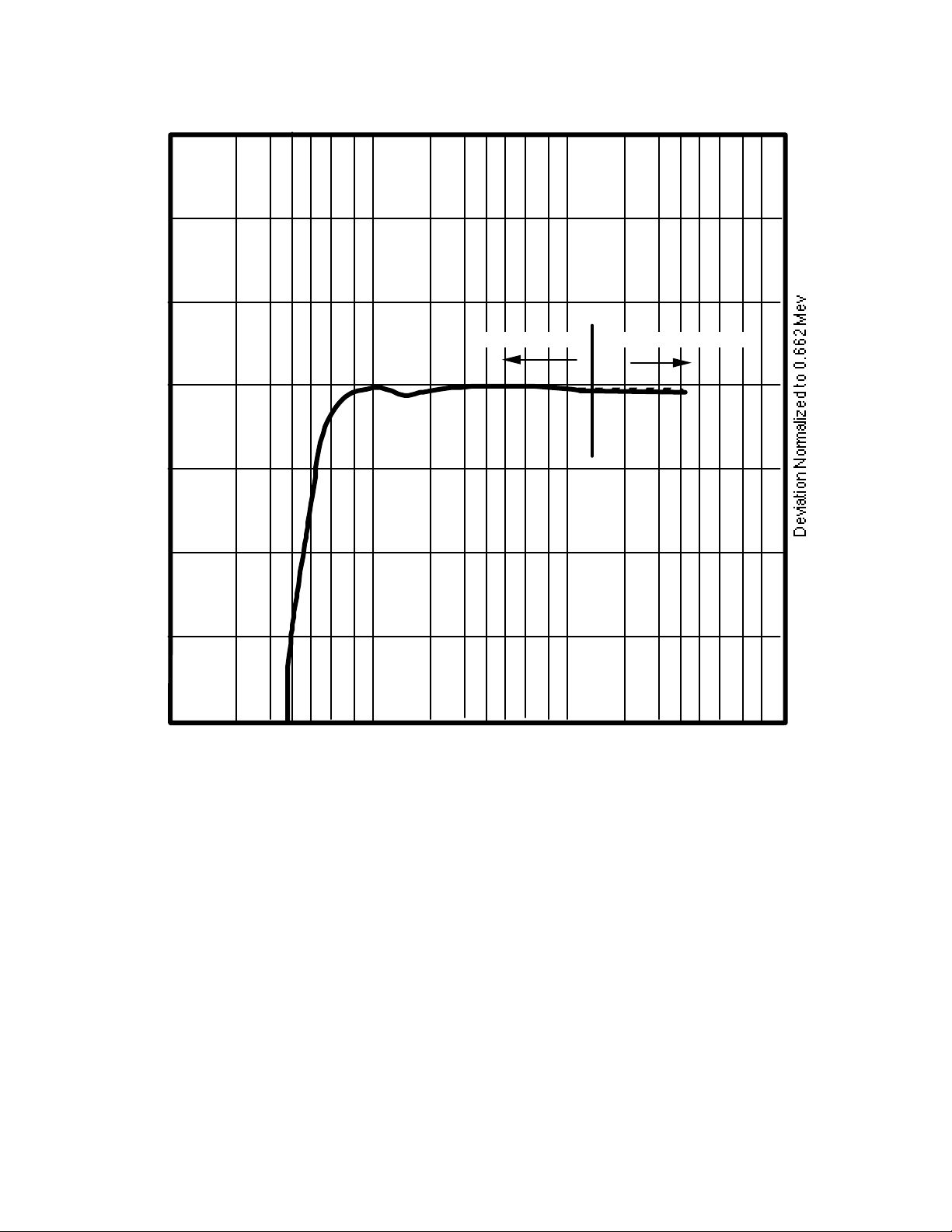
The Model 977-210 Wide-Range Ion Chamber Detector is a gamma sensitive radiation detection device,
which measures radiation in the range of 1 x 10⁻¹ mR/h to 1 x 10⁷ mR/h with an energy dependence of
less than ± 10% from 60 keV to 3 MeV. The pre-amp is housed in a gasket sealed enclosure.
Interconnection between the detector and pre-amplifier is accomplished via two five foot cables, encased
in a flexible conduit.
The wide range ion chamber detector design includes a single ion chamber with a volume of
approximately 1000 cc. The chamber walls are made of tissue equivalent plastic. An outer wall, made of
aluminum, is provided to protect the ion chamber and to mechanically interface with Victoreen’s Model
848-8 Field Test Source. The ion chamber is biased at a nominal 500 volts and produces an output
current proportional to radiation absorbed in the chamber. The current is approximately 8 x 10
The ion chamber assembly makes use of a double seal design, where the actual ion chamber is back
filled with nitrogen at atmospheric pressure. The connector area is sealed against moisture and
particulate through the use of a sealed, liquid tight flexible conduit between the detector and preamplifier
electronics.
The preamplifier contains a microprocessor controlled, auto-zeroing, integrating electrometer, a
programmable gain amplifier, an analog - to - digital converter, an asynchronous serial communications
interface, an electronic check source, and the detector high voltage power supply. Communications with
the UDR is accomplished via the optically isolated Victoreen Serial Communication Loop driver/receiver
circuitry.
-11
A/R/h.
1-1
Page 10

Specifications, Ion Chamber Detector
Detector Type
Detector Volume
Detector Constant
Detector Capacitance
Inner Chamber Gas
Radiation Detected
Detectable Range
Energy Dependence
Accuracy
Power Requirement
Check Source
Dimensions (H x W x D)
Housing
Weight
Operating Temperature
Storage Temperature
Relative Humidity
Max. External Pressure
Ionization chamber
Approximately 1000 cc
Approximately 8 x 10
30 Picofarads nominal
Dry nitrogen @ atmospheric pressure
Gamma and X-Ray
1 x 10⁻¹ to 1 x 10⁷ mR/h
± 10% from 60 keV to 3 MeV (Refer to Figure 1-1)
± 15% of true dose for Cs-137
Approximately 500 VDC; high voltage level verified
through auto-check routine
Electronic check source actuated from UDR front panel
10.31 in. x 10.5 in. x 10.5 in.
(26.19 cm x 26.67 cm x 26.67 cm)
Outer chamber protective cover is aluminum. Inner
chambers are conductive, tissue equivalent, plastic
11 lb. (5 kg)
0o to 130o F (-16o to 54o C)
0o to 132o F (-16o to 56o C)
0 to 95% non-condensing
15 psig
Specifications, Preamplifier, Model 977-210-95
Housing
Interface to detector
Interface to Readout
Interface Cable Requirement
Power Requirement
Auxiliary Alarm Output
Auxiliary Analog Output
Dimensions (H x W x L)
Weight
Operating Temperature
Storage Temperature
Relative Humidity
Electronics Life Expectancy
Steel, NEMA 4 type
Approximately 5 feet of signal cable and high voltage
cable contained within a flexible conduit. (Other lengths
available).
Victoreen Comm Loop interface to 942A UDR through
Model 942-200-80 Communications Board. Capable of
driving up to 3000 feet of cable at 4800 Baud.
Seven (7) conductors, 16 AWG for maximum
preamplifier/readout distance, excluding local alarm
requirements
+15 Vdc @ 250 mA
-15 Vdc @ 50 mA
- 12 Vdc @ 150 mA (maximum)
0 - 10 Vdc, 2 k? min.
11.5 in. x 8.94 in. x 4.20 in.
(29.21 cm x 22.71 cm x 10.67 cm)
12 lb. (5.4 kg)
0o to 130o F (-16o to 54o C)
0o to 132o F (-16o to 56o C)
0 to 95% non-condensing
Approximately 104 rads
-11
A/R/h
1-2
Page 11
30
20
10
CALCULATED VALUEACTUAL VALUE
0
-10
-20
-30
-40
2 3 4 5 6 8
0.01 0.1 1.0 10
Energy in MeV
2 3 4 5 6 82 3 4 5 6 8
Figure 1-1. Detector Energy Response
1-3
Page 12

Universal Digital Ratemeter, Model 946A-200
The Victoreen Model 946A-200 Universal Digital Ratemeter (UDR), when connected to a Model 977-210
Ion Chamber Detector, comprises a monitoring system which operates in the range of 10-1 to 107 mR/h.
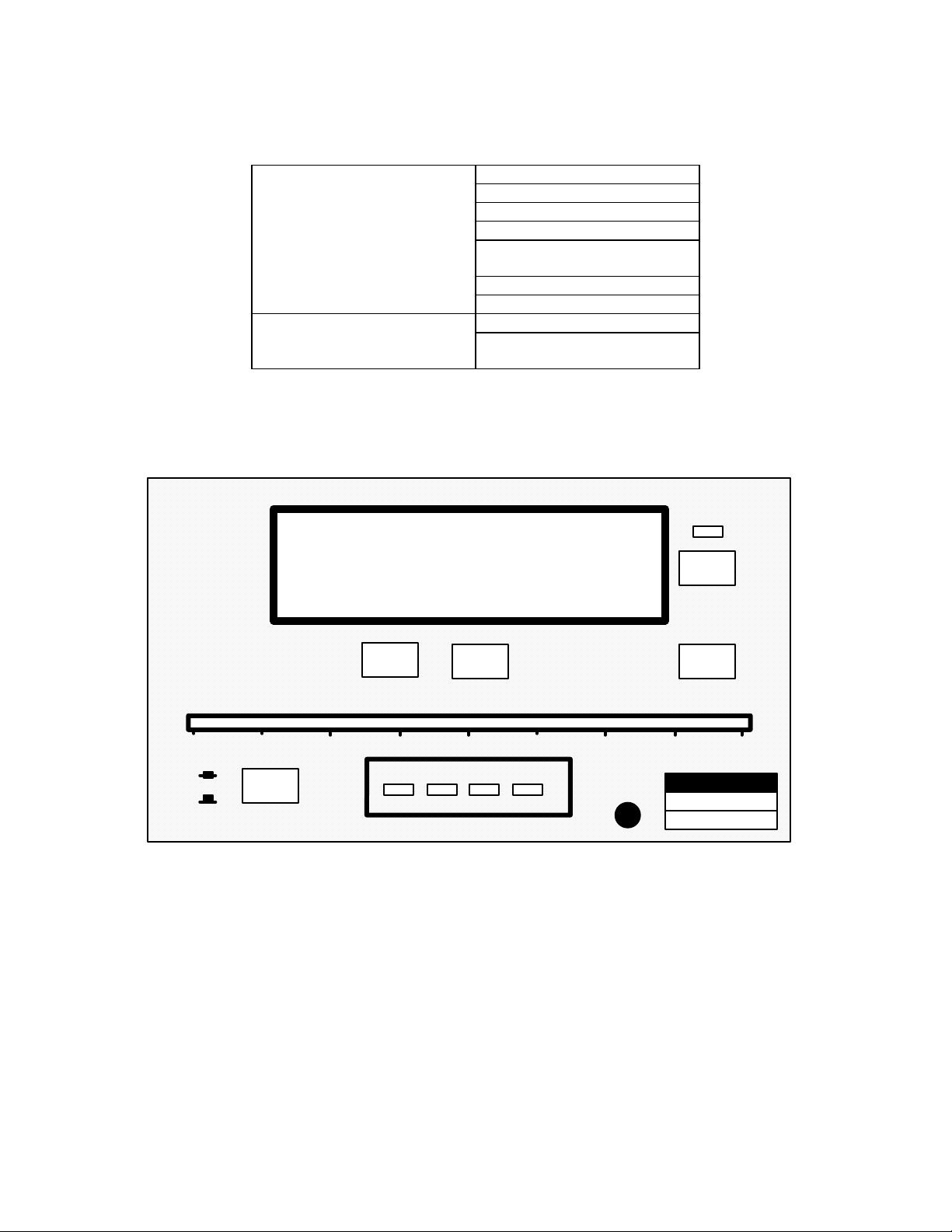
The UDR provides display, control, and annunciation functions for the monitoring system. Refer to Figure
1-2 for view of the 946A-200 front panel.
Standard features for the instrument consist of a three digit display of the radiation value and a multicolored bargraph indicator which covers the entire range of the detector. The bargraph will change color
in the event of an alarm condition. Front panel alarm indicators and rear panel output relays for alarm
annunciation are also included. Front panel pushbuttons are provided to apply power, display alarm limit
set points, for alarm acknowledgment, and the activation of a check source function.
Analog outputs of 0 to 10 VDC and 4 to 20 mA (2) are provided for recording and computer monitoring.
The 0 to 10 VDC output may also be used to drive a remote meter or a local (i.e. near the detector)
indicator.
All electronics required to interface to the VICTOREEN 977-210 series detector/preamplifier are included
within the 946A-200 UDR. These electronics consist of a low voltage power supply, and the
hardware/software required for UDR operation. The system also includes a positive overrange indication
on the display when radiation intensity exceeds the full scale value of 10
7
mR/h.
The following paragraphs describe the available options. A separate manual, for each option board, is
available with more detailed information. Listed below are the option boards currently available.
1. 942-200-75: ANALOG OPTION INPUT BOARD - (Generally not used for normal operation with the 946A-200
UDR, however, it is used if the UDR is part of a simulator) Contains four separate channels for analog input. A 0
to 10 VDC input or 4 to 20 mA input can be selected independently for each channel using the jumpers and
switches provided on the board. Possible inputs to the board include: temperature, pressure, flow, or simulated
radiation.
2. 942-200-80: COMMUNICATIONS LOOP OPTION BOARD - Designed to enable a EIA RS232C serial
communications link between VICTOREEN's ratemeter and a user computer system or CRT terminal, with baud
rates ranging from 50 baud to 19200 baud. An asynchronous communication interface adapter is utilized to
format the data and control the interface.
The Communication Loop Option Board also provides an isolated multi-drop, serial communications port for
interface with a supervisory computer system. The serial data is in a modified RS232 format, and utilizes
Victoreen’s proprietary VICO loop protocol. For maximum electrical noise protection, a six conductor
communication cable is used.
The 946A-200 UDR has one standard 942-200-80 Communications Board to support communications between
the preamplifier and the 977-210 Detector/Preamplifier.
3. 942-200-95: ANALOG OUTPUT BOARD - Designed to provide a user selectable single output voltage of: 0 - 10
Vdc, 0 - 5 Vdc, 0 - 1 Vdc, 0 - 500 mVdc, 0 - 100 mVdc, 0 - 50 mVdc, or 0 - 10 mVdc.
4. 942-200-95M1: DUAL ANALOG OUTPUT BOARD - Designed to provide two user selectable output voltages.
Output #1 is either 0 - 5 Vdc, or 0 - 10 Vdc, while output #2 is either 0 - 10 mV dc, 0 - 50 mVdc, 0 - 100 mVdc, 0 500 mVdc, or 0 - 1 Vdc.
1-4
Page 13
Application
The Model 946A-200 UDR may be used with all VICTOREEN 977 series Ion Chamber Detectors. The
detector/preamplifier, when connected to the UDR, will comprise a single channel digital area monitoring
system. For additional information on various applications, please contact VICTOREEN, Inc.,
Applications Engineering Group.
Specifications
General specifications for the 946A-200 UDR are listed below. The 946A-200 is rated for nuclear
applications, and
any repairs to it by personnel not qualified to ANSI 45.2.6, 1978, Skill Level II will void
the nuclear rating.
Main Display
Bargraph Display
(Dynamic Range)
Alarm Indicators
Alarm Delay
Display Selection
(Momentary Pushbuttons)
Check Source
Alarm Ack.
Power ON/OFF
Relay Outputs
(Failsafe operation)
Analog Outputs
Alarm Ack Input
UDR Electronic Accuracy
Dimensions
(H x W x D)
Weight
Power
Operating Temperature
Relative Humidity
Compatible Detector
Three digits with backlighted radiation units display and floating
decimal point. Three digits plus exponent for data entry/display
Three segments per decade, 10-1 to 107 mR/h (24 segments), tricolor, indicating channel status.
HIGH Alarm (Red LED) - Flashing until acknowledged
WARN Alarm (Amber LED) - Flashing until acknowledged
FAIL Alarm (Red LED) - Does not flash, is not manually acknowledged
RANGE Alarm (Red LED), overrange/underrange - Does not flash,
automatically acknowledges
3 minute alarm mute on channel power-up
HIGH, High Alarm limit
WARN, Warn Alarm limit
Activates electronic Check Source and associated green LED
indicator. “Latching pushbutton operation”
Alarm acknowledgment: causes alarm indicators to go to a steady on
state after acknowledgment, relays will reset when radiation level
drops below setpoint. Internal jumper causes alarms to be reset
automatically when radiation level drops below set point (no operator
input required).
Alternate action push-button for AC power to the unit
HIGH Alarm - 1 set. DPDT rated 5 A @ 120 Vac (one set 120 Vac
powered for use with optional local alarm)
WARN Alarm - 2 sets. DPDT rated 5 A @ 120 Vac
FAIL Alarm - 2 sets. DPDT rated 5 A @ 120 Vac
DC contact rating for all relays is 5 A @ 29 VDC
4 to 20 mA (2) and 0 to 10 Vdc, logarithmic and may be scaled for any
one decade (minimum) to the full range of the unit (maximum)
Optically isolated DC input
± 1% digit (± 1% of the displayed value), exclusive of the detector
energy response
3.5 in. x 5.6 in. x 13.5 in.
(8.9 cm x 14.2 cm x 34.3 cm)
Approximately 3.7 lb. (1.67 kg)
120 Vac ±10%, 50/60 Hz, 28 watts (240 Vac optional)
32° F to 122° F ( 0° C to + 50° C )
0 to 95% non-condensing
977 Series, Ion Chamber
1-5
Page 14
Auxiliary Equipment
Support/Test Equipment Model 848-8: Field Calibrator
Model 942TS: UDR Test Set
Model 948-1: Rack Chassis
Model 948A-4: Remote Alarm
Model 948-3: Table Top
Enclosure
Model 948-10: Panel Adapter
Model 50-150: Cable
Remote Indicator Model 948A-4: Remote Alarm
Model 948A-5: Remote
Alarm/Meter
kR/h
00.NNN
mR/h
R/h
CHECK
SOURCE
HIGH WARN
ON
1.1
OFF
Figure 1-2. Front Panel, Model 946A-200 Universal Digital Ratemeter
10 10 10 10 10 10 10
23 45 67
ALARMS
HIGH WARN FAIL RANGE
ALARM
ACK.
mR/h
MODEL 946A
VICTOREEN
1-6
Page 15

(BLANK PAGE)
1-7
Page 16

Page 17

Section 2 - Receiving Inspection and Storage
Receiving Inspection
Upon receipt of the unit:
1. Inspect the carton(s) and contents for damage. If damage is evident, file a claim with the carrier and
notify the Victoreen Customer Service Department.
Fluke Biomedical RMS
6045 Cochran Rd.
Cleveland. Ohio 44139
Phone: (440) 248-9300
Fax: (440) 349-2307
2. Remove the contents from the packing material.
3. Verify that all items listed on the packing list have been received and are in good condition.
NOTE
If any of the listed items are missing or damaged, notify the Fluke
Biomedical RMS Customer Service Department.
Storage
Storage of Fluke Biomedical RMS instruments must comply with Level B storage requirements as
outlined in ANSI N45.2.2 (1972) Section 6.1.2(.2). The storage area shall comply with ANSI N45.2.2
(1972) Section 6.2 Storage Area, Paragraphs 6.2.1 through 6.2.5. Housekeeping shall conform to ANSI
N45.2.3 (1972).
Level B components shall be stored within a fire resistant, tear resistant, weather tight enclosure, in a well
ventilated building or equivalent.
Storage of Fluke Biomedical RMS instruments must comply with the following:
1. Inspection and examination of items in storage must be in accordance with ANSI N45.2.2 (1972)
Section 6.4.1.
2. Requirements for proper storage must be documented and written procedures or instructions
must be established.
3. In the event of fire, post-fire evaluation must be in accordance with ANSI N45.2.2 (1972),Section
6.4.3.
4. Removal of items from storage must be in accordance with ANSI N45.2.2 (1972), Sections 6.5
and 6.6.
2-1
Page 18

(BLANK PAGE)
2-2
Page 19

Installation
Section 3 - Installation
Installation consists of mounting the equipment, making the required electrical connections, and entering
the desired set points. Installation drawings are provided in Appendix B of this manual.
CAUTION
Remove all power prior to installing the UDR.
Detector Mounting
Refer to Engineering Drawing GEL 977-210, provided in Appendix B, for detector and preamplifier
mounting dimensions, weights and recommended fasteners.
UDR Mounting
The UDR is a self contained unit which can be mounted in four different ways.
CAUTION
When installing the UDR in enclosed panels or cabinets, ensure that the maximum
operating temperature (122° F) is not exceeded. The total heat load should be
calculated to determine whether cooling by natural convection or forced
ventilation (i.e. fans) is required. The heat load for a single UDR is approximately
96 BTU/hr.
When more than four units are to be mounted in a cabinet, it is recommended that
the center position in each chassis be left blank to facilitate the flow of cooling air
through the cabinet.
NOTE
For seismic applications, the rear of the chassis must be supported, or the sides of
the chassis must be fastened together. For further information, contact Fluke
Biomedical RMS.
1. The first mounting utilizes a 19 inch rack chassis adapter, Victoreen Model 948-1. This configuration
requires 3.5 inches of rack height and can be used to mount up to three UDRs side by side. A blank
filler panel, Victoreen Model 948-2, is available to cover unused mounting positions. In multiple UDR
installations, the center mounting bay should be fitted with a Model 948-2 blank panel to facilitate
cooling air flow.
2. The second mounting consists of a single channel table top enclosure, Victoreen Model 948-3.
Dimensions for the enclosure are 4.5 inches high by 6.8 inches wide by 14.9 inches deep. This
enclosure is used primarily in a laboratory environment. Refer to drawing 948-3-5 for mounting
dimensions.
3. The third mounting consists of a panel mount enclosure, Victoreen Model 948-9. Cutout dimensions
for this enclosure are 3.75 inches high by 6.45 inches wide, the outside dimensions for the enclosure
are 4.0 inches high by 6.7 inches wide by 13.7 inches deep. This mounting must also be rear
supported in seismic applications. Refer to drawing 948-9-5 for mounting dimensions.
3-1
Page 20

4. The fourth mounting utilizes the Victoreen Model 948-10 Rack Chassis Adapter to mount a 946A-200
UDR into an existing Victoreen analog meter rack chassis, such as those used for the Victoreen 842
series of analog ratemeter.
The UDR is simply inserted into the selected mounting enclosure and secured using the front panel pawl
fastener.
WARNING
Ensure all power is off prior to connecting the field wiring.
Electrical Interface
Electrical connections at the preamplifier are made via the mating “MS” style connector supplied with the
detector. It is not necessary to open the preamplifier enclosure to complete the interconnection to the
ratemeter. The desiccant bags inside the preamplifier enclosure should be checked for moisture
absorbtion prior to placing into service. Each bag contains a color indicator that indicates when it should
be replaced.
NOTE
The electrometer circuitry in the preamplifier is highly sensitive to moisture and
physical damage. Use extreme care when the preamplifier case is opened as the
high impedance electrometer circuitry is easily damaged. Do not leave the
preamplifier enclosure in the open position for any extended period of time.
Electrical interconnections at the Model 946A-200 Readout are performed using the mating connector kit,
VICTOREEN part number 946A-100-4 (supplied with the Readout), by using the connector Input/Output
assignments provided in Tables 3-1 through 3-6, and the drawings provided in Appendix B. Refer to
drawing 945A-3, showing complete channel loop wiring, including remote alarms (if used)
Connector pins should be soldered to customer furnished cable, using 60/40 tin/lead resin core solder
with a soldering iron of 50 watts or less to avoid connector damage.
Table 3-1. Rear Panel Connections
Connector Contact Function
P1 Relay, Remote Alarm
Acknowledge
P2 Detector Connector, VICO
Loop Communications,
Remote Alarm Output
P3 AC Power Input
P6 Analog Outputs (4 - 20 mA, 0 -
10V)
P7 RS232C Communications
3-2
Page 21

Table 3-2. Connector P1 - Input/Output
Pin Signal Internal Connection
1 Spare Not Used
2 Spare Not Used
3 Spare Not Used
4 Spare Not Used
5 Spare Not Used
6 Spare Not Used
7 Fail Relay, common Relay Board K3-A
8 Fail Relay, n.o. Relay Board K3-B
9 Fail Relay, n.c. Relay Board K3-C
10 Fail Relay, common Relay Board K3-D
11 Fail Relay, n.o. Relay Board K3-F
12 Fail Relay, n.c. Relay Board K3-E
13 Warn Relay, common Relay Board K4-A
14 Warn Relay, n.o. Relay Board K4-B
15 Warn Relay, n.c. Relay Board K4-C
16 Warn Relay, common Relay Board K4-D
17 Warn Relay, n.o. Relay Board K4-F
18 Warn Relay, n.c. Relay Board K4-E
19 Alarm Relay, common Relay Board K5-A
20 Alarm Relay, n.o. Relay Board K5-B
21 Alarm Relay, n.c. Relay Board K5-C
22 Spare Not Used
23 Spare Not Used
24 Spare Not Used
25 + Remote Acknowledge Main Circuit Board J9-1
26 - Remote Acknowledge Main Circuit Board J9-2
27 Spare Not Used
28 Spare Not Used
29 Spare Not Used
30 Spare Not Used
31 Spare Not Used
32 Spare Not Used
33 Spare Not Used
34 Spare Not Used
35 Spare Not Used
36 Spare Not Used
37 Spare Not Used
n.o. = normally open
n.c. = normally closed
Relay contacts listed are in the shelf or de-energized state. Relays are operated in the fail-safe mode,
de-energizing to indicate a tripped condition.
3-3
Page 22

Table 3-3. Connector P2 - Detector Connector
Pin Signal Internal Connection
1 +15 VDC Not used in most applications
2 -15 VDC Not used in most applications
3 Supply Ground Power Supply Ground
4 Transmit + Communication Board
5 Transmit - Communication Board
6 Receive + Communication Board
7 Receive - Communication Board
8 Loop Voltage +
Communication Board
Fused + 15 VDC
9 Loop Voltage -
Communication Board
Fused -15 VDC
10 0 - 10 Vdc* Main Circuit Board J5-10
11 Ground Main Circuit Board J5-9
12 Check Source Line Not used in most applications
13 Neutral Not used in most applications
14 Alarm Switched Line Not used in most applications
* 0 - 10 Vdc selected for customer use on P2 (10,11) or P6 (5, 6), not both.
Table 3-4. Connector P3 - Power Input
Pin Signal Internal Connection
1 120 Vac, Line Line fuse (F2)
2 120 Vac, Neutral Power Supply, 120 Vac (n)
3 Safety Ground Chassis
3-4
Page 23

Table 3-5. Connector P6 - Auxiliary I/O
Pin Signal
1 4 - 20 mA Output # 1
2 Ground
3 4 - 20 mA Output # 2
4 Ground
5 0 - 10 V *
6 Ground
7 Analog Output Option
8 Ground
17 Not Used
18 Not Used
19 Not Used
20 Not Used
21 Not Used
22 Not Used
23 Not Used
24 Not Used
* 0 - 10 Vdc selected for customer use on P2 (10,11) or P6 (5, 6), not both.
Table 3-6. Connector P7 - RS232C
Pin Signal
1 Protective Ground
2 Transmit Data
3 Receive Data
4 Request to Send (RTS)
5 Clear to Send (CTS)
6 Data Set Ready (DSR)
7 Signal Ground
8 Receive Line Signal Detect
20 Data Terminal Ready
3-5
Page 24

Set-up
To place the UDR in operation, the following steps should be performed:
NOTE
Ensure you have read and fully understand section 4, prior to continuing.
1. Verify jumpers and DIP switches on the preamplifier and ratemeter are set for the operational
features desired. Refer to Section 4 Tables 4-3 through 4-6 for additional information.
2. Apply power to the unit.
3. Enter detector dependent set points such as analog output, High/Low scale Value, and calibration
constant, using the procedure outlined in Section 4, and Tables 4-2 & 4-7.
4. Enter channel dependent setpoints such as Alarm Limits are to be entered using the procedure
described in Section 4, and Tables 4-2 & 4-7.
5. Electronic adjustments affecting calibration are factory set and should not be readjusted for initial
operation unless the UDR has been in storage for more than one year. If the Unit has been in
storage for more than one year, the electronic calibration described in Chapter 6 should be
performed.
3-6
Page 25

Section 4 - Operation/Functional Description
Operation
This section describes the operation and set up of an area monitoring system consisting of a Model
946A-200 UDR and a Model 977-210 Detector/Preamplifier interconnected via a serial communications
interface. The detector preamplifier provides the electronics interface between the detector and the UDR.
It consists of a high voltage/communications interface printed circuit board and an electrometer printed
circuit board. The preamplifier measures the current output of the ion chamber, generates the high
voltage supply for the detector, performs periodic diagnostic checks, and performs an electronic check
source function on demand from the UDR. The current measurement is converted to a dose rate and
this, along with the operational status of the preamplifier and detector, are transmitted to the UDR.
The 946A-200 UDR uses this information to generate the dose rate display, error codes, alarms, and
analog outputs.
Operation of the 946A-200 UDR consists of operator functions and configuration functions. All operator
functions are performed using the front panel shown in Figure 4-1. Configuration functions are performed
using internal switches and/or jumpers, which are accessible with a partial removal of the UDR from the
mounting enclosure (refer to Table 4-6). Calibration involving trimpots are described in Section 6.
Detector Operation
The Model 977-210 wide range ion chamber detector is an eight decade, linear reading radiation monitor.
The chamber, cables, and preamplifier are sensitive to moisture; therefore, the detector and preamplifier
are sealed. The preamplifier box contains a desiccant package to remove moisture from the interior of
the preamplifier. The desiccant has a color indicator to show when it should be replaced.
The detector electrometer converts the current from the ion chamber to a voltage which is measured by
the analog to digital converter of the preamplifier. Under program control, this measurement is made
every 50 milliseconds on the first five decades and every 100 milliseconds on the upper three decades.
The electrometer is auto-ranging and auto-zeroing. An internal coarse zero control (factory adjusted) is
provided. The microprocessor in the preamplifier performs data collection, averaging, multiplication by a
stored calibration factor, range changing, high voltage check, detector cable integrity check, and
communication with the 946A-200 UDR.
The high voltage check and integrity check are run, under program control, every 256 seconds. The high
voltage check is a measurement of the high voltage to ensure that the value is sufficient for 100%
collection at full scale.
4-1
Page 26
The detector cable integrity check is a pulse that is injected on the detector high voltage. The chamber
capacitance couples the pulse into the electrometer where it is seen as a high current. If either the high
voltage lead or signal lead are not connected to the chamber, the pulse does not appear on the
electrometer. The measurement cycle is interrupted for approximately one (1) second whenever the
integrity check is performed. The integrity check and high voltage check are not performed when the
instrument is reading on the three highest decades. A reading in these ranges serves as an indication of
the functioning of the instrument. The Maintenance mode operation also inhibits these checks from being
made.
There is a hysteresis built into the range changing function of the electrometer. The range change-up
occurs at the decade points whereas the range change-down occurs at 80% of the decade points. This
hysteresis results in the display of only two significant digits when in the upper 20% of a decade.
Whether or not this occurs depends on which direction the radiation level is trending. An increasing trend
will result in three significant digits while a decreasing trend will result in two significant digits.
The response times for a change in reading within the same decade are listed in Table 4-1. If a change
of 100 to 1000 times the current reading occurs, the instrument will range change within a single 50
millisecond clock cycle.
Table 4-1. Response Time
DECADE RANGE RESPONSE TIME
1 0.1 to 1.0 mR/h 80 sec.
2 1.0 to 10 mR/h 32 sec.
3 10 to 100 mR/h 16 sec.
4 100 to 1000 mR/h 4 sec.
5 1.0 to 10 R/h 2 sec.
6 10 to 100 R/h 0.9 sec.
7 100 to 1000 R/h 0.2 sec.
8 1.0 k to 10 kR/h 0.2 sec.
A manual electronic check source may also be initiated from the UDR by the operator to check detector
operation. Upon removing the check source request, the UDR again displays the detector output
CAUTION
Do not actuate the check source when the reading is above 1 R/h.
The radiation measurement is additive to the check source signal
resulting in improper values from the check source. This may
result in the UDR indicating a failure when the instrument is
operating correctly.
The detector preamplifier contains a High Voltage/Communications Interface Board containing an RS232
driver, a Victoreen Communications Interface Driver, the detector high voltage power supply, a local 0 10 Vdc analog output, and a -12 Vdc open collector alarm output.
4-2
Page 27

Operation / Functions
Operation of the 946A-200 UDR consists of operator functions and configuration functions. All operator
functions are performed using the front panel. Configuration functions are performed using internal
switches and/or jumpers which are accessible with a partial removal of the UDR from the mounting
enclosure.
Normal Operation
If the measured radiation field is within the range of the detector during power-up, the mR/h, R/h, or kR/h
value will be displayed as a three digit number with a floating decimal point (i.e. .XXX mR/h). The
bargraph will display the value of radiation, with a resolution of three segments per decade, over the
range of the detector or eight decades. The bargraph should be green, providing the operator with a
visual indication of normal operation. All other indicator LEDs should be off. In very low background
environments (< 0.1 mR/h), the range indicator LED may be illuminated.
WARN/HIGH Alarms
If the measured radiation field increases above the WARN alarm limit, the WARN alarm indicator will turn
on flashing (amber color), the bargraph will change color to amber, and the warn alarm relay will deactivate. If the measured radiation field increases above the HIGH alarm limit, the HIGH alarm indicator
will turn on flashing (red color), the bargraph will change color to red, and the high alarm relay will deactivate.
NOTE
Non-failsafe relay operation for the HIGH and WARN alarms is available as an option at time of purchase.
The UDR can be configured to automatically reset the alarm relays and alarm indicators by removing
JP3-3, or it can hold the alarm relays energized and flash the alarm indicators until the alarm
acknowledge (ALARM ACK) push-button is pressed. If the ALARM ACK push-button is pressed while the
alarm condition still exists, the indicators will go to a steady state, and the relays will remain energized
until the alarm condition returns to normal. Upon resumption of normal operation, the relays and alarm
indicators will de-energize. The bargraph color will always indicate the current status; green for normal,
amber for warn, and red for a high alarm.
Front panel pushbuttons labeled HIGH and WARN can be used to display the respective alarm set points.
Range Alarm
If the measured radiation field is below the Underrange setpoint, the front panel display will indicate 0.00
mR/h, and the RANGE alarm indicator will illuminate in red, the bargraph will indicate the actual radiation
value, and the analog output will be set to zero. The minimum range is an adjustable setpoint and is
defaulted to 1.00-1 mR/h. When the measured radiation field increases into the range of the detector, the
RANGE alarm indicator will extinguish and normal operation will continue.
If the measured radiation field goes above the overrange set point, the RANGE alarm indicator will
illuminate and the front panel display will indicate EEEEE, the bargraph will illuminated in RED, and the
analog output will be set to full scale. The maximum range of the detector is used is determine by the
overrange set point. When the measured radiation field returns within the maximum operating range of
the detector and the condition is acknowledged, the RANGE alarm indicator will extinguish and normal
operation will resume.
4-3
Page 28

Fail Alarm
Detector failure, communication loss, or UDR microprocessor failure are some of the conditions which
can produce a FAIL alarm and in some cases an error display. The fail condition is true whenever an
equipment failure is detected and false when no equipment failures are detected. When a fail condition
occurs, other than power failure, the red FAIL alarm indicator illuminates and the fail relay coil deenergizes.
A FAIL alarm will clear automatically when the failure conditions are no longer present.
Check Source
The check source push-button and electronics are provided to verify detector operation. To operate the
check source, press the CHECK SOURCE push-button and hold it down for one second. The electronic
check source circuit will energize, the check source indicator will illuminate (green), and the check source
radiation value will be displayed on the front panel. Pressing the CHECK SOURCE push-button again will
cause the UDR to return to normal operation. Removing JP3-5 allows alarms to be activated if alarm
limits are exceeded by the check source radiation value. Installing JP3-5 allows alarms to be muted if
alarm limits are exceeded by the check source radiation value.
The analog outputs are set to zero during check source operation.
A built-in timer will turn the Check Source OFF after 10 minutes.
Firmware Version
Both detectors and UDR require a programmed PROM for operation. For the part number and the latest
revision of these PROMs, see the detector Calibration Data Sheet and/or Factory Test Data Sheet.
4-4
Page 29

Operational Modes
Rate Mode (Normal Operation)
The system is in RATE MODE when SW3-3 on the high voltage /comm board (Model 977-210-10) in the
preamplifier is set to the OFF position, the UDR function switch is in any position, but 8 or 9, and the
Check Source button is OFF. In the Rate Mode, the display shows the dose rate data received from the
preamplifier in mR/h, R/h, or kR/h units as appropriate. The bargraph also shows the dose rate. The
color of the illuminated segments is green when the dose rate is below the WARN setpoint, amber when
the dose rate is above the WARN setpoint and below the HIGH setpoint, and red when the dose rate is
above the HIGH setpoint. The analog outputs are active while the UDR is in RATE MODE and all alarms
are enabled.
Data Entry Mode
Data Entry Mode is selected by pressing the ENTER push-button while the rotary FUNCTION switch is in
a valid setpoint position (see How to Enter Setpoints). The selected setpoint is displayed in exponential
format (e.g. 1.00E2) with the left most digit flashing. If the FUNCTION switch is not in a setpoint position,
pressing the ENTER button has no effect. Refer to Table 4-2 for FUNCTION switch positions.
In the Data Entry Mode, the alarms, bargraph and analog outputs are active. The check source and
alarm acknowledge functions are inoperative.
Alarm Inhibit Mode
Alarms are inhibited in situations where an alarm trip would be meaningless, because the UDR
preamplifier is not in a normal measurement mode (i.e., when the UDR is in the Check Source Mode).
New alarm trips cannot occur and old alarms cannot be reset. When the inhibit period is over, alarm trips
and resets are enabled again. Alarm inhibit conditions are discussed in the following paragraphs. Alarms
are inhibited for three minutes after channel power-up to allow time for induced charges within the
detector output to subside.
Check Source Mode
In the Check Source Mode, the dose reading displayed is the result of pulsing the high voltage to the
detector to simulate a radiation field. The value displayed is in the nominal range of 2.5 to 5 R/h and is
dependent on component value and gain in the check source driver. When in the check source mode,
alarms may be inhibited or active depending on jumper selection (JP3-5). Analog outputs are always set
to zero during check source operation.
To operate the check source, press the CHECK SOURCE push-button and hold it down for
approximately 1 second. The electronic check source circuit will energize, the green check source
indicator will illuminate (approximately 1 second after the button is depressed), and the check source
radiation value will be displayed on the front panel. An internal configuration jumper allows alarms to be
activated or muted if alarm limits are exceeded by the check source radiation value. The alarm inhibit
function may be disabled by removing jumper JP3-5 from the UDR main board. If this is done, alarms will
be enabled in Check Source Mode.
Pressing the CHECK SOURCE push-button again will cause the UDR to return to normal operation.
A built-in timer will turn the Check Source OFF after 10 minutes.
4-5
Page 30

CAUTION
Do not actuate the check source when the reading is above 1 R/h.
The radiation measurement is additive to the check source signal
resulting in improper values from the check source. This may
result in the UDR indicating a failure when the instrument is
operating correctly.
NOTE
The Check Source relay, though energized in the Check Source
Mode, Does not have an active function in the 945A Area Monitoring
System.
The bargraph operates normally during Check Source operation.
The analog outputs are set to zero ( i.e. 0 Vdc or 4 mA) during Check Source operation.
Maintenance Mode
The Maintenance Mode is designed to allow adjustments to be made on the electrometer board in the
preamplifier without tripping the FAIL alarm. Maintenance Mode is selected by setting SW3-3 on the 977
interface board, in the preamplifier, to the ON position.
The bargraph works the same as in Rate Mode. The units on the numeric digital display flash as long as
data is being received from the preamplifier. If communication with the preamplifier fails, the flashing
stops.
The FAIL alarm and all failure error codes except E0007 (communications failure) are inhibited. The
UDR analog outputs are active. The local preamplifier analog output may be checked at this time. SW34 in the OFF position forces the output to zero; SW3-4 in the ON position forces the output to full (refer to
Table
4-3).
The HIGH, WARN, and RANGE alarms may be inhibited during Maintenance Mode by setting SW3-2 on
the 977 interface board to the OFF position. These alarms are enabled when SW3-2 is in the ON
position.
4-6
Page 31

Auto Zero Mode
The contents of the auto zero counter, in the preamplifier, may be displayed at any time by placing the
UDR function switch to position 8. The display shows the current value of the counter and is updated
about once per second.
All units flash once per second as long as data is being received from the preamplifier. If a
communications break occurs, the units will stop flashing.
All alarms and error codes are inhibited except E0007 (loop fail).
The bargraph is blanked and the analog outputs are at low scale while the auto zero counter is displayed.
Refer to "Auto Zero Failure" and "Auto Zero Set-Up" for more information on the Auto Zero Mode.
Loop Test Mode
The functioning of the preamplifier communications loop can be tested by looping +TX and -TX back to
+RX and -RX on the UDR P2 connector and setting the UDR FUNCTION switch to position 9. While
executing the loop test, the bargraph will light (green) from left to right as characters are sent. The
numeric display will be blanked. If the test fails, the display will show E0009 and the bargraph will be red.
This test verifies proper operation of the UDR transmit/receive function, and may be used to determine if
the source of a communications error is in the UDR or the preamplifier.
The test runs continuously until the UDR FUNCTION switch is moved out of position 9.
All alarms are inhibited and the analog outputs are at low scale while the loop test is running.
There is an available device as part of the 942 Test Set for use with loop tests (P/N 942TS-100-45) that is
plugged into P2 to perform the interconnection function.
Alarms
The alarm functions provided by the UDR include HIGH, WARN, FAIL, and RANGE. The HIGH, WARN ,
and FAIL alarms drive relay contact outputs. Some operating modes of the UDR disable alarms. The
user is cautioned to read and fully understand section 4.
Alarm Logic
Alarm logic defines whether alarm relay coils are energized or de-energized in normal operation.
Standard alarm reset logic for the UDR is manual reset for the HIGH, and WARN alarms, and auto reset
for the FAIL and RANGE alarm.
Auto reset for HIGH and WARN alarms may be selected by jumper JP3-3.
4-7
Page 32

Manual Reset
When an alarm trips, the relay coil goes to its abnormal position. The indicator flashes until the alarm is
acknowledged by pressing the ALARM ACK button on the UDR. The indicator then remains steady on
until the alarm condition becomes false. At that time, the alarm resets by turning the indicator off and
returning the contact to its normal position.
Auto Reset
When an alarm trips, the contact goes to its abnormal position. The indicator goes steady on. When the
alarm condition becomes false, the alarm automatically resets, returns the relay coil to normal position,
and turns the indicator off.
Auto reset may be selected for the HIGH and WARN alarms by removing jumper JP3-3 from the UDR
main board.
Standard relay operation for the UDR is fail-safe. When the unit is powered, the relay coil energizes. If
power is lost to the relay coil, or an alarm condition occurs, the relay de-energizes, giving a trip indication.
This logic provides fail-safe operation for the alarm function.
Non-fail safe relay operation for the HIGH and WARN alarms is available as an option.
HIGH Alarm
The HIGH alarm condition is "true" when the display dose rate is greater than or equal to the HIGH alarm
set point and "false" for all other conditions.
The standard logic for the HIGH alarm is fail-safe, manual reset.
When the HIGH alarm is tripped, the red HIGH alarm indicator begins flashing, the bargraph goes to red,
the HIGH alarm relay coil de-energizes, and the UDR commands the preamplifier to set its auxiliary
output high. When the alarm is acknowledged, the HIGH alarm indicator goes steady on and the UDR
commands the preamplifier to set its auxiliary output low. The auxiliary output on the preamplifier can be
used to drive a remote alarm/alarm indicator. The HIGH alarm relay will change state when the radiation
value drops below the setpoint if the alarm has been acknowledge.
The HIGH alarm is inhibited in Auto-Zero and Loop Test modes, and may be inhibited in Check Source
and Maintenance modes via jumper selection.
WARN Alarm
The WARN alarm condition is "true" when the display dose rate is greater than or equal to the WARN
alarm set point and "false" for all other conditions.
The standard logic for the WARN alarm is fail-safe, manual reset.
When the WARN alarm is tripped, the amber WARN alarm indicator begins flashing, the bargraph goes to
amber, the WARN alarm relay coil de-energizes. When the alarm is acknowledged, the WARN alarm
indicator goes steady on. With the alarm acknowledged, the relay will change state when the radiation
value drops below the setpoint.
The WARN alarm is inhibited in Auto-Zero and Loop Test modes, and may be inhibited in Check Source
and Maintenance modes via jumper selection.
4-8
Page 33

RANGE Alarm
The underrange condition is "true" when the dose rate is below the underrange setpoint and "false" for all
other conditions. The RANGE indicator illuminates, the analog output is set to zero, and the display
reads 0.00 mR/h when the underrange condition is true. The bargraph will operate normally.
The underrange condition clears automatically when the detector output returns within the normal range.
There is no relay contact associated with the underrange alarm.
The overrange is true when the dose rate is greater than or equal to the overrange set point or the
preamplifier is sending an overrange status to the UDR. The condition is false when neither of the above
conditions is true.
When the OVER RANGE alarm is active; WARN and HIGH alarms are true, the red RANGE indicator
illuminates, the bargraph illuminates red, the analog output reads full scale, and the display reads
EEEEE. The default overrange setpoint is 1.00E7 mR/h.
Once the radiation value is less than the setpoints, the overrange condition may be manually reset to
return to normal operation. There is no relay contact associated with the overrange alarm.
FAIL Alarms
Several equipment failure conditions are monitored which produce a FAIL alarm and in some cases an
error message. The fail condition is "true" whenever any equipment failure is detected and "false" when
no equipment failures are detected. When a fail condition occurs, other than power failure, the red FAIL
alarm indicator illuminates and the fail relay coil de-energizes.
The FAIL alarm logic is always fail-safe, auto reset.
The following are the fail alarms included in the 946A-200 UDR:
1. LOW SIGNAL Failure
2. AUTO ZERO Failure
3. HIGH VOLTAGE Failure
4. LOOP Failure (communications)
5. POWER Failure
6. MPU Failure (hardware) in either detector or UDR
Low Signal Failure
If the dose rate reported to the UDR by the preamplifier is zero for five minutes, a low signal failure is
detected. A low signal alarm usually indicates a failure in the electrometer since normal leakage currents
will result in a non-zero dose rate. The UDR display may read zero for five minutes or more without a low
signal fail alarm. In this case, the preamplifier is reporting a dose rate that is below the underrange
setpoint value. The low signal failure alarm can be disabled by removing jumper JP3-4 from the UDR
main board. Error code E0011 will be displayed under the fail conditions given.
4-9
Page 34

Auto Zero Failure
If the preamplifier zero offset correction is near its limit, the preamplifier notifies the UDR. Error code
E0012 is displayed. The zero offset correction is related to the value of the auto zero counter which can
be displayed by setting the FUNCTION switch to position 8. A value of 0 to 255 is possible. A value that
is significantly different from 128 indicates that an auto zero adjustment on the electrometer board, in the
preamplifier, is needed.
High Voltage Failure
The preamplifier checks the ion chamber integrity approximately every four (4) minutes by pulsing the
high voltage and checking the response. This operation has no effect on the dose rate reported to the
UDR. If the integrity test fails, the failure is reported to the UDR, and the UDR will display E0011.
This failure generally indicates a loss of continuity in the ion chamber or bad connections between the ion
chamber and the preamplifier (cable failure). This failure will also occur if the high voltage drops to a
level such that 100% collection at full scale cannot be achieved by the ion chamber. If the detector is
disconnected for the purpose of inputting a test signal into the electrometer, the high voltage failure will
be detected. To prevent an unwanted FAIL alarm, during testing, the Maintenance Mode previously
described should be used.
Loop Failure
If the UDR does not receive a valid message from the preamplifier in ten seconds, a loop failure is
detected and an E0007 code is displayed.
The loop failure can originate from bad seating of the serial communications board in the UDR, bad
connections in the preamplifier, bad connections at the P2 connector of the UDR, a baud rate mismatch
between the setting on the serial board and that in the preamplifier, an invalid address setting on the
serial board, or blown loop fuses.
The baud rate of the preamplifier can be set to 300 or 4800 baud. SW3-1 on the 977 interface board
selects 300 when in the OFF position and 4800 in the ON position. 4800 baud is the normal factory
setting. The address of the serial board must be set 4040. If the wiring of the serial option board to the
P2 connector is suspected, a loop test can be performed as described in "Loop Test Mode". The
instruction manual for the communications loop option board (P/N 942-200-80-1) contains details on how
to set up the serial board in the UDR.
Power Failure
If power is lost to the UDR, the bargraph, alarm indicators, and the display are blanked (turned off). The
HIGH, WARN, and FAIL relay coils de-energize.
MPU Failure
If the fail timer circuit, which monitors the MPU function, is allowed to time out (because of a hardware
failure), a failure condition will be true.
4-10
Page 35

Power Up Procedure
To place the system in operation, the following steps should be performed:
1. Verify that the UDR FUNCTION switch, located on the front right section of the UDR main board, is in
a position other than 8 or 9.
2. Verify that SW3-3 on the 977 interface board, located in the preamplifier enclosure, is set to the OFF
position.
3. Verify that the detector, preamplifier, and UDR are properly connected.
4. Apply power to the system. If all connections are good, the UDR will come up in the Rate Mode.
NOTE
The appearance of error codes E0002 or E0008 may indicate that the
setpoint memory has not been initialized. To initialize the set point
memory to the default values, power-up the UDR with the ENTER button
held down. (The UDR must be pulled out from its mounting to access the
ENTER button).
The appearance of error code E0007 indicates a communication failure.
Verify communication wiring, jumper and switch settings (refer to tables 43 and 4-5). Also check the communications board set-up using the
instruction manual provided in Appendix A.
When the system is first powered up, the preamplifier will detect a high
dose rate and pass this data to the UDR. This is the result of currents
generated by turning on the high voltage to the detector, and takes several
minutes to stabilize. The Overrange, High, and Warn alarms are inhibited
for three minutes after power-up. The analog outputs are at low scale
during this period.
5. Channel dependent set points, such as alarm limits, are to be entered using the procedure described
later in this section. The UDR contains default values for all setpoints to permit power-up prior to
user defined values being entered.
6. Electronic adjustments affecting calibration are factory set and should not be readjusted for initial
operation unless the UDR has been in storage for more than one (1) year. If the unit been in storage
for more than one (1) year, the electronic calibration described in section 5 should be performed.
How to Enter Setpoints
Available setpoints are listed in Table 4-2. The setpoints are accessed using the FUNCTION switch, the
DIGIT button, the VALUE button, and the ENTER button. These are located on the main printed circuit of
the UDR. The UDR must be pulled about halfway out of its rack chassis in order to access them. The
buttons are on the right side of the main board about two inches behind the front panel. The FUNCTION
switch is on the right side directly in front of the power supply.
4-11
Page 36

To display a setpoint, rotate the FUNCTION switch to one of the positions shown in Table 4-2 and press
the ENTER button. The setpoint will be displayed in exponential format with the leftmost digit flashing.
Pressing the ENTER button enters whatever is displayed into the non-volatile set point memory.
To change a setpoint, the DIGIT button is pressed and released until the digit to be changed is flashing.
Then the VALUE button is pressed and released until the desired value appears. This process is
repeated for all digits to be changed. The sign of the exponent can assume the values "E" or "-". The
former represents a positive power of 10 and the latter represents a negative power of 10.
When all digits and the exponent have been changed to their desired values, the ENTER button is
pushed to enter the new value into memory. Setpoint entries not accepted by the UDR are indicated by
the error code E0002 being displayed.
Table 4-2. Setpoints
Function Switch
Description Default Values Units
Position
0 HIGH Alarm Limit 1.00E5 mR/h
1 WARN Alarm Limit 1.00E3 mR/h
2 Overrange Limit 1.00E7 mR/h
3 Underrange Limit 1.00E-1 mR/h
4 Analog Full Scale 1.00E7 mR/h
5 Calibration Factor 1.00E2 percent
7 Analog Low Scale 1.00E-1 mR/h
Setpoint Descriptions
HIGH Alarm Limit
If the display dose rate is above the HIGH alarm limit, then the HIGH alarm is tripped. The HIGH alarm
limit must be greater than or equal to the WARN alarm and the underrange limit. It must be less than or
equal to the overrange limit.
WARN Alarm Limit
If the display dose rate is above the WARN alarm limit, then the WARN alarm is tripped. The WARN
alarm limit must be greater than or equal to the low scale value and less than or equal to the HIGH alarm
limit.
Overrange Limit
If the displayed dose rate goes above the overrange limit, the RANGE alarm is tripped. The overrange
limit must be greater than or equal to the HIGH, WARN, and Underrange setpoints.
4-12
Page 37

Underrange Limit
If the displayed dose rate goes below the underrange limit, an underrange condition is indicated. The
underrange limit must be less than or equal to the HIGH and WARN limits. Note the radiation display will
be 0.00 for dose rates under the underrange limit.
Analog Full Scale
This value is the dose rate at which the analog output is 10 volts or 20 milliampers. This value must be
an even power of 10 that is at least 1 decade higher than the low scale value. An even power of 10 is a
number of the form 1.00EX, where E indicates a positive exponent or “-” for a negative exponent any X is
an integer from -9 to +9.
Calibration Factor
The calibration factor is determined from the calibration data as the ratio of the theoretical to the actual
response of the detector. The permissible values are between 70% (7.00E1) and 129% (1.29E2). A
factor of 100% (1.00E2) gives no correction. The calibration factor is recorded on the calibration data
sheet supplied with the detector.
Analog Low Scale
This value is the dose rate at which the analog output is at 0 volts or 4 milliamperes. This value must be
an even power of 10 that is at least 1 decade less than the high scale analog output.
Set Point Error Codes
If, after entering a setpoint or upon power-up, an error code is displayed, it may be due to incorrect
setpoints. If error code E0002 or E0008 is displayed, all alarms are inhibited.
Code E0001 indicates that the display value is negative. This may indicate a defective EPROM or that
initialization of the unit is required. To initialize the setpoint memory to the default values, power up the
UDR with the ENTER button held down. After power has been applied, release and depress the ENTER
button and release again. If initializing the setpoint memory does not help, then the setpoint PROM is
defective or there is a hardware malfunction.
Code E0002 indicates that the combination of setpoints violates one or more of the rules stated under
setpoint descriptions. All setpoints should be checked for agreement with the setpoint descriptions.
The appearance of either code may indicate that the setpoint memory has not been initialized.
Code E0007 indicates a detector to preamplifier communications loop failure.
Code E0008 indicates that the analog output setpoints are invalid.
Code E0011 indicates a detector a high voltage power supply or cabling failure.
Code E0012 indicates an electrometer auto-zero adjustment is required.
Refer to Table 4-8 for a listing of all error codes.
4-13
Page 38

Analog Output
The analog outputs are a logarithmic function of the current UDR reading. The outputs are scaled by the
Full Scale Value and Low Scale Value, positions 4 and 7 respectively of the FUNCTION switch. An 8 bit
DAC is used to convert the displayed dose rate to a 4-20 mA or 0-10 Vdc output on connector P6 (on the
rear panel). Other outputs may be provided through the use of the Analog Output Option Board (942200-95). Refer to the option board manual for adjustment and value selection. The option board output
is also a logarithmic value. Output current or voltage is calculated using the following equations (shown
below):
P = log (R/LSV)/ [ log (FSV) - log (LSV) ]
and
V = P (VMax - VMin) + VMin or I = P (IMax - IMin) + IMin
where:
P = Percent of scale, expressed in a decimal number
R = Current reading
LSV = Low Scale Value
FSV = Full Scale Value
V = Voltage output
I = Current output
VMax = Maximum volt age available (usually 10 Vdc)
IMax = Maximum current available (usually 20 mA)
VMin = Minimum voltage available (usually 0 Vdc)
IMin = Minimum current available (usually 4 mA)
If the current reading (R) is greater than the full scale value (FSV) the output is limited to the MAX value (typically 10
Vdc or 20 mA).
As an example:
Assume: LSV = 1E-1, FSV = 1E7, R = 1E3, IMax = 20 mA, and IMin = 4 mA.
Then: P = [log (1E3/1E-1) ] / [ log (1E7) - log (1E-1)]
= log (1E4) / log (1E8)
= 4/8 = 0.5
and: I = 0.5 (20 mA - 4 mA) + 4 mA
= 0.5 (16 mA) + 4 mA
= 12 mA
To aid in calibrating the analog output, the high scale or low scale setpoint may be set to zero to force the
output high or low. If the low scale setpoint is set to zero, the analog output goes to low scale. If the high
scale value is set to zero, the analog output goes to full scale. If both are set to zero, the output goes to
full scale. Error code E0008 will be displayed if either setpoint is set to zero. The procedure for
calibrating the analog outputs is contained in Section 5.
4-14
Page 39

Victoreen Communications Loop
Communication between the detector preamplifier and the UDR is performed via a Victoreen loop, a
serial asynchronous communications interface. The communication utilizes Victoreen protocol and is
intended for use in electrically hostile environments where high noise immunity is required. Noise
immunity is achieved using differential line driving, and electrically isolating the end of each
transmit/receive pair with opto-isolators. Using a ±15 Vdc communications power supply, each 0 to 1
transition is equivalent to a 30 volt swing in loop voltage. Refer to the Model 942-200-80-1
Communications Board instruction manual located in Appendix A for further information.
Preamplifier Switch & Jumper Settings
Switch and jumper settings for the preamplifier are summarized in Table 4-3, 4-4, and 4-5.
Switch Normal Op. Switch Function
SW3-1 ON 0/OFF Selects 300 baud • 1/ON Selects 4800 baud (normal setting)
SW3-2 OFF 0/OFF Selects alarm inhibit, SW3-3 must be on for this state to be true.
SW3-3 OFF 0/OFF Selects Rate Mode (normal) • 1/ON Selects Maintenance Mode
SW3-4 OFF 0/OFF forces 977 analog output to 0 V (low scale)
Table 4-3. Preamplifier Interface Board 977-210-10 Switch Settings
1/ON Selects alarm enable
(SW3-3 must be on for state to be true)
1/ON forces 977 analog output to 10 V
(SW3-3 must be on for state to be true)
NOTE
The above switches are located in a 4 position dip switch on the
977 interface board (977-210-10).
Jumper Normal
JMP1 A to B Enables Victoreen Loop (normal) B to C Enables RS232C
JMP2 N/A Deleted, Not Used N/A Deleted, Not Used
JMP3 A to B Enables Alarm Output -
JMP4 A to B Enables 0 - 10 Vdc Analog Output
JMP5 B to C Enables HV Output (normal) A to B Disables HV Output
Table 4-4. Jumper Positions for Preamplifier Interface Board 977-210-10
Setting
Function Alternate
Setting
B to C Enables Alarm Output
Non-Failsafe
B to C Disables Analog Output (stays at
(normal)
Function
Failsafe
10 Vdc)
Jumper Normal
JMP1 A to B Normal Operation B to C PGA Offset Adjust *
Table 4-5. Jumper Positions for Preamplifier Electrometer Board 977-200-15
Setting
Function Cal.
Position
Function
* Programmable Gain Amplifier
4-15
Page 40

Digital Ratemeter Configuration Options
The UDR contains a series of five hardware jumpers and up to seven user specified set points which
affect operation of the unit.
The jumpers are designated as JP3-1 through JP3-5. Refer to the main circuit board assembly drawing
located in Appendix B of this manual for JP3 locations. The functions affected by JP3 are described in
the following paragraphs.
UDR Switch & Table Settings
Jumper and switch settings for setpoint selection for the UDR are summarized in Tables 4-6 and 4-7,
while error codes are listed in Table 4-8.
Jumper Selectable Options
NOTE
The unit must be turned off when changing jumpers.
Refer to Table 4-6 for a list of option jumpers and their functions.
With jumper JP3-3 (Alarm Automatic Acknowledge) installed, the operator is required to acknowledge the
HIGH and WARN dose rate alarms. With the jumper removed, the HIGH and WARN alarm will be
automatically acknowledged and will be cleared when the dose rate falls below the setpoint.
With jumper LP3-4 (Enable Fail Alarm) installed, the 5-minute low signal Fail Alarm is enabled. With the
jumper removed, the 5-minute low signal Fail Alarm is disabled. Note that other conditions which cause a
Fail Alarm are not affected by this jumper setting.
Table 4-6. Model 946A-200 Option Jumpers
Jumper Function Norm Position Operation
JP3-1, Not Defined in Not Applicable
JP3-2 Not Defined in Not Applicable
JP3-3 Alarm Reset Select in Manual reset with jumper installed
Auto reset with jumper removed
JP3-4 Fail Alarm Enable in Fail alarm enabled with jumper in
Fail alarm disabled with jumper out
JP3-5 Check Source Alarm Mute in Alarms disabled during C/S with
jumper in
Alarms enabled during C/S with
jumper out
4-16
Page 41

UDR Function Switch / Function
Table 4-7 shows the UDR Function Switch positions and their function.
Table 4-7. UDR Function Switch Positions/Function
Switch
Function
Position
0 Selects HIGH Alarm Setpoint
1 Selects WARN Alarm Setpoint
2 Selects Overrange Limit
3 Selects Underrange Limit
4 Selects Analog Full Scale
5 Selects Calibration Factor
7 Selects Analog Low Scale
8 Selects Auto Zero Display Mode
9 Selects Loop Test Mode
Error Codes
The error code for the 946A-200 UDR are listed in Table 4-8.
Table 4-8. Model 946A-200 Error Codes
Error Codes Function Reference Section
E0001 Negative display data Setpoint Error Codes
E0002 Invalid setpoint value (s) Setpoint Error Codes
E0007 Loop time out Communication Loop Failure
E0008 Invalid analog scale values Setpoint Error Codes
E0009 Loop test failure Loop Test Mode
E0011* High voltage failure Fail Alarms
E0012* Auto zero correction failure Fail Alarms
* These error codes always indicate a detector failure.
4-17
Page 42

Preamplifier/UDR Diagnostic LED Indicators
977-210 Detector/Preamplifier
The LEDs listed below are located on the 977-210-10 Communication/Interface board. This is the larger
of the two circuit boards in the detector assembly.
Designator Function / Status Indicated
LED 1 +15 VDC is being supplied to the detector from the
UDR when ON
LED 2 ON (bright): both + 15 and -15 volt loops present
ON (dim): Only one loop supply present
OFF: no loop voltage from either supply
LED 4 HV is being generated when LED is ON. No HV
supply when LED is OFF
LED 5 +12 VDC is being supplied to the HV driver when
LED is ON.
+12 VDC is not present to the HV driver when LED
is OFF
NOTE: There is no LED 3 installed on the circuit board
946A-200 UDR
The sole diagnostic LED in the UDR is CR10, located on the 942-200-80 Communications Interface
Board. When CR10 is ON (bright), both the +15 and -15 loop voltages are present at receive. A dim
CR10 indicates only one supply is present. CR10 is OFF indicates that no loop supplies are present at
the receive terminal.
4-18
Page 43

FUNCTIONAL DESCRIPTION
Functional Description
Detector and Preamplifier
The wide range ion chamber detector block diagram is shown in figure 4-1. Detector electronics are
contained within two circuit board assemblies located in the preamplifier enclosure: the 977-210-10 High
Voltage/Communications Interface circuit board assembly and the 977-200-15 Electrometer circuit board
assembly. Schematic diagrams are located in Appendix B.
The 977-200-15 Electrometer circuit board contains the microprocessor, the EPROM, the integrating
electrometer, the programmable gain amplifier, the analog to digital (A/D) converter, and the auto zero
DAC circuit.
The 977-210-10 High Voltage/Communications Interface circuit board contains the dc voltage regulator,
the high voltage power supply, the BDC/DC converter, the asynchronous communication interface
adapter (ACIA), the Victoreen communication loop driver/receiver, the RS232 communications
driver/receiver, the local 0 - 10 Vdc analog output, the local 0 / - 12 Vdc alarm output, and the
communication loop fuses.
Refer to the electrometer schematic 977-200-18 located in Appendix B. Z7 is a Texas Instruments TMS
70C00 microprocessor, which is utilized to control detector operation. Z8 latches port C of the
microprocessor to form the lower order bits of memory address. Z10 is a 27C64 EPROM containing the
operational firmware for the detector. Z18 is an optional RAM socket which is not utilized for this model
detector. Z9 is a decoder for the upper order address bits. Z11 is a latch used to store control bits to
select the gain of the programmable gain amplifier formed by the combination of Z5, Z4, and RN2.
Available gains are 1 through 128 in binary increments 1, 2, 4, . . . 128. Z3 is an eight bit analog to digital
converter used to digitized the output of the programmable gain amplifier. Analog switch Z17 pin 11
selects either the integrating electrometer or the high voltage sense line as the input to the programmable
gain amplifier. Refer to Table 4-9 for preamplifier register addresses and Table 4-10 for electrometer
control bit assignments.
Table 4-9. Preamplifier Register Addresses
Function Hex Address
Electrometer Control 2000
ADC Convert CMD 4000
ADC Read Data 6000
ACIA T/R Data A000
ACIA Status Register A001
ACIA Command Register A002
ACIA Control Register A003
Input SW3 A008
RAM (not used) C000-DFFF
EPROM E000-FFFF
4-19
Page 44

Table 4-10. Electrometer Control Bit Assignments
Bit Position
7 6 5 4 3 2 1 0 Description
X X X X X 0 0 0 Gain = 1
X X X X X 0 0 1 Gain = 2
X X X X X 0 1 0 Gain = 4
X X X X X 0 1 1 Gain = 8
X X X X X 1 0 0 Gain = 16
X X X X X 1 0 1 Gain = 32
X X X X X 1 1 0 Gain = 64
X X X X X 1 1 1 Gain = 128
X X X X 0 X X X Unshort capacitor
X X X X 1 X X X Short capacitor
X X X 0 X X X X Digitize electrometer
X X X 1 X X X X Digitize high voltage
X = Bit position does not matter (1 or 0)
The integrating electrometer is formed by the combination of current source Z6, dual MOSFET Q4,
operational amplifier Z12, transistor Q3, and analog switch Z17, pin 15.
Counter Z15 and ladder network RN3 form the auto-zero portion of the integrating electrometer. Refer to
section 5 for auto-zero adjustment instructions.
Dual MOSFET Q4 acts as a low leakage input buffer to the electrometer. C17 is an integrating capacitor,
while Z17, pin 15 and Q3 are the shorting elements of the integrator.
Refer to High Voltage/Communications Interface, P/N 977-200-15, schematic diagram 977-210-13 in
Appendix B. U12 is an asynchronous communications interface adapter (ACIA) which communicates
with the UDR. U1 is an analog switch used to select either the Victoreen loop or the RS232
driver/receiver for external communications. Optical isolation U10 isolates data transmitted on the
Victoreen loop while the circuitry comprised of Q6, Q7, Q14, and Q18 are the actual loop drivers. Optical
isolator U8 isolates the receive data from the Victoreen loop.
U2 and U3 are, respectively, the receiver and driver circuits for the RS232 port. U14 decodes address
block A000 to provide chip enables to the ACIA switch input register U6.
Power for the detector, analog, and digital outputs is derived from three terminal regulators VR3 and VR4.
The ±5 Vdc logic power is derived from the three terminal regulators VR1 and VR2. Regulator VR5
provides +12 Vdc for the high voltage power supply. Operational amplifier U5, transformer TX1, and
transistors Q21 & Q23 form the high voltage power supply. Nominal operating point voltage for the power
supply is 500 Volts. Transistor Q3 is a switch under control of port bit B2 of the microprocessor. This
switch is toggled to induce a pulse on the high voltage output, activating current flow due to the
capacitance of the ion chamber. This operation occurs during the check source mode and during integral
cable check.
4-20
Page 45

Power for the detector is normally provided by the electronic high voltage power supply ( jumper 5 in
position B to C). However, high voltage can be supplied to the detector by connecting battery terminals 1
(+) and 2 (-) of J7, and placing jumper 5 in the A to B position.
The high voltage board has a 100 to 1 voltage divider circuit which permits monitoring high voltage
through operational amplifier U15 on TP5 with an ordinary voltmeter (10 Meg impedance), without loading
down the high voltage circuit or requiring the use of a high impedance probe. The high voltage
adjustment is provided by R118. Refer to section 5 for adjustment instructions and precautions.
The following LEDs are provided to indicate operation of certain functions of the 977-210-10 board:
LED # Indicates
LED1 The presence of +15 Vdc supplied to the
circuit board from the UDR
LED2 Communications - Receive
LED4 Regulated +12 Vdc is supplied to the
electronic high voltage circuit
LED5 High voltage is present at J6
Test points are provided on the high voltage board as follows:
Test Point Function
TP3 High Voltage 1:1
TP4 DC Ground
TP5 High voltage divided by 100
NOTE
TP1 and TP2 are not installed on the 977-210-10 circuit board.
A 0 - 10 Vdc analog output signal is obtained from an 8 bit D/A converter U7 and operational amplifier
U11. JMP4 controls the operation of the analog output. This output is normally used to drive a local
meter or display. The analog output is logarithmic.
Transistors Q13, Q101, Q103, and Q102 are used to provide a -15 Vdc output voltage to drive a local
alarm. The normal state of the output (energized or de-energized) is selectable via jumper JMP3.
4-21
Page 46

INTEGRATING
ELECTROMETER
SIGNAL
DETECTOR
ASSEMBLY
HIGH VOLTAGE
MICROPROCESSOR
CONTROL
PGA
ANALOG
SWITCH
Resistor
Resistor
0/-12 Vdc
ALARM
OUTPUT
HIGH VOLTAGE
POWER SUPPLY
RS232
0 - 10 Vdc
DAC EPROM
ADC
CONTROL
MICROPROCESSOR
+VL
VICO
LOOP
+TX
-TX
+RX
-RX
ACIA
4-22
SIGNAL
Figure 4-1. Detector Electronics Block Diagram
-VL
Page 47

Universal Digital Ratemeter (UDR), Model 946A-200
The Model 946A-200 UDR is composed of five (5) circuit board assemblies mounted within the unit.
These circuit boards provide input/output, display, power, and control for the UDR. Each circuit board is
described in detail in the following sections and accompanied by a block diagram where applicable.
Schematic diagrams are located in Appendix B.
Main Circuit Board
The main circuit board contains the microprocessor, memory, standard analog outputs, and control
circuitry. The following paragraphs explain the operation of the circuits in detail. Figure 4-2 is a block
diagram of the main circuit board.
Microprocessor
The 6802 /6808 (U15) is a monolithic 8 bit microprocessor with 16 bit memory addressing. The 6802 /
6808 contains a crystal controlled internal clock oscillator and driver circuitry.
A 4 MHz crystal is utilized with the internal clock circuitry to obtain 1 MHz operation. The (E) enable pin
on the MPU supplies the clock for both the MPU and the rest of the system. Figure 4-3 is a typical timing
diagram for write and read cycles.
The read/write output signals the memory / peripherals that the MPU is in a read (high) state or a write
(low) state. The normal standby state is read (high).
The valid memory address (VMA) output indicates to peripheral and memory devices that there is a valid
address on the address bus.
The address bus outputs (A0 - A15) provide for addressing of external devices.
The data bus (D0 - D7) is bi-directional and is used for transferring data between the MPU and
memory/peripheral devices. The data bus will be in the output mode for a write cycle and in the input
mode for a read cycle.
The Interrupt Request Input (IRQ), when low, requests that an interrupt sequence be generated within the
MPU. The processor will wait until it completes the current instruction that is being executed before it
recognizes the request. Various internal registers are stored on the stack before a branch to the interrupt
vector is carried out. When the interrupt routine has completed, the registers are restored and the MPU
continues to execute the program. The IRQ input is not utilized on the main circuit board, however, it is
provided to the external bus connector to be used by IRQ generating devices located on the option
boards.
The reset input (active low) is used to restart the MPU from a power down condition, (restart from a
power failure or an initial start-up). A manual detector MPU reset is also provided via SW2, on the 977210-10 board. A low to high transition on this input signals the MPU to begin the restart sequence.
The non-maskable interrupt (NMI) input, upon detection of a low-going edge, requests that a
nonmaskable interrupt sequence is generated within the MPU. As with the interrupt request signal, the
processor will complete the current instruction being executed before it recognizes the NMI signal.
Various internal registers are stored on the stack before a branch to the NMI vector occurs. Upon
completion of the NMI routine, the internal registers are restored and program execution continues.
4-23
Page 48

MICROPROCESSOR
6802 / 6808
U15
IRQ
RESET
NMI
ADDRESS
DRIVERS
U12, U13
DATA
TRANSCEIVER
U16
CONTROL
SIGNAL
BUFFER
U18
CONTROL
SIGNAL
BUS
RAM 0000-1FFF
U21
RAM 2000-3FFF
U22
(OPTIONAL)
CE
ADDRESS
BUS
DATA
BUS
8 Hz NMI
CLOCK
U30, U31, U32
RESET
CIRCUIT
R/W
EXTERNAL
BUS DATA
TRANSCEIVER
U73
CE
EXTERNAL BUS
CONTROL LINE
DRIVER U74
J3 EXTERNAL BUS CONNECTOR (TO OPTION
BOARDS)
SPARE DECODED ADDRESS 4040, 60, 80-E0
Figure 4-2. Page 1 of 3. Block Diagram - Main Circuit Board
WRITE CYCLE
CLOCK, 1 MHz
U19
MASTER
DECODER
U14
PROM
8000-FFFF
U23
RAM ENABLE
U17
MAJOR
FUNCTION
DECODER
U1
CE
BARGRAPH
REGISTER
SELECT
4-24
Page 49

REGISTER
SELECT
E 2 PROM
SERIAL
DATA
HV
CONTROL
COUNTER
CONT
CONTROL SIGNAL BUS
ADDRESS
BUS
DATA
BUS
WRITE
REGISTER
DECODER
U2
CE
E 2 PROM
4002
U33, U35
CE
COUNTER
CONTROL
400A
U43
CLEAR
SWITCH
LATCH
DISPLAY
CONTROL
4006
U71
DISPLAY DATA
400B
U72
RELAY
CONTROL
400C
U44
BARGRAPH
DECODER
4020 - 4025
U5
R/W
WRITE
02
CE
CE
CE
FAIL TIMER
U47
CE
BARGRAPH
DISPLAY
CONTROLLER
U75
RELAY
DRIVER
U48
BARGRAPH
DRIVERS
U50 - U59
CONTROL SIGNAL
BUS
ADDRESS
BUS
DATA
BUS
FRONT PANEL
CONNECTOR
FRONT PANEL DISPLAY
J2
RELAY
BOARD
USER OUTPUT
CONTACTS
FORM C
ALARMS, FAIL,
ECT., ECT.
FRONT PANEL
CONNECTOR
MAX. 24 SEGMENT RED/GREEN BARGRAPH
CE
STATUS
INDICATORS
4000
U60, U61
CE
FRONT PANEL CONNECTOR
FRONT PANEL BACKLIGHTS & STATUS
INDICATORS
Figure 4-2. Page 2 of 3. Block Diagram - Main Circuit Board
DIGITAL TO
ANALOG
CONVERTER
4004
U82
0 - 10 VOLT
OUTPUT
4 - 20 mA
OUTPUT
4 - 20 mA
OUTPUT
USER
ANALOG
OUTPUTS
ANALOG
OPTION
BOARD
4-25
Page 50

CONTROL SIGNAL
BUS
ADDRESS
BUS
DATA
BUS
REGISTER
SELECT
READ
REGISTER
DECODER
U34
CE
DATA ENTRY
4002
U36
CE
SENSITIVITY
SELECT
4008
U42
CE
SWITCH
INPUTS
4000
U62
SWITCH
LATCH
U63
DIGIT VALUE ENTER FUNCTION
ANTI-JAM
E 2
PROM SERIAL DATE
X5
FRONT PANEL
CONNECTOR
JP3 JUMPER
ARRAY
• SENSITIVITY
• AUTO FAIL ACK.
• AUTO ALARM
ACK.
HIGH WARN ALARM
9.0
C S
ACK.
CLEAR SWITCH
LATCH
4-26
OPTO
ISOLATOR
S1
USER REMOTE ALARM
ACK INPUT
Figure 4-2. Page 3 of 3. Block Diagram - Main Circuit Board
Page 51

MC6802 • MC6808 • MC6802NS
Bus Timing Characteristics
Ident. Characteristics Symbol MC6802NS MC68A02 MC68B02 UNIT
Number MC6802 MC68A08 MC68B08
MC6808
Min Max Min Max Min Max
1 Cycle Time t
1.0 10 0.667 10 0.5 10 µs
cyc
2 Pulse Width, E Low PWEL 450 5000 280 5000 210 5000 ns
3 Pulse Width, E High PWEH 450 9500 280 9700 220 9700 ns
4 Clock Rise and Fall Time tr, tf - - - 25 - - - 25 - - - 20 ns
9 Address Hold Time tAH 20 - - - 20 - - - 20 - - - ns
12 Non-Muxed Address Valid Time t
to E (See Note 5) t
17 Read Data Setup Time t
18 Read Data Hold Time t
19 Write Data Delay Time t
21 Write Data Hold Time t
29 Usable Access Time t
160 - - - 100 - - - 50 - - - ns
AV1
- - - 270 - - - - - - - - - - - - ns
AV2
100 - - - 70 - - - 60 - - - ns
DSR
10 - - - 10 - - - 10 - - - ns
DHR
- - - 225 - - - 170 - - - 160 ns
DDW
30 - - - 20 - - - 20 - - - ns
DHW
605 - - - 310 - - - 235 - - - ns
ACC
(See Note 4)
1
E
2
3
17
21
R/W, Address
(Non-Muxed)
Read Data
(Non-Muxed)
Write Data
Non-Muxed
4
9
18
18
MPU Read Data Non-Muxed
4
4
10
12
29
NOTE 4
19
NOTES:
1. Voltage levels shown are VL
< 0.4 V, VH > 2.4 V, unless otherwise specified.
2. Measurement points shown are 0.8 V and 2.0 V, unless otherwise noted.
3. All electricals shown for the MC6802 apply to the MC6802NS and MC6808, unless otherwise noted.
4. Usable access time is computed by: 12 + 3 + 4 - 17.
5. If programs are not executed from on-board RAM, TAV1 applies. If programs are to be stored and executed from onboard RAM, TAV2 applies. For normal data storage in the on-board RAM, this extended delay does not apply.
Programs cannot be executed from on-board RAM when using A and B parts ( MC68A02, MC68A08, MC68B02,
MC68B08). On-board RAM can be used for data storage with all parts.
Figure 4-3. Read / Write Timing Diagram
4
9
18
4-27
Page 52

Reset Circuitry
The reset circuit generates a 650 ms wide low pulse to the MPU reset input and various external
registers. The R1 / C1 network generates a delayed trigger pulse to the U10 multivibrator. Upon power
up, C1 charges through R1. When approximately 1.4 volts is reached, U11-8 goes low, triggering U10.
U10-4 goes low, U10-13 goes high; this condition is held for 650 ms. When U10's delay is complete,
U10-4 returns high and U10-13 returns low. The low to high transition on U10-4 signals the MPU to begin
a reset sequence. JP1 - Reset Pins, on the circuit board, may be shorted to initiate an MPU reset for
troubleshooting purposes.
Clocks
The system clock is generated by the MPU using a 4 MHz crystal, CR1. The system clock, from which
others are derived, is an output on the MPU pin 37 and operates at 1 MHz.
NMI Clock
The NMI clock is generated by U30, U31, and U32, which are dual decade counters. The 1 MHz system
clock is applied to the U30-1 input. U30 is a divide by 100 counter, while U31 is a divide by 50 counter,
with respect to the input frequency. Therefore, U30-9's output is 10 kHz and U31-9's output is 200 Hz.
U32 is connected for operation as a divide by 25 counter, which produces an 8 Hz output on U32-9.
Write Cycle Clock
The Write Cycle Clock is generated by U19. The 1 MHz system clock is applied to the U19-2 input, which
is adjusted via VR13 for a 225 nanosecond delay from the falling clock edge. The second stage of U19
produces a 225 nanosecond output pulse width. Figure 4-4 is the timing diagram for the write cycle
clock. Signals short 02 and short 02 are buffered by U18 to produce write 02 and write 02 which are
used by the system.
A
CLOCK
WRITE 02
B
A. 225 ns minimum B. 235 ns typical
Figure 4-4. Write Cycle Clock Timing Diagram
Address Drivers
Line drivers U12 (low order addresses) and U13 (high order addresses) provide signal buffering and
capability to drive 15 TTL's unit loads for the address bus. The output drives are all internal devices
utilizing address signals on the main circuit board as well as the J3 option interface bus connector for
additional circuit boards.
4-28
Page 53

Data Transceivers
Data transceiver U16 is an octal tri-state bi-directional transceiver which provides drive capability to the
data bus. The MPU data I/O signals are connected to U16 "A" ports. U16 "B" ports drive the data bus
under control of the read/write signal. When U16-11 is low, data is transferred from the "B" ports (internal
bus) to the "A" ports (MPU data). When U16-11 is high, data is transferred from the "A" ports (MPU data)
to the "B" ports (internal bus) during a write cycle.
Data transceiver U73 provides buffer and drive capability to the external data bus interface, available for
optional circuit boards on J3. Data direction is controlled by the read/write line on U73-11 providing U739 (bus enable) is low, which enables port to port data transfer to occur. The bus enable signal is
generated by the option board/boards when they are addressed by the MPU. When U73-11 is low, for a
read cycle, data is transferred from the external bus to the internal bus. When U73-11 is high, for a write
cycle, data is transferred from the internal bus to the external bus.
Control Signal Buffer
Line driver U18 provides a signal drive for all system control signals and clocks utilized by circuitry within
the main circuit board.
Line driver U74 provides the drive for control lines and clock signals for external circuitry utilizing the J3
option interface connector.
Address Decoding
The master decoder (U14) is an open-collector 32 x 8 bit bipolar PROM. Address lines A15, A14, A13,
and A12 as well as read/write are used to decode memory and I/O addresses in 4K hex blocks. Table 411 lists the output signals from U14.
Table 4-11. Output Signals (U14)
U14 Pin Signal Name Address Read/Write
9 PROM 8000 8000-FFFF Read Only
7 Spare Spare
6 RAM 2000 (future) 2000-3FFF Read/Write
5 RAM 0000 0000-1FFF Read/Write
4 I / O 4000-4FFF Read/Write
3 RAM Write 0000-3FFF Write Only
2 RAM Read 0000-3FFF Read Only
1 5000 Block 5000-5FFF Read/Write
4-29
Page 54

PROM 8000 directly drives the enable pins of the PROM. RAM 0000, RAM 2000 and RAM Read are
logic OR'd with Clock from U17. RAM Read drives the RAM output. Enable pins RAM 0000 and RAM
2000 act as chip enables for the appropriate RAM. RAM Write is logic OR'd with Write 02 by U17, which
is connected to the write enable pins on the rams. The 5000 Block output signal is applied to driver U74
and connect to J3, the optional interface connector.
The I/O output signal is applied to major function decoder U1 which is a 1 of 8 decoder. U1 utilizes
address lines A5, A6, A7, and A8 as well as Clock to generate outputs which are decoded in 32 hex
blocks starting at address 4000. Table 4-12 lists U1 outputs, their functions and addresses.
Table 4-12. U1 Outputs
Address State Address Function
A8 A7 A6 A5
0 0 0 0 4000 Register Select
0 0 0 1 4020 Bargraph
0 0 1 0 4040 ACIA (Communication Interface)
0 0 1 1 4060 SCA (Analyzer)
0 1 0 0 4080 GPIB (General Purpose Interface Bus)
0 1 0 1 40A0 (Spare)
0 1 1 0 40C0 (Spare)
0 1 1 1 40E0 (Spare)
Address 4000 is further decoded by the write register decoder (U2) and the read register decoder (U34).
The bargraph output, address 4020, is further decoded by U5. The remaining output address (4040
through 40E0) are provided to the optional interface connector for use by external option circuit boards.
PROM
The Programmable Read Only Memory is typically a 27256 which is a UV erasable 32K x 8 bit PROM.
U23, which responds to address 8000-FFF, is always present. U23 contains the operating program for
the UDR (firmware). Jumper JP2 is normally set from 2 - 3. By setting JP2 from 2 - 3, A14 is applied to
pin 27 of U23 which allows the use of a 27256 PROM (32K x 8).
RAM
Dynamic Random Access Memory (U21) is utilized for temporary data storage. U21 responds to address
0000-1FFF (8K x 8 bit). Data stored in the RAM is lost on power down since this data is not backed up
by battery power.
E2
Sixteen (16) monitor specific, operator entered setpoints are stored in 64 bytes of electrically erasable
memory (E2). U33 provides storage for the setpoints (256 bytes max.). The 16 setpoints are loaded
serially into RAM memory (U21) upon power up. U35 is an 8-Bit control register for the setpoints.
Setpoint values stored in the (E2) are retained during power-down.
4-30
Page 55

Read - Write Cycles
A read cycle is performed by sequencing RAM 0000 and RAM Read, while RAM Write is held high
(inactive). The address (A0 - A12) are latched by the failing edge of RAM 0000. Data becomes valid
approximately 250 ns later.
A write cycle is performed by sequencing RAM 000 and RAM Write, while holding RAM Read high
(inactive). Identical to the read cycle, the address (A0 - A12) are latched by the falling edge of RAM 000.
Data is strobed into RAM on the failing edge of RAM Write.
Write Register Decoding
Decoding for write registers within the main circuit board is performed by U2, which is a 1 of 8 decoder.
Control signals for U2 are Reg. Select, R/W (active high), Write 02 as well as addresses A1, A2, and A3.
U2 decodes two addresses per output, starting at 4000, and ending with 400E. These outputs are active
low. Table 4-13 lists write registers, their assigned function and address.
Address State Hex Address Function
A3 A2 A1
0 0 0 4000 Status Indicators
0 0 1 4002 E2 PROM
0 1 0 4004 D/A Converter
0 1 1 4006 Display Control
1 0 0 4008 Display Data
1 0 1 400A Counter Control
1 1 0 400C Relay Control
1 1 1 400E (Spare)
Table 4-13. Write Register Functions
Counter Control (Write Only)
The counter control register (U43) is an 8 bit register with clear, and responds to address 400A. Upon
initial power-up, the system resets all outputs low. Table 4-14 lists the counter control register write
functions.
NOTE
Data written into U43 remains at the outputs until a reset occurs or new data is
written.
Data Bit Function
D0 Counter Clear
D1 Counter Enable
D2 Not Used
D3 Not Used
D4 Clear Switch Latch
D5 Not Used
D6 Not Used
D7 Not Used
Table 4-14. Counter Control Register Write Functions
4-31
Page 56

Relay Control Register (Write Only)
The Relay Control Register (U44) is an 8 bit register with clear, and responds to address 400C. Upon
initial power-up, the system reset signal sets all outputs low. Data written into U44 remains at the outputs
until a reset occurs or new data is written. Table 4-15 lists relay control write functions.
Table 4-15. Relay Control Register Write Functions
Data Bit Function
D0 Fail Relay and Indicator
D1 Check Source Relay
D2 Warn Relay
D3 Alarm Relay
D4 Rate-of-rise Relay (not used)
D5 Remote Indicator
With the exception of the fail bit (D0), all outputs are applied to U48, which is an inverting open collector
driver. The outputs of U48, including fail, drive (via the J2 connector) mechanical relays located on the
relay board. The fail bit is used as an input to U47-3 which, when set high-low-high once per second,
causes output U47-6 to remain low. Should this high-low-high sequence fail to occur (under MPU
control), U47 will time out and set U47-6 high, causing the fail indicator on the panel and the fail relay to
de-activate.
Bargraph (Write Only)
The bargraph addresses are decoded by U5, which is a 1 of 8 decoder. Control line inputs to U5 are
R/W, Write 02, and Bargraph. When the bargraph address is selected (4020-4025), U5 further decodes
the addresses listed in Table 4-16.
Table 4-16. Bargraph Write Address
Address State Hex Address Function Driver
A3 A2 A1
0 0 0 4020 Green 1-10 U55, U56
0 0 1 4021 Green 11-20 U57, U58
0 1 0 4022 Green 21-24 U59
0 1 1 4023 Red 1-10 U50, U51
1 0 0 4024 Red 11-20 U52, U53
1 0 1 4025 Red 21-24 U54
4-32
Page 57

The outputs of U5 drive the latch enable pins on U50-U59 in pairs as shown in Table 4-16. U50-U59 are
BCD-to-7 segment latch/decoder/drivers. Each drives five segments (either red or green) with the
exception of U54 and U59 which drive four segments each. BCD to bargraph decoding is accomplished
by latching data into the appropriate device to turn on the required bargraph segments. Segment
decoding is shown below:
Typical 7 - Segment BCD Character
a
f
e
b
g
c
LED 1 OF 5 =
LED 2 OF 5 =
LED 3 OF 5 =
LED 4 OF 5 =
LED 5 OF 5 =
NONE =
1
7
3
9
8
A = F
d
Assume that all bargraph segments are off. Example: Write hex data 38 to bargraph address 4020. Data
38 is stored, low byte (8) in U55 and high byte (3) in U56. Data (8) in U55 causes the code for an 8 to be
output, which drives all output segments. The result is that the first five green LEDs turn on. Data (3) in
U56 causes the code for a 3 to drive segments 1,2, and 3 connected to that device. The result is that the
first 3 of 5 segments associated with U56 will turn on green.
Status Indicators (Write Only)
The status register (U60) is an 8 bit register with clear, and responds to address 4000. Data written into
U60 remains at the outputs until a reset occurs or new data is written. Upon initial power-up, the system
reset signal sets all outputs low. The status indicator write functions are listed in Table 4-17.
Table 4-17. Status Indicator Write Functions
Data Bit Function
D0 Check Source Indicator
D1 Rate-of-Rise (when applicable)
D2 Overrange Indicator
D3 Warn Indicator
D4 High Alarm Indicator
D5 R/hr Backlight
D6 KR/h Backlight
D7 mR/h Backlight
U60 output's, when high, control U61 inverter/driver to activate the appropriate front panel status
indicators. U60 output's, when low, control U61 to deactivate the appropriate front panel status
indicators.
4-33
Page 58

Display Control (Write Only)
Registers U71 and U72 are used to control and display data on the front panel 7-segment displays. Five
digits are used along with two spare digit drive signals. The display control register (U71) is an 8 bit
register, utilizing four data bits (D0-D3). The display data register (U72) is also an 8 bit register utilizing
five data bits (D0-D4). Both U71 and U72 outputs are reset (low) upon initial power-up.
U71 is used to select the digit to be written as well as to set the WRITE bit input to U75, the display
controller. U72 is used to enter the data to be written and a decimal point for the selected digit.
U75 is a universal eight digit 7-segment LED driver controller used with common anode devices.
Address inputs (A0-A2), supplied by U71, are used to select the digit as shown below:
A2 A1 A0 Selects
0 0 0 Digit 1
0 0 1 Digit 2
0 1 0 Digit 3
0 1 1 Digit 4
1 0 0 Digit 5
7 - Segment Front Panel Display
Digit 5 Digit 4 Digit 3 Digit 2 Digit 1
Data inputs D0-D3 and the decimal point, supplied by U72, are used to enter data in the selected digit as
shown in Table 4-18.
Table 4-18. Hex Data (Written to Address 4008)
Hex Data 0 1 2 3 4 5 6 7 8 9 A B C D E F
Display 0 1 2 3 4 5 6 7 8 9 - E H L P (blank)
Character
The display controller contains all necessary circuitry including address decoding, static RAM, and
multiplex oscillator for interdigit blanking.
4-34
Page 59

Digital to Analog Converter and Output Circuitry (Write Only)
The D/A converter (U32) is an 8 bit buffered multiplying device which responds to address 4004. Data is
written and latched by U82 when CS and WR are active (low). The converter is configured for unipolar
operation with a voltage reference of + 10 VDC. Below is the digital to analog conversion table with the
voltage measured at U82-1 referenced to ground.
MSB LSB Analog Output
1111 1111 - 10 VDC
1000 0000 - 5 VDC
0000 0001 - 0.039 V
0000 0000 0 V
U81 operational amplifier 1 buffers the converter output to drive the three analog output circuits. This
voltage is also provided to J4, analog option connector. J4 is provided with the necessary supply
voltages to configure a custom analog output range for special applications (i.e. 10 mV to 50 mV). U81
operational amplifier 3 provides the user with a 0 - 10 volt analog output. VR1 is the zero adjustment and
VR2 is the gain adjustment for the 0 - 10 volts output.
The circuitry comprised of U80 operational amplifiers 1 and 2, as well as U81 operational amplifier 2,
provides a 4 - 20 mA user output. VR7 is adjusted to obtain a 4 mA reading on the output, and VR4 is
adjusted to obtain a 20 mA reading on the output. U81 operational amplifier 2 and Q1 are configured as
a constant current source controlled by the output of U80 operational amplifier 1. The positive feedback
circuitry, comprised of R41 and R43, ensures that the output current will remain constant regardless of
the output load impedance. The maximum load impedance is 500 ohms.
The circuitry comprised of U80 operational amplifiers 3 and 4 as well as U81 operational amplifier 4
provides a second 4 - 20 mA user output. Operation is identical to the circuitry previously described in
this section. VR6 is adjusted to obtain a 4 mA reading at the output and VR5 is adjusted to obtain a 20
mA reading at the output.
Read Register Decoding
Decoding for READ registers within the main circuit board is performed by U34, which is a 1 of 8 decoder.
Control signals for U34 are REG SELECT, and R/W (active high) as well as address A1, A2, and A3.
U34 decodes address per output, starting with 4000 and ending with 400E. These outputs are active low.
Table 4-19 lists the READ register, the assigned function and the address.
Table 4-19. Control Signal Address Decoding (U34)
Address State Hex Address Function
A3 A2 A1
0 0 0 4000 Switch Interface
0 0 1 4002 Data Entry
0 1 0 4004 Gross Counter Low
0 1 1 4006 Gross Counter High
1 0 0 4008 Sensitivity Select
1 0 1 400A (Spare)
1 1 0 400C (Spare)
1 1 1 400E (Spare)
4-35
Page 60

Data Entry (Read Only)
Octal buffer U36 functions as an interface to supply the status of the switches for data entry to the internal
data bus address (4002). The data entry read functions are shown in Table 4-20. The function switch
logic is shown in Table 4-21
Table 4-20. Data Entry Read Functions
Data Bit Function
D0 Enter Switch (Active Low)
D1 Value Select Switch (Active Low)
D2 Digit Select Switch (Active Low)
D3 (Not Used)
D4 (16 position function switch, see Table 4-21)
D5 (16 position function switch, see Table 4-21)
D6 (Not Used)
D7 (Not Used)
Table 4-21. Function Switch Logic
Hex Data D7 D6 D5 D4 Position Function
F 1 1 1 1 0 High
E 1 1 1 0 8 Auto Zero Test
D 1 1 0 1 1 Warn
C 1 1 0 0 9 Loop Test Mode
B 1 0 1 1 4 Analog Full Scale Value
A 1 0 1 0 C Undefined
9 1 0 0 1 5 Calibration Factor
8 1 0 0 0 D Undefined
7 0 1 1 1 2 Overrange
6 0 1 1 0 A Undefined
5 0 1 0 1 3 Underrange
4 0 1 0 0 B Undefined
3 0 0 1 1 6 Undefined
2 0 0 1 0 E Undefined
1 0 0 0 1 7 Analog Low Scale Value
0 0 0 0 0 F Undefined
Sensitivity Select (Read Only)
Octal buffer U42 functions as an interface to provide the status of the sensitivity selection jumpers, mode
jumpers, anti-jam bit data, and serial data from E2 PROM to the internal data bus and MPU. U42
responds to address 4008. The sensitivity read functions are listed in table 4-22.
4-36
Page 61

Table 4-22. Sensitivity Select Read Functions
Data Bit Function
D0 Serial data from E2 PROM
D1 Anti-Jam
D2 (not used)
D3 JP3-5 (IN) Inhibit alarms during check source operation
(OUT) Alarms active during check source operation
D4 JP3-4 (IN) Fails in five minutes with a 0.00 mR/h value displayed
(OUT) Does not fail
D5 JP3-3 (OUT) Auto alarm acknowledge, after counts return to normal
(IN) Manual Reset
JP3 jumper IN MPU reads a low (0)
JP3 jumper OUT MPU reads a high (1)
Switch Inputs
Octal inverting buffer U62 functions as an interface to provide the status of the front panel control
switches to the internal data bus and MPU. U62 responds to address 4000. The switch input bit
assignments are listed in table 4-23.
Table 4-23. Switch Input Bit Assignments (U62)
Data Bit Function
D0 Alarm Acknowledge (Latched)
D1 Check Source (Latched)
D2 (Spare)
D3 (Spare)
D4 Rate-of Rise (when applicable)
D5 Warn Alarm
D6 High Alarm
When a switch is pressed, the appropriate input to U62 is pulled low. When U62 is read by the MPU, a
high (1) is available on the data bus. When no switches have been pressed, all outputs (U62) will be low
when read. U63 is a latch which latches switch data from the check source and alarm acknowledge
switches. The MPU controls the clear switch latch signal to reset U63. The circuit comprised by S1, D1,
and R11 is a remote alarm acknowledge. R11 is selected to allow a 20 mA signal to flow through the S1
infrared diode when a given voltage is present on the J9 remote acknowledge input. When this voltage is
present, the S1 infrared diode is forward biased, causing the S1 phototransistor to conduct. This
effectively forces a low (0) to U63-10, setting the alarm acknowledge bit.
4-37
Page 62

Option Board Bus
The option board bus is available on connector J3. All address, data, and control signals are provided to
allow various digital/analog circuit boards to directly interface to the main circuit board. Decoded signals
for asynchronous communications interface adapter option, and the general purpose interface bus option
are available on the option board interface connector.
Relay Circuit Board
The relay circuit board contains four independently controlled mechanical relays. Each relay provides
two Form C sets of contacts with the exception of the check source and alarm relays which provide a
single Form C set of contacts. Interconnection is from J2 on the relay board to J2 on the main circuit
board. The control signals (active low) and + 15 volts common are provided. The relays typically perform
the following functions:
K1 Spare - Normally not controlled by std. 946A
K2: Check Source
K3: Fail
K4: Warn
K5: Alarm
The relay contacts are provided to the user via rear panel connector P1. See specifications for contact
ratings. Varistors (V1-V16) provide transient protection across the contacts.
Front Panel Circuit Board
The front panel circuit board consists of the 7 segment display, backlights, status indicators, switches,
and bargraph assembly. The front panel interfaces to the main circuit board via interconnecting row 100,
200, and 300. The main power switch also mounts to the front panel circuit board. Refer to figure 4-5 for
a view of the front panel.
Circuit Description (Front Panel Circuit Board)
The 7 segment displays are controlled by the display controller as described in "Display Control". The
bargraph is controlled by the circuitry described in "Bargraph (Write Only)". The status indicators are
described in "Status Indicators (Write Only)". Switches are described in "Switch Inputs".
4-38
Page 63

kR/h
CHECK
SOURCE
00.NNN
mR/h
R/h
ALARM
ACK.
HIGH WARN
mR/h
ON
1.1
OFF
10 10 10 10 10 10 10
Figure 4-5. Front Panel, Model 946A-200.
23 45 67
ALARMS
HIGH WARN FAIL RANGE
MODEL 946A
VICTOREEN
4-39
Page 64

Power Supply
The UDR power supply is rated at +5 volts @ 3 amps, +15 volts @ 2.0 amps, and -15 volts @ .5 amps.
The AC input to the power supply may range from 90 to 204 VAC @ 50/60 Hz. However, the 946A must
be specifically configured for use at voltages exceeding 125 VAC 50/60 Hz. The power supply is
designed to meet safety requirements UL/CSA/VDE. EMI emissions comply with FCC/Class B
requirements.
The power supply provides all internal UDR voltages as well as detector supply voltages. All outputs are
protected with automatic recovery upon removal of overload or short circuit condition.
Optional Circuit Boards
Option circuit boards are installed into the 50 pin J3 connector available on the main circuit board. As
many as three option boards may be stacked into the J3 bus. The following paragraphs describe the
available options. A separate manual, for each option board, is available with more detailed information.
Listed below are the option boards currently available. Refer to Table 1-2 for currently available
modifications and to Appendix C for the Bill of Materials.
1. 942-200-75: ANALOG OPTION INPUT BOARD - (Generally not used for normal operation with the
946A-200 UDR, however, it is used if the UDR is part of a simulator) Contains four separate
channels for analog input. A 0 to 10 VDC input or 4 to 20 mA input can be selected independently for
each channel using the jumpers and switches provided on the board. Possible inputs to the board
include: temperature, pressure, flow, or simulated radiation.
2. 942-200-80: COMMUNICATIONS LOOP OPTION BOARD - Designed to enable a EIA RS232C
standard communications link between VICTOREEN's ratemeter and a user computer system or
CRT terminal, with baud rates ranging from 50 baud to 19200 baud. An asynchronous
communication interface adapter is utilized to format the data and control the interface.
The Communication Loop Option Board also provides an isolated multi-drop, serial communications
port for interface with a supervisory computer system. The serial data is in a modified RS232 format,
and utilizes Victoreen’s proprietary VICO loop protocol. For maximum electrical noise protection, a
six conductor communication cable is used.
The 946A-200 UDR has one standard 942-200-80 Communications Board to support
communications between the preamplifier.
3. 942-200-95: ANALOG OUTPUT BOARD - Designed to provide a user selectable single output
voltage of: 0 - 10 Vdc, 0 - 5 Vdc, 0 - 1 Vdc, 0 - 500 mVdc, 0 - 100 mVdc, 0 - 50 mVdc, or 0 - 10 mVdc.
4. 942-200-95M1: DUAL ANALOG OUTPUT BOARD - Designed to provide two user selectable output
voltages. Output #1 is either 0 - 5 Vdc, or 0 - 10 Vdc, while output #2 is either 0 - 10 mV dc, 0 - 50
mVdc, 0 - 100 mVdc, 0 - 500 mVdc, or 0 - 1 Vdc.
4-40
Page 65

(BLANK PAGE)
4-41
Page 66

Page 67

Section 5 - Maintenance
Maintenance 946A-200
The 946A-200 Universal Digital Ratemeter (UDR) is designed to operate for extended periods of time
with no scheduled maintenance required. If a problem develops, trouble shoot the UDR per section 7
and the drawings in Appendix B.
Replacement Parts:
Part No. Description
92-7027-1A Main Power Fuse, 2A, 250 Vac
946A-100-4 Mating UDR Connector Kit
Maintenance 977-210
The 977-210 is designed to operate for extended periods without requiring maintenance. If the
preamplifier enclosure has been left open or has been exposed to high levels of humidity with the cover
removed, the desiccant package should be replaced or removed. The desiccant package contains an
indicating color strip which will change from blue to pink when it has reached it’s limit of absorption.
Replacement Parts:
Part No. Description
92-7072 Communications Fuse, 1A, 125V (2 required)
92-7005-17A Mating Preamplifier Connector
92-7005-9A Mating Preamplifier Connector Cable Clamp
5-1
Page 68

(BLANK PAGE)
5-2
Page 69

Calibration
Section 6 - Calibration
The 977 Ion Chamber Detector is factory calibrated on a 137Cs/60Co range. A ± 15%, 10 point NIST
traceable factory calibration is performed to obtain a calibration factor for the detector. The calibration
factor is stated on the factory calibration data sheet, and is adsjusted via set-point 5 on the 946A UDR. A
field test source, P/N 848-5, is available as an option to verify detector operation. The
detector/preamplifier pair should be returned to Fluke Biomedical RMS for recalibration whenever
performance degredation is observed.
Electronic Adjustments
Table 6-1 lists the electronic adjustments for the 946A UDR and 977-210 preamplifier. The procedures
for making these adjustments are contained in the factory Calibration Procedure listed below. Note that
test firmware is required to perform the electrical adjustments. Refer to Section 7 for a description of user
permitted adjustments.
Table 6-1. Electronic Adjustments
Adjustment (UDR) Purpose Tolerance
VR1 Zero Adjust / 0 - 10 Volt Analog Output 0.000 Vdc ±5 mV
VR2 Gain Adjust / 0 - 10 Volt Analog Output ±.5% of full scale
VR4 20 mA Adjust / 4 - 20 mA Volt Analog Output #1 ±.5% of full scale
VR5 20 mA Adjust / 4 - 20 mA Volt Analog Output #2 ±.5% of full scale
VR6 4 mA Adjust / 4 - 20 mA Volt Analog Output #2 ±.5% of full scale
VR7 4 mA Adjust / 4 - 20 mA Volt Analog Output #1 ±.5% of full scale
VR13 Write Cycle Clock Adjust ±5 ns
Adjustment (977) Purpose
R11 Programmable Gain Amplifier Offset Adjustment ± 2 mV
R12 Auto Zero Set-Up Adjustment ± 10 mV
HV Supply R118 High Voltage Adjust ± 20 V
R53 Analog Output Adjustment ± 10 mV
Note
Refer to the drawings in Appendix B to locate adjustment and/or test points, if required.
WARNING
Sections of this circuit board contain voltages in excess of 500
volts. Use extreme care when making any adjustments.
Use extreme care when making high voltage measurements directly
at J6 or TP3.
The follow factory calibration and test procedures are included for reference.
Document Description
Cal-ION2 Factory Calibration Procedure for the 977 Detector
TP977-201/210 Test Procedure for 977 Series
LT946/977 Factory Loop Test for 945 System
TP946A-100-3 Factory Test Procedure for 946A-200
MB95-1004 Field Cable Termination for Replacement 977-210 Detector
TP-977 Cable Factory Test Procedure for 977-210-66 cables
6-1
Page 70

(BLANK PAGE)
6-2
Page 71

Section 7 - Troubleshooting
Troubleshooting
Both the Model 946A Digital Ratemeter and the Model 977-210 Preamplifier are microprocessor
controlled electronic decices. Complete troubleshooting of these devices requires specialized factory test
equipment. The following paragraphs identify field troubleshooting aids that may be performed in the
field.
WARNING
Extreme care must be used when troubleshooting a system that has
power applied. All standard troubleshooting precautions apply.
WARNING
Once a problem has been located, remove all power before continuing
with the repair.
CAUTION
Personnel performing the troubleshooting/repair must be qualified to
ANSI 45.2.6, 1978, Skill Level II.
Personnel performing the following procedure must be familiar with the
operation of the monitoring system and the location of each piece of
equipment used in the system.
Improper set point entry can discontinue UDR operation. This includes
the alarm set point, underrange set point, overrange set point, analog
output low scale value, and analog output high scale value. (i.e., If the
HI alarm set point is entered above the overrange set point, the UDR
will display error Message E0002.)
If a problem cannot be resolved by using the drawings in the Appendix
while applying the troubleshooting instructions found in this manual,
or by performing the electronic adjustments in Section 6, please
contact the Fluke Biomedical RMS Customer Service Department at
(440) 248-9300 for assistance.
NOTE
7-1
Page 72

Troubleshooting / Adjustments
Error Codes E0011 & E0012
If error code E0011 is displayed on the UDR, determine if the high voltage is present in the detector
through the use of the test points described in the following paragraphs. E0011 will also be displayed if
the level of HV is not sufficient for proper detector operation. High voltage adjustment is also described.
Two test points are provided for the measurement of the high voltage supply. TP3 is a direct or 1:1 test
point, requiring a high impedance high voltage probe. This type of probe has a nominal 1000 meg
impedance, and will not load down the supply under test. The ground reference used should be TP4. A
second test point, TP5, provides a buffered output whose voltage is 105:1 of the actual high voltage. This
point may be measured with a 10 meg input impedance voltmeter directly. To set a nominal 525 volt high
voltage output, the value at TP5 should be 5.0 Volts. The high voltage value is adjusted by potentiometer
R118.
If error code E0012 is displayed on the UDR, the auto-zero correction is out of adjustment range.
Specialized test equipment and firmware are required to adjust the auto-zero. If the test equipment and
firmware is not available, the unit should be returned to Fluke Biomedical RMS for re-alignment.
Required equipment:
a. Test Firmware labeled TEST 977 V10
b. Digital voltmeter with mini clip leads
c. Pot tweeker or small slotted screwdriver
d. Laptop computer running a terminal emulation program such as “GT” or a programmable terminal
set up as follows:
Baud Rate: 4800
Data Bits: 8
Stop Bits: 1
Parity: None (N)
Keyboard: CAPS locked
e. The 946 series readout module and interconnection cable from the 946 to 977 detector; used to
supply ±15 VDC power to the detector.
f. A test cable that will connect the 977 J4 RS-232 connector to the laptop or terminal RS-232 port.
Cable pinout is J4-1 (XMIT) to terminal receive, J4-3 (ground) to terminal ground pin and J4-4
(RCV) to terminal transmit.
7-2
Page 73

Auto-Zero Adjustment Procedure:
1. Turn OFF the power to the unit when you change any jumpers or you change operating firmware.
Use caution when in close proximity to the red coaxial lead on the 977-200-15 board; the red coax
lead is the electrometer input and is static sensitive.
2. When the power is OFF, replace the operating firmware (found in the Z10 location with numerical
label on it) with the test firmware labeled 977 TEST V10. Make sure it’s inserted correctly - pin 1
should be pointing toward the TP7 test point on the 977-200-15 board.
3. Move the JMP1 jumper block (found in the lower right corner of the 977-210-10 board when viewed
from the connector end) to the B - C position or outward toward the edge of the board. This jumper
block determines which communication driver is active and B - C position activates the RS-232 port
on J4 (next to JMP1).
4. Connect your test cable between J4 and your laptop or terminal RS-232 port. Refer to the
applicable drawings in Appendix B to make this cable if unavailable.
5. Set-up the four position DIP switch on the 977-210-10 board to match the switch the following
sequence:
Switch 1: (OFF / OPEN)
Switch 2: (OFF / OPEN)
Switch 3: (ON / CLOSED)
Switch 4: (ON / CLOSED)
6. Move the JMP1 jumper block to the B -C position, shorting the op amp input so that the offset can
be adjusted. JMP1 is located near the two adjustment potentiometers, on the upper portion of the
977-200-15 board).
7. Connect your digital voltmeter ground (negative lead) to TP7 and the positive lead to TP8; both
found on the 977-200-15 or upper board. Set your DVM DC range to 200 mV for a 3 1/2 digit meter
or 2 V for a 4 1/2 digit meter.
8. Turn on power at the 946 readout. It will display an E0007 error code because the communications
port is now J4, not the VICO loop It communicates with the detector on. Your terminal should
display a menu to select from that looks like the following:
977 TEST
A-977 TEST MENU
B-MONITOR COMMANDS
SUBTEST:
If it doesn’t, recheck the terminal or laptop set-up, 977 switch and jumper block positions and your 977 to
terminal/laptop communications cable. Remember - transmit from one device should go to receive of the
other device and vice versa.
7-3
Page 74

9. Select type “A” and the following test menu should appear on the screen:
SUBTEST: A
997 PREAMPLIFIER TESTS
0 - VICO LOOP TEST
1 - BAUD RATE TEST
2 - ANALOG OUTPUT
3 - PROG. GAIN AMP OFFSET ADJ. (Z5)
4 - AUTO ZERO ADJUSTMENT
5 - ECS TEST
6 - HV TEST
R - RESET
SUBTEST?
10. Type “3” to select the “PROG, GAIN OP AMP OFFSET ADJ”.
11. Disregard the text that appears on the display, it’s for a previous version of 977 that was removed
from service. Step 6 accomplishes the message displayed on the screen. Allow the detector to
stabilize for two minutes before continuing.
12. Adjust the R11 potentiometer on the 977-200-15 board until the DVM reads 0 Volts ±1 mV.
Clockwise adjustment increases the voltage, while counter-clockwise adjustment decreases the
voltage.
13. Turn
OFF the power to the 946 UDR and move jumper JP1, on the 977-200-15 Board, back to the
A - B position.
14. Turn
ON the power to the 946 UDR and repeat steps 8 and 9 to return to the TEST menu.
15. Set your DVM range to 2 volts and type “4” to select “AUTO ZERO ADJUSTMENT”. Wait two
minutes to allow the detector to stabilize before continuing.
16. The DVM should display a voltage close to -250 mV. Adjust potentiometer R12 on the 977-200-15
board until the DVM reads -250 mV ± 3 mV. Clockwise adjustment increases the voltage, while
counter-clockwise adjustment decreases the voltage. If the voltage cannot be adjusted into spec.,
one of two things may be the cause. If “4” was entered more than once, the detector’s analog to
digital converter will increment. To check this, turn the 946 UDR OFF and then ON to reset the
ADC. Repeat steps 8, 9, 15, & 16. If the auto zero value still cannot be adjusted to spec., the
problem lies in the detector’s electrometer circuitry.
17. After the adjustments have been made, turn the 946 UDR power OFF and return the 977-210-10
JMP1 jumper block to the A - B position to enable the VICO communications loop.
18. Reset the 977-210-10 DIP switch settings to their original positions. Refer to the switch positions
listed below if required.
Switch 1: (ON / CLOSED)
Switch 2: (OFF / OPEN)
Switch 3: (OFF / OPEN)
Switch 4: (OFF / OPEN)
7-4
Page 75

19. Remove the TEST 977 V10 firmware and reinstall the 977 operating firmware in the Z10 location on
the 977-200-15 board. Make sure that the operating firmware is inserted correctly or damage to
the 977 or PROM could result.
20. Remove the 977 to terminal communications cable from J4 on the detector. Apply power to the
946 UDR. The 946 display should show a radiation value which will slowly decrease toward the
actual background level present in the detector’s location. If error code E0007 is displayed,
recheck jumper block JMP1 on the 977-210-10 board, and verify that it is in the A - B position and
the DIP switched are set correctly.
21. If the detector is being returned to service, check the desiccant and replace if required.
22. Place the lid clamps over the preamplifier box lid and tighten down the four screws. This completes
the adjustment.
Analog Output Adjustments (946A UDR)
1. The following steps may be performed without the use of test firmware installed, but does require
that the detector is in a 1 mR/h field or greater. If the normal channel background is below 1 mR/h,
a bias source or the closed position of the Victoreen Model 848-8 Field Calibrator may be used to
provide the necessary constant dose rate. Zero and span adjustments are accomplished by
“forcing” the output low and high respectively through setpoint entry for analog low scale (position
4) and analog full scale (position 7) that adhere to the following criteria.
Zero Adjust low scale setpoint set above dose rate displayed on 946A
Span Adjust full scale setpoint set below dose rate displayed on 946A.
A one decade separation must be maintained between the analog low scale and analog full scale
setpoint. Both entries must exact powers of ten to be accepted as valid entries. The following
adjustment steps pertain only to the standard 0 - 10 Volt and 4 - 20 mA outputs. Refer to the appropriate
analog option instruction manual for adjustment details of option boards that may be supplied.
0 to 10 Volt, zero, and span adjust
1. Note the dose rate value on the display and set the low scale setpoint value (position 7 of the 946A
function switch) to the next even decade value above the display value.
2. Connect the DVM to the 946A connector P6-5 (+) and P6-6 (-).
3. Adjust VR1 for a DVM reading of 0 ± 0.005 Volts. Return the low scale setpoint to the original
value.
4. Set the analog full scale value (position 4 of the 946A function switch) to the next even decade
value below the display value.
7-5
Page 76

5. Adjust VR2 for a DVM reading of 10 ± 0.01 Volts. Return the full scale setpoint to the original
value. Return the full scale setpoint to the original value.
6. Repeat steps 1 - 5 until adjustment interaction has been eliminated.
4 - 20 mA Analog Output Adjustment
The Model 946A contains two identical 4 - 20 mA current outputs; each independently adjustable for zero
and span. In the following steps, the adjustment potentiometers for output # 2 are given in parenthesis
following the output for #1 potentiometer. The adjustment must be performed with the device to be driven
with the output connected or with a standard 250 ohm, 1% termination resistor. The 4 - 20 mA output will
be measured as a 1 - 5 Volt signal developed across the input terminal of the driven device or across the
250 ohm resistor. It should be noted that the maximum loop resistance is 500 ohms for a signal output.
1. Note the dose rate value on the display and set the analog low scale setpoint value (position 7 of
the 946A function switch) to the next even decade value above the display value.
2. Connect the DVM to the desired 4 - 20 mA output. Output #1 is sourced from P6-1 (+) and P6-1 (-
). Output #2 is sourced from P6-3 (+) and P6-4 (-).
3. Adjust VR7 (VR6) until the DVM reads 1 ± 0.005 Volts. Return the low scale setpoint to the original
value.
4. Set the analog full scale value (position 4 of the 946A function switch) to the next even decade
value below the display value.
5. Adjust VR4 (VR5) until the DVM reads 5 ± 0.005 Volts. Return the full scale setpoint to the original
value.
6. Repeat steps 1 - 5 until adjustment interaction has been eliminated.
977-210 Detector Analog output Adjustments
The 977-210 Detector provides an independent 0 - 10 Volt analog output that may be used to drive a
local meter or display. This output is logarithmic and covers the entire 8 decade range of the device.
Adjustments for zero and span are located on the 977-210-10 interface circuit board. To perform the zero
and span adjustments, the DIP switch SW3-3 must be ON to place the detector in the maintenance mode
of operation.
1. Place SW3-4 in the OFF position and connect the DVM to 977-210-10 connector J3-10 (+) and J3-
8 (-). Refer to drawing 977-210-10 for connector locations.
2. Adjust potentiometer R53 for a DVM indication of 0 ± 0.01 Volts.
3. Place SW3-4 in the ON position and adjust R19 for a DVM indication of 10 ±0.01 Volts.
4. Repeat steps 1 through 3 until interaction of zero and span adjustments is minimized.
5. Return SW3-3 to the OFF position to return the detector to normal operation.
7-6
Page 77

Appendix A. - Connector Designations
Rear Panel Connections
Connector Contact Function
P1 Relay, Remote Alarm
P2 Detector Connector, VICO
P3 AC Power Input
P6 Analog Outputs (4 - 20 mA, 0 -
P7 RS232C Communications
Acknowledge
Loop Communications,
Remote Alarm Output
10V)
8-1
Page 78

Connector P1 - Input/Output
Pin Signal Internal Connection
1 Spare Not Used
2 Spare Not Used
3 Spare Not Used
4 Spare Not Used
5 Spare Not Used
6 Spare Not Used
7 Fail Relay, common Relay Board K3-A
8 Fail Relay, n.o. Relay Board K3-B
9 Fail Relay, n.c. Relay Board K3-C
10 Fail Relay, common Relay Board K3-D
11 Fail Relay, n.o. Relay Board K3-F
12 Fail Relay, n.c. Relay Board K3-E
13 Warn Relay, common Relay Board K4-A
14 Warn Relay, n.o. Relay Board K4-B
15 Warn Relay, n.c. Relay Board K4-C
16 Warn Relay, common Relay Board K4-D
17 Warn Relay, n.o. Relay Board K4-F
18 Warn Relay, n.c. Relay Board K4-E
19 Alarm Relay, common Relay Board K5-A
20 Alarm Relay, n.o. Relay Board K5-B
21 Alarm Relay, n.c. Relay Board K5-C
22 Spare Not Used
23 Spare Not Used
24 Spare Not Used
25 + Remote Acknowledge Main Circuit Board J9-1
26 - Remote Acknowledge Main Circuit Board J9-2
27 Spare Not Used
28 Spare Not Used
29 Spare Not Used
30 Spare Not Used
31 Spare Not Used
32 Spare Not Used
33 Spare Not Used
34 Spare Not Used
35 Spare Not Used
36 Spare Not Used
37 Spare Not Used
n.o. = normally open, shelf state, relay de-energized
n.c. = normally closed, shelf state, relay de-energized
8-2
Page 79

Connector P2 - Detector Connector
Pin Signal Internal Connection
1 +15 VDC Not used in most applications
2 -15 VDC Not used in most applications
3 Supply Ground Power Supply Ground
4 Transmit + Communication Board
5 Transmit - Communication Board
6 Receive + Communication Board
7 Receive - Communication Board
8 Loop Voltage +
Communication Board
Fused + 15 VDC
9 Loop Voltage -
Communication Board
Fused -15 VDC
10 0 - 10 Vdc* Main Circuit Board J5-10
11 Ground Main Circuit Board J5-9
12 Check Source Line Not used in most applications
13 Neutral Not used in most applications
14 Alarm Switch Line Not used in most applications
* 0 - 10 Vdc selected for customer use on P2 (10,11) or P6 (5, 6), not both.
Connector P3 - Power Input
Pin Signal Internal Connection
1 120 Vac, Line Line fuse (F2)
2 120 Vac, Neutral Power Supply, 120 Vac (n)
3 Safety Ground Chassis
8-3
Page 80

Connector P6 - Auxiliary I/O
Pin Signal
1 4 - 20 mA Output # 1
2 Ground
3 4 - 20 mA Output # 2
4 Ground
5 0 - 10 V *
6 Ground
7 Analog Output Option
8 Ground
17 Not Used
18 Not Used
19 Not Used
20 Not Used
21 Not Used
22 Not Used
23 Not Used
24 Not Used
* 0 - 10 Vdc selected for customer use on P2 (10,11) or P6 (5, 6), not both.
Connector P7 - RS232C
Pin Signal
1 Protective Ground
2 Transmit Data
3 Receive Data
4 Request to Send (RTS)
5 Clear to Send (CTS)
6 Data Set Ready (DSR)
7 Signal Ground
8 Receive Line Signal Detect
20 Data Terminal Ready
8-4
Page 81

Switch Normal Op. Switch Function
SW3-1 ON 0/OFF Selects 300 baud • 1/ON Selects 4800 baud (normal setting)
SW3-2 OFF 0/OFF Selects alarm inhibit, SW3-3 must be on for this state to be true.
SW3-3 OFF 0/OFF Selects Rate Mode (normal) • 1/ON Selects Maintenance Mode
SW3-4 OFF 0/OFF forces 977 analog output to 0 V (low scale)
Preamplifier Interface Board 977-210-10 Switch Settings
1/ON Selects alarm enable
(SW3-3 must be on for state to be true)
1/ON forces 977 analog output to 10 V
(SW3-3 must be on for state to be true)
NOTE
The above switches are located in a 4 position dip switch on the
977 interface board (977-210-10).
Jumper Normal
Setting
JMP1 A to B Enables Victoreen Loop (normal) B to C Enables RS232C
JMP2 N/A Deleted, Not Used N/A Deleted, Not Used
JMP3 A to B Enables Alarm Output -
JMP4 A to B Enables 0 - 10 Vdc Analog Output
JMP5 B to C Enables HV Output (normal) A to B Disables HV Output
Jumper Positions for Preamplifier Interface Board 977-210-10
Function Alternate
Setting
B to C Enables Alarm Output
Non-Failsafe
B to C Disables Analog Output (stays at
(normal)
Function
Failsafe
10 Vdc)
Jumper Normal
JMP1 A to B Normal Operation B to C PGA Offset Adjust *
Jumper Positions for Preamplifier Electrometer Board 977-200-15
Setting
Function Cal.
Position
Function
* Programmable Gain Amplifier
Model 946A-200 Option Jumpers
Jumper Function Norm Position Operation
JP3-1, Not Defined in Not Applicable
JP3-2 Not Defined in Not Applicable
JP3-3 Alarm Reset Select in Manual reset with jumper installed
Auto reset with jumper removed
JP3-4 Fail Alarm Enable in Fail alarm enabled with jumper in
Fail alarm disabled with jumper out
JP3-5 Check Source Alarm Mute in Alarms disabled during C/S with
jumper in
Alarms enabled during C/S with
jumper out
8-5
Page 82

(BLANK PAGE)
8-6
Page 83

Appendix B. - Applicable Drawings
Drawing No. Description
GEL-977-210 Dimensional Outline
977-210-5 Detector Main Assembly
977-1-36 Support Bracket, Mounting
977-210-35 Assembly, Detector Cover
977-210-105 Assembly, Chamber
977-210-66(TAB) Cable Assembly
977-210-95 Preamplifier Assembly
977-210-10 Preamplifier HV/Interface Printed Circuit Board Assembly
977-210-13 Preamplifier Printed Circuit Board Schematic
977-200-15 Preamplifier Electrometer Board Assembly
977-200-18 Preamplifier Schematic
450-1-0531 Dryer, Air (5 Grams)
977-210-100 Harness Assembly
GEL 942A General Equipment Layout
946A-100-6 Wiring Diagram
945A-3 Loop Diagram
946A-200-5 Main Assembly
946-200-10 Ratemeter Main Circuit Board
942-200-13 Schematic Diagram
946A-100-20 Front Panel Assembly
956-100-15 Front Panel Circuit Board Assembly
946A-100-30 Rear Panel Assembly
942A-200-55 Assembly, Power Supply Bracket
942-200-50 Power Supply
942A-100-70A Harness Assembly, Relay Board
942-100-70 Relay Board Assembly
GEL 948-1 Dimensional Outline, Three Bay Chassis
948-3-5 Table Top Mounting Enclosure
948-9-5(TAB) Panel Mount Enclosure
948A-2-GEL Front Panel Dimensional Outline
948A-2-5 Blank Panel Assembly
GEL 948-10 Panel Adapter, Dimensional Outline
92-7005(TAB)A Mating Connector Drawing
50-195 Cable Drawing
9-1
Page 84

(BLANK PAGE)
9-2
Page 85

Appendix C. - Bill of Materials
Part Number Description
945A-100 Wide Range Area Monitoring System
977-210 Detector Preamp, Ion Chamber
977-210-5 Bill of Materials, Detector Main Assembly
977-210-35 Bill of Materials, Assembly, Detector Cover
977-210-105 Bill of Materials, Assembly, Chamber
977-210-95 Bill of Materials, Preamplifier Assembly
977-210-10 Bill of Materials, Preamplifier HV/Interface Printed Circuit Board
977-200-15 Bill of Materials, Preamplifier Electrometer Board Assembly
977-210-100 Bill of Materials, Harness Assembly
946A-200 Bill of Materials, UDR
946A-200-5 Bill of Materials, Main Assembly
946A-100-4 Bill of Materials, Connector Mating
942-100-70 Bill of Materials, Relay Board Assembly
942-200-80 Bill of Materials, Option Rs232
946-200-10 Bill of Materials, Ratemeter Main Circuit Board
946A-100-20 Bill of Materials, Front Panel Assembly
956-100-15 Bill of Materials, Front Panel Circuit Board Assembly
946A-100-30 Bill of Materials, Rear Panel Assembly
942-100-70 Bill of Materials, Relay Circuit Board Assembly
10-1
Page 86

(BLANK PAGE)
10-2
Page 87

Appendix D. - Coaxial Cable Termination Instructions
The procedures/instructions in Appendix D are provided for your reference.
Document Description
AMP, Inc. IS 7593 AMP Circular Plastic Connectors (CPC) Assembly Procedure.
11-1
Page 88

(BLANK PAGE)
11-2
Page 89

Appendix E. - Communications Option Board Manual
This section contains the 942-200-80-1, Communications Option Board Manual.
12-1
Page 90

(BLANK PAGE)
12-2
Page 91

Appendix F. - Supplemental Data (customer specific)
Appendix E contains all technical information pertaining to a specific UDR part number or modification. If
the basic UDR was ordered, then this section will not contain any information.
NOTE
If you need additional copies of drawings or other technical
information, please contact the Fluke Biomedical RMS Customer
Service Department at (440) 248-9300 for assistance.
13-1
Page 92

Fluke Biomedical
Radiation Management Services
6045 Cochran Road
Cleveland, Ohio 44139
440.498.2564
www.flukebiomedical.com/rms
(BLANK PAGE)
13-2
 Loading...