

Page 1

FLUKE 900
SERVICE MANUAL
NOTE: This manual documents FLUKE900 instruments S/N 4720000 and above.
It also documents any FLUKE 900 vnth the Simulation Option (900-001) installed.
Print Date: September 1992
MN-0004
FLUKE P/N 889691
(c) Copyright 1992
All rights reserved
ZTEST Electronics Inc.
1305 Matheson Blvd.
Mississauga, Ontario
Canada L4W1R1
Page 2

Page 3

Table of Contents
1 Service Manual Introduction.................................................................................................................. 1-1
1.1 Description of Operator, Service Manuals .................................................................................. 1-1
1.2 Basic Operation of Keyboard and Display
2 Theory of Operation................................................................................................................................ 2-1
2.1 General............................................................................................................................................. 2-1
2.2 Interface Buffer.............................................................................................................................. 2-2
2.3 Micro Board................................................................................................................................... 2-3
2.4 High Speed Board.........................................................................................................................
2.5 Test Clips........................................................................................................................................ 2-11
3 Selftest........................................................................................................................................................ 3-1
3.1 Reading Selftest Results................................................................................................................
3.1.1 General Selftest Results....................................................................................................... 3-2
3.1.2 Rag Results........................................................................................................................... 3-3
3.1.3 Chip Size LED Error Codes................................................................................................. 3-5
3.2 Running and Reading Individual Selftests................................................................................... 3-6
3.3 Individual Selftest Descriptions.................................................................................................... 3-6
TEST 0 SLFT_CLIP........................................................................................................................ 3 - 6
TESTS 1,2 PULLO_MON, PULLl_MON..................................................................................... 3 - 7
TESTS3,4PULL0_FLT,PULL1_FLT.............................................................................................. 3-7
TESTS5,6SYNCO_Hres_FLT,SYNCl_Hres_FLT
TESTS 7,8 SYNCO Lres FLT, SYNCl Lres_FLT........................................................................... 3 - 7
TESTS 9,10 PINDIS0_FET, PINDIS1_FLT
TESTS 11,12SLFrSTO_FLT,SLFTSTl_FLT................................................................................... 3-7
TESTS 13,14 VccON_FLT, GndON_FLT
TEST 15 PULLPOS FREQ............................................................................................................. 3 - 8
TESTS 16,17 TRIGOALO_EQUAL, TRIGQAL1_EQUAL.......................................................... 3 - 8
TESTS 18,19 QALO EQUAL, QALl EQUAL .............................................................................. 3 - 8
TESTS 20,21 TRIGiT EQUAL, TRIG1_EQUAL.......................................................................... 3 - 8
TESTS 22,23 PULLO_TRIG_EQUAL, PULL1_TRIG_EQUAL
TEST 24 PULL0_TRIGQAL.......................................................................................................... 3 - 8
TESTS 25,26 FM_STAT_NFLT, FM_STAT_FLT......................................................................... 3 - 9
TEST 27 FMASK_WB_TEST........................................................................................................ 3 - 9
TEST 28 FMASK CAL................................................................................................................... 3 - 9
TESTS 29,31,33,35,37,39 FMxx_FLT
TESTS 30,32,34,36,38,40 FMxx_NFLT......................................................................................... 3 - 9
TEST 41 ACT_DIS_CLR...............................................................................................................
TESTS 42,43 PULLO_ACT_TSTON, PULL1_ACT_TSTQN....................................................... 3 -10
TESTS 44,45 PULL0_ACT ACTSTR, PULL1_ACT_ACTSTR
TESTS 46,47 FREQ_BIAS_'§HORT, FREQ_BIAS_LONG
Interface Buffer shift register subtest.................................................................................... 3-10
Frequency HW subtest.......................................................................................................... 3-11
Threshold HW subtest........................................................................................................... 3-11
Reset HW subtest................................................................................................................... 3-11
Result bytes: ........................................................................................................................... 3-12
TEST 48 KEYBQARD OPEN........................................................................................................ 3 - 14
TEST49TEST_CYCLE................................................................................................................... 3-14
TEST50UART_TEST..................................................................................................................... 3-16
TEST 51 DGATE_TEST................................................................................................................ 3 -17
TEST 52 PULLO XTRIG
..............................................................................................................
.................................................................................. 1-1
2-6
3-1
.........................................................................
..................................................................................
.................................................................................... 3 - 7
..................................................
........................................................................................... 3 - 9
....................................................
.........................................................
3-7
3 - 7
3 - 8
3 - 9
3 -10
3-10
3 - 19
Page 4

Page 5

TEST 53 PULLl XTRIG................................................................................................................. 3 - 20
TEST 54 PULL_XEVENT.............................................................................................................
TEST55SHADINIT........................................................................................................................ 3-21
TEST E60 WALK_SIZELEDS....................................................................................................... 3 - 22
TESTE61 TESTMEMORY............................................................................................................ 3-22
TESTE62WALKMONLEDS......................................................................................................... 3-23
TEST E63 UPDATE VCC LIM..................................................................................................... 3 - 23
TEST E64 SHAD ADDR .7........................................................................................................... 3 - 24
TESTE70KEY_CLOSURE............................................................................................................. 3-24
TEST E71 DISP_RAM................................................................................................................... 3 - 24
TESTE74DISP_CHAR_SET
TESTE75CART_SLFT................................................................................................................... 3-25
TEST E76 TEST C ENG................................................................................................................. 3 - 25
TEST E77 ACT_CROSS................................................................................................................ 3 - 25
TESTE78TRG_CROSS................................................................................................................ 3-26
TESTE79FRQ_CROSS.................................................................................................................. 3-26
TEST E80 FLT_CROSS.................................................................................................................. 3 - 26
3.4 System Error Codes.................................................................................................................. 3-27
4 Troubleshooting....................................................................................................................................... 4-1
4.1 Test Result Interpretation............................................................................................................. 4-1
4.2 Selftest / Circuit Block Reference Table....................................................................................... 4-2
4.3 Selftest Circuit Block Diagrams
4.4 Failure Examples............................................................................................................................ 4-23
4.4.1 IB Reversal........................................................................................................................... 4-23
4.4.2 Static-blown HSB................................................................................................................ 4-24
4.4.3 Missing -5 V......................................................................................................................... 4 - 25
......................................................................................................... 3-25
...................................................................................................
3 - 21
4 - 4
5 Maintenance............................................................................................................................................. 5 -1
5.1 Performing a Complete System Checkout..................................................................................... 5-1
5.2 Performing Adjustments................................................................................................................. 5-2
5.2.1 Adjustment to Vcc................................................................................................................ 5-2
5.2.2 Adjustment to Display Contrast
5.2.3 Changing System Firmware ............................................................................................... 5 - 2
5.2.4 Fuses and 110/220 V Conversion........................................................................................ 5-3
5.3 Disassembly and Assembly Instructions........................................................................................ 5-3
5.3.1 Microprocessor Board.......................................................................................................... 5 - 3
5.3.2 Keyboard.............................................................................................................................. 5 - 4
5.3.3 Speaker................................................................................................................................. 5 - 5
5.3.4 Display Controller
5.3.5 Display.................................................................................................................................. 5 - 5
5.3.6 High Speed Board................................................................................................................ 5 - 6
5.3.7 Power Supply....................................................................................................................... 5-6
5.3.7.1 Fan.............................................................................................................................. 5 - 6
5.3.8 Interface Buffer Board......................................................................................................... 5 - 7
5.4 Calibration Procedures ................................................................................................................... 5-7
5.4.1 Interface Buffer Calibration................................................................................................ 5 - 7
5.4.2 High Speed Board Calibration
5.4.2.1 Calibration Data Format............................................................................................. 5-7
............................................................................................................... 5 - 5
.........................................................................................
............................................................................................ 5-7
5-2
5.42.2 Calibration Standards............................................................................................... 5-8
5.4.2.3 HSB Component Placement...................................................................................... 5 - 8
5.4.2.4 The Offset Shift (OS) Definition............................................................................... 5 - 9
5.4.2.4.1 Example 1 (for negative offsets)
..................................................................
5-9
u
Page 6

Page 7

5.4.2A2 Example 2 (for positive offsets)......................................................................... 5-10
5.4.2.5 The Correcting Component Definition
5.4.2.6 Calibration Procedure
5.4.2.6.1 Offsets Block
..............................................................................................
.................................................................................................. 5 -12
...................................................................
5-10
5-12
5.4.2.6.2 Limits Block.................................................................................................. 5-12
5.4.2.6.3 Selftest buffer and 86 gate related condition................................................. 5-13
5.4.2.6.4 LM360 comparator related condition
.............................................................
5-16
5.5 Board Revisions, Upgrades and ECOs.......................................................................................... 5-16
5.5.1 Modification to MB for 64k Cartridges.............................................................................. 5-16
5.5.2 900 System Firmware......................................................................................................... 5-17
6 Schematics................................................................................................................................................6-1
6.1 INTERFACE BUFFER - IB............................................................................................................ 6 - 1
6.2 MICRO BOARD - MB rev.2 (M2) ............................................................................................... 6 - 3
6.3 HIGH SPEED BOARD - HS rev.2/3 (H3)
...................................................................................
6 - 5
7 Fluke 900 Parts Lists................................................................................................................................ 7-1
7.1 900 Final Assembly........................................................................................................................ 7-2
7.2 A1 Interface Buffer IB................................................................................................................... 7-4
7.3 A2 Micro Board M2 ...................................................................................................................... 7-6
7.4A3 Highspeed H3
...........................................................................................................................
7-8
7.5 A4 Power Supply Module PA....................................................................................................... 7-11
7.6 900-001 Simulation Option......................................................................................................... 7-12
111
Page 8

Page 9

FLUKE 900 SERVICE MANUAL
Service Manual Introduction
1 Service Manual Introduction
1.1 Description of Operator, Service Manuals
Documentation for the FLUKE 900 Dynamic Troubleshooter includes the Service Manual,
Operator Manual and Training Manual. For the purposes of maintenance and repair relevant
sections of the Operator Manual are:
Section 1.2 on Specifications
Section 1.4 on Ship>ping, Unpacking, and Connection
Section 1.5 on Keyboard Operation
Section 1.6 on Option Setting
It is recommended that the reader become familiar with this information and peitiaps the section
on Technical Principles from the Operator Manual before undertaking service repair of the unit
While some tasks in the Maintenance section of this Service Manual are relatively simple,
calibration and most troubleshooting require a thorough imderstanding of the information
presented in sections 1,2 and 3 of this Service Manual.
1.2 Basic Operation of Keyboard and Display
The FLUKE 900 display has 4 major areas:
- Information area in the upper portion of the screen
- Status line reverse highli^ited in the middle of the screen
- Command line for entering instractions below the status line
- Function key labels reverse highlighted at the bottom of screen
There are 5 Function
Permanently labelled keys are represented
of levels and sub-levels with the Function Keys. (^, on the left of the Function Keys, moves
operation up one level of the menu tree, brings up more labels on the same level of the tree.
Data that is typed in appears on the command line, but is only acted upon after [ento») is
pressed. @ perfonns a backspace function on the command line; 1^™^) ii erases the last word;
[cNTRj gg erases the whole line.
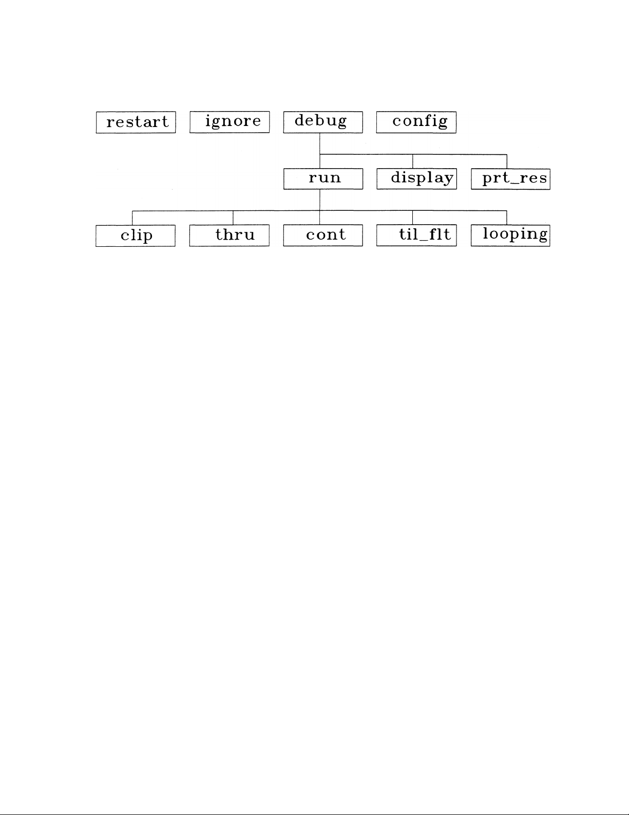
The Debug mode is used for observing selftest results, running selftests and printing results. It
may be entered, after a successful selftest, by pressing ES(system) IH) EXdebug) from the main
screen of the initial level. Debug is accessible directly after a poweron selftest fails. The menu
tree for the Function Keys after a fail spears as:
Key labels and they are represented in this manual as: (ES(label).
as: l enter j. Operational modes progress down a tree
1 -1
Page 10
Service Manual Introduction FLUKE 900 SERVICE MANUAL
©(restart) will re-execute the poweron selftest.
©(ignore) will bring up the main screen directly. If any of the failed selftests involve actual
testing circuitry (eg. FMxx), the operator will not be permitted to actually run a test cycle. File
manipulation, RD Test and System setting changes are possible, however.
Debug has three main keys: ©(run), ©(display), ©(prt_res). The last one means "print
results" and sends a formatted listing of all test results from the last test(s) executed to the serial
RS232 port, "display" brings to the screen, the characteristic 4 b)4e in^vidual result of the test
whose number was entered on the command line. This test must first have been run, either
explicitly or during the powerup.
The key labels under "run" are words that can be used to compose a command line instmction.
Some typical instmctions are:
Rim_test clip
Run test 0
Run test 40
Run_test 1 thm 40
Run test continuous
Run_test 46 continuous
until_fault
Run_test 1 looping
These two equivalent instructions run the clip continuity test.
A clip must be inserted in the Input Bufter and clipped onto
the Dummy Chip Module which must be plugged into the
ZIF socket. Results are shown on the screen.
Test 40 is executed and result bytes displayed in the case of a
failure.
Tests 1 through 40 are executed successively.
The series of poweron tests are executed repeatedly with the
number of passed and faUed cycles displayed on die screen.
will terminate it upon completion of the currently
executing test. This is a useful bumin procedure.
Test 46 is executed repeatedly while displaying the number of
passed cycles until the point at which a failure occurs.
Test 1 win execute repeatedly to facilitate signal tracing with
an oscilloscope.
1 -2
Page 11

FLUKE 900 SERVICE MANUAL Service Manual Introduction
At any point in the menu tree or any operational mode of the tester, a hard or soft reset may be
executed. Pressing (shift] and (^) simultaneously causes a soft reset that returns the display to
the initial power-on screen. This action does not erase any files that are resident in volatile
system RAM. For service purposes a soft reset during selftest is a convenient way to truncate the
selftest and bring up the main screen immediately. Pressing
a hard reset that clears memory and restarts selftest.
There is a special keyboard mode used mainly for calibration called the "engineering menu". It
may be entered from the main poweron screen by simultaneously pressing (cisto) and an
unlabeled key found between and (testJ. Its use will be described in the section on
calibration.
(cnthj and simultaneously causes
1 -3
Page 12

Service Manual Introduction
This page intentionally left blank.
FLUKE 900 SERVICE MANUAL
1 -4
Page 13
FLUKE 900 SERVICE MANUAL
Theory of Operation
2 Theory of Operation
2.1 General
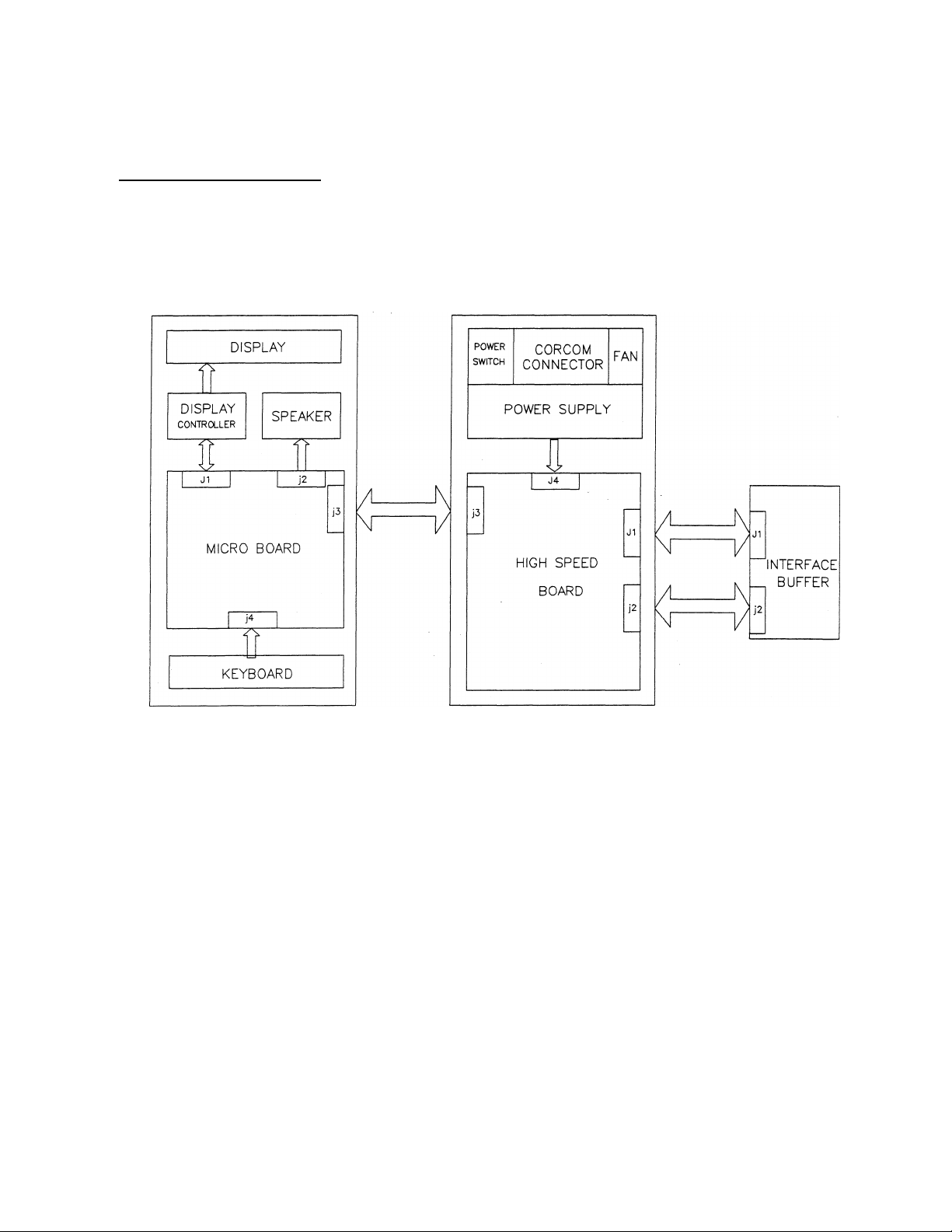
Major functional blocks of the tester correspond, in general, to physical modules. Shown below is
a diagram of the modules and their interconnections.
The Interface Buffer (IB) acquires and conditions signals from the board under test. It accepts 28
signal channels from an interchangeable clip and, by means of a single threshold setting,
translates them into ECL digital data for transmission to the High Speed Board.
The Micro Board (MB) controls the operating system, user interface and test parameter storage.
The Micro Board has a Z80 microprocessor running from about 320K of paged memory space.
The software is mainly comprised of interrapt routines that service four 8536 CIO devices. Two
CIOs are on the MB, the "Keyboard" and "Map" devices, while two CIOs are on the HSB, the
"Time" and "Frequency" devices.
The Micro Board sets up the High Speed Board (H3) with the proper configuration for a test
before letting it run at high speed without intervention. The setup of the test proceeds by loading
a series of shift registers with data impropriate for the test to be performed. Four 8 bit registers
are cascaded to make a set of 32 bits in length. Six such sets are located on the H3, two on the IB.
2-1
Page 14

Theory of Operation
During the test phase, signals received by the H3 are routed immediately to a comparison circuit
to be matched against one of two possible signals. In the case of a signal extracted fix)m a DUT
input pin, the comparison is made with itself ( no failure should appear ). In the case of a DUT
output pin signal, the comparison is made with the identical RD pin signal. The RD pins are
continuously monitored by a resistive load to determine whether tiiey are input or output and
thus how to route the equivalent DUT signals. At each signal transition, the DUT/RD
discrepancy is timed to see if it exceeds a set FMASK value. If so, and if not overridden by a Gate
or Trigger setting, the faults are latched and displayed on the monitor LEDs and LCD Screen.
FLUKE 900 SERVICE MANUAL
2.2 Interface Buffer
Pages 3,4,S,6 of the IB schematics show the signal path for each of the 28 channels that can come
from a DUT. lOK resistors connect each channel to an output bit on the cascaded shift registers
shown on page 1. In actual usage, these are resistors pulled up to 5 volts by default to resolve
floating imconnected inputs on a UUT which could otherwise confuse test results. In addition,
the check for a low condition on a pin is made while attempting to pull it high; the high check is
made with the lOK resistor pulled down to ground.
After the impedance matching components and protection diodes, each chaimel feeds a
comparator referenced to a bias voltage. The ouqjuts are differential E(X levels for relative
noisefiee transmission to the High Speed Board.
The shift registers shown on page 2 are used to control the bias setting for threshold, the Reset
line setting and external frequency multiplexing. Eight bits drive a DAC which resolves a 0 to 5
volt range into 100 mV increments. Five bits control the polarity, voltage and status of the Reset
driver (Page 1). Three bits route one of several lines through an analog multiplexer to a
voltage-controlled oscillator (U25). The measurement of the VCO frequency on the HSB is used
to determine clip size ( from a characteristic voltage divider in each clip), threshold verification
and VCC accuracy.
2-2
Page 15

FLUKE 900 SERVICE MANUAL
Theory of Operation
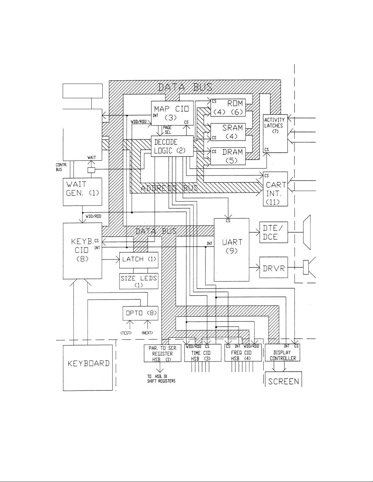
2.3 Micro Board
The Micro Board architecture is shown in the accompanying diagram. Note that, for
simplification, bus buffers are not shown and all chip select signals are shown as CS to a device
instead of the actual signal ( eg. CS for MAP CIO is actually MAPSEL ). The Z80 CPU runs at 6
MHz and operates with the Wait State Generator PAL (U69) to give the delayed control signals
WRD and RDD. The CPU signals WR and RD are thus modified for the timing requirements of
the Display Controller and the 8536 CIO chips. The four CIO devices are complex counterAimer
and parallel I/O ports. Two are located on the MB, two on the HSB, and they interrupt the CPU
for servicing of their particular function.
The MAP CIO sets up the memory map and paging scheme through PALs U58, U59, U72, U73.
Port A is configured as output for the PAL chip selects. Port B is output for the EPROM chip
selects. Port C is output for the RAM chip selects. The internal timer on this CIO is used for
general timeout purposes in such functions as cartridge operations and library loading.
The Decode Logic consists of the PALs referred to previously and it generates chip selects for all
peripheral devices and extends the 64K address range of the Z80 as shown in the memory mt^
diagram.
The first 16K is the power on
boot ROM space (ROM
SYSAF is part of it). The
next 8K of CPU address
space is used to access 14
pages of 8K in size residing
on the SYSAF and B ROMs.
The next 8K starting at
address 6(X)0 accesses 14
pages residing on SYSC and
D ROMs. The range 8000 to
COOO is 16K of static RAM.
The first RAM chip has a
battery and retains the
System Mode option
parameters. It also has 8
pages of cartridge memory
and 16 pages of library
ROM. The final 16 K is
overlayed with 4 pages
comprising the DRAM and
used for internal functions
and 48K of ":SYST"
sequences.
4000
6000
8000
AOOO
COOO
FFFF
16k
SYSAF
8k
OVERLAY
8k
OVERLAY
8k
SRAM
8k
SRAM
15k
DRAM
Ci;234S6iS9ABCiQ
C i:24436789A8GD
I N : i M M :; M pages SYSD
i|234S67aT234367a3ABGDEF g
j 15 pages library
23
4 pages rSYST
14 pages SYSAF
14 pages SYSB
14 pages SYSC
The Keyboard CIO outputs levels on port A which are read back on port B when a key is
depressed. Three internal timers designated "watchdog", "key_time" and "key" take care of
2-3
Page 16

Theory of Operation
debouncing and repeating key actions. The itest) and inext) keys found on the Interface Buffer
are routed through the HSB and optocoupled on the MB to connect to the keyboard CIO. The
chip size LEDs are driven by a latch controlled by this CIO.
The dual UART located at Ull is used for two functions. First, the serial RS232 interface is
connected through a DTE/DCE selectable routing circuit so it can interface to various computers
and printers. Second, various standard frequencies are generated to drive a speaker providing
audible beep tones. The socket at U62 contains the battery and circuit for the real time clock
function.
FLUKE 900 SERVICE MANUAL
2-4
Page 17
FLUKE 900 SERVICE MANUAL
MI CR D BOARD A RCHI TEC TU RE
Theory of Operation
□sc
CPU (1)
\/
(1)
INT
TESTDN
MDN BUS
(MSB)
CARTRIDGE
RS232
SPKR,
H I G H S P EED B E AR D
2-5
Page 18

Theory of Operation FLUKE 900 SERVICE MANUAL
2.4 High Speed Board
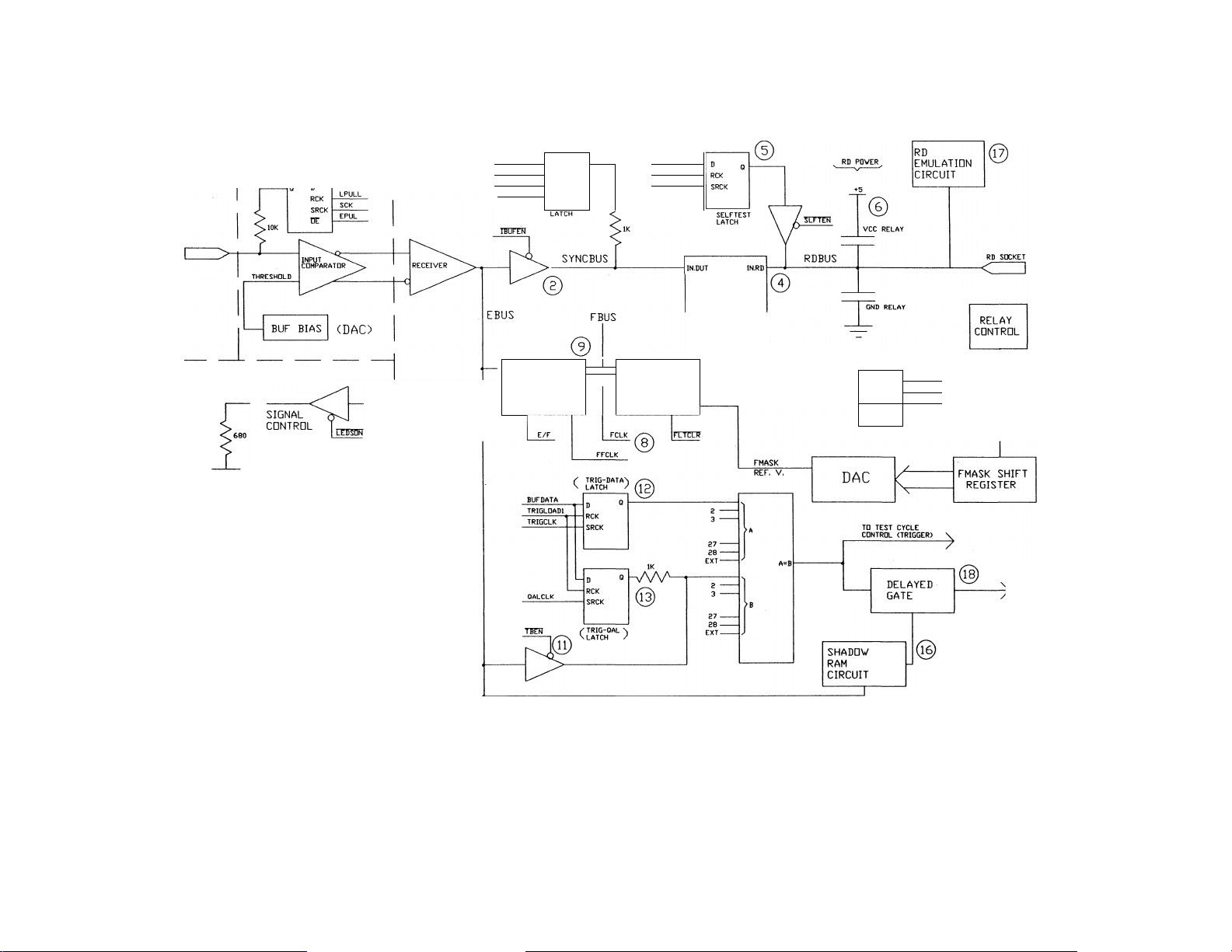
The accompanying diagram shows one chamiel routing a signal from the test clip through the
Interface Buffer to the High Speed Board (H3) where it is processed by Dynamic Reference
Comparison. The Micro Board then receives indicators from the H3 to display a test result There
are 28 such channels in parallel. The circuit elements that are depicted as latches in the diagram
are implemented with shift registers that are first serial loaded, then clocked to a parallel ou^t
latch. The diagram’s latches are single bits of a 28 bit shift register comprised of four cascad^ 8
bit 74595s.
2-6
Page 19
TEST
CLIP
INPUT BUFFER
MICRO BOARD
'f-
.-UPS
©
ACTIVITY
MONITDR
HIGH SPEED BGARD
BUFDATA
w
SYNCLÖAD
SYNCCLK
SYRCEN
° Q
RCK
SRCK
SYNC
_____
©
BUFDATA
SLPTLOAÖ
SLFTCLK
C
m
CO
o
o
CO
m
3J
<
o
DIFTEST
BUFFER
□UT <DC)
m
>
z
c
>
MGNBUS
EBUS.IN FAULT.IN
LATCHING
CIRCUIT
OUT
SELECT
\ /
OUT
FRAMING IN
CIRCUIT
CLEAR
vw— °
PIN-DIS
LATCH
SRCK
RCK
©
BUFDATA
öiSloaü
DISCLK
.TO TEST CYCLE
7 CONTROL
ro
•nI
(14)
(D
“O
O
O
O
CD
O
3
FREQUENCY
COUNTER
CMUX)
EXT-
I
GATE-
10)
Page 20

Theory of Operation
The busses shown are as follows:
EBUS
External bus represents DUT signals after conversion to TTL levels using a single
threshold in the IB. EBUS is labelled on pages 2, 4, 6, 8, 9, 10, 11 of the H3
schematics.
RDBUS
Reference device bus carries EBUS input pin signals to the RD socket and RD
output pin signals to the DIFTEST circuit. RDBUS is labelled on pages 7, 8,9,10,
11 of the H3 schematics.
EBUS
Fault bus indicates on which pins the RDBUS and EBUS were different for longer
than the FMASK value. The FBUS consists of the op amp ouQ)ut signals labelled
Fxxon pages 8,9,10,11 of the H3 schematics.
SYNCBUS
Synchronizing bus is either the EBUS or a pattern from the device library,
depending on whether the Sync Vectors technique is employed to synchronize RD
and DUT. The SYNCBUS consists of the 74244 output signals found on the
extreme left side of pages 8,9,10,11 of the H3 schematics.
FLUKE 900 SERVICE MANUAL
MONBUS
Monitor bus is either the same as EBUS or FBUS, depending on which is selected
for display on the monitor LEDs. The Mon bus may be found at connector J3 on
the right side of pages 8,9,10,11, of the H3 schematics and on page 13 of the MB
schematics.
The 18 circuit blocks shown in the diagram on the previous page are the same ones listed across
the top of the Selftest/Circuit Block Reference Table (Section 4.2). Fifteen of the blocks
described below are found on the H3 Board.
1.
PuUups Latch
On the Interface Buffer, signals from the test clips are pulled up to VCC or down
to Gnd through a lOK resistor from the output of this shift register latch. It is found
on page 1 of the IB schematic, Ul, U2, U3, U4. The register at U24 of the BB drives
a DAC which sets the threshold.
Inbuf
These buffers found on pages 8,9,10, 11, of the H3 schematics (U186, U140, U95,
U42), feed the EBUS through to the SYNCBUS. They are tristated when the Sync
Latch is driving.
Sync Latch
Synchronizing patterns from the library data are shifted ink) the registers shown on
pages 8,9,10,11, (U182, U136, U91, U45) and then latched to the output as a test
vector. The stimulus for the RDTest ftmction is provided in the same way.
2-8
Page 21

FLUKE 900 SERVICE MANUAL Theory of Operation
Diftest Buffers
This circuit uses one of two possible resistor values (Hi or Lo) to determine
whether the RDBUS can drive and therefore whether the pin is an output The
final output indicates the discrepancy between RDBUS and EBUS/SYNCBUS. It
may be foimd at the outputs of the exclusive OR gates on pages 8,9,10,11.
Self Test Latch
The shift register latch used to inject patterns onto the RDBUS during power-on
verification in earlier revison boards is incorporated into the Logic Cell Array at
U105, near the ZDF socket of the H3 Board. This is shown as circirit block 17 on the
block diagram. If a RD is inserted during the power-on test an t^arent failure will
result
RD Supply Relays
Certain ZIF socket pins are cormected to VCC or Gnd by closure of the relays
shown on page 7. The shift registers U155 and U102 control their selection.
Pin Dis Latch
These shift register latches can override the fault indication output from the Diftest
circuit to ignore a fault on a pin. They are shown on pages 8, 9, 10, 11, as U180,
U134, U89, U40.
8.
9.
10.
11.
FFCLK Line
The CPU can simulate a fault by asserting this line which is ORed with the pin fault
lines to produce FLTS, the master fault indicator (page 11, A-10). Shift register
U67 (page 3) provides data to a DAC which provides the FMASK reference
voltage used in the framing circuit. The charging of precision capacitors to this
voltage establishes an FMASK value. Note that ttie 74ALS09s driving the
capacitors are specially prescreened to be uniform.
Mon Mux
The latches at U198, U153, U112, U64 hold the individual pin faults. The PALs
driving them are also latches which accumulate faults for 40 ns after the first line
fails but no further. In this way, the results are frozen in a window around the first
fail for later reading by the CPU over the Mon Bus. When no faults are present,
the signal M/F selects U164, U122, U76, U43 (pages 8, 9, 10, 11) to route the
EBUS onto the MONBUS.
Freq Circuit
The 8536 CIO at U27 (page 4) controls the multiplexing and measurement of
signal frequency among the 29 channels (28 pins plus 1 external). Port A is
configured as output and used to drive the muxes at U55, U66, U124, U141. Port B
drives the FREQ PAL except for PBS which is an input flagging the occurrence of
Gate. Port C is an input to read the frequency count.
Trig Buf
These buffers U191, U154, U98, U81 on page 2 enable the EBUS to the trigger
comparator when TBEN signal is active.
2-9
Page 22

Theory of Operation
12. Trig Data Latch
The shift register latches U166, U189, UlOO, U78 are loaded with data indicating Is
and Os of the Trigger word. The first word is serial shifted and latched followed by
the second word which is not latched until the occurrence of the first.
13. Trig Qual Latch
The shift register latches at U168, U188, U96, US6 are loaded with data indicating
which pins have a 1 or 0 and which have "don’t care" conditions. Two successive
words are loaded as in the Trig Data case.
14. Activity Circuit
This circuit on page 7 of the Micro Board schematics operates by latching the state
of all pins at the start of test and generating an exclusive OR pulse if the state ever
changes, hi this way, the PALs U32, U21, U16, U22 are alerted of active pins.
15. Mon Bus Readback
The Mon Bus which comes from the ffigh Speed Board to the Micro Board via the
connector J3 is shown on page 13 of the MB schematics. The latches and PALs on
page 7 use the Mon Bus to hold the state of all pins at the end of test (for the EoT
test result). The state of pins at the start of test is also latched here for the purpose
of checking H or L conditions on DUT pins.
FLUKE 900 SERVICE MANUAL
16,18. Shadow Ram and Delayed Gate Circuit
This circuit is implemented in the Logic CeU Array at U123 (page 6) and associated
PALs. Both of these functions affect the gating of comparison. Shadow RAM
inhibits comparison during reading of an uninitialized DUT memory cell. Delayed
gate inhibits the normal gate signal from going true for a fixed time interval after its
pin conditions are satisfied.
17. RD Emulation Circuit
This Logic Cell Array, located at U105 (page 12), simulates certain Reference
Devices instead of using an RD in the socket. If an H3 Board does not have the
Simulation Option instafied, U105 is still present to perform selftest functions.
Test cycle control is applied to all 28 channels together and is found on page 3 of the H3
schematics. The Time CIO at U26 is configured so РАО, 1,2 enable the Trigger flip flops and
GATE PAL. РАЗ is an output for enabling comparison during selftest. PA4 is an input that
detects whether gate occurred. PA5 is an input indicating a short in the RD socket. PA6, 7 are
inputs that detect whether trigger word 1 and 2 occurred.
Port В controls the Test Cycle PAL; PBl is an input which stops test after a fault has been
captured. PB2, 3, 4, 5 are inputs from a counter which acts as a prescaler for the time-to-fault
interval. An internal CIO timer converts it to a value in the proper range. PB6 is an output that
clears the fault under CPU control, while PB7 is an input indicating a fault is present Port C is
configured as an output and it selects which shift register will receive the data stream from the
register U36 on page 1 of the H3 schematics.
2-10
Page 23

FLUKE 900 SERVICE MANUAL
Theory of Operation
2.5 Test Clips
The standard Test Clips have no active components, but the ribbon cable is temiinated at both
ends with a series 300 ohm resistor for impedance matching. There are 10 Kohm puUup resistors
in the Interface Buffer which are applied to the DUT through the 600 ohms of the Test Clip.
The High Impedence Test Clip has an active buffer at the clip head which presents 500 Kohm
impedence to the DUT. The clip head is powered from the VCC pin of the DUT.
2-11
Page 24

Theory of Operation
This page intentionally left blank.
FLUKE 900 SERVICE MANUAL
2-12
Page 25

FLUKE 900 SERVICE MANUAL
3 Selftest
3.1 Reading Selftest Results
Immediately after poweron, the tester executes a series of selftests that take about one minute.
The selftests may also be initiated at any time by simultaneously pressing (.cntrj and (^. The
tests are number^ 0 to 55 and all but a few are run automaticaUy. These few plus a number of
"extended tests" denoted by Exx (eg. E60), can be run by manually keying them in when analyzing
a problem. All the tests may be run individually in this way to produce "individual test results".
When a failure is encountered during poweron selftest, two rows of digits display "general results"
and sometimes a third and fourth row appear. Rows 1 and 2 indicate the failing test numbers;
rows 3 and 4 indicate fault flags that are tied to memory and shift registers. Flag failiues indicate
major functional problems and general test results indicate which tests are failing. "Individual test
results" are more detailed dispays of the failing tests and they indicate which channels (lines) ate
faulty.
In cases where a failure is severe and the LCD screen may not function, the LEDs around the
ZIF socket may indicate the problem.
Selftest
Hardware and software problems occasionally result in system crashes that present a message on
the command line. One cause of such a crash is a corrupted simulation library file. A summary of
these messages appears in Section 3.4.
3-1
Page 26

Seiftest
FLUKE 900 SERVICE MANUAL
3.1.1 General Selftest Results
The general results on the first two lines are clustered in groups of five as shown in the
example below. The test numbers are shown above and below the digits. 0 indicates Pass, 1
indicates Fail and X indicates that a test result is not available.
0-4 5-9
XOOOO 00000
00000 01000 00011
30-34
The cross reference of test numbers to test names is listed below:
SLFT CLIP
0
PULLO_MON 30 FM40_NFLT
1
PULLl MON
2
PULLO.FLT 32 FM80_NFLT
3
PULLl FLT
4
SYNCO Hres FLT
5
SYNCl Hres FLT
6
SYNCO Lies FLT
7
SYNCl Lres.FLT
8
PINDISO FLT
9
PINDIS1_FLT 39
10
SLFTSTO FLT
11
SLFTSTl FLT
12
VccON FLT 42 PULLO ACT TSTON
13
GndON FLT
14
PULLPOS FREQ
15
TRIGQALO EQUAL
16
TRIGQALl EQUAL
17
qalo_equal 47
18
QALl EQUAL
19
TRIGO EQUAL
20
TRIGl EQUAL
21
PULLO TRIG EQUAL
22
PULLl TRIG EQUAL
23
PULLO TRIGQAL
24
FM_STAT_NFLT
25
FM STAT FLT
26
FMASK WB_TEST
27
FMASK CAL
28
35-39
10-14
mil
40-44
15-19 20-24
00000 00000 OXXll
XXX11
45-49 50-54
25-29
11100
XXXXX
55-59
29
FM40 FLT
FM80 FLT
31
33
FM120 FLT
34
FM120 NFLT
FM160_FLT
35
36
FM160 NFLT
37 FM200.FLT
FM200_NFLT
38
FM240 FLT
40 FM240 NFLT
41
ACT DIS CLR
PULLl ACT TSTON
43
44
PULLO ACT ACTSTR
45 PULLl ACT ACTSTR
46
FREQ_BIAS SHORT
FREQ_BIAS_LONG
48 KEYBOARD OPEN
49 TEST_CYCLE
50 UART.TEST
DGATE TEST
51
52
PULLO.XTRIG
53 PULLl XTRIG
54
PULL_XEVENT
SHAD.INTT
55
3-2
Page 27

FLUKE 900 SERVICE MANUAL
Tests 0,47 and SO are not automatically run during the poweran selftest, but can be nin by
themselves explicitly. This is also the case for a group of tests known as "engineering" or
"extended" tests which are designated Exx as follows:
Seiftest
E60
E61
E62
E63
E64 SHAD ADDR
E70
E71
E74 DISP CHAR SET
E75
E76
E77
E78
E79
E80
2 Flag
Flags may ^pear on lines 3 and 4 of the general results screen. A 0 means "OK" and a 1
means "fault". At the present time, only the first row is used.
WALK SIZELEDS
TEST MEMORY
WALK MONLEDS
UPDATE_VCC_UM
KEY CLOSURE
DISP RAM
CART_SLFT
TEST C ENG
ACT_CROSS
TRG CROSS
FRQ_CROSS
FLT_CROSS
Results
BYTEO
I
00000000
00000000
BYTEl BYTE2
I I
00000000 00000000
00000000 00000000
BYTE3
I
00000000
00000000
11111111
BIT: 76543210
BYTEO: Indicates DRAM chip which failed memory test
B7: U86
B6: U82
B5: U87
B4: U83
B3: U88
B2:U84
Bl: U89
BO: U85
3-3
Page 28

Seiftest
FLUKE 900 SERVICE MANUAL
BYTEl: Indicates shift register bank which failed
B7: INTERFACE BUFFER OB U1,U2,U3,U4)
B6: DELAYED GATE
B5: SELFTEST (HSB U38,U76,U115,U150)
B4: FMASK (HSB U72)
B3: TRIGGER QUALIFIER (HSB U57,U87,U142,U162)
B2: TRIGGER DATA (HSB U66,U91,U140,U163)
BLPIN DISABLE (HSB U41,U80,U119,U154)
BO: SYNC (HSB U46,U82,U121,U156)
BYTE2: General
B7; NVRAM bad
B6: NVRAM checksum error, rewritten with default data
B5: Not used
B4: Not used
B3: ROM bad (U77)
B2: ROM bad (U76)
Bl: ROM bad (U75)
BO: ROM bad (U74)
BYTE3: General
B7,6,5,4: Not used
B3: FMASK calibration error
B2: Threshold calibration error
Bl: FLTS line not readable
BO: Threshold setting error
3-4
Page 29

FLUKE 900 SERVICE MANUAL Selftest
3.1.3 Chip Size LED Error Codes
If self test fails, on rare occasions, the chip size LEDs may light to indicate an error. In the list
below, the 8 LEDs are shown with a 0 for unlighted and a 1 for lighted.
00000001: KEYBOARD CIO PortA. CPU cannot communicate.
00000010: KEYBOARD CIO PortB
00000011: TIME QO PortA
00000100: TIME CIO PortB
00000101: FREQ CIO PortA
00000110: FREQ CIO PortB
00000111: Display not ready
00001000: ROM checksum error
00001001: SRAM error
00001010: Stack underflow
00001011: Unimplemented interrupt occurred
00001100: Invalid intermpt vector
00001101: Not used
00001110: Incorrect peripheral serviced
00001111: UART transmit error
00010000: UART other errors ( special receive conditions)
00010001: UART parity error
00010010: DRAM error
00010011 : Overlay error
00010100: Not used
00010101: MAP CIO PortA
00010110: MAP CIO PortB
00010111 : Display memory error
3-5
Page 30

Seiftest
FLUKE 900 SERVICE MANUAL
3.2 Running and Reading Individual Selftests
The individual selftest results indicate which specific lines or channels are failing. A full printout
of all failing individual results may be printed out as explained in Section 1.2. Altemativdy, a
single individual result may be viewed on the display by pressing the following keys after the
general poweron seUtest fails: ED(debug) ©(display) "test #" ien^j. The individual result then
appears as £010* bytes with a 1 indicating a problem.
BYTEO
BYTEl
I
00000000 00000000
BIT: 76543210 76543210
BYTEO
b7:X
b6:X
b5:X
b4: EXT LEAD
b3: PIN 1
b2: PIN 28
bl: PIN 2
bO: PIN 27
Refer to the individual descriptions of Section 3.3 for any bit assignments that may differ fixm
those generaEy used above. In particular, bits 5,6,7 of BYTE 0, which are not used for most tests,
may have a meaning which is noted for a specific test
BYTEl
b7: PIN 3
b6: PIN 26
b5: PIN 4
b4: PIN 25
b3: PEST 5
b2: PEST 24
bl:PESr 6
bO: PIN 23
BYTE2 BYTE3
I I
00000000 00000000
76543210 76543210
BYTE2
b7: PEST 7
b6: PEST 22
b5: PESf 8
b4: PIN 21
b3: PEST 9
b2: PTN 20
bl: PEST 10
bO: PIN 19
BYTE3
b7:PIN 11
b6: PIN 18
b5: PIN 12
b4: PB4 17
b3: PEST 13
b2: PEST 16
bl: PIN 14
bO: Pm 15
3.3 Individual Selftest Descriptions
3-6
TEST 0 SLFT_CLIP
The SLFT_CLIP routine is used for verifying test clips. The test clip in question is inserted
into the Interface Buffer and the other end is inserted into the ZEF RD socket via the Test
Oip Verification Module. When the test is running, die size of the current test clip is
displayed. The failure information is displayed as follows (Only special bits are shown, all
others refer to tegular pin number):
BYTE 0 - B7 -
B6B5B4-
Not used
Not used
Clip size code invalid
Frequency reading invalid
Page 31

FLUKE 900 SERVICE MANUAL
TESTS 1 2
PULLO_MON, PULL1_MON
These tests supply a walking 0 or 1 across all lines from the pull-tq)s latch, through the iiqnit
buffer, to the MONBUS where the levels are read by the (TPU.
TESTS 3,4
PULL0_FLT, PULL1_FLT
These tests supply a walking 0 or 1 across all lines fixnn the pull-ups latch, through die iiqnit
buffer, through the fault circuitry to the MONBUS where the levels are read by the CPU.
TESTS 5,6
SYNCO_Hres_FLT, SYNCl_Hres_FLT
These tests supply a walking 0 or 1 across all lines from the sync latch, through the HI
resistors, through the fault circuitry to the MONBUS where the levels are read by the CPU.
Selftest
TESTS 7 8
SYNC0_Lres_FLT, SYNC1_Lres_FLT
These tests supply a walking 0 or 1 across all lines from the sync latch, through the LO
resistors, through the fault circuitry to the MONBUS where the levels are read by the CPU.
TESTS 9,10
PINDISO_FLT, PINDIS1_FLT
These tests supply a walking 0 or 1 across aU lines from the pin disabling latch, through the
fault circuitry to the MONBUS where the levels are read by the CPU.
TESTS 11,12
SLFTSTO_FLT, SLFTST1_FLT
These tests supply a walking 0 or 1 across all lines from the selftest latch, through the fault
circuitry to the MONBUS where the levels are read by the CPU.
TESTS 13,14 VccON_FLT, GndON_FLT
These tests walk the Vcc or Gnd relays on. Their operation is verified through the fault
circuitry to the MONBUS where the levels are read by the CPU.
3-7
Page 32

Seiftest
FLUKE 900 SERVICE MANUAL
TEST 15
PULLPOS_FREQ
This test walks a positive pulse through the pull-ups latch to tiie frequency circuitry,
TESTS 16,17
TRIGQALO_EQUAL, TRIGQAL1_EQUAL
These tests walk a 0 or a 1 through the trigger and qualifier latches and the results are
determined through reading the EQUAL line.
TESTS 18,19
QAL0_EQUAL, QAL1_EQUAL
These tests walk a 0 or a 1 through the qualifier latches and the results are determined
through reading the EQUAL line.
NOTE: For tests 18 and 19, an X in the general test result means that individual
results are imavailable.
TPQT^ Pn P1
TRIGO_EQUAL, TRIG1_EQUAL
These tests walk a 0 or a 1 through the trigger latches and the results are determined through
reading the EQUAL line.
NOTE: For tests 20 and 21, an X in the general test result means that individual
results are unavailable.
TESTS 22 23
PULLO_TRIG_EQUAL, PULL1_TRIG_EQUAL
These tests walk a 0 or a 1 through the pull-ups latches, through the trigger circuitry and are
read through the EQUAL line.
NOTE: For tests 22 and 23, an X in the general test result means that individual
results are unavailable.
TEST 24
PULLO TRIGQAL
This test walks a 0 through the pull-tq>s latches, through the trigger and qualifier circuitry and
the results are determined through reading the EQUAL line.
3-8
Page 33

FLUKE 900 SERVICE MANUAL
NOTE: For test 24, an X in the goieral test result means that individual results are
unavailable.
TESTS 25,26
FM_STAT_NFLT, FM_STAT_FLT
These tests perform a static FMASK test All lines are expected to pass for the "_NFLT" test
while all lines are expected to fail for the "FLT" test
TEST 27
FMASK_WB_TEST
This test does an approximate test using fixed values for FMASK. It uses a tolerance three
times that of the FMxx tests. This test is performed to determine whether or not the FMASK
curve is within a very wide margin.
TEST 28 FMASK_CAL
Selftest
This routine determines the calibration values to be used by FMASK.
TESTS 29,31,33,35,37,39
FMxx_FLT
These tests use a pulse of fixed duration (40, 80,120,160,200 and 240ns) and set FMASK to
just below the duration of the pulse. All lines are expected to produce a fault Those which
do not are flagged as faulty.
TESTS 30,32,34,36,38,40
FMxx_NFLT
These tests use a pulse of fixed duration (40, 80,120,160,200 and 240ns) and set FMASK to
just above the duration of the pulse. AH lines are expected to produce no fault Those which
do are flagged as faulty.
TEST 41 ACT_DIS_CLR
This test checks the disabling and clearing functions of the activity circuitry. It disables the
activity circuit and pulses all lines. Any lines which indicate activity are flagged as faulty. It
also verifies that the activity latches may be cleared and that a single edge on all lines
produces a 1 (activity occurred) in all latches.
3-9
Page 34

Seiftest
FLUKE 900 SERVICE MANUAL
The bits in the tesults indicate nonnal pin numbers with the exception of the following:
BYTE 0 - B7 - NAJ
B6- N/U
B5 - Could not clear PAL latches.
B4 - Could not activate aU lines with a single edge.
TESTS 42 43
PULLO_ACT_TSTON, PULL1_ACT_TSTON
These tests walk a rising edge(l) or a falling edge(0) horn the puU-iq>s latches through the
activity circuitiy. The activity circuit is controlled by the TSTON signal.
TESTS 44, 45
PULLO_ACT_ACTSTR, PULL1_ACT_ACTSTR
These tests walk a rising edge(l) or a falling edge(0) fiom the pull-ups latches through the
activity circuitry. The activity circuit is controlled by die ACTSTR signal.
TESTS 46,47
freq_bias_short, freq_bias_long
These two tests are almost identical, the only difference being that the long test verifies aU
possible values of threshold and the short test only tests at 1 volt increments. The tests are a
collection of several subtests involving frequency and threshold hardware on the High Speed
Board and Input Buffer and they are detiuled below. As they are being done, the left part of
the screen shows timing values from the frequency test and the right side of the screen shows
the highest and lowest differences between expected and measured voltage values.
Many of the subtests require that a voltage on the Interface Buffer be measured. One of
several possible voltages is selected using the analog mux on the input buffer. This feeds the
into the VCO, the output of which is sent to the High Speed Board where the frequency is
measured. The same thing is also done for 0 volts and 2.5 volts to obtain a calibration ratio
that is used to determine the exact voltage of the signal selected.
Interface Buffer shift register subtest
This tests to see if data can be shifted through the shift registers on the Interface Buffer
correctly. There are two banks of registers on the board. Only the puUup registers are
explicitly tested because there is no feedback line from the threshold registers. The
threshold registers are implicitly tested by the other tests. The test procedure is as follows:
a) shift data - msbit = 0
b) read the voltage of the msbit: must be <2V
c) shift data - msbit = 1
d) read the voltage of the msbit: must be >2V
3-10
Page 35

FLUKE 900 SERVICE MANUAL
If this test fails it does not set one of the data bits but rather sets the shifting error flag.
Frequency HW subtest
The frequency hardware tested is on the High Speed Board. It can be configured in
several different ways (the setup for this is shown in the MODE box on the schematic), aU
of which are independently tested.
1. Read a fiequency. A 25MHz clock is generated and the frequency is measured.
2. Read the period. Pin #2 is selected through the frequency mux (this hardware is
tested in a different selftest). It is setup to read the period and then the CPU
generates a cycle of fixed duration on this line using the puUup registers on the
Interface Buffer. The period displayed should be approximately 990 us.
3. Read the high time and low time. These are done in the same way as the period test
except the times are displayed. Low time should be approximately 815 us and high
time 175 us.
Selftest
Threshold HW subtest
This subtest programs a value of threshold and reads it back to verify that it is within an
acceptable range. The variation between the measured value and the value programmed
(in mV) is displayed on the screen. The long test goes through all possible settings
between 0 and 5 volts and the short test only goes in steps of 1 volt
After the threshold setting has been tested the threshold is calibrated to compensate for
input offsets in the comparators. The puUups are used to set the actual threshold on the
input to the comparator to 4.16 and 0 volts and then the threshold is adjusted to see what
offset added to the amount programmed (4.2 and 0 volts) will be closest to the actual
threshold of the comparators. If the adjustment exceeds an allowable amount the
calibration part of this test win fail.
Reset HW subtest
For this subtest the reset relays are set so that power for reset comes from 5 volts and the
output is fed into the analog mux.
a) reset = high: must be > 4 volts
b) reset = low: must be < 1 volt
c) reset = off: must be < 4 volts & > 1 volt
3-11
Page 36

Seiftest
Result bytes:
BYTE 0
b7b6b5b4b3-
b2bl -
bO-
BYTE 1
b7b6b5-
b4b3b2-
bl-
bO-
0
0
0
0
Threshold calibration failed. Ignore this bit unless the other bits in this byte
are clear. If they are clear and this bit fails the output of the threshold Op
Amp has too great an offset
Unable to complete test. Something is wrong with the CPU - CIO interface.
The threshold was too high. The output of the Op Amp was greater than
expected by more than the allowable amount
The threshold was too low. The ouQnit of the Op Amp was less than
expected by more than the allowable amoimt
Vcc(IB) is too high ( > 5.2V ). The main Vcc voltage as read at the
Interface Buffer is too high. If this test fails, ALL other selftests are invalid.
Vcc(IB) is too low ( < 4.84V ). The main Vcc voltage as read at the
Interface Buffer is too low. If this test fails ALL other selftests are invalid.
0
0
0
Unable to turn off the reset line. The reset output fiom the Interface Buffer
could not be made to go tri-state.
Unable to drive the reset line low.
Buffer could not be made to go low.
Unable to drive the reset line high.
Buffer could not be made to go high.
FLUKE 900 SERVICE MANUAL
The reset output from the Interface
The reset ou^ut from the Interface
3-12
BYTE 2
b7-
b6-
b5b4b3-
Period measured was too long. There are several possible causes. The
25MHz crystal could be oscillating at the wrong frequency, the WSG pal
could be faulty, almost any of the 4 frequency chips could be bad.
Period measured was too short. There are several possible causes. The
25MHz crystal could be oscillating at the wrong fiequency, the WSG pal
could be faulty, almost any of the 4 frequency chips could be bad.
No results obtained from period read. The test has timed out. Something is
wrong with the CPU - CIO interface.
Unable to set up the period read. Something is wrong with the CPU - CIO
interface.
HW oscillator (25MHz) is too fast. There are several possible causes. The
25MHz crystal could be oscillating at the wrong frequency, almost any of the
4 frequency chips could be bad, the 2925 clock generator could be bad, there
could be a problem in the fiequency muxes.
Page 37

FLUKE 900 SERVICE MANUAL
b2 - HW oscillator (25MHz) is too slow. There are several possible causes. The
25MHz crystal could be oscillating at the wrong frequency, almost any of the
4 frequency chips coiild be bad, the 2925 clock generator could be bad, there
could be a problem in the frequency muxes.
bl - No results obtained from freq read. The test has timed out Something is
wrong with the CPU - CIO interface.
bO - Unable to set up the frequency read. Something is wrong with the CPU -
CIO interface.
BYTE 3
b7-
b6-
b5
b4
b3
b2-
bl
bO
The active low duty cycle measured was too long. There are several possible
causes. The 25Nfflz crystal could be oscillating at the wrong frequency,
almost any of the 4 frequency chips could be bad, the WSG pal could be
faulty, the 2925 clock generator could be bad, there could be a problem in
the frequency muxes.
The active low duty cycle measured was too short. There are several possible
causes. The 25MHz crystal could be oscillating at the wrong frequency,
almost any of the 4 frequency chips could be bad, the WSG pal could be
faulty, the 2925 clock generator could be bad, there could be a problem in
the frequency muxes.
No results obtained from low read. The test has timed out. Something is
wrong with the CPU - CIO interface.
Unable to set up the low read. Something is wrong with the CPU - CIO
interface.
The active high duty cycle measured was too long. There are several possible
causes. The 25MHz crystal could be oscillating at the wrong frequency,
almost any of the 4 frequency chips could be bad, the WSG pal could be
faulty, the 2925 clock generator could be bad, there could be a problem in
the frequency muxes.
The active high duty cycle measured was too short. There are several
possible causes. The 25MHz crystal could be oscillating at the wrong
frequency, almost any of the 4 frequency chips could be bad, the WSG pal
could be faulty, the 2925 clock generator could be bad, there could be a
problem in the frequency muxes.
No results obtained from high read. The test has timed out. Something is
wrong with the CPU - CIO interface.
Unable to setup the high read. Something is wrong with the CPU - CIO
interface.
Selftest
3-13
Page 38

Seiftest
FLUKE 900 SERVICE MANUAL
TEST 48
KEYBOARD_OPEN
This test verifies that all keys are in the open state including the keys on the buffer. The last
two bytes of the individual test result will contain two set bits which may be intetpreted from
the following matrix to identify the key that was depressed.
KEYBOARD MATRIX
byte 3—> b7
2
I
J4| 16 I
V
bO
bl
b2
b3
b4
b5
b6
b7
1 I G I A I ESC I SHFT I CNTR | Y | S | M
2 I II C I F2 I space I < , I = + I U | 0
3 1 K I E I F5 |BoL<- I PgUp ''I : ; I W | Q
41 LI F I F4 |EoL-> |PgDn v| ? _ I X | R
5 I # 3 I ! 1 I ETC I ENTER |sparel| ( 9 | & 7 | %5
6 I $ 4 I § 2 I NEXT I TEST |spare21 ) 0 | * 8 | "6
7 I J I D I F3 I spares I > . I / - I V | P
8 I HI B I FI I CE I |<—>1 I Z I TIN
TEST 49 TEST_CYCLE
b6 b5
15 1
14 1 13
b4
b3
1 12
b2
1 11
bl
1 10
bO
1 9
3-14
This test verifies that:
- the following lines are not broken or shorted:
/SYNCEN
/SHORT interrupt line
/RELEN
- the following timers are good:
Test time timer
10 ms system timer
1 ms free rumiing timer
- gate and trigger work properly
Page 39

FLUKE 900 SERVICE MANUAL
/SHORT is checked to see if the line is hi^ (ie. not shorted to ground). /SYNCEN and
/RELEN are tested by having sync latches or relays cause a fault and verifying that the fault
occurred.
Four bytes of test results are presented:
BYTE 0
b7 thru 5-0 (not used)
b4 -/STRFRQ output ofTC PAL not woiking
b3 - Interrupts failed
b2 - /SYNCEN line test failed
bl - /SHORT test failed
bO - /RELEN test failed
NOTE: only interrupts generated by TIME port are tested.
BYTE 1
b7 thru 3 - 0 ( not used )
b2 - test time timer
bl -10 ms timer
bO -1 ms timer
Selftest
Each bit in bytes 2 and 3 corresponds to one execution of the test cycle, set up to produce the
expected results. If any bit in bytes 2 or 3 is set it means that results were not as expected. For
example, if b6 in byte 2 is set it means that the gate function was observed to be not active or
faults were detected. Trigger is programmed with one word Gevel) in byte 2 trigger test; for
byte 3, trigger is programmed with two words (edge). For aU W2 related tests (byte 3 bits 3
thru 0), W1 always occurs.
BYTE 2
b7 - gate did not occur no faults
b6 - gate occurred no faults
b5 - gate did not occur, fatilts
b4 - gate occurred, faults
b3 - trigger did not occur, no faults
b2 - trigger occurred, no fault
bl - trigger did not occur, faults
bO - trigger occurred, faults
BYTE 3
b7 - trigger W1 did not occur, no faults
b6 - trigger W1 occurred, no faults
b5 - trigger W1 did not occur, faults
b4 - trigger W1 occurred, faults
b3 - trigger W2 did not occur, no faults
b2 - trigger W2 occurred, no faults
bl - trigger W2 did not occur, faults
bO - trigger W2 occurred, faults
3-15
Page 40

Seiftest
FLUKE 900 SERVICE MANUAL
TEST 50
UART_TEST
The RSCNT3, RSCNT2, and RSCNTl lines on the Micro Board control the configuration of
the rs232 port (DTE.DCE). These lines are put into a normally illegal state that allows the
outputs of the UART to be fed into the inputs. This can be done in two ways and all tests are
done in both configurations.
There are two tests: the first tests the control lines (DTR, CTS,...) and the second transmits
data between the transmitter and receiver. The second test is not done if the first fails.
1. Test the control lines (byte 2 & 3 results). Each of the control lines is tested with the
other control line in a fixed state, first hi^ then tested again with it low. At the top of
the results for each byte the setting of the configuration lines is shown. For each test
the state of the state of the two ou^ut control lines is shown as well as the input line
and what state is expected on it
2. Test the data lines. This test is NOT done unless test 1 passes. The baud rate is
programmed to 9600 regardless of the setting of the rs232 port. At the end of the test
it is reprogrammed with the correct value. A small block of data is sent and compared
with what was received. The receiving of data is interrupt driven so that this test may
fail if there is something wrong with this part of the board. The setting of the
configuration lines is shown for each test.
RESULT BYTES
BYTE 0 = all bits 0
BYTE 1
b7-0
b6-0
b5 - 0
b4-0
b3-0
b2 - 0
bl -1 if serial data test failed with RSCNT[3,2,1]=001
bO -1 if serial data test failed with RSCNT[3,2,1]=110
NOTE RSCNT[3,2,1] means that control signals RSCNT3, RSCNT2, RSCNTl to Ul,
U2, U7 on the Micro Board (page 9 of schematics) were held in the states shown
during the test.
3-16
Page 41

FLUKE 900 SERVICE MANUAL
BYTE 2 -RSCNT[3,2,1] = 001
b7-DTR=0, RTS=1, test for CTS=1
b6 - DTR=0, RTS=0, test for CTS=0
b5-DTR=l, RTS=1, test for CTS=1
b4 - DTR=1, RTS=0, test for CTS=0
b3 - DTR=0, RTS=0, test for DCD=0
b2 - DTR=1, RTS=0, test for DCD=1
bl - DTR=0, RTS=1, test for DCD=0
bO - DTR=1, RTS=1, test for DCD=1
BYTE 3 -RSCNT[3,2,1] = 110
b7-DTR=0, RTS=1, test for CTS=1
b6 - DTR=0, RTS=0, test for CTS=0
b5 - DTR=1, RTS=1, test for CTS=1
b4-DTR=l, RTS=0, test for CTS=0
b3-DTR=0, RTS=0, test for DCD=0
b2-DTR=l, RTS=0, test for DCD=1
bl-DTR=0, RTS=1, test for DCD=0
bO - DTR=1, RTS=1, test for DCD=1
Selftest
TEST 51
DGATE_TEST
This test is performed only if the Simulation Option (900-001) is installed. It verifies the
functionality of the delayed-gate circuit. It checks the operation of the pre-scaler, the delay
function, the duration function and the delayed-gate-activity circuit. Results are interpreted
as follows:
B7
1
_
j
________
BYTEO1
0
1 1
BYTEl1 /15
.667MI1.786MI2•083MI 2.5M 13
|1
BYTE21
1
D U
128
BYTE31
128
1
1 B6
1 0
1 /14
1 64
1 64
D
1
--
1-------------
1DGATE
ACT
1
/12
1
32
1
32
1
B5
R A
E L A Y
B4
1
T
-------------
1DGATE
CLR
1
/10
1
16
1
16
1
B3
1
-4- —
1
1
1
— 4- —.
INF
DUR
/8
.125MI4• 17MI
T
8
1
8
1
B2 1
1
0 1
1
1 DELAY 1
/6 1
1
PRE-
SCALER 1 FAIL
6.25M
I
4 1
1
4 1
1
Bl
1 BO
--l- — — — — — —
1 INVERT
/4
1 /2
112.5M
0 N
2
2
1 1
1 1
3-17
Page 42

Seiftest
FLUKE 900 SERVICE MANUAL
INVERT FAIL
PRE-SCALER
0 DELAYINF. DUR. DGATE ACT DGATE CLR-
Note:
For Example:
Sequence of results during test:
While this test is running in "looping" mode, the expected values and the measured
results are displayed continuously on-screen in the following format (NOTE: Tbe
NEXT key advances to the next part of the test):
Message #
Could not invert gate signal.
A division factor other than one in BYTE 1 failed.
The test for bypassing the delayed gate circuit failed
The test for infinite duration failed (Duration prematurely terminated.
The dgate activity latch failed to register activity.
The dgate activity latch was not cleared by TESTSTR.
Expected
Minimum
140.00 n
Minimum Measured Maximum
Measured Value
160.00 n
Expected
Maximum
180.00 n
Circuitry Tested
#1 24.950 M
#2 12.450 M
#3 8.2833 M
#4 6.2000 M
#5
#6
#7
#8
#9
#10
#11 2.2227 M 2.2727 M 2.3227 M
#12
#13 1.8731 M
#14 1.7357 M
#15
4.9500 M
4.1167 M
3.5214 M
3.0750 M
2.7278 M 2.7778 M 2.8278 M
2.4500 M
2.0333 M 2.0833 M 2.1333 M
1.6167 M
25.000 M 25.050 M
12.500 M 12.550 M
8.3333 M
6.2500 M 6.3000 M
5.0000 M
4.1667 M 4.2167 M
3.5714 M 3.6214 M
3.1250 M 3.1750 M
2.5000 M 2.5500 M
1.9231 M 1.9731 M
1.7857 M 1.8357 M
1.6667 M
8.3833 M
5.0500 M
1.7167 M
Prescaler - divide by 1
Prescaler - divide by 2
Prescaler - divide by 3
Prescaler - divide by 4
Prescaler - divide by 5
Prescaler - divide by 6
Prescaler - divide by 7
Prescaler - divide by 8
Prescaler - divide by 9
Prescaler - divide by 10
Prescaler - divide by 11
Prescaler - divide by 12
Prescaler - divide by 13
Prescaler - divide by 14
Prescaler - divide by 15
3-18
Page 43

FLUKE 900 SERVICE MANUAL
Selftest
#16
#17
#18
#19
#20
#21 3.7990 u 3.8400 u
#22
#23
#24 119.00 n 120.00 n
#25
#26
#27
#28
#29
#30
#31
79.000 n 120.00 n
199.00 n 240.00 n 281.00 n
439.00 n 480.00 n 521.00 n
919.00 n 960.00 n
1.8790 u 1.9200 u
7.6390 u 7.6800 u 7.7210 u
15.319 u 15.360 u
239.00 n
479.00 n 480.00 n
959.00 n
1.9190 u 1.9200 u
3.8390 u 3.8400 u 3.9610 u Delay - Bit5
7.6790 u 7.6800 u
15.359 u
240.00 n 361.00 n
960.00 n
15.360 u
161.00 n
1.0010 u
1.9610 u Duration - Bit4
3.8810 u
15.401 u
241.00 n
601.00 n
1.0810 u
2.0410 u
7.7610 u
15.441 u
IXuation - BitO
Duration - Bitl
Duration - Bit2
Duration - Bit3
Duration - Bit5
Duration - Bit6
Duration - Bit7
Delay - BitO
Delay - Bitl
Delay - Bit2
Delay - Bit3
Delay - Bit4
Delay - Bit6
Delay - Bit7
#32
#33
79.000 n 120.00 n 201.00 n DGATE Inversion Test
229.00 n
320.00 n 401.00 n
DGATE Infinite Duration Test
TEST 52
PULL0_XTRIG
If the Simulation Option (900-001) is installed, this test verifies the operation of the trigger
circuit inside the shadow RAM ASIC chip configured for extended trigger. It walks a 0
through each line on the puU-ups latches and tries to trigger on each event
3-19
Page 44

Seiftest
FLUKE 900 SERVICE MANUAL
+
-----
IBYTE
1
+
----
IBYTE
+
----
1
01
1
1 1
B7
1 B6 1 B5 1
|ALL=11TSTONI
0
1 FAILI FAILI
1 26 1 4 1 25 1 5
3
B4 1
TRIGI
B3
1
B2
1
28
1
1 1 1 1
24
1
B1
1
2
1
BO
1
1
27
1
1
1
6
1
23
1
1
IBYTE 21 7 I 22 I 8 | 21 | 9 | 20 | 10 | 19 |
IBYTE 31 11 I 18 I 12 I 17 I 13 I 16 | 14 | 15 |
ALL=1 FAE. - Indicates that one or more lines could not be set high initially (i.e. Lines
shorted low). If only one line is shorted, that line is displayed. If multiple
lines are shorted, individual lines cannot be displayed.
TSTON FAIL - The TSTON line failed to control the triggering.
TEST 53
PULL1_XTRIG
If the Simulation Option (900-001) is installed, this test verifies the operation of the trigger
circuit inside the shadow RAM ASIC chip. It walks a 1 through each line on the pull-ups
latches and tries to trigger on each event
I
B7 I B6
I
B5
I
B4 I B3
I
B2 I B1 | BO |
IBYTE 0| 0 IALL=0ITSTONI TRIG| 1 | 28 | 2 | 27 |
I
IBYTE II 3 I 26
I
I FAIL I FAIL
I
4
I I
I
25 I 5 I 24 I 6
I I
I
I
I
23 I
IBYTE 21 7 I 22 I 8 | 21 | 9 | 20 | 10 | 19 |
IBYTE 31 11 I 18 I 12 I 17 I 13 I 16 | 14 | 15 |
ALL=0 FAIL - Indicates that one or more lines could not be set low initially (i.e. Lines
shorted high). If only one line is shorted, that line is displayed. If
multiple lines are shorted, individual lines cannot be displayed.
TSTON FAIL - The TSTON line failed to control the triggering.
3-20
Page 45

FLUKE 900 SERVICE MANUAL
TEST 54
PULL_XEVENT
If the Simulation Option (900-001) is installed, this test verifies the operation of the event
counter inside the shadow RAM ASIC chip configured for extended trigger. The tests are as
follows:
1. Circuit configured as: EVENT-CLOCK=EQUAL, CLOCK-ENABLE=MATCH
- Check for false clocking (clocking with CLOCK-ENABLE inactive)
- Check for proper counting (set count = 255 and provide 255 clocks)
2. Circuit configured as: EVENT-CLOCK=MATCH, CLOCK-ENABLE=TSTON
- Check for false clocking (clocking with CLOCK-ENABLE inactive)
- Check for proper counting (set count = 255 and provide 255 clocks)
The results are interpreted as follows:
I B7 I B6 I B5 I B4 I B3 I B2 I B1 | BO |
Selftest
[BYTE 01 0 1 I 1 I |1-PTC|1-NTC|1-CDIS|
I BYTE II 1-C7I 1-C6I 1-C5I 1-C4I 1-C31 1-C21 1-Cl| 1-CO |
I BYTE 2 I I I I I I2-PTCI2-NTCI2-CDISI
I BYTE 31 2-C7I 2-C6I 2-C51 2-C4| 2-C31 2-C21 2-Cl| 2-CO |
NOTE: l-x,2-x refer to configurations 1 and 2 as described above.
PTC- Premature Terminal Count The terminal count was reached before
expected. The following byte indicates the munber of clocks which
occurred when terminal count was reached.
NTC- No Terminal Count Terminal count did not occur after supplying 255
clocks.
CDIS- Count Disable. The event counters clock-enable line is not functioning,
allowing the counter to count when clock-enable is inactive.
TEST 55
SHADJNIT
If the Simulation Option (9(X)-(X)1) is installed, this tests the shadow RAM initialization and
readback functions using the SRAM master pattern.
3-21
Page 46

Seiftest
FLUKE 900 SERVICE MANUAL
1. Manual initialization test:
- Manually write all locations with 0.
- Read back all locations checking for 0.
- Manually write all locations with 1.
- Read back all locations checking for 1.
2. Auto initialization test:
- Auto initialize all locations with 0.
- Read back all locations checking for 0.
- Auto initialize all locations to 1.
- Read back all locations checking for 1.
RESULT BYTES:
I B7 I B6 1 B5 I B4 I B3 I B2 I B1 | BO |
I BYTE 0 1 0 I
+
--------+--------+--
I BYTE 11 I
I BYTE 2 I I
I BYTE 3 I I
All- Auto-Initialization to 1 failed.
AIO- Auto-Initialization to 0 failed.
Mil- Manual-Initialization to 1 failed.
MIO- Manual-Initialization to 0 failed.
-+
I
-+—
I
-+
-------
I
-+
--------
I I All I AIO I Mil I MIO I
-----
+------------+
I I I I I I
-+—
I
-+—
----------+----------+----------+------
-+
TEST E60 WALK_SIZELEDS
This test turns off aU of the SIZE LED’s and walks each one on. It then turns on all of the
LED’s and walks each one off. This test is visual and is not executed during power-up
selftest.
TEST E61 TEST_MEMORY
3-22
This test verifies the ckecksums of all of the ROMs and tests most of the RAM. The SRAM
that is in use when the test is started is not tested. This test will normally take about five
minutes to complete.
Byte 0
bit 0 is set if the system failed. This is the lower 1/4 of the SYSAF EPROM.
Page 47

FLUKE 900 SERVICE MANUAL
Byte 1 - bit 7 is set if any overlay failed. The other bits indicate which overlay failed
first When one overlay fails the remaining ones are not tested. They are
tested in ascending order.
0000 - SYSCOM, SYSB or SYSD
0001 - SEQ, SYSB or SYSD
0010- COMPIL, SYSB or SYSD
0011- USER, SYSB or SYSD
0100- MATH, SYSB or SYSD
0101- DISP, SYSB or SYSD
0110 - COM, SYSB or SYSD
0111 - FILE_U, SYSB or SYSD
1010-RDTEST, SYSAForSYSC
1011 - SLFTST, SYSAF or SYSC
1100- MISC, SYSAForSYSC
1101- EDITOR, SYSAForSYSC
1110 - LOG, SYSAF or SYSC
nil-OTHER, SYSAForSYSC
Byte 2 - data bits that failed when the SRAM was tested.
Selftest
Byte 3 - This indicates the DRAM chips that failed on earlier Micro boards that used 8
DRAM chips. For boards that have 2 DRAM devices only at U82 and U86, any
bit can indicate either of the DRAMs.
B7-U86
B6-U82
B5 - U87
B4 - U83
B3-U88
B2 - U84
B1-U89
BO - U85
TEST E62 WALK_MONLEDS
This test turns off all of the MONITOR LED’s and walks each one on. It then turns on aU of
the LED’s and walks each one off. This test is visual and is not executed during power-up
selltest.
TEST E63
UPDATE_VCC_LIM
This test reads the current value of Vcc on the buffer and updates the stored minimiini and
maximum readings if necessary.
3-23
Page 48

Seiftest
FLUKE 900 SERVICE MANUAL
TEST E64
SHAD_ADDR
The shadow RAM addressing test takes ^proximately 3 minutes to run.
RESULT BYTES:
I B7 I B6 I B5 I B4 I B3 I B2 I B1 | BO |
I BYTE 0 I WR I ADD | ADD I I I I I I
+
-------------------+------------------+----------------+----------------+---------------+----------------+-----------------
I BYTE 1| PT I NT I I I I I I I
+
-------------------
+-------------------+
----------------+----------------+---------------+----------------+-----------------
IBYTE 21 A15 I A14 | A13 | A12 | All | AlO | A9 | A8 |
I BYTE 3 I A7 I A6 I A5 I A4 | A3 | A2 | A1
+------------------+
+------------------+
-+---------------+
-+
------------
------------
I AO I
---
+
+
+
ADD - Failed addressing test on LCA at U105 of High Speed Board.
Result bytes 2 and 3 identify the address lines in error.
WR -The byte written was not verified immediately after being written.
PT - Premature termination of initialization cycle.
NT - Initialization cycle not terminated.
TEST E70
KEY_CLOSURE
This test asks the operator to press the indicated key. When the key is pressed, the test
moves on to the next key, approximately 150 combinations in all. This test does not return
results in memory.
TEST E71
DISP_RAM
This test performs a ramtest of the display’smemory. Results returned are as follows:
3-24
Page 49

FLUKE 900 SERVICE MANUAL
B7 B6 B5 B4 B3 B2 B1 BO
BYTE 0 I 0 |BUSY|DATA|ADDR|A11 'lAlO | A91 A8|
BYTE 1 I A7I A6 I A5 I A4 | A3 1 A2 | A1| AO|
BYTE 2 I D7| D6 | D5 | D4 | D3 | D2 | D1| DO|
BYTE 3|0|0 1010 10 10 lOIOI
BUSY - Indicates that the display is always busy
DATA - Indicates that the data bit test failed (results in byte 2)
ADDR - Indicates that the address bit test failed (results in bytes 0 & 1)
NOTE: The DATA and ADDR tests are not executed if the BUSY test fails.
TEST E74
DISP_CHAR_SET
Seiftest
This test writes the character set to the screen. The order is not by ASCII code but rather by
logical character grouping. This test returns no results in memory.
TEST E75
CART_SLFT
This test formats the cartridge. It is intended for "BURN-EN". This test returns no results in
memory.
TEST E76 TEST_C_ENG
This is a similar test to TEST_CYCLE (49).
The only difference is that the RD power line is momentarily shorted to verify that an
interrupt caused by a shorted RD is handled properly.
TEST E77 ACT_CROSS
This test verifies that there is no cross talk between lines that can affect activity circuit The
line being checked is held low while all other lines are toggled. The line is then held high
while aU other lines are toggled. The activity circuit is used to tr^ any activity on the inactive
line.
This test cannot be executed with a clip inserted.
3-25
Page 50

Seiftest
FLUKE 900 SERVICE MANUAL
TEST E78 TRG_CROSS
This test verifies that there is no cross talk between lines that can affect the trigger circuit.
The line being checked is held low while aU other lines are toggled. The line is then held hi^
while aU other lines are toggled. The trigger circuit is used to trap any activity on the inactive
line.
This test cannot be executed with a clip inserted.line.
TEST E79
FRQ_CROSS
This test verifies that there is no cross talk between lines that can affect frequency
measurement circuit. The line being checked is held low while all other lines are toggled. The
line is then held high while all other lines are toggled. The frequency circuit is used to trap
any activity on the inactive line.
This test cannot be executed with a clip inserted.
TEST E80
FLT_CROSS
This test verifies that there is no cross talk between lines that affect the fault circuit. The line
being checked is held low while all other lines are toggled. The frequency circuit is used to
trap any activity on the inactive line.
This test cannot be executed with a clip inserted.
3-26
Page 51

FLUKE 900 SERVICE MANUAL
Selftest
3.4 System Error Codes
System Error Codes appear on the command line of the 900 when its microprocessor operation
hangs up. These codes are used mainly for design debug, but are included here for completeness
in the event a software bug is encoimtered. The most common cause of such a system crash is the
loading of a corrupted simulated reference device file.
These codes are not of much use for hardware troubleshooting. The only hardware code is 80 and
its message spears similar to the following:
System Error #80
PC = 536A
Overlay = Selitest
Cannot clear Fault Latches
This indicates that at the time of the crash, the microprocessor Program Counter contained the
value 536A and memory addressing was in the Selftest overlay.
File Management Error Codes
01 FILE IS OPEN
02 DEVICE ALREADY FORMATTED
03 FILE NOT FOUND
04 FILE ALREADY EXISTS
05 INSUFHCIENT SPACE ON DESTINATION DEVICE
07 WRITTEN BYTE FAILED TO VERIFY
08 CANNOT WRITE DEVICE
09 FILE CANNOT BE DELETED
OA DEVICE DOES NOT EXIST
OB FILE NOT OPEN
OC ERROR SETTING PAGE
OD ERROR SETTING CHAPTER
OE ERROR ACCESSING DEVICE
OF PASSWORD INVALID
10 INSUFnCIENT STACK SPACE FOR TRANSFER
11 UNABLE TO COMPRESS
12 CHECKSUM ERROR ON FILE
13 COPY PROTECTED
14 DEVICE NOT FORMATTED
15 FILE UNRECOVERABLE/NOT FOUND
16 FILE IS DELETE PROTECTED
17 DEVICE HAS NO OVERHEAD
18 DIRECTORY EXCEEDS PAGE OVERHEAD
19 DCB DATA DOES NOT MATCH DEVICE DATA
lA ERROR IN OVERHEAD DATA
IB ADDRESS IS OUT OF FILE BOUNDS
1C FILE IS TOO BIG TO BE LOADED
ID DEVICE PASSWORD INCORRECT
IE END OF FILE REACHED
3-27
Page 52

Seiftest
IF DEVICE IS MODIFY PROTECTED
20 DEVICE IS COPY PROTECTED
21 DEVICE IS DELETE PROTECTED
22 INVALID FILE TYPE
23 FILE EXCEEDS ALLOWABLE SIZE
24 FILE IS CORRUPT
Hardware Error Code
80 CANNOT CLEAR FRAMING (FLM LATCHES)
Register Error Codes
BO STACK/HEAP COLLISION
B1 UNBALANCED DEFINITION
B2 CURSOR LIMIT ERROR -LINE
B3 CURSOR LIMIT ERROR - COLUMN
B4 COMMAND WAS ABORTED
FLUKE 900 SERVICE MANUAL
Communications Error Codes
DO FILE NOT IN COMPILED-TRANSMISSION
D1 PARITY ERROR
D2 FRAMING ERROR
D3 OVERRUN ERROR
FORMAT
3-28
Page 53

FLUKE 900 SERVICE MANUAL
Troubleshooting
4 Troubleshooting
4.1 Test Result Interpretation
The first step in troubleshooting is to use the poweron self test to establish a result failiue profile.
Select «prt_res» from the debug screen to diunp the detailed results to a printer coimected
to the RS232 port. The listing will consist of general results, flags and failing individual results. If
no printer is available, record the individual results as they ^pear on the display after pressing
«display» "test #" <ENTER> for each failing test number.
The following rules are suggested for interpreting the listed results:
RULEl:
Investigate flag failures before other failed tests. They indicate catastrophic operational failures
and cause a number of other tests to fail. The exception to this rule is when only the following
fiag(s) are present:
Interface Buffer Register ( BYTE 1 b7)
Threshold Calibration ( BYTE 3 b2)
FMASK Calibration ( BYTE 3 b3)
These flags can be caused by many things and it is usually better to begin by investigating other
failing tests first.
RULEl:
If Test 46 fails and the power supply bits of the individual result are set (bits 6,7 of BYTEl),
check the power supply voltages with a voltmeter. A problem here will cause many other failures.
If the voltages are good, then start investigating other failed tests before number 46. The
functions it exercises are complex and not easy to troubleshoot.
RULE3:
If multiple tests or multiple lines are failing, this indicates a control circuit problem. A single line
failing can be caused by a component in the signal path of that channel.
RULE 4:
When multiple tests or lines are failing, use the table that follows in this section to identify the
common circuit blocks. Refer to the theory in Section 2 to crossreference these blocks to the
board schematics. The fault can normally be isolated to the common circuitry. In addition, signal
flow diagrams at the end of this section can be of some help, since they depict the active circuitry
for a number of tests.
For example, if tests 1 and 2 pass on a certain line while tests 3 and 4 fail on the same line, the
Interface Buffer must be good, since the stimulus for tests 1 through 4 comes fiom the Buffer.
4-1
Page 54

Troubleshooting
FLUKE 900 SERVICE MANUAL
4.2 Selftest / Circuit Block Reference Table
The following table describes state of major hardware blocks during each individual selftest.
Conventions:
50 static low level
51 static high level
WO walking low level
W1 walking high level
A active
-P pulsed low
+P pulsed high
F FBUS monitored
E EBUS monitored
WVcc walking Vcc pulse thru RD power relays
WGnd walking ground pulse thru RD power relays
4-2
Page 55

CONVENTIONS: A-ACTIVE W-WALKING (LINE BY LINE) S-STATIC P-PULSED(—LO, +-HI) BLANK-NOT APPLICABLE or OFF
f--------------------------------+
NAME OF ROUTINETEST
SLFT_CLIP
PULLO_MON
PULLl_MON
PULL0_FLT
PULL1_FLT
SYNC0__Hres_FLT
SYNCl_Hres_FLT
SYNCO__Lres_FLT
SYNCl__Lres_FLT
PINDISO FLT
PINDIS1~FLT
SLFTSTO^FLT
SLFTST1_FLT
VccON_FLT
GndON__FLT
PULLPOS_FREQ
TRIGQALO_EQUAL
TRIGQAL1_EQUAL
QAL0__EQUAL
QAL1_EQUAL
TRIGO EQUAL
trigi“equal
PULLO TRIG__EQUAL
pulli”trig_equal
pullo”trigqal
FM_STAT NFLT
fm__stat“flt
FMASK_WB_TEST
FMASK_CAL
FM40_FLT
FM40_NFLT
FM80_FLT
FM80_NFLT
FM120_FLT
FM120_NFLT
FM160_FLT
FM160_NFLT
FM200"fLT
FM200_NFLT
FM240_FLT
FM240_NFLT
ACT_DIS_CLR
PULLO_ACT_TSTON
PULLl_ACT_TSTON
PULLO_ACT_ACTSTR
PULL1_ACT_ACTSTR
FREQ_BIAS_SHORT
FREQ_BIAS_LONG
KEYBOARD_OPEN
TEST__CYCLE
UART_TEST
DGATE_TEST
PULL0_XTRIG
PULL1_XTRIG
PULL_XEVENT
SHAD INIT
--------+----------+----------+----------+--------------+----------+------------
PULL
-UPS
LATCHINBUF
#
0
WO
1
W1
2
3
WOW1A
4
A
5
6
7
8
9
10
11
12
13
14
15
W +P
16
1
17
18
19
20
21
221WO
23
241wo
25
26
27
28
29
30
31
32
33
34
35
36
37
38
39
40
411A 1
421W -PI A
431W +PI A
441W -PI
W +P|
45
46
47
48
491A 1 A
50
1 1
1
1
1 1 1 1
1 1 1 1 1 1
1 1 1 1
1
1
1
1 1 1 1 1
1 1
W1
1
1 1
1 1 1 1 1
1
1 1
1 1 1
1 1 1
1 1 1
1 1
1 1 1
1 1 1
1 1 1
1 1 1
1 1 1
1
1 1 1
1 1 1
1 1 1
1 1 1
1 1
1
1
1
1
1
1
1
1 1 1
1
1 1 1
1 1 1 1 1
1 1 1
1 1
1 1 1
1
SYNC
LATCH
WO
W1
wo
W1
so
so
so
so
so
S1
1 1
1
1
SI
1 A
SO
I A
SI
1 A
SI
1 A
SI
i A
SI
1 A
SI
1 A
SI
1 A
SI
1 A
SI
I A
SI
i A
SI
i A
SI
1 A
SI
1 A
SI
1 A
SI
1 A
A
1 A
DIFTEST
DRIVERS
HI I LO
------I-------
SELF
TEST
LATCH
RD
SUPPLY
RELAYS
WO/Wl
S1
S1
S1
S1
S1
S1
S1
S1
wo
W1
WVcc
WGnd
1 1 1 1 1
1
1
1
1
1
1
1
1 1
1 1
1 1
1 1 1 1
1
1A1
1A1
A
1
1 1 1
1
1
SI 1
SI 1
“P 1
1
1A1“P 1 1
“P 1
1A1
-P 1 1
1A1
A
1
-P 1 1
1
-P 1
1A1
-P 1
1A1
-P 1
1A1
-P 1 1
1A1
-P 1
1A1
1A1-P 1 1
-P 1 1
1A1
-P 1 1
1A1
A
-P 1
1
1
1 1 1 1 1 IE1 1 1 1 1A1
1
1 I 1 1 1 1E1 1 1 1 1A1
1
1
1 1
1 1
1 1 1
1 1 1 1 1 1 1A1 1 1
A1A 1 A 1
1
1 1 1 1
51
52
WO
53
W1
54
A
55
56
57
------------+
----------+-----
PIN
DIS
FFCLK
LINE
MON
MUX
LATCH
S1
S1
S1
S1
S1
S1
WO
W1
S1
S1
S1
S1
1 1
1 1
1 1 1 1W11
1 1 1 1SI1
1 1 1 1
1 1 1 1
1 1 1 1
1 1 1 1A1SI1
1 1 1
1 1 1 1
SI1SO1F
1
1
1
1
1
1
1
1
1
1
so
SI
1
1F1
so
SI
1
SI1so
SI
1
SI
1
SI
1
SI1so
SI1so
SI1so1F
SI1so
SI
1
SI1so
SI1so
SI1so
SI
1
F
1
F
1
so
1F1 1 1 1 1 1
so
F
1
so
F
1
F
1
F
1
1F1 1 1 1 1 1
so
1F1 1 1 1
1F1 1 1 1
1F1 1 1 1
1F1 1 1 1 1 1A1
so
1F1 1
1 1E1 1 1 1
1 1E1 1 1
1 1E1 1 1 1 1A1
1
A
AIA
1
+——+
----------
+-------------------+
FREO
CCT.
TRIGGER
TRIG
LATCHES
BUFF
DATAI QUAL
--+--
1 1 1WO1
------+--------+--------+------
ACT
CCT
wo
W1
wo
1so1
1wo1
1W11
A1so
1A1so1
1 1
1
1 1 1 1
1 1 1 1 1
1
1
1 1 1 1
1
1 1 1
1 1 1 1 1 1
1 1 1 1
1 1 1
1
1
1 1 1 1
W1
SI
so
SI
SI
1
SI
1 1 1
1
1
1 1
1 1 1A1
1 1A1
1 1A1
1
1 1 1 1A1
A
1
1
1A1 1
1A1
1
1
1 1 1 1 1
1
1 1
1
i A i A 1 A
1
1 1
1
IMON
BUS
RDBK
A
A
SHAD
CCT.
RD
EMUL
CCT.
DGATE
CCT.
ADDITIONAL DATA
TEST CLIP LOOPBACK TEST
A
A
A
A
A
A
A
A
A
A
A
A
A
A
1 1 1
A
1 1 1
A
1
A
1
A
A
1
A
A
A
A
A
1
1 1
1
1 1 1
1
1 1
1
1 1 1
1 1 1
1 1 1
1
1 1
1 1
1
1
1 1 1
1 1
1 1
1 1
1
1
1 1
1 1
1 1 1
1
1 1 1
1 1 1
1 1 1
1 1
1
1 1 1
1
1 1 1
1 INTERRUPTS, TIMERS, TRIGGER, GATE,
1
1 1 1
1
Vcc RELAYS - PINS 8,9,27,28.1,4.5
Gnd RELAYS - PINS 8-12,14.28,4,7,24,25
1
1
WIDE-BAND FMASK TESTS
1
FMASK
CALIBRATION TEST
-
PULSE
1
PULSE
PULSE-80ns,FMASK
1
PULSE
1
PULSE
PULSE
PULSE-160ns,
PULSE
1
PULSE
1
PULSE
1
PULSE
1
PULSE-240ns,
1
PULSEACTCLR!4 ACTEN 1
1
ACTIVITYCCT CONTROLLED
1
ACTIVITYCCT CONTROLLED
1
ACTIVITYCCT CONTROLLED1 BY ACTSTR
ACTIVITYCCT CONTROLLED1 BY ACTSTR
1
FREQ H/W
1
FREQ H/WTESTLONG
1
CHECKS THAT ALL KEYSARE OPEN
1
40ns,
-
40ns,
-
80ns,
-
120ns,
-
120ns,
-
160ns,
-
200ns,
-
200ns,
-
240ns,
TEST
FMASK<
FMASK>
FMASK
FMASK
FMASK>
FMASK
PULSE
PULSE
< PULSE
>
PULSE
<
PULSE
PULSE
<
PULSE
FMASK>PULSE
FMASK<PULSE
>
FMASK
FMASK<PULSE
PULSE
FMASK>PULSE
1 BY TESTON
1 BY TESTON
SHORT
CHECKS OUT UART/RS232 CIRCUITRY
DGATE - DELAY, DURATION, DIVIDER
EXTENDED TRIGGER - TRIGGER/GATE TEST
EXTENDED TRIGGER - TRIGGER/GATE TEST
EXTENDED TRIGGER - EVENT COUNTER TEST
SHADOW RAM INITIALIZATION TEST
58
59
STATE OF MAJOR BLOCKS OF HARDWARE FOR EACH TEST (VER. 5.00 AND LATER)
1
1 NAME OF ROUTINEI TESTI
1 1
1 ♦
IWALK SIZELEDS
ITEST MEMORY
IWALK MONLEDS
1 UPDATE VCC LIM
ISHAD ADDR
1
1
1
1
1
IKEY CLOSURE
IDISP RAM
1 RESERVED
1 RESERVED
1 DISP__CHAR_SET
ICART SLFT
ITEST C ENG
lACT^CROSS
|TRG CROSS
IFRQ CROSS
IFLT CROSS
IE60
IE61
IE62
IE63
IE64
IE65
IE66
IE67
IE68
IE69
|E70
IE71
1E72
IE73
IE74
IE75
IE761A 1 A
IE77
IE78
IE79
IE80
E N
PULLI
-UPSI
1 LATCH 1 :
1
INBUF1 LATCH 1 HI
1 1 1
1 1
1 1 1
1 1 1
1 1
1 1
1
1 1
1 1
1
1 1
1
1 1
1 1 1
1 1 1
1
1 1
1
1 1
1 1 1
1
1 1
A 1
1
A 1
1
A 1
1
1 1
1
G
I
1DIFTEST1 SELF
1
1 DRIVERS 1 TEST
ISYNC
N E
1 LO1 LATCH 1 RELAYS 1 LATCH 1 LINE
1 I
1 1 1 I
1 1 1
1 1 1
1 1 1 1
1 1
1
1 1
1 1
1 1 1
1 1 1
1 I 1
1
1 1
1
I 1
1 1 1
1 1 1 1
i 1
1 1
1 A
1 1
1 1
1 A 1 A
I A
1 1
1 1 1 1
1 1 1 1
1 1 1
E R
RD 1 PIN
1
1 SUPPLY 1
I N
DIS1FFCLK1MON 1FREQ|TRIG|
1 1
G T
IMUXICCT.
1 1 1 1
1
1 1 1
1
1 1 1
1 1 1 1 1 1
1
1 1 1 1 1
1 1 1
1 1 1
1 1 1
1 1 1 1
1 1 1 1
I 1 1 1
1 1 1 1 1
1 I
1
1 1 1
1 1 1
1
1 1 1
1
1 1 1
1 1 1 1 1 1
1
1
1
A 1 A
1
1 1
1 1 1
1
1 1 1
1 1
1 1 1 1
1 1
1 1 1 1
1 1 1 1
1
1 A
1 1
1
A 1
A 1
I A
1 1 1 1 1
1 1 1
TRIGGER1IMON
LATCHES1ACT 1 BUS
,1 BUFF 1 DATA1QUAL|CCT|RDBK|CCT.
1 1 1 1 1 1 1 1 1
1
i i
1 1 1 1 1
i 1 1
1 i 1
1 1 1
1 i 1 1 1
1 1 1
A 1 A
A 1 A
1
i A 1
i 1 1
1 A 1
1 1 1 1
E S T S
1 RD
1
1 SHAD 1EMUL1DGATE|
1
.ICCT.
CCT. 1
.1
1 1 1 1 1 1 1
1 1 1 1
1 1 1
1 1
1 1 1 1
1 1 1 1 1
1
i A
1 1 1
1
1
1 1
1
1
1 1 1 1 1 1 1
1 1 1
1 1
1
1 1 1 1 1 1 1
1
1
1 1
1 1 1 1 1
1 1 1 1
1 1
1
1 1 1 1 1 1 1
1 1
1
1 1
1
1
1
1 A 1
1
1 1
1 INTERRUPTS, TIMERS, TRIGGER, GATE, SYNCl
! 1
1 1
1 1 1 1 1
1
1 1 1 1
1
1 1 1 1
1 1
1 1
1
1 1
1 1
1
1
1 1
1
ADDITIONAL DATA
WALK SIZE LED'S ON 4 OFF
PARTIAL MEMORY TEST
WALK MONITOR LED'S ON 4 OFF
1
UPDATE Vcc MIN AND MAX READINGS
SHADOW RAM ADDRESSING TEST (3 min)
1
1
CHECK OF KEY COMBINATIONS
DISPLAY RAM TEST/DISPLAY VISUAL TEST
DUMPS CHAR SET TO DISPLAY
CARTRIDGE SELFTEST ** DESTRUCTIVE **
CROSSTALK TEST - ACTIVITY CIRCUIT
CROSSTALK TEST - TRIGGER CIRCUIT
CROSSTALK TEST - FREQUENCY CIRCUIT
CROSSTALK TEST - FAULT CIRCUIT
SYNC
Page 56

Troubleshooting FLUKE 900 SERVICE MANUAL
4.3 Selftest Circuit Block Diagrams
Each selftest or group of similar selftests is shown on a block diagram with indicators for:
stimulus type
stimulus origin
signal flow
A separate diagram appears for:
Test 0
Tests 1,2
Tests 3,4
Tests 5-8
Tests 9,10
Tests 11,12
Tests 13,14
Test 15
Tests 16,17
Tests 18,19
Tests 20,21
Tests 22,23
Test 24
Tests 25,26
Tests 27,28
Tests 29-40
Test 41
Tests 42-45
Tests 46 through 55 and the Extended Tests do not have separate diagrams.
Tests 46,47 and 49 are comprehensive tests that exercise most of the circuitry. Tests 48 and 50
(keyboard and UART) narrowly exercise their appropriate circuits. Tests 51 tinough 55 exercise
tile Simitiation Option circuitry with activity from the Interface Buffer through to the EBUS.
This circuitry for Delayed Gate and Shadow RAM is not shown on the diagrams in this section,
but is shown on the similar diagram of Section 2.4.
4-4
Page 57

TEST CLIP ; INPUT BUFFER
HIGH SPEED BOARD
WALKING 1
WALKING О
- IN.OUT IM.M
DIFTEST
CIRCUIT
OUT (OC)
RDBUS
Ы
-c
4>
НОТЕ« TEST CLIP IS
LOOPES RA£K
IRTO RO SOCKE
C=
Tv
m
CD
о
о
со
m
J3
<
О
m
-t»
СЛ
MICRO BOARD
SIGNAL
(10NIT0R
K3Í
ACTIVITY
I10NIT0R
nONBUS
CBUS.IM FAULT.»
LATCHING
CIRCUIT
our
SELECT
ClK
В/Г
FRAMING
CIRCUIT
ПТДГ
RCK
SICK
— D О —ЛААл
RCK
SRCK
21-
EXT -
FBUS
-ЛЛА/--•
RCK
SICK
(Z
>
APPLICABLE TESTS
SLFT-CLIP
FREQUENCY
COUNTER
IIT -
CATE -
NOTE: SIGNAL FLOW IS SHOWN FOR PIN 1.
I
1.
2.
3.
4.
о
c
a;
CD
(Л
IT
о
о
¡2+
(Q
Page 58

4^
o>
I
TEST CLIP
1.
WALKING
2.
WALKING
0 .
1
LATCH
lUFDATA
snciror
STMCCLK
STirrf
SYNCBUS
ITHC
D 0
■ CK
SRCK
er
HIGH SPEED BOARD
SFLFTEIT
LATCH
D «
NCK
SRCK
DIFTEST
CIRCUIT
I HTTOrar
1 «LFTCLK
BUnUTA
IN.DUT IN.IID
_______OUT COC»
\ /-
......
gflFF
RDBUS
to SOCKXT
-<zz:
O
c
o;
0
(0
:t
o
o
t—t-
(Q
MICRO BOARD
<I
SIGNAL
MONITOR I linfBir
<K
ACTIVITY
MONITOR
MONBUS
ClUS.ia FAULT. IN
LATCHING
CIRCUIT
FREQUENCY
COUNTER
tXT -
SATi-
RCK
SKCK
NCK
SUCK
FRAMING
CIRCUIT
ClFAf
^vw-
FBUS
AAA—•
IBCK
BUFDATA
OIIOTUr
DISCLK
APPLICABLE TESTS
1.PULLO-MON
2.
PULLl-HON
3.
4.
NOTE: SIGNAL FLOW IS SHOWN FOR PIN 1.
c
m
CD
o
o
C/)
m
D
<
o
m
c
>
Page 59

TEST CLIP
1. WALKING 0
2. WALKING 1
MICRO BOARD
INPUT BUFFER
OAT A
• D
LFULL
•CK
SICK
SCK
EPUL
«r
IUFOATA
ITICUBW
STMCCLK
ITHCn
STHC
LATCH
0 a
S«CK
wr
HIGH SPEED BOARD
■CK
SICK
- IN.OUT XI.10
DIFTEST
CIRCUIT
OUT (0C>
C
m
CO
o
o
(/)
m
J3
<
o
m
>
z
c
>
SIGNAL
MONITOR
ttONBUS
ElUS.IN FAULT.»
LATCHING
CIRCUIT
OUT
SELECT
H/r
CLK
FRAMING
CIRCUIT
cmor
FBUS
aUFDATA
0 0
ICK
nncsnr
OISCLK
i
•CK
SICK
— 0 0 “A/W~
•CK
SRCK
ACTIVITY
riONITOR
FREQUENCY
COUNTER
IKT -
CATE -
I
IK
APPLICABLE TESTS
PULLO-FLT
1.
PULLl-FLT
2.
3.
4.
NOTE: SIGNAL FLOW IS SHOWN FOR PIN 1.
CD
o
c
g;
CD
CD
IT
o
o
r-+
d'
Page 60

I
00
TEST CLIP : INPUT BUFFER
DATA
* "
LFULL
SICK
___I____________________
MICRO BOARD
SCK
SrUL
wr
HIGH SPEED BOARD
2 & 4.WALKING
1 &. 3.
I
WALKING
1
0
lUflATA
STICI0U
SYMCCLK
STICEf
SYNCBUS
er
ICK
SICK
l«.DUr IM.tO
DIFTEST
CIRCUIT
____
OUT (0C>
STATIC
HIGH
RDBUS
STATIC
HIGH
-c
c
o;
CÛ
O
CD
CD
u
o
o
=j'
SIGNAL
MONITOR
ACTIVITY
MONITOR
MONBUS
Elus.IN FAULT.IN
LATCHING ^ ^
CIRCUIT
OUT
SELECT
________
n/r
FREQUENCY
COUNTER
IIT -
SATE -
•CK
SNCK
RCK
SNCK
FRAMING
CIRCUIT
ÜLEAT
• -AAAr-
27-
2N -
IIT -
FBUS
-AA/v-^,
RCK
« 0
lunUTA
ownnor
OISCLK
APPLICABLE TESTS
SYNCO-HRES-FLT
1.
SYNCl-HRES-FLT
2.
SYNCO-LRES-FLT
3.
4. SYNCl-LRES-FLT
NOTE; SIGNAL FLOW IS SHOWN FOR PIN 1.
“n
m
CD
o
0
Cf)
m
1
o
m
c
>
Page 61

TEST CLIP
MICRO BOARD
INPUT BUFFER
i в
RCK
SRCK
er
J
_________________
DATA
LPULL
CPUL
“П
HIGH SPEED BOARD
STATIC
HIGH
ICK
-iia.DUT la.u
DIFTEST
CIRCUIT
I
■CK
MCK
OUT IOC)
RDBUS
1. WALKING 0
2. WALKING 1
to IMCKET
-dZI
Г“
c
m
CD
о
о
CD
m
33
<
О
m
c
>
caus.iM FAULT, m
Ь
SIGNAL
(10NIT0R I LeiIMI
• 0
nr
ACTIVITY
nONITOR
SATE -
Ю
Í10NBUS
LATCHING
CIRCUIT
FREQUENCY
COUNTER
Ш -
our IN
FRAMING
CIRCUIT
ссглг
• -^VW
RCK
SRCK
PLTCLI
FBUS
SRCK
NOTE: SIGNAL FLOW IS SHOWN FOR PIN 1.
■UFOATA
В 0
DTILOJOr
век
DISCLK
APPLICABLE TESTS
PINDISO-FLT
1.
PINDISl-FLT
2.
3.
4.
о
c
d;
CD
(/)
IT
о
a
D
Ю
Page 62

TEST CLIP
INPUT BUFFER
HIGH SPEED BOARD
1. WALKING 0
a. WALKING 1
• CK
•ICK
O
c
g:
CD
CD
IT
o
o
r—t-
ZJ’
(Q
TO CPU <—
J
_________________
mCRO BOARD
SIGNAL
► flONITOR I cnffgf
<0^
• D
nr
KiC
ACTIVITY
nONITOR
I
ttONBUS
eiUS.IM FAULT.ZN
LATCHING
CIRCUIT
OUT
SELECT
H/r
FREQUENCY
COUNTER
EXT -
6ATI -
•CK
SICK
• CK
SRCK
FRAMING
CIRCUIT
ClTWr
IK
0 (-AAAwT-
la.our iH.i
DIFTEST
CIRCUIT
our (OC»
FBUS
20-
EXT -
RDBUS
STATIC
HIGH
• CK
lUFBATA
0 0
DISLOAd
DISCLK
-CZZ]
APPLICABLE TESTS
SLFTSTO-FLT
1.
SLFTSTl-FLT
2.
3.
4.
NOTE: SIGNAL FLOW IS SHOWN FOR PIN 1.
c:
m
CD
o
o
O)
m
J3
<
o
m
c
>
Page 63

TEST CLIP
INPUT BUFFER
HIGH SPEED BOARD
RELAYS
VCC
1.
GNDRELAYS
2.
C
Tv
m
CO
o
o
C/)
m
J3
<
o
m
s:
>
z:
c
>
APPLICABLE TESTS
1.VCCON-FLT
2.GNDON-FLT
3.
4.
NOTE: SIGNAL FLOW IS SHOWN FOR PIN 1.
O
c
g;
CD
(/)
IT
o
o
f-+
13’
CD
Page 64

TEST CLIP :
MICRO BOARD
•CK
sacK
«■
SYNCBUS
HIGH SPEED BOARD
BUFOATA
fcrmnor
BCK
BLFTCLK
SBCK
IN.our IN.BO
DIFTEST
CIRCUIT
_______
OUT <oc>
1
RDBUS
O
c
a
(D
C/)
u
o
o
I—*-
13'
(Q
-c
■ h
SIGNAL
MONITOR
• B
n
KK
ACTIVITY
nONITOR
nONBUS
- EBUS.IH FAULT.IN
LATCHING
CIRCUIT
- OUT
SELECT
N/r
FREQUENCY
COUNTER
17-
21 -
cir -
6ATI-
FBUS
BCK
SBCK
BCK
SBCK
FRAniNG
CIRCUIT
tcrwr
rrrcnr
• -AA/V-
9 -
27-
CLK
-AAA
-----
•
BCK
BUFOATA
« 0
DTYnrQT
OISCLK
APPLICABLE TESTS
1. PULLPOS-FREQ
a.
3.
c
Tv
m
CD
o
o
O)
m
J3
<
o
m
4.
>
z
NOTE: SIGNAL FLOW IS SHOWN FOR PIN 1.
c
>
Page 65

Tl
г*
CI
m
CD
о
о
CD
m
J3
<
O
m
c
>
co
O
c
g;
CD
0)
=r
O
O
#—►
D*
(û
Page 66

TEST CLIP
HIGH SPEED BOARD
lUFOATA
1 err COW
RCK
ILFTCLK
SRCK
7
O
c
g;
(D
0)
IT
o
o
d’
(Û
___I____________________
MICRO BOARD
-ft
SIGNAL M
MONITOR I crnwr
KK
ACTIVITY
MONITOR
I
MONBUS
CIUS.IM FAULT.in
LATCHING
CIRCUIT
OUT
SELECT
n/r
FREQUENCY
COUNTER
EXT -
SATE -
------
RDBUS
0
•CK
SKCK
- ».OUT IN.I
DIFTEST
CIRCUIT
OUT IOC)
FBUS
ICK
S«CK
FRAMING
CIRCUIT
CLFAB
1.STATIC HIGH
H.STATIC LOW
CLK
AA/v
=0
RCK
SRCK
2i-
EXT -
1.WALKING0
WALKING
2.
1
APPLICABLE TESTS
QALO-EQUAL
1.
QALl-EQUAL
2.
c
7s
m
CO
o
o
O)
m
u
<
o
m
3.
4.
NOTE* SIGNAL FLOW IS SHOWN FOR PIN 1.
c
>
Page 67

TEST CLIP INPUT BUFFER
___I________________
MICRO BOARD
HIGH SPEED BOARD
c
m
CD
o
•
0
acK
sacK
St
1,.
SYNCBUS
•UrOATA
0
iLTmjw
acK
tUFTCLK
lacK
IN.our IH.RO
DIFTEST
CIRCUIT
OUT IOC)
0
RDBUS
I
o
CD
o
m
J3
<
m
c
>
cn
SIGNAL
MONITOR
ACTIVITY
riONITOR
hONBUS
nut. IN FAULT. IN
LATCHING
CIRCUIT
«LFCT
1 -
47-
flT -
UTf-
CLK
FREQUENCY
COUNTER
*CK
sacK
acK
sacK
FRAMING
CIRCUIT
imr
1. WALKING
2.WALKING
® "AW"
/ \
1.STATIC HIGH
2.STATIC LOW
FBUS
0
1
-aa^
----------
acK
sacK
iufuata
fllflBU
DISCLK
APPLICABLE TESTS
1.
TRIGO-EQUAL
2.
TRIGl-EQUAL
3.
4.
NOTE: SIGNAL FLOW IS SHOWN FOR PIN 1.
o
c
g;
0
CO
IT
o
o
f*t-
d’
(Q
Page 68

a>
TEST CLIP INPUT BUFFER
HIGH SPEED BOARD
O
c
a
0
0)
IT
o
o
r—♦ -
d’
CD
MICRO BOARD
SIGNAL
flONITOR
ACTIVITY
nONITOR
MONBUS
-EBUS.IN FAULT.IH
LATCHING
CIRCUIT
- OUT
SELECT
n/r
FREQUENCY
COUNTER
EXT -
CATC-
=0
RDBUS
RCK
SRCK
-<C
BUFPATA
ffistoar
DI5CLK
APPLICABLE TESTS
1.
PULLO-TRIG-EQUAL
2. PULLl-TRIG-EQUAL
3.
4.
c
m
CD
7;
o
o
(D
m
<
o
m
>
IM.DUT IN.RD
DIFTEST
CIRCUIT
_____
OUT IOC)
FBUS
RCK
SICK
RCK
SRCK
FRAMING
CIRCUIT
CUrAf
1.STAIICHIGH
p.
STATIC
STATIC
HIGH
LOW
CLK
-AAA/—0
z
NOTE: SIGNAL FLOW IS SHOWN FOR PIN 1.
c
>
Page 69

TEST CLIP : INPUT BUFFER
WALKING 0
E
■CK
SRCK
DATA
LPUU
SCK
CfUL
iT
J
MICRO BOARD
lUFDATA
rrircnjTar
STNCCLK
SVNCrU
D
RCK
SRCK
or
SYNCBUS
HIGH SPEED BOARD
RCK
SRCK
IN.OUT IN.RD
DIFTEST
CIRCUIT
_______
OUT too
RDBUS
C
7s
m
CD
o
o
O)
m
33
<
!□
o
m
cz
>
-ts.
-si
ilUS.lN FAULT.IN
LATCHING
CIRCUIT
OUT
SELECT
n/r
FBUS
RCK
SRCK
RCK
FRAMING
CIRCUIT
CLTXir
STATIC
LOW
STATIC
HIGH
CLK
->WV—•
SRCK
4>
RCK
•UFDAT^
PTSlWir
APPLICABLE TESTS
FREQUENCY
COUNTER
CRT -
I
CATC -
NOTE: SIGNAL FLOW IS SHOWN FOR PIN 1.
1.PULLO-TRIGQAL
B.
3.
4.
CD
o
c
d;
CD
C/)
IT
o
o
=3'
Page 70

O
CD
c
a
CD
CD
17
O
o
d‘
CD
TEST CLIP
INPUT BUFFER
rULL-UPS
LATCH
0 D
DATA 1
1
1
1. STATIC HIGH
P. STATIC LOW
HIGH SPEED BOARD
STNC
LATCH
RUFDATA
SirTLOJOT
SLFTCLK
SEIFTEST
LATCH
0 0
RCK
SRCK
STATIC HIGH
^
___
____
J______________________I
tllCRO BOARD
SIGNAL
nONITOR
k3i
ACTIVITY
nONiTOR
rCSTOW
ACTSTR
nONBUS
CBUS.IN FAULT.IN
LATCHING
CIRCUIT
OUT
SELfCT
A-
FREQUENCY
COUNTER
2a
-----
EXT —
CATE —
RCK
sacK
RCK
SRCK
FRAMING
CIRCUIT
CLtXfl
-A/W
- IN.our IN.RD
DIFTEST
CIRCUIT
OUT IOC)
FBUS
21 -
EXT -
RDBUS
STATIC HIGH
-AA/V^
RCK
SRCK
APPLICABLE TESTS
1.FM-STAT-NFLT
P.
FM-STAT-FLT
3.
4.
NOTE: SIGNAL FLOW IS SHOWN FOR PIN 1.
c
t;
m
CD
o
o
(/>
m
<
o
m
c
>
Page 71

TEST CLIP
MICRO BOARD
INPUT BUFFER
RCK
SRCK
5T
CRUL
SCK
data
LFULL
J J
STATIC
HIGH
■UFDATA
1TWCCLK
yyjfcrir
KCK
SUCK
ffT
SYNCDUS
HIGH SPEED BOARD
BUFDATA
STFrigar
SLFTCLK
IN.DUr IM.RD
DIFTEST
CIRCUIT
____
OUT (OCI
**
RCK
SRCK
0
Tl
r-
C
7;
m
CD
o
o
O)
m
DO
<
o
m
c
>
-ft
SIGNAL
MONITOR
MONBUS
CBus.m FAULT, m
LATCHING
CIRCUIT
OUT
SELECT
n/r
r
FRAMING
CIRCUIT
ctrw
FBUS
0 D
SRCK
•UFOATA
umiOT
CISCLK
i
a D
nr
ACTIVITY
nONITOR
RCK
SRCK
L-]d «[—AAA/-
RCK
SRCK
APPLICABLE TESTS
1.
FREQUENCY
COUNTER
EXT -
I
6ATE-
NOTE: SIGNAL FLOW IS SHOWN FOR PIN 1.
FMASK-CAL
FMASK-WB-TEST
P.
3.
4.
CD
o
c
a
0
O)
IT
o
o
(Q
Page 72

(Q
O
c
g;
CD
0)
zr
o
o
r-i-
d'
ro
o
TEST CLIP
HIGH SPEED BOARD
APPLICABLE TESTS
1.
FflXX-FLT*
2.3.FnXX-NFLT*
4.
• n - 44.10.120.1(0.200.14«
NOTE: SIGNAL FLOW IS SHOWN FOR PIN 1.
r“
c
7s
m
CD
o
o
Cf)
m
J3
<
o
m
c
>
Page 73

С
m
CD
о
о
со
гп
33
<
о
гп
с
>
о
с
а
(D
сл
4^
I
Ю
=г
о
о
з’
CÛ
Page 74

rv)
ro
_TEST CLIP
Í' &. YuWiKiW^
-VE PULSE
a &. 4 WALKING
♦VE PULSE
INPUT BUFFER
BUrOATA
SYllCtflOr
STNCCLK
SYNCnr
RCK
SRCK
5T
HIGH SPEED BOARD
STHC
LATCH
BUFOATA
SirTLOXg
SLFTCLK
SELFTEST
LATCH
D Q
iCK
SRCK
O
c
a
(D
0)
=r
o
(Q
o
=3‘
1
MICRO BOARD
-h
SIGNAL
nONIIOR
ACTIVITY
nONITOR
1 &. 2 CONTROLLED BY ACTSTR
3 & 4 CONTROLLED BY TESTON
nONBUS
CBUS.IN FAULT.IN
LATCHING
CIRCUIT
OUT
SELECT
I
n/r
FREQUENCY
COUNTER
SYNCBUS
CLK
FRAMING
CIRCUIT
error
IN.OUT IN.NO
DIFTEST
CIRCUIT
_______
OUT IOC)
FBUS
-A/v\
---------
RDBUS
0
-CZJ
APPLICABLE TESTS
PULLO-ACT-TSTON
1.
PULLl-ACT-TSTON
2.
PULLO-ACT-ACTSTR
3.
4. PULLl-ACT-ACTSTR
c
t;
m
CO
o
o
O)
m
13
<
o
m
NOTE: SIGNAL FLOW IS SHOWN FOR PIN 1.
c
>
Page 75

FLUKE 900 SERVICE MANUAL
4.4 Failure Examples
4.4.1 IB Reversal
This failure usually results in error on lines 9, 10, 19, 20. The following components will be
damaged:
U8, U9, UlO, RN40, RN41
File: StLFT£S1_RtiULT.s/s:SY£;T
Selftest results
Software version; X-XX
L i b r a r* y version: X . X X
Troubleshooting
HSB rev: 1
“ Delayed Gate Installed
MB rev; 0
IB rev: 0
Genera I results:
xlll 1 11111 11111
01010 10101 Olili
FIаз5 :
0 0 0 0 00 0 0 10 0 000 00
000 000 00 00 0000 00
Individual results:
000 011 11 1 1111 111
1
000 011 11
■t*
000 011 1 1 11 1111 11
111 111 11
4 0 000 1111 limili
00001111
5
000 011 11 11 1111 11
6
000 011 11 limili
7
о
000 0 1 1 11 1 11 11 1 11
9
000 011 11
000 0 11 11
10
000 011 11
11
000 011 11
IZ
000 011 01 0010 1000
13
000 001 00 001 1010 0
14
000 111 11 mimi
15
000 111 11
23
000 011 11 1 111 1111
26
000 011 1 1
27
010 000 00
28
000 011 11 imi 111
29
000 011 11
о 1
111 111 11
mimi
mimi
limili
numi
mimi
mini 1
000 000 00
imi ili
33 0 0001 111 mimi
000 011 11 mimi
35
37
000 0 nil mimi
39 00 001 1 11 mimi
41
000 100 00
000 011 11 mimi
42
000 011 11
43
44
OCOOll 11 mimi
000 011 11 limili
45
000 010 00 11 000 110
46
000 000 00
mimi
10000 00010 Olili
lixOx иОххх xxxxx
000 000 00
000 000 00
mimi
mimi
mimi
111 111 11
mimi
mimi
mimi
mimi
mimi
mimi
mimi
000 011 00
oocooooo
mimi
mimi
mimi
mimi
limili
mimi
mimi
Il min
mimi
mimi
mimi
mimi mimi
001 010 00
101 010 10
immi
mimi
111 111 11
000 000 00
101 000 10
mimi
mmn
mimi
mimi mimi
000 000 00
mmn
mimi
mmn
mmn
miiin
mimi
000 000 00
1 11 111 li
m 111 n
iiiinii
iiiiiin
000 100 00
000 000 00
limili
mimi
mimi
mimi
ninni
un mi
000 000 00
mimi
limili
limili
ninni
000 000 00
4-23
Page 76

Troubleshooting
4.4.2 Static-blown HSB
Damage usually occurs due to touching of J1 or J2 connector. Most of the time the only
component needing replacement will be differential ECL receiver.
FLUKE 900 SERVICE MANUAL
File; SELFTEST_RLSULT.sys:SYST
Selftest results
Software version: X.XX
Library version: X.XX
HSB rev: 1
- Delayed Gate Installed
MB rev: 0
IB rev; 0
General results;
xllli 00000 00000 00000 00010 00000
00000 00000 0011 1 llxOx :;0;<!<i< xxxxx
FI ass :
00000000
Ind
i V i d u a I r
1
00000000
00000000
3
00000000
4
00000000
23
00000000
42
00001111
43
oooocooo
44
00000000
45
00000000
46
00001000
00000000
00000000
00000000
e s u I t s :
00000010
OOOOOCIO
00000010
00000010
00000010
11111111
00000010
00000010
00000010
00000000
00000000
00000000
00000000
00000000
00000000
00000000
00000000
11111111
00000000
00000000
00000000
00000000
00000100
00000000
00000000
00000000
00000000
00000000
00000000
11111111
00000000
00000000
00000000
00000000
4 -24
Page 77

FLUKE 900 SERVICE MANUAL
4.4.3 Missing -5 V
Mostly due to faulty power supply, this failure will affect almost all tests.
Filei SELFTEST.RESULT.SYS’
FLUKE 980 - iil r tisi results
S : 11 w a r £ e r s i 0 r ; X. X X
L i b r a r r ersi o n ; X. X X
H 3 B r e ■ ,- ■ : 0
Troubleshooting
f13 r e V i 8
IS.rev s 0
G e n e r a 1 r e s u 1 t s :
xllii 08000 00000 10 800 88831 00680
0 0 0 0 0 0 0 0 0 0i 01111 11 X 0 X X X X' X X X X ii .X X
Flags: -
0 0 0 0 0 0 0 0 0 0 0 0 0 0 0 0 0 0 0 0 0 0 0 0 0 8 8 0 0 1 0 0
0 6 0 0 0 0 0 0 0 0 3 0 0 0 0 0 0 0 0 0 0 0 0 0 0 0 0 0 0 0 0 0
•' d 1 u i d u ai res u i t s :
1 0 0 0 0 0 0 0 0 0 0 0 0 0 0 0 0
0 0 0 0 0 0 0 0
00000000
00000000
t =:
00000000
£4
0 0 0 0 0 0 0 0
0 0 0 1 0 0 0 0
41
42
00081111
4 3
00001111
44
0 0 0 0 0 0 0 0
00000000
45
00001000
4 6
0 0 0 0 0 0 0 0
00000000
000 01 0 0 0 0Ì
0 0 0 0 0 0 0 0
01 0 0 01 01 01 0' 01
01 0 0 0 01 0 0' 0
11111111
11111111
0 01 0 01 0 01 0 1 0
0 0 0 0 0 0 0 0
8 0* 8 0 0 0’ 0 0
00001111
00001111
00001111
00081111
00001111
08001110
00000000
11111111
11111111
00001111
00001111
00000000
011 01 01 0 0 0 0’
01000000
0 1 0 0 01 0 0 0
0 I 8 0 0 0 0 0
8 1 0 0 0 0 0 0
0 10 0 0 01 0 0
000000 0 0
11111111
11111111
01000000
0100 01 0 0 01
0 0 0 0 0 0 0 0
4-25
Page 78

Troubleshooting
This page intentionally left blank.
FLUKE 900 SERVICE MANUAL
4-26
Page 79

FLUKE 900 SERVICE MANUAL
Maintenance
5 Maintenance
5.1 Performing a Complete System Checkout
The Basic Functional Test is built into the system software as the power on selftest, which takes
about 1 minute.
Power the Fluke 900 up by setting the power switch to position "1".
Monitor results of the built-in selftest. It should pass and proceed to the initial screen.
Qieck the System Firmware Revision indicated at the bottom of the LCD display. All
systems should have version 4.09 or higher. Systems with the Simulation Option
(900-001) must have version 5.05 or higher. All systems can have the Learn feature
and extended FMask and Threshold ranges when fitted with System Firmware
Revision 6.00 or higher. The most current Library Finnware Revision (as of January
1992) is 6.00. It has only minor device additions to version 5.00, the recommended
minimum.
The Extended Functional Test checks features which cannot be tested during the power up
selftest (eg. RS232), or which have LED visual display only.
Put the Fluke 900 into debug mode (refer to Section 1.2 for instructions).
Run test 50 (RS232) to verify that it passes. Note that no external device should be
connected to the RS232 port during this test.
Run test E60 to check the size LEDs with walking 1 and 0 patterns.
Run test E62 to check the monitor LEDs with walking 1 and 0 patterns.
Run test E76 to verify test cycle control. Ignore failures in BYTEl of the test results.
The following procedure wiU register the limits of the power supply output voltage.
From debug mode run test E63 continuously for as long as monitoring is required
(usually about 5 minutes).
Stop the execution of the test by pressing any key. It will not display voltage results on
this menu, but will on the Engineering Menu as explained below. Return to the main
screen by pressing (^m) three times.
Bring up the special Engineering Menu by simultaneously pressing
unlabelled keyswitch found between LNEyrJ and Itectj , Press 0)(Vcc) and the upper
and lower voltage limits will be displayed, as they are measured on the Interface
Buffer.
and an
Vcc should be between 5.00 and 5.04 volts.
5-1
Page 80

Maintenance
5.2 Performing Adjustments
5.2.1 Adjustment to Vcc
The Vcc level is adjustable over a narrow range around 5.0 volts from a potentiometer on the
power supply module.
With the unit face-down and power off, remove the four screws from the bottom
of the unit which hold the upper and lower halves together. Turn the unit face-up.
The right side of the top ¿¿f may be raised up and to the left, somewhat like
opening a book, while still maintaining electrical connections between the two
halves. This permits access to the PS potentiometer.
Power up the unit and wait for a successfiil selftest.
FoUow the procedure outlined at the end of Section 5.1 to enter the Engineering
Menu and display the Vcc value. The potentiometer may be reached through a
hole in the top of the power supply cover. It is located in the middle of the edge
closest to the center of the unit The value should be set to about 5.02 to be within
the limits of 5.00 to 5.04 volts.
FLUKE 900 SERVICE MANUAL
5.2.2 Adjustment to Display Contrast
The display contrast is adjustable from a potentiometer on the Micro Board.
With the unit face-down and power off, remove the four screws from the bottom
of the unit which hold the upper and lower halves together. Turn the unit face-up.
The right side of the top h^f may be raised up and to the left, somewhat like
opening a book, while stiU maintaining electrical connections between the two
halves. This permits access to the potentiometer.
Power up the unit and observe the main screen while turning the potentiometer
located on the Micro Board near the Display Controller connector.
5.2.3 Changing System Firmware
The main screen after a successful power up selftest indicates the system firmware revision on
the left and the library firmware revision on the right. System firmware resides on 4
EPROMs, standard library firmware on a single EPROM and custom library firmware on a
single EPROM (eg. Simulation Library for Sales Demo UUT).
Remove the Micro Board as described in Section 5.3.
Remove the existing EPROMs and insert new ones according to the following list:
5-2
Page 81

FLUKE 900 SERVICE MANUAL
Maintenance
U60
U61
U76
U77
U74
U75
The EPROM positions are shown in the layout diagram of Section 6
(Schematics). Do not Mix the EPROM devices as the unit will not operate
properly.
Reassemble the unit by reversing the disassembly instructions. In particular, make
sure that the display controller, speaker wires and keyboard cables are connected.
It is recommended that you not screw the top and bottom parts together with the
final 4 screws, until you verify that the tester passes selftest.
SYS-AF
SYS-B
SYS-C
SYS-D
Custom ]
Standard
5.2.4 Fuses and 110/220 V Conversion
The line fiise is located in a recessed compartment next to the power cord receptacle. To
replace it, remove the power cord and slide the clear plastic panel over, exposing the fuse
receptacle. Pull the black plastic lever to pop out the fuse. The proper rating for replacement
fuses is 3A, 250 V.
For conversion between 120 V and 240 V, the small circuit card under the fuse must be
removed, turned over and reinserted. The voltage setting is marked appropriately on each
side of the card. To slide the clear plastic cover over completely to allow removal of the small
card, it is necessary to flex the adjacent top cover of the tester.
5.3 Disassembly and Assembly Instructions
Before replacing any system modules, turn the unit off, remove the power cord and disconnect
the Interface Buffer.
5.3.1 Microprocessor Board
1. With the unit face-down, remove the four screws from the bottom of the unit which
hold the upper and lower halves together.
2. Turn the unit face-up and raise the right side of the top half up and to the left,
somewhat like opening a book. This will expose a connector (J3) which attaches the
two halves.
3. Press the ejectors at either end of the male connector and remove the mating female
connector. The two halves should now be completely separated.
4. Remove the connector (upper left area of top half, component side) attaching the
Micro Board to the Display Controller Board.
5-3
Page 82

Maintenance
5. Remove the two speaker wires from their mating jacks (upper left area of top half,
6. Remove the five screws and one nut which fasten the Micro Board to the top half of
7. Disconnect the two keyboard connectors from the Micro Board and remove the board
8 To reinstall the Micro Board, first connect the two keyboard connectors to the new
9. Follow steps 6 through 1 (reversing the instructions). Note that a grounding wire is
FLUKE 900 SERVICE MANUAL
component side).
the unit and carefully lift the board out slightly. Note that the LEDs around the ZIP
socket may adhere to the keyboard decal and require gentle pressure to separate.
completely.
Micro Board. Put the new board in place.
installed under the nut on the metal standoff. Some earlier models have selftapping
screws that fit directly into the plastic standoffs. Do not tighten these too much as the
plastic threads may be stripped. Most units have metal inserts in the standoffs and
machine screws.
5.3.2 Keyboard
1. FoUow steps 1 through 7 in Section 5.3.1.
2. Peel the keyboard away from the top cover and discard.
3. Qean the surface of the top cover if necessary such that nothing will prevent the new
keyboard from laying flat.
4. Insert the new keyboard connectors through the opening in the top cover.
5. Peel away the backing on the new keyboard and carefully place it onto the top cover
such that the LED and ZIP socket cutouts line up. The keyboard should fit into the
indented area in the top cover.
6. Apply pressure in smoothing out the keyboard in order to woik any air bubbles which
may be trapped under it.
7. Reassemble as in step 9 in Section 5.3.1.
5-4
Page 83

FLUKE 900 SERVICE MANUAL
5.3.3 Speaker
1. Follow steps 1 through 7 in Section 5.3.1.
2. Remove the 4 screws which attach the speaker to the top cover.
3. Put the new speaker in place and install the 4 mounting screws.
4. Reassemble as in steps 8 and 9 of Section 5.3.1.
5.3.4 Display Controller
1. Follow steps 1 through 7 in Section 5.3.1.
2. Remove the 4 screws which attach the Display Controller Board to the top cover.
3. Move the cables from the old Controller Board to the new one, maintaining their
orientation.
Maintenance
4. Ensure that the new Controller Board has the correct character generator installed.
Replace if necessary.
5. Position the board onto its mounting holes and install the 4 mounting screws.
6. Reassemble as in steps 8 and 9 of Section 5.3.1.
5.3.5 Display
1. Follow steps 1 through 7 in Section 5.3.1.
2. Remove the 4 screws which fasten the display to the top cover.
3. Move the cable attached to the old display to the new display.
4. Ensure that the plastic window (top cover) is clean.
5. Position the new display against the plastic window and insert the 4 screws in their
previous mounting position. Screw them in only lightly.
6. Power up the unit and verify that the bottom line of the display lines up properly with
the edge of the keyboard. If not it may be repositioned before a final tightening of the
4 mounting screws.
7. Reassemble as in steps 8 and 9 of Section 5.3.1.
5-5
Page 84

Maintenance
5.3.6 High Speed Board
1. Follow steps 1 through 3 in Section 5.3.1
2. Remove the 7 screws fastening the High Speed Board to the bottom cover.
3. Disconnect the power connector (J4).
4. Place the new board into position and foUow steps 3 through 1, reversing the
5.3.7 Power Supply
1. Follow steps 1 through 3 in Section 5.3.1
2. Remove the 4 screws fastening the power supply top cover to the bottom enclosure.
FLUKE 900 SERVICE MANUAL
instmctions.
3. Remove the 4 comer screws fastening the bottom enclosure to the standoff piUars.
Remove the fifth screw on the bottom enclosure that is found between the fan and
corcom AC connector.
4. Disconnect the power connector from the High Speed Board.
5. Follow steps 4 through 1, reversing the instmctions, to reinstall.
5.3.7.1 Fan
1. Remove the Power Supply as described in the previous section.
2. Remove the 4 screws fastening the fan to the PS bottom enclosure.
3. Cut the red and black fan power wires about one inch from the fan.
4. Discard the old fan and connect new power wires to the red and black wires.
Note: Connections are to be soldered and covered with heat
shrinkable tubing to insulate them.
5. Attach the new fan to the PS enclosure with its 4 screws.
5-6
6. Follow steps 4 through 1 in Section 5.3.7, reversing the instmctions to reinstall the
Power Supply.
Page 85

FLUKE 900 SERVICE MANUAL Maintenance
5.3.8 Interface Buffer Board
1. With the unit turned off, disconnect the J1 and J2 connectors which attach the
Interface Buffer to the main unit
2. Remove the cover from the Interface Buffer.
3. Remove the 4 screws securing the board to the bottom cover.
4. Place new board in position and fasten it to the bottom cover with the 4 screws.
5. Replace the top cover.
5.4 Calibration Procedures
The Interface Buffer and the High Speed Board are calibrated during the manufacturing process.
After service repair of one of the signal channels, it should be calibrated again in a known-good
machine.
5.4.1 Interface Buffer Calibration
Remove the cover of the IB and connect J1 and J2 ribbon cables to the HSB. Turn the power
on and wait for completion of the selftest. Select debug mode and run test 46
(Freq_bias_short). This may be run in looping fashion as well. Two offset values appear on
the screen. They will be within + or -10 when the IB is calibrated properly.
Resistor R57 determines the offset values. Trial and error selection of a value between 350K
and 450K is the recommended procedure. First remove R57 so it is open circuit and gives a
large negative offset value. Then connect jumper leads to U25 pin3 and U26 pinl (these are
the endpoints of R57). While test 46 is looping, connect various resistors to the jumper leads
until an acceptable offset value is achieved.
5.4.2 High Speed Board Calibration
This section describes the HS Board fault mask calibration procedure, the preliminary
conditions and the final criteria to be met to consider a board calibrated. The main
requirement is that the absolute value of the offset for all pins be less than or equal to 4. Also
described is the way to isolate faulty chips in some special cases related to finask calibration.
5.4.2.1 Calibration Data Format
The calibration data printout consists of seven blocks. The first one’s header is "Limits
table", and this name will be used to refer to the block.
5-7
Page 86

Maintenance
The rest have a common header; "F_MASK offset table". These blocks wiUbe referred to
with their individual headers: "duration 40 ns", "duration 80 ns" up to "duration 240 ns" or
simply "40ns", "80 ns", etc.
Each block consist of five columns, the first being pin number, the other four being
"offsets". In other words, each pin has four offsets labeled U-H, D-H, U-L, D-L.
NOTE: The first two columns in Limits Table Block are meaningless and should be
ignored.
5A.2.2 Calibration Standards
The main condition standard is that the absolute value of the offset for all pins should be
less or equal to 4. A board that fulfills this condition and passes aU tests in the selftest is
considered calibrated and does not need any further adjustments.
NOTE: the first block (Limits table) does not need to fulfill this condition if all other
blocks are OK.
FLUKE 900 SERVICE MANUAL
In each block, the line with the biggest offset is marked with a ">" character so only such
lines need to be checked. This rule does not apply to limits table block which has to be
checked line after line if needed.
5.4.2.3 HSB Component Placement
There are seven white rectangles outlined on the HS Board that are called F1,F2,..J^. FI
is located at the bottom, then F2 and so on. Within each rectangle there are fom identical
fields designated UBl, UB2, UB3, UB4. A 74ALS09 chip is placed between UB2 and
UB3. Each UB field has a place for an additional resistor and capacitor (see fig. 1).
Whenever the word "resistor" or "capacitor" is used in this section, it relates to these
additional components. The words channel, line and pin are used to mean one of the 28
signal paths.
The following table relates the 28 channels to the components in the UB fields.
Area UBl UB2 UB3 UB4
F7 1
F6
F5
4 24 26 3
5 23 25 6
F4 20 9
F3
21 19 10 8
F2 16
FI 15 13
27
28 2
22
12 18 11
17
14
7
5-8
Page 87

FLUKE 900 SERVICE MANUAL
S.4.2.4 The Offset Shift (OS) Definition
For any line that needs to be corrected the necessary shift should be determined. The
general rule is: if there are excessive negative offsets a resistor will be put on this line, and
if there are excessive positive offsets a capacitor will be used.
OS should be calculated for the calibration data block that has the biggest offset for a
given channel.
NOTE: Limits table cannot be used for OS calculation.
Maintenance
additional capacitor
fiQ. 1
The OS calculating procedure is explained with the two following examples.
5.4.2.4.1 Example 1 (for negative offsets)
Assume line 3 has the biggest offset in 80 ns block.
..80 ns..
pin# U-H D-H U-L D-L
3 -3 -4 -5 -7
The biggest offset is D-L. It has to be moved up 3 units to make it -4 and therefore
within spec. AU other offsets wiU be moved by ¿he same amoimt, therefore U-H will
be 0. The best situation, however, is when there is a safety margin at the top and the
bottom. In this case all offsets should be moved up by 5 units. Then after correction it
would be:
... 80 ns..
pin# U-H D-H U-L D-L
3 -^2 +1 0 -2
5-9
Page 88

Maintenance
FLUKE 900 SERVICE MANUAL
According to table 1 in Section S.4.2.5 , a 47K resistor should be used (it gives OS 5).
Other blocks will be also affected by this resistor. Therefore, all of them have to be
checked to determine whether they are still within specification. If any block is pushed
out of spec with this resistor (for example if 240 ns has offset 0 it will be 4 after
correction) the OS calculation procedure has to be repeated. OS is acceptable if aU
blocks are within +-4 margin after correction.
If the OS and resistor cannot be defined (if the smallest possible OS in one block
pushes another one out of spec) go to Section S.4.2.6.2.
5.4.2A.2 Example 2 (for positive offsets)
Assume line 5 has the biggest offset in 160 ns block.
D-H
+ 4
ns. .
U-L D-L
+ 6 +6
ns. .
D-L
+2 +2
.160
pin#
. . . .
5
The biggest offset are D-L and U-L. They have to be moved down 2 units to make it
+4. Offsets should be moved down by 5 or 4 in order to create the safety margins as
in the previous example. If we choose 4 (either of the two values may be selected) it
will be:
U~H
+ 3
. .160
U-H D-H U-L
-1 0
The needed capacitor can be found using table 2 in Section 5.4.2.3. It is 3.3 pF. AU
other blocks should be now checked as described in 5.4.2.4.I.
If the OS and capacitor cannot be defined (if the smaUest possible OS in one block
pushes another one out of spec) go to Section 5.4.2.6.2.
5-10
5.4.2.5 The Correcting Component Definition
If a pin has an excessive positive offset, a capacitor has to be added. In case of a too large
negative offset a resistor should be used.
The value of the component to be added can be defined with the foUowing tables:
NOTE: AU values intiie foUowing tables are only approximated; the tolerance is+/- 1.
Page 89

FLUKE 900 SERVICE MANUAL
TABLE 1
Offset Shift
Maintenance
Fluke P/N
R
365k
150k
113k
8 6k
4 0 80 120
0 0 0
1 1
1 2 2 3 4
2 2
57k 3
47k
4
TABLE 2
Offset Shift
C
1. OpF
1.5pF
40 80
1 1
1 1
1.8pF 1 1
2.2pF 2
3.3pF
4.7pF
6.8pF
2
2
3
160 200 240
1 1
2 2
4
3
4 5 6 6
6 6
5
120 160 200 240
1 2
2 2
2
3 3
2
3
4
3
3 4
3
4
3
5 6 6
4 6 6
1
3
3
4
5 921184
5
7
7
8 921192
921168
921171
921176
921189
Fluke P/N
2 921197
2
3 921200
3
3 921205
4
921213
4 5 921218
921221
7
8 921226
NOTE: All the offsets in Table 2 are meant as negative (i.e. they must be subtracted from
the values in the calibration data printout).
5-11
Page 90

Maintenance
S.4.2.6 Calibration Procedure
As a preliminary condition, the HS Board must pass all selftests with the exception of
tests 28 through 40 which are related to the calibration.
Unless otherwise specified all points in the following procedure should be performed in
the order stated. First load the calibration data as follows:
- Go to engineering menu: start from the main screen and press (cntr] and the point
between lnextI and [test).
- Go to calibration mode: press (ED(calib).
- Press lE3(f_mask) and wait until the loading of data is done.
- Print calibration data to a printer connected to the serial port by pressing ©(print).
The data may also be displayed on the LCD display by pressing ©(show) .
NOTE: Do not touch HS Board during loading of calibration data.
FLUKE 900 SERVICE MANUAL
5.4.2.6.1 Offsets Block
AU pins that have offset (one or more) bigger then 4 (positive or negative) should be
corrected following the steps:
A - Define OS and component for all pins that need correction (see Section S.4.2.4).
B - Place aU components determined in step A on the board on related lines and then
load calibration data again (see Section S.4.2.6).
C - Press ©(show) to display the data. Using "SHIFT” and "arrow down" keys, check
the data (see Section S.4.2.2); if there are stiU lines that need correction, do it the
same way as described in step A, with one difference: the offset shift should be
selected to be the minimum required with no safety margin.
If after these steps the board is still not calibrated go to Section S.4.2.6.2
5.4.2.6.2 Limits Block
This block is related to the 74ALS09 chips that are located in FI, F2 etc. areas. There
is only one such chip in each area.
Only two columns are relevant: U-L and D-L. The conditions they have to fulfill are
as follows:
- each offset should be equal to -2,-1,0,1,2
- the difference between the lowest and the highest offsets should be 2 or less.
Example:
5-12
pin#
U-L D-L
Page 91

FLUKE 900 SERVICE MANUAL
15
(U-L for pin 2) - (D-L for pin 15) = -2 -1 = -3 (failure)
This means that one of the 74ALS09 chips in FI or F7 may have the saturation
voltage at its output (Vol) too small or too big compared to the rest of ’09s. The Vol
can be measured by disabling Clip Check and RD Test and running a continuous test.
From the main screen, proceed as follows:
- Press ES(manual) to go into Manual Mode
- Select a 28 pin device. Press EI)(local) ©(size) ©® [enter).
- Set t_time to continuous. Press Ietcj (Ei)(t_time) Sl(cont.) [enjer j.
- Press IM) to go back to the Manual menu.
- Disable RD Test. Press El(rd) El(rdt_off) .
-Disable Clip Check. Press (O(clip) £D(clip_chk) (ED(on/ofO [enter)(^),
- Insert a 28 pin Test Clip into the Interface Buffer and press [test] .
- Measure, with a DVM, the voltage on the 74ALS09 outputs (it is enough to
measure only one output per chip). Note that, for lines 14 and 28, the voltage will be
zero because these are power supply lines for the 28 STD size).
Maintenance
-2 -1
74ALS09 chips are classified at the factory according to Vol rating and marked with a
colored dot as follows:
Vol (mV) group marker
96 - 135
- 174
136
- 212 C green
175
- 251
213
252
- 290
- 329
291
Although these ranges cover aU the possible values listed by vendors, it has been
found that the normal range of Vol is from 136 to 212. AU machines built up to the
end of 1992 have 74ALS09 devices with orange or green dot markings.
AU 74ALS09 chips on the board have to be from the same group, so the device with
Vol too big or too smaU must be replaced with a properly rated 74ALS09.
After replacement, the caUbration procedure should be restarted. If there is no need
to replace a chip, go to Section 5.4.2.6.3
A
B
D
E red
F
white
orange
blue
brown
5.4.2.6.3 Selftest buffer and 86 gate related condition
The channels with a ">" character in any block should be checked to see if they meet
the foUowing conditions:
5-13
Page 92

Maintenance
FLUKE 900 SERVICE MANUAL
Check ifabs((U-H) -(U-L)) = 0,1,2,3,4,5
abs((D-H) -(D-L)) = 0,1,2,3,4,5
abs((U-H)-(U-L)-(D-H)+(D-L)) = 0,1,2,3,4,5
If not, it means that for some reason there is too large a difference between the
propagation time for a rising and falling edge from point A to point B (see fig. 2).
SELFTEST BUFFER
fig.2
The difference may be caused by one of the following:
- selftest buffer 74AS244
- logic comparator 74AHCT86
A bad component may be isolated with an oscilloscope as follows:
Scope setup:
chan A -1 V/div
B -1 V/div
timebase -10 ns/div (100 ns/div and xlO scale)
horizontal
marker -+ 1.4 V
Fluke 900 setup:
Bring up the F_Mask Calibration menu. From the main screen, press
tcNTRj and the hidden key found at the point between inext) and itesti.
Press Ei(calib) EI)(f_mask).
- Cormect probe A to the enable input on any 74AS244 selflest buffer (pin 1 or 19)
and GND lead to the GND pin of this chip (pin 10).
- Connect probe B to the output of a buffer on this chip and the probe’s GND lead to
pin 10.
- Press fD(h_fault) and measure tl and t2 as indicated on figure 3a. Next, connect
5-14
Page 93

FLUKE 900 SERVICE MANUAL
probe B to the output of a related ’86 gate and measure t3 and t4.
- Press any key to abort the looping activity. Press lS)(l_fault) and measure t5, t6, t7,
t8 as indicated on figure 3b. Pressing any key aborts the looping activity.
Maintenance
A:
B(HF)
B(LF)
CCLF)
■A
fig. 3q
fig. 3b
Calculate the following values:
A= abs(tl-t5)
B = abs(t2-t6)
If A>B then 74AS244 generates too big an offset and should be replaced.
If A<B then 74AHCT86 is faulty and should be replaced.
If A=B then calculate new values:
A = abs(t3-t7)
B = abs(t4-t8)
Now, if A>B then 74AS244 generates too big an offset and should be replaced.
If A<B then 74AHCT86 is faulty and should be replaced.
If A=B any of them may be replaced.
The calibration procedure should then be restarted.
5-15
Page 94

Maintenance FLUKE 900 SERVICE MANUAL
5.4.2.6.4 LM360 comparator related condition
Each pair of columns in the calibration results should differ by no more than 1. As an
example:
. .160
ns. .
pin# U-H D-H U-L D-L
5-10
Check that (U-H) - (D-H)
(U-L) -(D-L) = Oor+/-1
If not, the LM360 comparator on this line is faulty and should be replaced. The
calibration procedure should be restarted from the beginning.
+2 +2
= Oor +/-1 and
5.5 Board Revisions, Upgrades and ECOs
This manual documents aU 900 units with serial number 4720000 and above. Units with lower
serial numbers are documented in a two volume Service Manual (part numbers 859413, 880195).
The boards in such machines are designated IB, MB, Ml, M2 and HI.
The table below lists the boards and ECOs applicable to the 900 revision level described in this
manual.
BOARD
REVISION
PCB#
APPLICABLE ECOs
5-16
Interface Buffer
(IB)
High Speed Board
(HS2)
High Speed Board
(HS3)
Micro Board
(MB2)
300-506C none
300-508-2
300-508-3 none
300-507-2
HS2 has factory-installed ECOs
which make it equivalent to HS3
ECO-016, ECO-018
5.5.1 Modification to MB for 64k Cartridges
ECO-016
This connects the 16th address line to the cartridge port.
Install wire from U9 pin 17 to J8 pin 5.
Page 95

FLUKE 900 SERVICE MANUAL
ECO-018
This connects the 16th address line to the cartridge buffer.
Install wire from U9 pin 3 to J6 pin 30.
5.5.2 900 System Firmware
The version of the 900 documented in this manual requires firmware level 5.00 or higher. At
the end of 1992, the most current firmware was 6.00 . Refer to Section 5.2.3 for instructions
on upgrading firmware.
Maintenance
5-17
Page 96

Maintenance
FLUKE 900 SERVICE MANUAL
This page intentionally left blank.
5-18
Page 97

FLUKE 900 SERVICE MANUAL
6 Schematics
6.1 INTERFACE BUFFER - IB
1 Layout Page
6 Schematic Pages
Schematics
Page 98

Page 99

cioè Cl
О iÛ^=i
]rni
DrN53_
J3
Page 100

 Loading...