

Page 1

5520A
®
Multi-Product Calibrator
Service Manual
PN 802303
April 1999 Rev. 1, 12/02
© 1999, 2002 Fluke Corporation, All rights reserved. Printed in U.S.A.
All product names are trademarks of their r espective comp ani es
Page 2

LIMITED WARRANTY & LIMITATION OF LIABILITY
Each Fluke product is warranted to be free from defects in material and workmanship under normal use and
service. The warranty period is one year and begins on the date of shipment. Parts, product repairs, and
services are warranted for 90 days. This warranty extends only to the original buyer or end-user customer of
a Fluke authorized reseller, and does not apply to fuses, disposable batteries, or to any product which, in
Fluke’s opinion, has been misused, altered, neglected, contaminated, or damaged by accident or abnormal
conditions of operation or handling. Fluke warrants that software will operate substantially in accordance
with its functional specifications for 90 days and that it has been properly recorded on non-defective media.
Fluke does not warrant that software will be error free or operate without interruption.
Fluke authorized resellers shall extend this warranty on new and unused products to end-user customers
only but have no authority to extend a greater or different warranty on behalf of Fluke. Warranty support is
available only if product is purchased through a Fluke authorized sales outlet or Buyer has paid the
applicable international price. Fluke reserves the right to invoice Buyer for importation costs of
repair/replacement parts when product purchased in one country is submitted for repair in another country.
Fluke’s warranty obligation is limited, at Fluke’s option, to refund of the purchase price, free of charge repair,
or replacement of a defective product which is returned to a Fluke authorized service center within the
warranty period.
To obtain warranty service, contact your nearest Fluke authorized service center to obtain return
authorization information, then send the product to that service center, with a description of the difficulty,
postage and insurance prepaid (FOB Destination). Fluke assumes no risk for damage in transit. Following
warranty repair, the product will be returned to Buyer, transportation prepaid (FOB Destination). If Fluke
determines that failure was caused by neglect, misuse, contamination, alteration, accident, or abnormal
condition of operation or handling, including overvoltage failures caused by use outside the product’s
specified rating, or normal wear and tear of mechanical components, Fluke will provide an estimate of repair
costs and obtain authorization before commencing the work. Following repair, the product will be returned to
the Buyer transportation prepaid and the Buyer will be billed for the repair and return transportation charges
(FOB Shipping Point).
THIS WARRANTY IS BUYER'S SOLE AND EXCLUSIVE REMEDY AND IS IN LIEU OF ALL OTHER
WARRANTIES, EXPRESS OR IMPLIED, INCLUDING BUT NOT LIMITED TO ANY IMPLIED WARRANTY
OF MERCHANTABILITY OR FITNESS FOR A PARTICULAR PURPOSE. FLUKE SHALL NOT BE LIABLE
FOR ANY SPECIAL, INDIRECT, INCIDENTAL, OR CONSEQUENTIAL DAMAGES OR LOSSES,
INCLUDING LOSS OF DATA, ARISING FROM ANY CAUSE OR THEORY.
Since some countries or states do not allow limitation of the term of an implied warranty, or exclusion or
limitation of incidental or consequential damages, the limitations and exclusions of this warranty may not
apply to every buyer. If any provision of this Warranty is held invalid or unenforceable by a court or other
decision-maker of competent jurisdiction, such holding will not affect the validity or enforceability of any other
provision.
Fluke Corporation
P.O. Box 9090
Everett, WA 98206-9090
U.S.A.
Fluke Europe B.V.
P.O. Box 1186
5602 BD Eindhoven
The Netherlands
11/99
Page 3
Safety Information
This Calibrator complies with IEC publication 1010-1 (1992-1), Safety Requirements for
Electrical Measuring, Control and Laboratory Equipment, and ANSI/ISA-S82.01-1994,
and CAN/CSA-C22.2 No. 1010.1-92. This manual contains information, warnings, and
cautions that must be followed to ensure safe operation and to maintain the Calibrator in
a safe condition. Use of this Calibrator in a manner not specified herein may impair the
protection provided by the Calibrator.
This Calibrator is designed for IEC 1010-1 Installation Category II use. It is not designed
for connection to circuits rated over 4800 VA.
Warning statements identify conditions or practices that could result in personal injury or
loss of life.
Caution statements identify conditions or practices that could result in damage to
equipment.
SYMBOLS MARKED ON THE CALIBRATOR
WARNING Risk of electric shock. Refer to the manual (see the Index for
references).
GROUND Ground terminal to chassis (earth).
Attention Refer to the manual (see the Index for references). This
symbol indicates that information about usage of a feature is contained in
the manual.
AC POWER SOURCE
The Calibrator is intended to operate from an ac power source that will not apply more
than 264V ac rms between the supply conductors or between either supply conductor
and ground. A protective ground connection by way of the grounding conductor in the
power cord is required for safe operation.
USE THE PROPER FUSE
To avoid fire hazard, use only the specified replacement fuse:
• For 100 V or 120 V operation, use a 5A/250V time delay fuse (Fluke PN 109215).
• For 220 V or 240 V operation, use a 2.5A/250V time delay fuse (Fluke PN 851931).
GROUNDING THE CALIBRATOR
The Calibrator uses controlled overvoltage techniques that require the Calibrator to be
grounded whenever normal mode or common mode ac voltages or transient voltages
may occur. The enclosure must be grounded through the grounding conductor of the
power cord, or through the rear panel CHASSIS GROUND binding post.
Page 4

USE THE PROPER POWER CORD
Use only the power cord and connector appropriate for the voltage and plug
configuration in your country.
Use only a power cord that is in good condition.
Refer power cord and connector changes to qualified service personnel.
DO NOT OPERATE IN EXPLOSIVE ATMOSPHERES
To avoid explosion, do not operate the Calibrator in an atmosphere of explosive gas.
CHECK INSULATION RATINGS
Verify that the voltage applied to the unit under test does not exceed the insulation rating
of the UUT and the interconnecting cables.
DO NOT REMOVE COVER DURING OPERATION
To avoid personal injury or death, do not remove the Calibrator cover without first
removing the power source connected to the rear panel. Do not operate the Calibrator
without the cover properly installed. Normal calibration is accomplished with the cover
closed. Access procedures and the warnings for such procedures are contained in the
Service Manual. Service procedures are for qualified service personnel only.
DO NOT ATTEMPT TO OPERATE IF PROTECTION MAY BE IMPAIRED
If the Calibrator appears damaged or operates abnormally, protection may be impaired. Do
not attempt to operate the Calibrator under these conditions. Refer all questions of proper
Calibrator operation to qualified service personnel.
Page 5

Table of Contents
Chapter Title Page
1 Introduction and Specifications........................................................ 1-1
1-1. Introduction........................................................................................... 1-3
1-2. Operation Overview.............................................................................. 1-4
1-3. Local Operation................................................................................ 1-4
1-4. Remote Operation (RS-232)............................................................. 1-4
1-5. Remote Operation (IEEE-488)......................................................... 1-4
1-6. Service Information.............................................................................. 1-5
1-7. How to Contact Fluke........................................................................... 1-5
1-8. Specifications........................................................................................ 1-6
1-9. General Specifications...................................................................... 1-7
1-10. DC Voltage Specifications............................................................... 1-8
1-11. DC Current Specifications................................................................ 1-9
1-12. Resistance Specifications................................................................. 1-11
1-13. AC Voltage (Sinewave) Specifications............................................ 1-12
1-14. AC Current (Sinewave) Specifications............................................. 1-14
1-15. Capacitance Specifications............................................................... 1-16
1-16. Temperature Calibration (Thermocouple) Specifications................ 1-17
1-17. Temperature Calibration (RTD) Specifications................................ 1-18
1-18. DC Power Specification Summary................................................... 1-19
1-19. AC Power (45 Hz to 65 Hz) Specification Summary, PF=1............ 1-19
1-20. Power and Dual Output Limit Specifications................................... 1-20
1-21. Phase Specifications......................................................................... 1-21
1-22. Calculating Power Uncertainty......................................................... 1-22
1-23. Additional Specifications...................................................................... 1-23
1-24. Frequency Specifications.................................................................. 1-23
1-25. Harmonics (2nd to 50th) Specifications........................................... 1-24
1-26. AC Voltage (Sinewave) Extended Bandwidth Specifications.......... 1-25
1-27. AC Voltage (Non-Sinewave) Specifications.................................... 1-26
1-28. AC Voltage, DC Offset Specifications............................................. 1-27
1-29. AC Voltage, Squarewave Characteristics......................................... 1-28
1-30. AC Voltage, Trianglewave Characteristics (typical)........................ 1-28
1-31. AC Current (Sinewave) Extended Bandwidth Specifications.......... 1-28
1-32. AC Current (Non-Sinewave) Specifications .................................... 1-29
1-33. AC Current, Squarewave Characteristics (typical)........................... 1-31
1-34. AC Current, Trianglewave Characteristics (typical)........................ 1-31
i
Page 6

5520A
Service Manual
2 Theory of Operation........................................................................... 2-1
2-1. Introduction........................................................................................... 2-3
2-2. Encoder Assembly (A2)........................................................................ 2-4
2-3. Synthesized Impedance Assembly (A5)............................................... 2-4
2-4. DDS Assembly (A6)............................................................................. 2-5
2-5. Current Assembly (A7)......................................................................... 2-6
2-6. Voltage Assembly (A8)........................................................................ 2-7
2-7. Main CPU Assembly (A9).................................................................... 2-8
2-8. Power Supplies ..................................................................................... 2-8
2-9. Outguard Supplies............................................................................ 2-8
2-10. Inguard Supplies............................................................................... 2-8
3 Calibration and Verification............................................................... 3-1
3-1. Introduction........................................................................................... 3-3
3-2. Equipment Required for Calibration and Verification.......................... 3-3
3-3. Calibration ............................................................................................ 3-5
3-4. Starting Calibration .......................................................................... 3-5
3-5. DC Volts Calibration (NORMAL Output)....................................... 3-6
3-6. DC Volts Calibration (30 Vdc and Above)...................................... 3-7
3-7. AC Volts Calibration (NORMAL Output)....................................... 3-8
3-8. Thermocouple Function Calibration................................................. 3-10
3-9. DC Current Calibration .................................................................... 3-11
3-10. AC Current Calibration .................................................................... 3-14
3-11. DC Volts Calibration (AUX Output)................................................ 3-20
3-12. AC Volts Calibration (AUX Output)................................................ 3-20
3-13. Resistance Calibration...................................................................... 3-21
3-14. Capacitance Calibration.................................................................... 3-24
3-15. Calibration Remote Commands............................................................ 3-27
3-16. Generating a Calibration Report........................................................... 3-33
3-17. Performance Verification Tests............................................................ 3-34
3-18. Zeroing the Calibrator...................................................................... 3-34
3-19. Verifying DC Volts (NORMAL Output)......................................... 3-35
3-20. Verifying DC Volts (AUX Output).................................................. 3-36
3-21. Verifying DC Current....................................................................... 3-36
3-22. Verifying Resistance ........................................................................ 3-38
3-23. Verifying AC Voltage (NORMAL Output)..................................... 3-40
3-24. Verifying AC Voltage (AUX Output).............................................. 3-42
3-25. Verifying AC Current....................................................................... 3-43
3-26. Verifying Capacitance...................................................................... 3-46
3-27. 200 µF to 110 mF Capacitance Verification .................................... 3-47
3-28. Capacitance Measurement................................................................ 3-47
3-29. Measurement Uncertainty................................................................. 3-51
3-30. Verifying Thermocouple Simulation (Sourcing).............................. 3-52
3-31. Verifying Thermocouple Measurement............................................ 3-52
3-32. Verifying Phase Accuracy, Volts and AUX Volts........................... 3-53
3-33. Verifying Phase Accuracy, Volts and Current................................. 3-54
3-34. Verifying Frequency Accuracy........................................................ 3-55
4 Maintenance........................................................................................ 4-1
4-1. Introduction........................................................................................... 4-3
4-2. Access Procedures................................................................................ 4-3
4-3. Removing Analog Modules.............................................................. 4-3
4-4. Removing the Main CPU (A9)......................................................... 4-3
ii
Page 7

Contents
4-5. Removing Rear Panel Assemblies.................................................... 4-4
4-6. Removing the Filter PCA (A12)....................................................... 4-4
4-7. Removing the Encoder (A2) and Display PCAs .............................. 4-4
4-8. Removing the Keyboard and Accessing the Output Block.............. 4-4
4-9. Diagnostic Testing................................................................................ 4-7
4-10. Running Diagnostics ........................................................................ 4-7
4-11. Testing the Front Panel..................................................................... 4-7
4-12. Complete List of Error Messages ......................................................... 4-8
5 List of Replaceable Parts................................................................... 5-1
5-1. Introduction........................................................................................... 5-3
5-2. How to Obtain Parts.............................................................................. 5-3
6 Oscilloscope Calibration Options..................................................... 6-1
SC600 Option...................................................................................... 6-3
6-1. Introduction........................................................................................... 6-5
6-2. Maintenance.......................................................................................... 6-5
6-3. SC600 Specifications............................................................................ 6-6
6-4. Volt Specifications........................................................................... 6-6
6-5. Edge Specifications.......................................................................... 6-7
6-6. Leveled Sine Wave Specifications................................................... 6-8
6-7. Time Marker Specifications............................................................. 6-9
6-8. Wave Generator Specifications........................................................ 6-9
6-9. Pulse Generator Specifications......................................................... 6-10
6-10. Trigger Signal Specifications (Pulse Function)................................ 6-10
6-11. Trigger Signal Specifications (Time Marker Function) ................... 6-10
6-12. Trigger Signal Specifications (Edge Function)................................ 6-11
6-13. Trigger Signal Specifications (Square Wave Voltage Function) ..... 6-11
6-14. Trigger Signal Specifications ........................................................... 6-11
6-15. Oscilloscope Input Resistance Measurement Specifications............ 6-11
6-16. Oscilloscope Input Capacitance Measurement Specifications......... 6-11
6-17. Overload Measurement Specifications............................................. 6-12
6-18. Theory of Operation.............................................................................. 6-12
6-19. Voltage Mode................................................................................... 6-12
6-20. Edge Mode........................................................................................ 6-12
6-21. Leveled Sine Wave Mode ................................................................ 6-12
6-22. Time Marker Mode........................................................................... 6-13
6-23. Wave Generator Mode ..................................................................... 6-13
6-24. Input Impedance Mode (Resistance)................................................ 6-13
6-25. Input Impedance Mode (Capacitance).............................................. 6-13
6-26. Overload Mode................................................................................. 6-13
6-27. Equipment Required for Calibration and Verification.......................... 6-15
6-28. SC600 Calibration Setup ...................................................................... 6-17
6-29. Calibration and Verification of Square Wave Voltage Functions ........ 6-18
6-30. Overview of HP3458A Operation.................................................... 6-18
6-31. Setup for SC600 Voltage Square Wave Measurements................... 6-18
6-32. Setup for SC600 Edge and Wave Gen Square Wave Measurements 6-20
6-33. DC Voltage Calibration.................................................................... 6-21
6-34. AC Voltage Calibration.................................................................... 6-21
6-35. Wave Generator Calibration............................................................. 6-22
6-36. Edge Amplitude Calibration............................................................. 6-22
6-37. Leveled Sine Wave Amplitude Calibration...................................... 6-23
(continued)
iii
Page 8

5520A
Service Manual
6-38. Leveled Sine Wave Flatness Calibration.......................................... 6-24
6-39. Low Frequency Calibration.......................................................... 6-24
6-40. High Frequency Calibration......................................................... 6-25
6-41. Pulse Width Calibration ................................................................... 6-25
6-42. MeasZ Calibration............................................................................ 6-26
6-43. Verification........................................................................................... 6-28
6-44. DC Voltage Verification................................................................... 6-29
6-45. Verification at 1 MΩ.................................................................... 6-29
6-46. Verification at 50 Ω..................................................................... 6-29
6-47. AC Voltage Amplitude Verification................................................. 6-31
6-48. Verification at 1 MΩ.................................................................... 6-31
6-49. Verification at 50 Ω..................................................................... 6-33
6-50. AC Voltage Frequency Verification................................................. 6-34
6-51. Edge Amplitude Verification............................................................ 6-35
6-52. Edge Frequency Verification............................................................ 6-35
6-53. Edge Duty Cycle Verification.......................................................... 6-36
6-54. Edge Rise Time Verification............................................................ 6-36
6-55. Edge Abberation Verification........................................................... 6-38
6-56. Tunnel Diode Pulser Drive Amplitude Verification......................... 6-39
6-57. Leveled Sine Wave Amplitude Verification .................................... 6-39
6-58. Leveled Sine Wave Frequency Verification..................................... 6-41
6-59. Leveled Sine Wave Harmonics Verification.................................... 6-42
6-60. Leveled Sine Wave Flatness Verification ........................................ 6-44
6-61. Equipment Setup for Low Frequency Flatness............................ 6-44
6-62. Equipment Setup for High Frequency Flatness............................ 6-44
6-63. Low Frequency Verification........................................................ 6-46
6-64. High Frequency Verification........................................................ 6-46
6-65. Time Marker Verification................................................................. 6-48
6-66. Wave Generator Verification............................................................ 6-49
6-67. Verification at 1 MΩ.................................................................... 6-50
6-68. Verification at 50 Ω..................................................................... 6-50
6-69. Pulse Width Verification.................................................................. 6-53
6-70. Pulse Period Verification.................................................................. 6-54
6-71. MeasZ Resistance Verification......................................................... 6-54
6-72. MeasZ Capacitance Verification...................................................... 6-55
6-73. Overload Function Verification........................................................ 6-56
6-74. SC600 Hardware Adjustments.............................................................. 6-57
6-75. Equipment Required......................................................................... 6-57
6-76. Adjusting the Leveled Sine Wave Function..................................... 6-57
6-77. Equipment Setup.......................................................................... 6-57
6-78. Adjusting the Leveled Sine Wave VCO Balance......................... 6-58
6-79. Adjusting the Leveled Sine Wave Harmonics............................. 6-58
6-80. Adjusting the Aberrations for the Edge Function............................. 6-59
6-81. Equipment Setup.......................................................................... 6-60
6-82. Adjusting the Edge Aberrations................................................... 6-60
SC300 Option...................................................................................... 6-63
6-83. Introduction........................................................................................... 6-65
6-84. Maintenance.......................................................................................... 6-65
6-85. SC300 Specifications............................................................................ 6-66
6-86. Voltage Function Specifications....................................................... 6-66
6-87. Edge Function Specifications........................................................... 6-67
6-88. Leveled Sine Wave Function Specifications.................................... 6-68
6-89. Time Marker Function Specifications.............................................. 6-69
iv
Page 9

Contents
6-90. Wave Generator Specifications........................................................ 6-69
6-91. Trigger Signal Specifications for the Time Marker Function .......... 6-70
6-92. Trigger Signal Specifications for the Edge Function....................... 6-70
6-93. Theory of Operation.............................................................................. 6-71
6-94. Voltage Mode................................................................................... 6-71
6-95. Edge Mode........................................................................................ 6-71
6-96. Leveled Sine Wave Mode ................................................................ 6-71
6-97. Time Marker Mode........................................................................... 6-72
6-98. Wave Generator Mode ..................................................................... 6-72
6-99. Equipment Required for Calibration and Verification.......................... 6-74
6-100. SC300 Calibration Setup ...................................................................... 6-76
6-101. Calibration and Verification of Square Wave Functions...................... 6-77
6-102. Overview of HP3458A Operation.................................................... 6-77
6-103. Setup for Square Wave Measurements............................................. 6-77
6-104. DC Voltage Calibration.................................................................... 6-78
6-105. AC Square Wave Voltage Calibration.............................................. 6-79
6-106. Edge Amplitude Calibration............................................................. 6-80
6-107. Leveled Sine Wave Amplitude Calibration...................................... 6-80
6-108. Leveled Sine Wave Flatness Calibration.......................................... 6-81
6-109. Low Frequency Calibration.......................................................... 6-82
6-110. High Frequency Calibration......................................................... 6-82
6-111. Verification........................................................................................... 6-83
6-112. DC Voltage Verification................................................................... 6-83
6-113. Verification at 1 MΩ.................................................................... 6-83
6-114. Verification at 50 Ω ..................................................................... 6-83
6-115. AC Voltage Amplitude Verification................................................. 6-86
6-116. Verification at 1 MΩ.................................................................... 6-86
6-117. Verification at 50 Ω ..................................................................... 6-88
6-118. AC Voltage Frequency Verification................................................. 6-89
6-119. Edge Amplitude Verification............................................................ 6-90
6-120. Edge Frequency Verification............................................................ 6-91
6-121. Edge Duty Cycle Verification.......................................................... 6-92
6-122. Edge Rise Time Verification............................................................ 6-92
6-123. Edge Abberation Verification........................................................... 6-94
6-124. Leveled Sine Wave Amplitude Verification .................................... 6-95
6-125. Leveled Sine Wave Frequency Verification..................................... 6-96
6-126. Leveled Sine Wave Harmonics Verification.................................... 6-97
6-127. Leveled Sine Wave Flatness Verification ........................................ 6-99
6-128. Equipment Setup for Low Frequency Flatness............................ 6-99
6-129. Equipment Setup for High Frequency Flatness............................ 6-99
6-130. Low Frequency Verification........................................................ 6-101
6-131. High Frequency Verification........................................................ 6-101
6-132. Time Marker Verification................................................................. 6-103
6-133. Wave Generator Verification............................................................ 6-104
6-134. Verification at 1 MΩ.................................................................... 6-105
6-135. Verification at 50 Ω ..................................................................... 6-105
6-136. SC300 Hardware Adjustments.............................................................. 6-107
6-137. Equipment Required......................................................................... 6-107
6-138. Adjusting the Leveled Sine Wave Function..................................... 6-108
6-139. Equipment Setup.......................................................................... 6-108
6-140. Adjusting the Leveled Sine Wave Harmonics............................. 6-108
6-141. Adjusting the Aberrations for the Edge Function............................. 6-109
6-142. Equipment Setup.......................................................................... 6-109
6-143. Adjusting the Edge Aberrations................................................... 6-109
(continued)
Index
v
Page 10

5520A
Service Manual
vi
Page 11

List of Tables
Table Title Page
3-1. Consolidated List of Required Equipment for Calibration and Verification.......... 3-3
3-2. Test Equipment Required for Calibrating DC Volts.............................................. 3-6
3-3. Calibration Steps for DC Volts.............................................................................. 3-7
3-4. Test Equipment Required for Calibrating AC Volts.............................................. 3-8
3-5. Calibration Steps for AC Volts.............................................................................. 3-9
3-6. Test Equipment Required for Calibrating the Thermocouple Function................. 3-10
3-7. Calibra tio n Steps for Th erm ocoupl e Measu rement................................................ 3-10
3-8. Test Equipment Required for Calibrating DC Current........................................... 3-12
3-9. Calibration Steps for DC Current........................................................................... 3-13
3-10. Test Equipment Required for Calibrating AC Current........................................... 3-15
3-11. Calibration Steps for AC Current........................................................................... 3-16
3-12. Calibration Steps for AUX DC Volts..................................................................... 3-20
3-13. Calibration Steps for AUX Output AC Volts......................................................... 3-20
3-14. Test Equipment Required for Calibrating Resistance............................................ 3-21
3-15. Calibration Steps for Resistance ............................................................................ 3-22
3-16. Test Equipment Required for Calibrating Capacitance.......................................... 3-24
3-17. Calibration Steps for Capacitance.......................................................................... 3-25
3-18. Jumping to a Specific Calibration Step.................................................................. 3-27
3-19. Verification Tests for DC Voltage (NORMAL Output)........................................ 3-35
3-20. Verification Tests for DC Voltage (AUX Output)................................................. 3-36
3-21. Shunt Values for DC Current Calibration and Verification................................... 3-36
3-22. Verification Tests for DC Current (AUX Output)................................................. 3-37
3-23. Verification Tests for Resistance ........................................................................... 3-38
3-24. Verification Tests for AC Voltage (NORMAL Output)........................................ 3-40
3-25. Verification Tests for AC Voltage (AUX Output)................................................. 3-42
3-26. Shunt Values for AC Current Verification............................................................. 3-43
3-27. Verification Tests for AC Current.......................................................................... 3-44
3-28. Verification Tests for Capacitance......................................................................... 3-46
3-29. Test Equipment Required for High-value Capacitance Measurement................... 3-48
3-30. Verification Tests for Thermocouple Simulation................................................... 3-52
3-31. Verification Tests for Thermocouple Measurement............................................... 3-52
3-32. Verification Tests for Phase Accuracy, V and V................................................... 3-53
3-33. Verification Tests for Phase Accuracy, V and I..................................................... 3-54
3-34. Verification Tests for Frequency............................................................................ 3-55
4-1. Error Message Format............................................................................................ 4-8
vii
Page 12

5520A
Service Manual
5-1. Chassis Assembly................................................................................................... 5-4
5-2. Front Panel Assembly............................................................................................ 5-7
5-3. Rear Panel Assembly ............................................................................................. 5-11
6-1. Volt Specifications................................................................................................. 6-6
6-2. Edge Specifications................................................................................................ 6-7
6-3. Leveled Sine Wave Specifications......................................................................... 6-8
6-4. Time Marker Specifications................................................................................... 6-9
6-5. Wave Generator Specifications.............................................................................. 6-9
6-6. Pulse Generator Specifications............................................................................... 6-10
6-7. Trigger Signal Specifications (Pulse Function)...................................................... 6-10
6-8. Trigger Signal Specifications (Time Marker Function)......................................... 6-10
6-9. Trigger Signal Specifications (Edge Function)...................................................... 6-11
6-10. Trigger Signal Specifications (Square Wave Voltage Function)........................... 6-11
6-11. TV Trigger Signal Specifications........................................................................... 6-11
6-12. Oscilloscope Input Resistance Measurement Specifications ................................. 6-11
6-13. Oscilloscope Input Capacitance Measurement Specifications............................... 6-11
6-14. Overload Measurement Specifications................................................................... 6-12
6-15. SC600 Calibration and Verification Equipment .................................................... 6-15
6-16. Voltage HP3458A Settings .................................................................................... 6-19
6-17. Edge and Wave Generator HP3458A Settings....................................................... 6-20
6-18. Verification Methods for SC600 Functions ........................................................... 6-28
6-19. DC Voltage Verification at 1 MΩ.......................................................................... 6-30
6-20. DC Voltage Verification at 50 Ω ........................................................................... 6-31
6-21. AC Voltage Verification at 1 MΩ.......................................................................... 6-32
6-22. AC Voltage Verification at 50 Ω ........................................................................... 6-33
6-23. AC Voltage Frequency Verification....................................................................... 6-34
6-24. Edge Amplification Verification............................................................................ 6-35
6-25. Edge Frequency Verification ................................................................................. 6-36
6-26. Edge Rise Time Verification.................................................................................. 6-38
6-27. Edge Aberrations.................................................................................................... 6-39
6-28. Tunnel Diode Pulser Amplitude Verification ........................................................ 6-39
6-29. Leveled Sine Wave Amplitude Verification.......................................................... 6-40
6-30. Leveled Sine Wave Frequency Verification .......................................................... 6-41
6-31. Leveled Sine Wave Harmonics Verification.......................................................... 6-43
6-32. Low Frequency Flatness Verification at 5.5 V....................................................... 6-46
6-33. High Frequency Flatness Verification at 5.5 V...................................................... 6-47
6-34. Time Marker Verification ...................................................................................... 6-48
6-35. Wave Generator Verification at 1 MΩ................................................................... 6-51
6-36. Wave Generator Verification at 50 Ω.................................................................... 6-52
6-37. Pulse Width Verification........................................................................................ 6-53
6-38. Pulse Period Verification ....................................................................................... 6-54
6-39. MeasZ Resistance Verification .............................................................................. 6-55
6-40. MeasZ Capacitance Verification............................................................................ 6-56
6-41. SC300 Calibration and Verification Equipment .................................................... 6-74
6-42. AC Square Wave Voltage and Edge Settings for the HP3458A............................ 6-77
6-43. DC Voltage Verification at 1 MΩ.......................................................................... 6-84
6-44. DC Voltage Verification at 50 Ω ........................................................................... 6-85
6-45. AC Voltage Verification at 1 MΩ.......................................................................... 6-87
6-46. AC Voltage Verification at 50 Ω ........................................................................... 6-88
6-47. AC Voltage Frequency Verification....................................................................... 6-90
6-48. Edge Amplification Verification............................................................................ 6-91
6-49. Edge Frequency Verification ................................................................................. 6-91
6-50. Edge Rise Time Verification.................................................................................. 6-94
6-51. Edge Aberrations.................................................................................................... 6-95
6-52. Leveled Sine Wave Amplitude Verification.......................................................... 6-96
viii
Page 13

Contents
6-53. Leveled Sine Wave Frequency Verification .......................................................... 6-97
6-54. Leveled Sine Wave Harmonics Verification.......................................................... 6-98
6-55. Low Frequency Flatness Verification at 5.5 V....................................................... 6-101
6-56. High Frequency Flatness Verification at 5.5 V...................................................... 6-102
6-57. Time Marker Specifications................................................................................... 6-103
6-58. Wave Generator Verification at 1 MΩ................................................................... 6-106
6-59. Wave Generator Verification at 50 Ω.................................................................... 6-107
(continued)
ix
Page 14

5520A
Service Manual
x
Page 15

List of Figures
Figure Title Page
1-1. 5520A Multi-Product Calibrator............................................................................ 1-3
1-2. RS-232 Remote Connections................................................................................. 1-5
1-3. 5520A Calibrator Dimensional Outline ................................................................. 1-6
1-4. Allowable Duration of Current > 11 A.................................................................. 1-10
2-1. 5520A Internal Layout........................................................................................... 2-3
2-2. Synthesized Resistance Function........................................................................... 2-4
2-3. Synthesized Capacitance Function......................................................................... 2-5
2-4. Current Function (AUX Out Ranges) .................................................................... 2-6
2-5. Voltage Function.................................................................................................... 2-7
3-1. Connections for Calibrating DC Volts up to 30 V................................................. 3-7
3-2. Connections for Calibrating DC Volts 30 V and Above........................................ 3-8
3-3. Connections for Calibrating AC Volts................................................................... 3-9
3-4. Connections for Calibrating Thermocouple Sourcing............................................ 3-11
3-5. Connections for Calibrating Thermocouple Measuring......................................... 3-11
3-6. Connections for Calibrating DC Current................................................................ 3-13
3-7. Connections for Calibrating AC Current with a Fluke A40 Shunt ........................ 3-14
3-8. Connections for Calibrating AC Current with a Fluke A40A Shunt...................... 3-17
3-9. Sample MET/CAL Program................................................................................... 3-18
3-10. Four-Wire Resistance Connection.......................................................................... 3-23
3-11. Scaling the DMM to a Fluke 742A........................................................................ 3-23
3-12. Two-Wire Resistance Connection.......................................................................... 3-24
3-13. Scaling the DMM to a Guildline 9334................................................................... 3-24
3-14. Connections for Calibrating Capacitance............................................................... 3-26
3-15. Normal Volts and AUX Volts Phase Verification................................................. 3-26
3-16. Volts and Current Phase Verification..................................................................... 3-27
3-17. Connections for Verifying AC Current with a Metal Film Resistor
(3.2999 mA and Below)......................................................................................... 3-43
3-18. High Value Capacitance Measurement Set-up....................................................... 3-49
3-19. Example Visual Basic Program.............................................................................. 3-50
4-1. Exploded View of Rear Panel Assemblies............................................................. 4-5
4-2. Exploded View of Front Panel Assemblies............................................................ 4-6
5-1. Chassis Assembly................................................................................................... 5-5
5-2. Front Panel Assembly ............................................................................................ 5-9
5-3. Rear Panel Assembly ............................................................................................. 5-13
5-4. Wiring Diagram...................................................................................................... 5-14
xi
Page 16

5520A
Service Manual
6-1. SC600 Block Diagram ........................................................................................... 6-14
6-2. Equipment Setup for SC600 Voltage Square Wave Measurements ...................... 6-19
6-3. Equipment Setup for SC600 Edge and Wave Gen Square Wave Measurements.. 6-20
6-4. Connecting the Calibrator Mainframe to the 5790A AC Measurement Standard . 6-24
6-5. MeasZ Function Calibration Setup ........................................................................ 6-27
6-6. AC Voltage Frequency Verification Setup ............................................................ 6-34
6-7. Edge Rise Time Verification Setup........................................................................ 6-37
6-8. Edge Rise Time...................................................................................................... 6-38
6-9. Leveled Sine Wave Harmonics Verification Setup................................................ 6-42
6-10. Connecting the Calibrator Mainframe to the 5790A AC Measurement Standard . 6-44
6-11. Connecting the HP 437B Power Meter to the HP 8482A or 8481D Power Sensor 6-45
6-12. Connecting the Calibrator Mainframe to the HP Power Meter and Power Sensor 6-45
6-13. Wave Generator Verification Setup....................................................................... 6-49
6-14. Overload Function Verification Setup ................................................................... 6-56
6-15. Adjusting the Leveled Sine Wave Balance............................................................ 6-58
6-16. Adjusting the Leveled Sine Wave Harmonics ....................................................... 6-59
6-17. Adjusting Short-Term Edge................................................................................... 6-61
6-18. SC300 Block Diagram........................................................................................... 6-73
6-19. Equipment Setup for SC300 Square Wave Measurements.................................... 6-78
6-20. Connecting the Calibrator Mainframe to the 5790A AC Measurement Standard . 6-81
6-21. Frequency Verification Setup................................................................................. 6-89
6-22. Edge Rise Time Verification Setup........................................................................ 6-93
6-23. Edge Rise Time...................................................................................................... 6-94
6-24. Leveled Sine Wave Harmonics Verification Setup................................................ 6-97
6-25. Connecting the Calibrator Mainframe to the 5790A AC Measurement Standard . 6-99
6-26. Connecting the HP 437B Power Meter to the HP 8482A or 8481D Power Sensor 6-100
6-27. Connecting the Calibrator Mainframe to the HP Power Meter and Power Sensor 6-100
6-28. Wave Generator Verification Setup....................................................................... 6-105
6-29. Adjusting the Leveled Sine Wave Harmonics ....................................................... 6-109
6-30. Adjusting Short-Term Edge................................................................................... 6-110
xii
Page 17

Chapter 1
Introduction and Specifications
Title Page
1-1. Introduction........................................................................................... 1-3
1-2. Operation Overview.............................................................................. 1-4
1-3. Local Operation................................................................................ 1-4
1-4. Remote Operation (RS-232)............................................................. 1-4
1-5. Remote Operation (IEEE-488)......................................................... 1-4
1-6. Service Information.............................................................................. 1-5
1-7. How to Contact Fluke........................................................................... 1-5
1-8. Specifications........................................................................................ 1-6
1-9. General Specifications...................................................................... 1-7
1-10. DC Voltage Specifications............................................................... 1-8
1-11. DC Current Specifications................................................................ 1-9
1-12. Resistance Specifications................................................................. 1-11
1-13. AC Voltage (Sine Wave) Specifications.......................................... 1-12
1-14. AC Current (Sine Wave) Specifications........................................... 1-14
1-15. Capacitance Specifications............................................................... 1-16
1-16. Temperature Calibration (Thermocouple) Specifications................ 1-17
1-17. Temperature Calibration (RTD) Specifications................................ 1-18
1-18. DC Power Specification Summary................................................... 1-19
1-19. AC Power (45 Hz to 65 Hz) Specification Summary, PF=1............ 1-19
1-20. Power and Dual Output Limit Specifications................................... 1-20
1-21. Phase Specifications......................................................................... 1-21
1-22. Calculating Power Uncertainty......................................................... 1-22
1-23. Additional Specifications...................................................................... 1-23
1-24. Frequency Specifications.................................................................. 1-23
1-25. Harmonics (2nd to 50th) Specifications........................................... 1-24
1-26. AC Voltage (Sine Wave) Extended Bandwidth Specifications........ 1-25
1-27. AC Voltage (Non-Sine Wave) Specifications.................................. 1-26
1-28. AC Voltage, DC Offset Specifications............................................. 1-27
1-29. AC Voltage, Square Wave Characteristics....................................... 1-28
1-30. AC Voltage, Triangle Wave Characteristics (typical)...................... 1-28
1-31. AC Current (Sine Wave) Extended Bandwidth Specifications........ 1-28
1-32. AC Current (Non-Sine Wave) Specifications .................................. 1-29
1-33. AC Current, Square Wave Characteristics (typical)......................... 1-31
1-34. AC Current, Triangle Wave Characteristics (typic al )...................... 1-31
1-1
Page 18

5520A
Service Manual
1-2
Page 19
1-1. Introduction
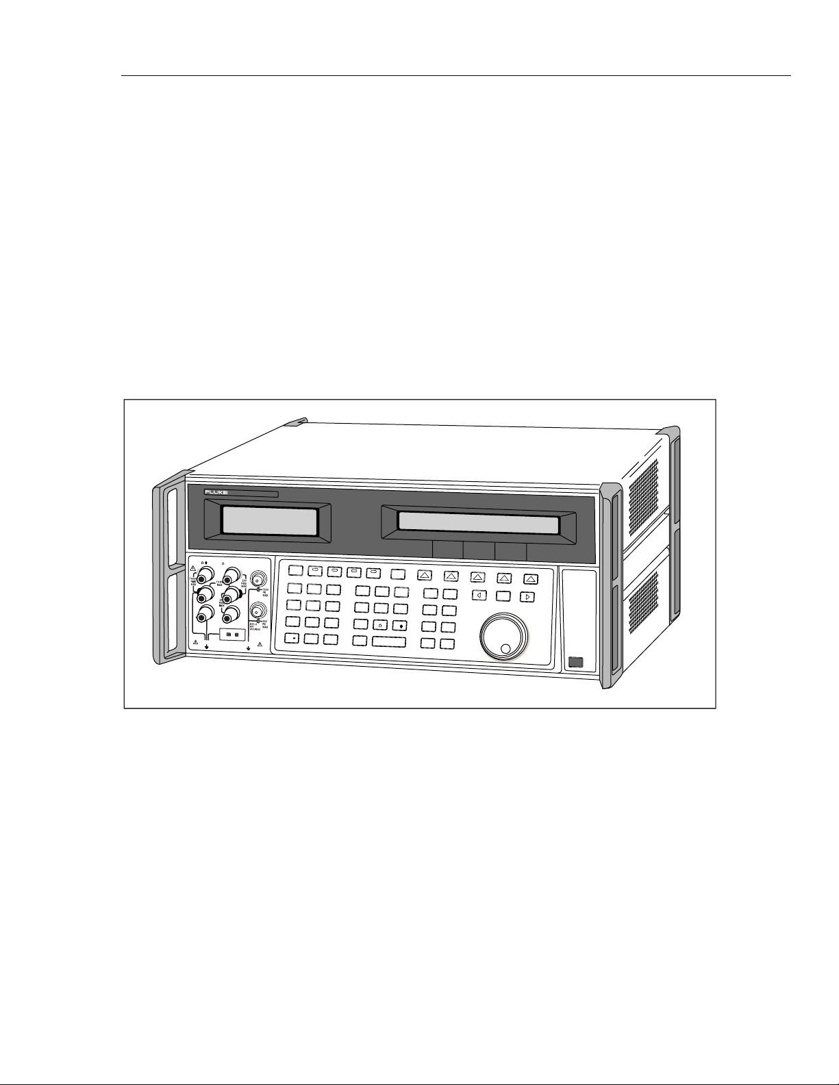
The Fluke Model 5520A Multi-Product Calibrator (Figure 1-1) is a precise instrument
that calibrates a wide variety of electrical measuring instruments. With the 5520A
Calibrator, you can calibrate precision multimeters that measure ac or dc voltage, ac or dc
current, ac or dc power, resistance, capacitance, and temperature. The 5520A can display
pressure measurements when used with a Fluke 700 Series Pressure Module. With the
SC600 and SC300 Oscilloscope Calibration options, you can use the 5520A Calibrator to
calibrate analog and digital oscilloscopes. Specifications are provided in this chapter
(specifications for the oscilloscope calibration options are provided in Chapter 6).
If the 5520A Calibrator is operated in any way not specified by
this manual or other documentation provided by Fluke, the
protection provided by the Calibrator may be impaired.
XWWarning
Introduction and Specifications
Introduction
1
NORMAL AUX
V, , ,
RTD
A, -SENSE,
HI
LO
GUARD
20V PK MAX
5520A
TC
AUX V
20A
20V PK MAX
CALIBRATOR
SCOPE
OUT
TRIG
p
SHIFT
µ
n
M
SCOPE
m
k
PREV
MENU
dBm sec
VHz
W
¡F
A
¡C
F
ENTER
SETUP
RESET
NEW
CE
REF
MEAS
MORE
TC
MODES
MULT
DIV
x
÷
EDIT
FIELD
OPRSTBY EARTH
789
456
123
+
/
0•
EXGRD
Figure 1-1. 5520A Multi-Product Calibrator
POWER
yg030f.eps
1-3
Page 20

5520A
Service Manual
1-2. Operation Overview
1-3. Local Operation
1-4. Remote Operation (RS-232)
The 5520A Calibrator may be operated at the front panel in the local mode, or remotely
using RS-232 or IEEE-488 ports. For remote operations, several software options are
available to integrate 5520A operation into a wide variety of calibration requirements.
Typical local operations include front panel connections to the Unit Under Test (UUT),
and then manual keystroke entries at the front panel to place the calibrator in the desired
output mode. The front panel layout facilitates hand movements from left to right, and
multiply and divide keys make it easy to step up or down at the press of a single key. You
can also review 5520A Calibrator specifications at the push of two keys.
There are two rear-panel serial data RS-232 ports: SERIAL 1 FROM HOST, and
SERIAL 2 TO UUT (Figure 1-2). Each port is dedicated to serial data communications
for operating and controlling the 5520A during calibration procedures. For complete
information on remote operation, see Chapter 5 of the 5520A Operators Manual.
The SERIAL 1 FROM HOST serial data port connects a host terminal or personal
computer to the 5520A. You have several choices for sending commands to the 5520A:
you can enter commands from a terminal (or a PC running a terminal program), you can
write your own programs using BASIC, or you can run optional Windows-based software
such as 5500/CAL or MET/CAL. The 5500/CAL software includes more than 200
example procedures covering a wide range of test tools the 5520A can calibrate.
The SERIAL 2 TO UUT serial data port connects a UUT to a PC or terminal via the
5520A (see Figure 1-3). This “pass-through” configuration eliminates the requirement for
two COM ports at the PC or terminal. A set of four commands control the operation of
the SERIAL 2 TO UUT serial port. See Chapter 6 of the 5520A Operators Manual for a
discussion of the UUT_* commands. The SERIAL 2 TO UUT port is also used to
connect to the Fluke 700 series pressure modules.
1-5. Remote Operation (IEEE-488)
The 5520A rear panel IEEE-488 port is a fully programmable parallel interface bus
meeting standard IEEE-488.1 and supplemental standard IEEE-488.2. Under the remote
control of an instrument controller, the 5520A Calibrator operates exclusively as a
“talker/listener.” You can write your own programs using the IEEE-488 command set or
run the optional Windows-based MET/CAL software. (See the 5520A Operators Manual
for a discussion of the general commands available for IEEE-488 operation, and
Chapter 3 of this manual for remote commands used for 5520A calibration.)
1-4
Page 21
Introduction and Specifications
Service Information
1
5520A
SERIAL 2
TO UUT port
SERIAL 1 FROM HOST port
RS-232 Remote Operation using the
SERIAL 1 FROM HOST port
SERIAL 1 FROM HOST port
5520A
RS-232 Remote Operation using the
SERIAL 1 FROM HOST and
SERIAL 2 TO UUT ports
COM port
PC or Terminal
COM port
PC or Terminal
Unit Under Test
Figure 1-2. RS-232 Remote Connections
1-6. Service Information
In case of difficulty within the 1-year Warranty period, return the Calibrator to a Fluke
Service Center for Warranty repair. For out of Warranty repair, contact a Fluke Service
Center for a cost estimate.
This service manual provides instructions for verification of performance, calibration,
and maintenance. If you choose to repair a malfunction, information in this manual can
help you to determine which module (printed circuit assembly) has a fault.
1-7. How to Contact Fluke
To contact Fluke, call one of the following telephone numbers:
• 1-888-99FLUKE (1-888-993-5853) in U.S.A.
• 1-800-36-FLUKE (1-800-363-5853) in Canada
• +31-402-678-200 in Europe
• +81-3-3434-0181 Japan
• +65-738-5655 Singapore
• +1-425-446-5500 from other countries
Or, visit Fluke’s Web site at www.fluke.com.
nn031f.eps
1-5
Page 22
5520A
Service Manual
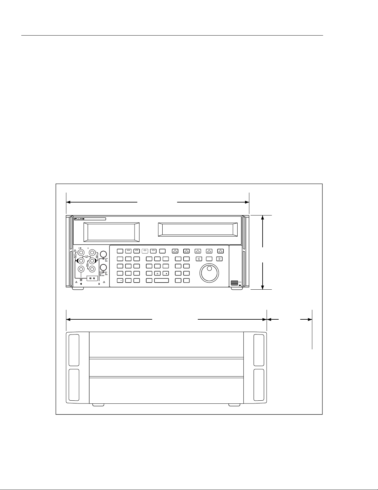
1-8. Specifications
The following tables list the 5520A specifications. All specifications are valid after
allowing a warm-up period of 30 minutes, or twice the time the 5520A has been turned
off. (For example, if the 5520A has been turned off for 5 minutes, the warm-up period is
10 minutes.)
All specifications apply for the temperature and time period indicated. For temperatures
outside of t
±5 °C (t
cal
is the ambient temperature when the 5520A was calibrated), the
cal
temperature coefficient as stated in the General Specifications must be applied.
The specifications also assume the Calibrator is zeroed every seven days or whenever the
ambient temperature changes more than 5 °C. The tightest ohms specifications are
maintained with a zero cal every 12 hours within ±1 °C of use.
Also see additional specifications later in this chapter for information on extended
specifications for ac voltage and current. The dimensional outline for the 5520A
Calibrator is shown in Figure 1-3.
43.2 cm (17 in)
5520A CALIBRATOR
NORMAL AUX
V, , ,
RTD
A, -SENSE,
HI
LO
GUARD
20V PK MAX
SCOPE
AUX V
OUT
STBY
OPR EARTH EXGRD SCOPE MENU
789
TRIG
456
20A
20V PK MAX
TC
123
+
0•
/
µ
m
n
k
p
M
SHIFT
PREV
dBm sec
VHz
W
¡F
¡CA
F
ENTER
SETUP
NEW
REF
MEAS
TC
MULTxDIV
RESET
MORE
MODES
EDIT
FIELD
CE
÷
POWER
(7 in)
I
O
17.8 cm
47.0 cm (18.5 in) 6.4 cm
(2.5 in)
For Cable
Access
1-6
nn032f.eps
Figure 1-3. 5520A Calibrator Dimensional Outline
Page 23
Introduction and Specifications
1-9. General Specifications
Warmup Time Twice the time since last warmed up, to a maximum of 30 minutes.
Settling Time Less than 5 seconds for all functions and ranges except as noted.
Standard Interfaces IEEE-488 (GPIB), RS-232, 5725A Amplifier
Temperature Performance • Operating: 0 °C to 50 °C
• Calibration (tcal): 15 °C to 35 °C
• Storage: -20 °C to 70 °C [3]
Temperature Coefficient Temperature Coefficient for temperatures outsi de tc al +5 °C is 0.1X/°C of
the 90-day specification (or 1-year, as applicable) per ° C.
Relative Humidity [1] • Operating: <80% to 30 °C, <70% to 40 °C, <40% to 50 °C
• Storage: <95%, non-condensing
Altitude • Operating: 3,050 m (10,000 ft) maximum
Safety Complies with IEC 1010-1 (1992-1); ANSI/ISA-S 82.01-1994;
Analog Low Isolation 20 V
EMC Designed to comply with FCC Rules Part 15; VFG 243/1991. If used in
Line Power [2] • Line Voltage (selectable): 100 V, 120 V, 220 V, 240 V
Power Consumption 5500A Calib rat o r, 300 VA; 5725A Ampl i fi er, 750 VA
Dimensions 5500A Calibrator:
Weight (without options) 5500A Calibrator, 22 kg (49 lb); 5725A Amplifier 32 kg (70 pounds)
Absolute Uncertainty Definition The 5500A specifications include stability, temperature coefficient, lineari ty,
Specification Confidence
Interval
• Non-operating: 12,200 m (40,000 ft) maximum
CAN/CSA-C22.2 No. 1010.1-92
areas with Electromagnetic fields of 1 to 3 V/m, resistance outputs have a
floor adder of 0.508 •. Performance not specified above 3 V/m. This
instrument may be susceptible to electro-stat ic disc harge (ES D) f rom direct
contact to the binding posts. Good static aware practices should be
followed when handling this and other pieces of electronic equipment.
• Line Frequency: 47 Hz to 63 Hz
• Line Voltage Variation: ±10% about line voltage setting
• Height: 17.8 cm (7 inches), standard rack increment, plus 1.5 cm (0.6
inch) for feet on bottom of unit;
• Width: 43.2 cm (17 inches), standard rack width
• Depth: 47.3 cm (18.6 inches) overall 5725A Amplifier:
• Height, 13.3 cm (5.25 inches), standard rack increment, plus 1.5 cm (0.6
inch) for feet on bottom of unit;
• Width, 43.2 cm (17 inches), standard rack width
• Depth, 63.0 cm (24.8 inches) overall.
line and load regulation, and the traceability of the external standards used
for calibration. You do not need to add anything to determine the total
specification of the 5520A for the temperature range indicated.
99%
Specifications
1
[1] After long periods of storage at high humidity, a drying out period (with the power on) of at least one week may be
required.
[2] For optimal performance at full dual outputs (e.g. 1000 V, 20A) choose a line voltage sett i ng that is ± 7.5% from
nominal.
[3] The DC Current ranges 0 to 1.09999 A and 1.1 A to 2.99999 A are sensitive to storage temperatures above 50 °C.
If the 5520A is stored above 50 °C for greater than 30 minutes, these ranges must be re-calibrated. Otherwi se, the
90 day and 1 year uncertainties of these ranges double.
1-7
Page 24
5520A
Service Manual
1-10. DC Volt age Specifi cati ons
Absolute Uncertainty, tcal
± 5 °C
± (ppm of output + µV)
Range 90 days 1 year
0 to 329.9999 mV 15 + 1 20 + 13 + 1 0.1 50 Ω
0 to 3.299999 V 9 + 2 11 + 22 + 1.5 1 10 mA
0 to 32.99999 V 10 + 20 12 + 20 2 + 15 10 10 mA
30 V to 329.9999 V 15 + 150 18 + 150 2 .5 + 100 100 5 mA
100 V to 1000.000 V 15 + 1500 18 + 1500 3 + 300 1000 5 mA
Auxiliary Output (dual output mode only) [2]
0 to 329.999 mV 300 + 350 400 + 350 30 + 100 1 5 mA
0.33V to 3.29999V 300 + 350 400 + 350 30 + 100 10 5 mA
3.3 V to 7 V 300 + 350 400 + 350 30 + 100 100 5 mA
TC Simulate and Measure in Linear 10 µV/°C and 1 mV/°C modes [3]
0 to 329.999 mV 40 + 3 50 + 35 + 2 0.1 10 Ω
[1] Remote sensing is not provided. Output resistance is < 5 mΩ for outputs ≥ 0.33 V. The AUX output
has an output resistance of < 1Ω. TC simulation has an output impedance of 10 Ω ± 1 Ω.
Stability
24 hours, ± 1 °C
± (ppm output + µV)
Resolution
µV[1]
Max
Burden
[2] Two channels of dc voltage output are provided.
[3] TC simulating and measuring are not specified for operation in electromagnetic fields above 0.4 V/m.
Noise
Range
0 to 329.9999 mV 0 + 1 µV6 µV
0 to 3.299999 V 0 + 10 µV 60 µV
0 to 32.99999 V 0 + 100 µV 600 µV
30 to 329.9999 V 10 + 1 mV 20 mV
100 to 1000.000 V 10 + 5 mV 20 mV
0 to 329.999 mV 0 + 5 µV 20 µV
0.33 V to
3.29.999 V
3.3 V to 7 V 0 + 100 µV 1000 µV
[1] Two channels of dc voltage output are provided.
Bandwidth 0.1 Hz to
10 Hz p-p
± (ppm output + floor)
Auxiliary Output (dual output mode only) [1]
0 + 20 µV 200 µV
Bandwidth 10 Hz to 10 kHz
rms
1-8
Page 25
1-11. DC Current Specifi cations
Introduction and Specifications
Specifications
1
Absolute Uncertainty,
tcal ± 5 °C
± (ppm of output + µA)
Range
0 to 329.999 mA 120 + 0.02 150 + 0.02 1 nA 10
0 to 3.29999 mA 80 + 0.05 100 + 0.05 0.01 mA 10
0 to 32.9999 mA 80 + 0.25 100 + 0.25 0.1 mA 7
0 to 329.999 mA 80 + 2.5 100 + 2.5 1 mA 7 400
0 to 1.09999 A 160 + 40 200 + 40 10 mA 6
1.1 to 2.99999 A 300 + 40 380 + 40 10 mA 6
0 to 10.9999 A
(20 A Range) 380 + 500 500 + 500 100 mA 4
11 to 20.5 A [1] 800 + 750 [2] 1000 + 750
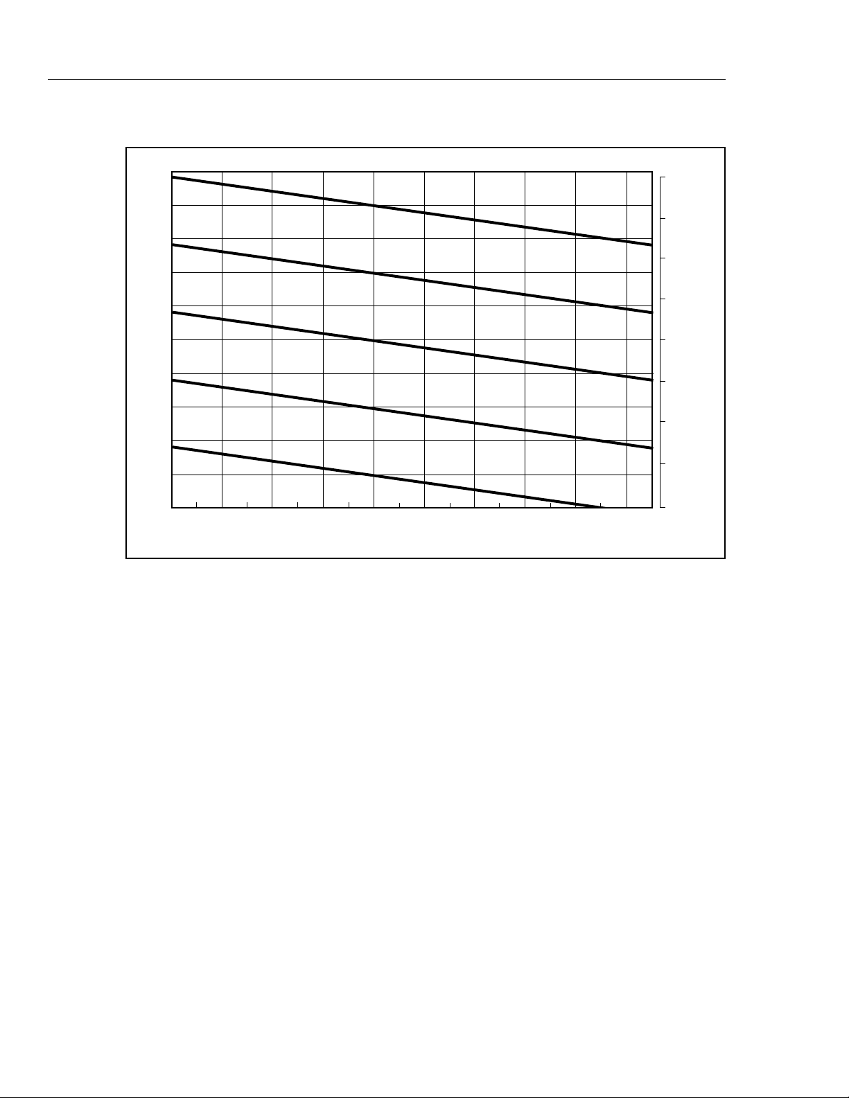
[1] Duty Cycle: Currents < 11 A may be provided continuously. For currents >11 A, see Figure 1-4. The current may be
provided 60-T-I minutes any 60 minute period where T is the temperature in °C (room temperature is about 23 °C)
and I is the output current in amperes. For example, 17 A, at 23 °C could be provided for 60-17-23 = 20 minutes
each hour.
90 days 1 year
[2]
Resolution
100 mA 4
Max
Compliance
Voltage
V
Max
Inductive
Load
mH
[2] Floor specification is 1500 µA within 30 seconds of selecting operate. For operating times > 30 seconds, the floor
specification is 750 µA.
Noise
Bandwidth
10 Hz to 10 kHz
rms
Range
Bandwidth
0.1 Hz to 10 Hz
p-p
0 to 329.999 µA 2 nA 20 nA
0 to 3.29999 mA 20 nA 200 nA
0 to 32.9999 mA 200 nA 2.0 µA
0 to 329.999 mA 2000 nA 20 µA
0 to 2.99999 A 20 µA1 mA
0 to 20.5 A 200 µA 10 mA
1-9
Page 26
5520A
Service Manual
DC Current Specifications (cont)
50
45
40
35
10 °C
30
25
Minutes per Hour
20
15
10
5
0
11 12 13 14 15 16 17 18 19 20
40 °C
30 °C
Current (Amps)
20 °C
Ambient
Figure 1-4. Allowable Duration of Current > 11 A
0 °C
80%
70%
60%
50%
40%
Duty Cycle (%)
30%
20%
10%
0%
nn326f.eps
1-10
Page 27
1-12. Resistance Specifications
Introduction and Specifications
Specifications
1
Range
[1]
0 to
10.9999 Ω
11 Ω to
32.9999 Ω
33 Ω to
109.9999 Ω
110 Ω to
329.9999 Ω
330 Ω to
1.099999 kΩ
1.1 kΩ to
3.299999 kΩ
3.3 kΩ to
10.99999 kΩ
11 kΩ to
32.99999 kΩ
33 kΩ to
109.9999 kΩ
110 kΩ to
329.9999 kΩ
330 kΩ to
1.099999 MΩ
1.1 MΩ to
3.299999 MΩ
3.3 MΩ to
10.99999 MΩ
11 MΩ to
32.99999 MΩ
33 MΩ to
109.9999 MΩ
110 MΩ to
329.9999 MΩ
330 MΩ to
1100 MΩ
[1] Continuously variable from 0 Ω to 1.1 G Ω.
[2] Applies for a 4-WIRE compensation only. For 2-WIRE and 2-WIRE COMP, add 5 µV per Amp of stimulus current
to the floor specification. For example, in 2-WIRE mode, at 1 ke, the floor specification within 12 hours of an ohms
zero cal for a measurement current of 1 mA is:
0.002 e + 5 µV/1 ma = (0.002 + 0.005) e = 0.007
[3] For currents lower than shown, the floor adder increases by:
Floor (new) = Floor (old) XImin/Iactual.
For example, a 50 µA stimulus measuring 100 e, has a floor specification of: 0.0014 e X 1 mA/50 µA = 0.028 e,
assuming an ohms zero cal within 12 hours.
ppm of output
90 days 1 year 12 hrs ± 1 °C 7 days ± 5 °C
110 130 50 250 10 250 nA to 1.8 µA
200 250 2500 2500 10 25 nA to 500 nA
400 500 3000 3000 100 25 nA to 180 nA
2500 3000 100000 100000 1000 2.5 nA to 50 nA
12000 15000 500000 500000 10000 1 nA to 13 nA
Absolute Uncertainty, tcal ± 5 °C
± (ppm of output + floor) [2]
Floor
Time & temp since ohms zero
cal
35 40 0.001 0. 01 0.0001 1 mA to 125 mA
25 30 0.0015 0.015 0.0001 1 mA to 125 mA
22 28 0.0014 0.015 0.0001 1 mA to 70 mA
22 28 0.002 0.02 0.0001 1 mA to 40 mA
22 28 0.002 0.02 0.001 1 mA to 18 mA
22 28 0.02 0.2 0.001 100 µA to 5 mA
22 28 0.02 0.1 0.01 100 µA to 1.8 mA
22 28 0.2 1 0.01 10 µA to 0.5 mA
22 28 0.2 1 0. 1 10 µA to 0.18 mA
25 32 2 10 0.1 1 µA to 0.05 mA
25 32 2 10 1 1 µA to 0.018 mA
40 60 30 150 1 250 nA to 5 µA
e
Resolution Allowable
Ω Current [3]
1-11
Page 28
5520A
Service Manual
1-13. AC Voltage (Sine Wave) Specifications
NORMAL (Normal Output)
Absolute Uncertainty,
Range Frequency
1.0 mV to 10 Hz to 45 Hz 600 + 6 800 + 61 µV 50 Ω
32.999 mV 45 Hz to 10 kHz 120 + 6 150 + 6 0.035 + 90 µV
10 kHz to 20 kHz 160 + 6 200 + 6 0.06 + 90 µV
20 kHz to 50 kHz 800 + 6 1000 + 6 0.15 + 90 µV
50 kHz to 100 kHz 3000 + 12 3500 + 12 0.25 + 90 µV
100 kHz to
500 kHz
33 mV to 10 Hz to 45 Hz 250 + 8 300 + 81 µV 50 Ω
329.999 mV 45 Hz to 10 kHz 140 + 8 145 + 8 0.035 + 90 µV
10 kHz to 20 kHz 150 + 8 160 + 8 0.06 + 90 µV
20 kHz to 50 kHz 300 + 8 350 + 8 0.15 + 90 µV
50 kHz to 100 kHz 600 + 32 800 + 32 0.20 + 90 µV
100 kHz to
500 kHz
0.33 V to 10 Hz to 45 Hz 250 + 50 300 + 50 10 µV 10 mA
3.29999 V 45 Hz to 10 kHz 140 + 60 150 + 60 0.035 + 200 µV
10 kHz to 20 kHz 160 + 60 190 + 60 0.06 + 200 µV
20 kHz to 50 kHz 250 + 50 300 + 50 0.15 + 200 µV
50 kHz to 100 kHz 550 + 125 700 + 125 0.20 + 200 µV
100 kHz to
500 kHz
3.3 V to 10 Hz to 45 Hz 250 + 650 300 + 650 100 µV 10 mA
32.9999 V 45 Hz to 10 kHz 125 + 600 150 + 600 0.035 + 2 mV
10 kHz to 20 kHz 220 + 600 240 + 600 0.08 + 2 mV
20 kHz to 50 kHz 300 + 600 350 + 600 0.2 + 2 mV
50 kHz to 100 kHz 750 + 1600 900 + 1600 0.5 + 2 mV
33 V to 45 Hz to 1 kHz 150 + 2000 190 + 2000 1 mV 5 mA,
329.999 V 1 kHz to 10 kHz 160 + 6000 200 + 6000 except 0.05 + 10 mV
10 kHz to 20 kHz 220 + 6000 250 + 6000 20 mA for 0.6 + 10 mV
20 kHz to 50 kHz 240 + 6000 300 + 6000 45 Hz to 0.8 + 10 mV
50 kHz to 100 kHz 1600 +
330 V to
1020 V
[1] Max Distortion for 100 kHz to 200 kHz. For 200 kHz to 500 kHz, the maximum distortion is 0.9% of
output + floor as shown.
Note
• Remote sensing is not provided. Output resistance is < 5 mΩ for outputs ≥0.33 V. The AUX output
resistance is < 1Ω. The maximum load capacitance is 500 pF, subject to the maximum burden current
limits.
45 Hz to 1 kHz 250 + 10000 300 +
1 kHz to 5 kHz 200 + 10000
5 kHz to 10 kHz 250 + 10000 300 +
6000 + 50 8000 + 50 0.3 + 90 µV [1]
1600 + 70 2000 + 70 0.20 + 90 µV [1]
2000 + 600 2400 + 600 0.20 + 200 µV [1]
50000
tcal ± 5 °C
± (ppm of output + µV)
90 days 1 year
2000 +
50000
10000
250 +
10000
10000
Resolution
10 mV 2 mA,
Max
Burden
65 Hz 1.0 + 10 mV
except
6 mA for
45 Hz to
65 Hz 0.07 + 30 mV
Max Distortion
and Noise
10 Hz to 5 MHz
Bandwidth
± (% output +
floor)
0.15 + 90 µV
0.15 + 90 µV
0.15 + 200 µV
0.15 + 2 mV
0.15 + 10 mV
0.15 + 30 mV
0.07 + 30 mV
1-12
Page 29
AC Voltage (Sine Wave) Specifications (cont)
AUX (Auxiliary Output) [dual output mode only] [1]
Introduction and Specifications
Specifications
1
Absolute Uncertainty,
Range Frequency
10 mV to 10 Hz to 20 Hz 0.15 + 370 0.2 + 370 1 µV5 mA
329.999 mV 20 Hz to 45 Hz 0.08 + 370 0.1 + 370 0.06 + 200 µV
45 Hz to 1 kHz 0.08 + 370 0.1 + 370 0.08 + 200 µV
1 kHz to 5 kHz 0.15 + 450 0.2 + 450 0.3 + 200 µV
5 kHz to 10 kHz 0.3 + 450 0.4 + 450 0.6 + 200 µV
10 Hz to 30 kHz 4.0 + 900 5.0 + 900 1 + 200 µV
0.33 V to 10 Hz to 20 Hz 0.15 + 450 0.2 + 450 10 µV5 mA
3.29999 V 20 Hz to 45 Hz 0.08 + 450 0.1 + 450 0.06 + 200 µV
45 Hz to 1 kHz 0.07 + 450 0.09 +
1 kHz to 5 kHz 0.15 + 1400 0.2 +
5 kHz to 10 kHz 0.3 + 1400 0.4 +
10 kHz to 30 kHz 4.0 + 2800 5.0 +
3.3 V to 5 V 10 Hz to 20 Hz 0.15 + 450 0.2 + 450 100 µV5 mA
20 Hz to 45 Hz 0.08 + 450 0.1 + 450 0.06 + 200 µV
45 Hz to 1 kHz 0.07 + 450 0.09 +
1 kHz to 5 kHz 0.15 + 1400 0.2 +
5 kHz to 10 kHz 0.3 +1400 0.4 +
tcal ± 5 °C
± (% of output + µV)
90 days 1 year
450
1400
1400
2800
450
1400
1400
Resolution
Max
Burden
Max Distortion
and Noise
10 Hz to
100 kHz
Bandwidth
± (% output +
floor)
0.2 + 200 µV
0.2 + 200 µV
0.08 + 200 µV
0.3 + 200 µV
0.6 + 200 µV
1 + 200 µV
0.2 + 200 µV
0.08 + 200 µV
0.3 + 200 µV
0.6 + 200 µV
[1] There are two channels of voltage output. The maximum frequency of the dual output is 30 kHz.
Note
• Remote sensing is not provided. Output resistance is < 5 mΩ for outputs ≥0.33 V. The AUX output
resistance is < 1Ω. The maximum load capacitance is 500 pF, subject to the maximum burden
current
limits.
1-13
Page 30
5520A
y
Service Manual
1-14. AC Current (Sine Wave) Specifications
LCOMP off
Max
Distortion &
Range Frequency
29.00 µA to 10 Hz to 20 Hz 0.16 + 0.1 0.2 + 0.1 0.05 0.15 + 0.5 µA 200
329.99 µA 20 Hz to 45 Hz 0.12 + 0.1 0.15 + 0.1 0.05 0.1 + 0.5 µA
45 Hz to 1 kHz 0.1 + 0.1 0.125 + 0.1 0.05 0.05 + 0.5 µA
1 kHz to 5 kHz 0.25 + 0.15 0.3 + 0.15 1.5 0.5 + 0.5 µA
5 kHz to 10 kHz 0.6 + 0.2 0.8 + 0.2 1.5 1.0 + 0.5 µA
10 kHz to 30
kHz
0.33 mA to 10 Hz to 20 Hz 0.16 + 0.15 0.2 + 0.15 0.05 0.15 + 1.5 µA 200
3.2999 mA 20 Hz to 45 Hz 0.1 + 0.15 0.125 + 0.15 0.05 0.06 + 1.5 µA
45 Hz to 1 kHz 0.08 + 0.15 0.1+ 0.15 0.05 0.02 + 1.5 µA
1 kHz to 5 kHz 0.16 + 0.2 0.2 + 0.2 1.5 0.5 + 1.5 µA
5 kHz to 10 kHz 0.4 + 0.3 0.5 + 0.3 1.5 1.0 + 1.5 µA
10 kHz to 30
kHz
3.3 mA to 10 Hz to 20 Hz 0.15 + 2 0.18 + 2 0.05 0.15 + 5 µA50
32.999 mA 20 Hz to 45 Hz 0.075 + 2 0.09 + 2 0.05 0.05 + 5 µA
45 Hz to 1 kHz 0.035 + 2 0.04 + 2 0.05 0.07 + 5 µA
1 kHz to 5 kHz 0.065 + 2 0.08 + 2 1.5 0.3 + 5 µA
5 kHz to 10 kHz 0.16 + 3 0.2 + 3 1.5 0.7 + 5 µA
10 kHz to 30
kHz
33 mA to 10 Hz to 20 Hz 0.15 +20 0.18 + 20 0.05 0.15 + 50 µA50
329.99 mA 20 Hz to 45 Hz 0.075 + 20 0.09 + 20 0.05 0.05 + 50 µA
45 Hz to 1 kHz 0.035 + 20 0.04 + 20 0.05 0.02 + 50 µA
1 kHz to 5 kHz 0.08 + 50 0.10 + 50 1.5 0.03 + 50 µA
5 kHz to 10 kHz 0.16 + 100 0.2 + 100 1.5 0.1 + 50 µA
10 kHz to 30
kHz
0.33 A to 10 Hz to 45 Hz 0.15 + 100 0.18 + 100 0.2 + 500 µA2.5
1.09999 A 45 Hz to 1 kHz 0.036 + 100 0.05 + 100 0.07 + 500 µA
1 kHz to 5 kHz 0.5 + 1000 0.6 + 1000 [3] 1 + 500 µA
5 kHz to 10 kHz 2.0 + 5000 2.5 + 5000 [4] 2 + 500 µA
1.1 A to 10 Hz to 45 Hz 0.15 + 100 0.18 + 100 0.2 + 500 µA2.5
2.99999 A 45 Hz to 1 kHz 0.05 + 100 0.06 + 100 0.07 + 500 µA
1 kHz to 5 kHz 0.5 + 1000 0.6 + 1000 [3] 1 + 500 µA
5 kHz to 10 kHz 2.0 + 5000 2.5 + 5000 [4] 2 + 500 µA
3 A to 45 Hz to 100 Hz 0.05 + 2000 0.06 + 2000 0.2 + 3 mA 1
10.9999 A
11A to 45 Hz to 100 Hz 0.1 + 5000 0.12 + 5000 0.2 + 3 mA 1
20.5 A 100 Hz to 1 kHz 0.13 + 5000 0.15 + 5000 0.1 + 3 mA
[2] 1 kHz to 5 kHz 2.5 + 5000 3.0 + 5000 0.8 + 3 mA
[1] Max Distortion for 100 kHz to 200 kHz. For 200 kHz to 500 kHz, the maximum distortion is 0.9% of
output + floor as shown.
[2] Duty Cycle: Currents < 11 A may be provided continuously. For currents > 11 A, see Figure 1-4. The
current ma
temperature is about 23°C) and I is the output current in Amps. For example, 17 A, at 23°C could be
provided for 60-17-23 = 20 minutes each hour.
[3] For compliance voltages greater than 1 V, add 1 mA/V to the floor specification from 1 kHz to 5 kHz.
[4] For compliance voltages greater than 1 V, add 5 mA/V to the floor specification from 5 kHz to 10 kHz.
100 kHz to 1
kHz
1 kHz to 5 kHz 2.5 + 2000 3.0 + 2000 0.8 + 3 mA
be provided 60-T-I minutes any 60 minute period where T is the temperature in °C (room
Absolute Uncertainty,
tcal ± 5 °C
± (% of output + µA)
90 days 1 year floor) µH
1.2 + 0.4 1.6 + 0.4 10 1.2 + 0.5 µA
0.8 + 0.6 1.0 + 0.6 10 1.2 + 0.5 µA
0.32 + 4 0.4 + 4 10 1.0 + 0.5 µA
0.32 + 200 0.4 + 200 10 0.6 + 50 µA
0.08 + 2000 0.10 + 2000 0.1 + 3 mA
Compliance
adder
± (µA/V)
Noise 10 Hz
to 100 kHz
BW
± (% output
+
Max
Inductive
Load
1-14
Page 31

Introduction and Specifications
AC Current (Sine Wave) Specifications (cont)
LCOMP on
Absolute Uncertainty, tcal ± 5
Range Frequency
± (% of output + µA)
90 days 1 year
29.00 µA to 10 Hz to 100 Hz 0.2 + 0.2 0.25 + 0.2 0.1 + 1.0
329.99 µA 100 Hz to 1 kHz 0.5 + 0.5 0.6 + 0.5 0.05 + 1.0
0.33 mA to 10 Hz to 100 Hz 0.2 + 0.3 0.25 + 0.3 0.15 + 1.5
3.2999 mA 100 Hz to 1 kHz 0.5 + 0.8 0.6 + 0.8 0.06 + 1.5
3.3 mA to 10 Hz to 100 Hz 0.07 + 4 0.08 + 4 0.15 + 5 400
32.999 mA 100 Hz to 1 kHz 0.18 + 10 0.2 + 10 0.05 + 5
33 mA to 10 Hz to 100 Hz 0.07 + 40 0.08 + 40 0.15 + 50
329.99 mA 100 Hz to 1 kHz 0.18 + 100 0.2 + 100 0.05 + 50
°C
Max Distortion
& Noise, 10 Hz
to 100 kHz BW
± (% output +
µA)
Inductive
Specifications
Max
Load
µH
1
0.33 A to 10 Hz to 100 Hz 0.1 + 200 0.12 + 200 0.2 + 500
2.99999 A 100 to 440 Hz 0.25 + 1000 0.3 + 1000 0.25 + 500
3 A to 20.5 A 10 Hz to 100 Hz 0.1 + 2000 [2] 0.12 + 2000
[2]
[1] 100 Hz to 1 kHz 0.8 + 5000 [3] 1.0 + 5000 [3] 0.5 + 0
[1] Duty Cycle: Currents < 11 A may be provided continuously. For currents >11 A, see Figure 1-4. The
current may be provided 60-T-I minutes any 60 minute period where T is the temperature in °C (room
temperature is about 23 °C) and I is the output current in amperes. For example, 17 A, at 23 °C could
be provided for 60-17-23 = 20 minutes each hour.
[2] For currents >11 A, Floor specification is 4000 µA within 30 seconds of selecting operate. For
operating times >30 seconds, the floor specification is 2000 µA.
[3] For currents >11 A, Floor specification is 1000 µA within 30 seconds of selecting operate. For
operating times >30 seconds, the floor specification is 5000 µA.
[4] Subject to compliance voltages limits.
Range Resolution
µA
0.029 mA to 0.32999 mA 0.01 7
0.33 mA to 3.29999 mA 0.01 7
3.3 mA to 32.9999 mA 0.1 5
33 mA to 329.999 mA 1 5
0.33 A to 2.99999 A 10 4
3 A to 20.5 A 100 3
0.1 + 0 400 [4]
Max Compliance Voltage
V rms
[1] Subject to specification adder for compliance voltages greater than 1 V rms.
1-15
Page 32

5520A
Service Manual
1-15. Capacitance Specifications
Range
0.19 nF to
0.3999 nF
0.4 nF to
1.0999 nF
1.1 nF to
3.2999 nF
3.3 nF to
10.9999 nF
11 nF to
32.9999 nF
33 nF to
109.999 nF
110 nF to
329.999 nF
0.33 µF to
1.09999 µF
1.1 µF to
3.29999 µF
3.3 µF to
10.9999 µF
11 µF to
32.9999 µF
33 µF to
109.999 µF
110 µF to
329.999 µF
0.33 µF to
1.09999mF
1.1 mF to
3.2999 mF
3.3 mF to
10.9999 mF
11 mF to
32.9999 mF
33 mF to
110 mF
Notes:
Absolute Uncertainty, tcal
± 5 °C
± (% of output + floor)
Resolution
90 days 1 year
0.38 + 0.01 nF 0.5 + 0.01 nF 0.1 pF 10 Hz to 10 kHz 20 kHz 40 kHz
0.38 + 0.01 nF 0.5 + 0.01 nF 0.1 pF 10 Hz to 10 kHz 30 kHz 50 kHz
0.38 + 0.01 nF 0.5 + 0.01 nF 0.1 pF 10 Hz to 3 kHz 30 kHz 50 kHz
0.19 + 0.01 nF 0.25 + 0.01 nF 0.1 pF 10 Hz to 1 kHz 20 kHz 25 kHz
0.19 + 0.1 nF 0.25 + 0.1 nF 0.1 pF 10 Hz to 1 kHz 8 kHz 10 kHz
0.19 + 0.1 nF 0.25 + 0.1 nF 1 pF 10 Hz to 1 kHz 4 kHz 6 kHz
0.19 + 0.3 nF 0.25 + 0.3 nF 1 pF 10 Hz to 1 kHz 2.5 kHz 3.5 kHz
0.19 + 1 nF 0.25 + 1 nF 10 pF 10 Hz to 600 Hz 1.5 kHz 2 kHz
0.19 + 3 nF 0.25 + 3 nF 10 pF 10 Hz to 300 Hz 800 Hz 1 kHz
0.19 + 10 nF 0.25 + 10 nF 100 pF 10 Hz to 150 Hz 450 Hz 650 Hz
0.30 + 30 nF 0.40 + 30 nF 100 pF 10 Hz to 120 Hz 250 Hz 350 Hz
0.34 + 100 nF 0.45 + 100 nF 1 nF 10 Hz to 80 Hz 150 Hz 200 Hz
0.34 + 300 nF 0.45 + 300 nF 1 nF 0 to 50 Hz 80 Hz 120 Hz
0.34 + 1 µF 0.45 + 1 µF 10 nF 0 to 20 Hz 45 Hz 65 Hz
0.34 + 3 µF 0.45 + 3 µF 10 nF 0 to 6 Hz 30 Hz 40 Hz
0.34 + 10 µF 0.45 + 10 µF 100 nF 0 to 2 Hz 15 Hz 20 Hz
0.7 + 30 µF 0.75 + 30 µF 100 nF 0 to 0.6 Hz 7.5 Hz 10 Hz
1.0 + 100 µF1.1 + 100 µF 10 µF 0 to 0.2 Hz 3 Hz 5 Hz
Min and Max
Specification
Allowed Frequency or
Charge-Discharge Rate
Typical
to Meet
Max for
< 0.5%
Error
Typical
Max for
< 1%
Error
1-16
1. The output is continuously variable from 190 pF to 110 mF.
2. Specifications apply to both dc charge/discharge capacitance meters and ac RCL meters. The
maximum allowable peak voltage is 3 V. The maximum allowable peak current is 150 mA, with an rms
limitation of 30 mA below 1.1 µF and 100 mA for 1.1 µF and above.
3. The maximum lead resistance for no additional error in 2-wire COMP mode is 10 Ω.
Page 33

Introduction and Specifications
1-16. Temperature Calibration (Thermocouple) Specifications
Specifications
1
TC
Type
[1]
B 600 to 800 0.42 0.44 L -200 to -100 0.37 0.37
C 0 to 150 0.23 0.30 -100 to -25 0.17 0.22
E -250 to -100 0.38 0.50 250 to 400 0.28 0.35
Range
°C
[2]
800 to 1000 0.34 0.34 -100 to 800 0.26 0.26
1000 to 1550 0.30 0.30 800 to 900 0.17 0.17
1550 to 1820 0.26 0.33 N -200 to -100 0.30 0.40
150 to 650 0.19 0.26 -25 to 120 0.15 0.19
650 to 1000 0.23 0.31 120 to 410 0.14 0.18
1000 to 1800 0.38 0.50 410 to 1300 0.21 0.27
1800 to 2316 0.63 0.84 R 0 to 250 0.48 0.57
-100 to -25 0.12 0.16 400 to 1000 0.26 0.33
-25 to 350 0.10 0.14 1000 to 1767 0.30 0.40
Absolute Uncertainty
Source/Measure
tcal ±5 °C
± °C [3]
90 days 1 year 90 days 1 year
TC
Type
[1]
Range
°C
[2]
Absolute Uncertainty
Source/Measure
tcal ±5 °C
± °C [3]
350 to 650 0.12 0.16 S 0 to 250 0.47 0 .47
650 to 1000 0.16 0.21 250 to 1000 0.30 0.36
J -210 to -100 0.20 0.27 1000 to 1400 0.28 0.37
-100 to -30 0.12 0.16 1400 to 1767 0.34 0.46
-30 to 150 0.10 0.14 T -250 to -150 0.48 0.63
150 to 760 0.13 0.17 -150 to 0 0.18 0.24
760 to 1200 0.18 0.23 0 to 120 0 .12 0.16
K -200 to -100 0.25 0.33 120 to 400 0.10 0.14
-100 to -25 0.14 0.18 U -200 to 0 0.56 0.56
-25 to 120 0.12 0.16 0 to 600 0.27 0.27
120 to 1000 0.19 0.26
1000 to 1372 0.30 0.40
[1] Temperature standard ITS-90 or IPTS-68 is selectable.
TC simulating and measuring are not specified for operation in electromagnetic fields above 0.4 V/m.
[2] Resolution is 0.01 °C
[3] Does not include thermocouple error
1-17
Page 34

5520A
Service Manual
1-17. Temperature Calibration (RTD) Specifications
RTD
Type
Pt 395, -200 to -80 0.04 0.05 Pt 385, -200 to -80 0.03 0.04
100 Ω -80 to 0 0.05 0.05 500 Ω -80 to 0 0.04 0.05
Pt 3926, -200 to -80 0 .04 0.05 600 to 630 0.09 0.11
100 Ω -80 to 0 0.05 0.05 Pt 385, -200 to -80 0.03 0.03
Pt 3916, -200 to -190 0.25 0.25 300 to 400 0.05 0.07
100 Ω -190 to -80 0.04 0.04 400 to 600 0.06 0.07
Pt 385, -200 to -80 0.03 0.04
200 Ω -80 to 0 0.03 0.04
Range
°C
[1]
0 to 100 0.07 0.07 0 to 100 0.05 0.05
100 to 300 0.08 0.09 100 to 260 0.06 0.06
300 to 400 0.09 0.10 260 to 300 0.07 0.08
400 to 630 0.10 0.12 300 to 400 0.07 0.08
630 to 800 0.21 0.23 400 to 600 0.08 0.09
0 to 100 0.07 0.07 1000 Ω -80 to 0 0.03 0.03
100 to 300 0.08 0.09 0 to 100 0.03 0.04
300 to 400 0.09 0.10 100 to 260 0.04 0.05
400 to 630 0.10 0.12 260 to 300 0.05 0.06
-80 to 0 0.05 0.05 600 to 630 0.22 0.23
0 to 100 0.06 0.06 PtNi 385, -80 to 0 0.06 0.08
100 to 260 0.06 0.07 120 Ω 0 to 100 0.07 0.08
260 to 300 0.07 0.08 (Ni120) 100 to 260 0.13 0.14
300 to 400 0.08 0.09 Cu 427, -100 to 260 0.3 0.3
400 to 600 0.08 0.10 10 Ω [3]
600 to 630 0.21 0.23
0 to 100 0.04 0.04
100 to 260 0.04 0.05
260 to 300 0.11 0.12
300 to 400 0.12 0.13
400 to 600 0.12 0.14
600 to 630 0.14 0.16
Absolute
Uncertainty
tcal ±5 °C
± °C [2]
90 days 1 year 90 days 1 year
RTD
Type
Range
°C
[1]
Absolute
Uncertainty
tcal ±5 °C
± °C [2]
1-18
[1] Resolution is 0.003 °C
[2] Applies for COMP OFF (to the 5520A Calibrator front panel NORMAL terminals) and 2-wire and 4-
wire compensation.
[3] Based on MINCO Application Aid No. 18
Page 35

1-18. DC Power Specifi cati on Summary
Current Range
Introduction and Specifications
Specifications
1
Voltage Range
90 days 33 mV to 1020 V 0.021 0.019 [2] 0.06 [2]
1 year 33 mV to 1020 V 0.023 0.022 [2] 0.07 [2]
[1] To determine dc power uncertainty with more precision, see the individual “AC Voltage Spec if ications,” “AC
Current Specifications,” and “Calculating Power Uncertai nty.”
[2] Add 0.02% unless a settling time of 30 seconds is allowed for output currents > 10 A or for currents on the highest
two current ranges within 30 seconds of an output current > 10 A.
0.33 mA to
329.99 mA
Absolute Uncertainty, tcal ± 5 °C, ± (% of watts output) [1]
0.33 A to
2.9999 A
3 A to
20.5 A
1-19. AC Power (45 Hz to 65 Hz) Specification Summary, PF=1
Current Range
Voltage Range
90 days 33 to 329.999 mV 0.13 0.09 0.13 0.09
330 mV to 1020 V 0.11 0.07 0.11 0.07
1 year 33 to 329.999 mV 0.14 0.10 0.14 0.10
330 mV to 1020 V 0.12 0.08 0.12 0.08
3.3 mA to
8.999 mA
Absolute Uncertainty, tcal ± 5 °C, ± (% of watts output) [1]
9 mA to
32.999 mA
33 mA to
89.99 mA
90 mA
to 329.99 mA
Current Range [2]
Voltage Range
90 days 33 to 329.999 mV 0.12 0.10 0.12 0.10
330 mV to 1020 V 0.10 0.08 0.11 0.09
1 year 33 to 329.999 mV 0.13 0.11 0.13 0.11
330 mV to 1020 V 0.11 0.09 0.12 0.10
[1] To determine ac power uncertainty with more precision, see the individual “DC Volt age Specifications” and “DC
Current Specifications” and “Calculati ng Power Uncertainty.”
[2] Add 0.02% unless a settling time of 30 seconds is allowed for output currents > 10 A or for currents on the highest
two
current ranges within 30 seconds of an output current > 10 A.
0.33 A to
0.8999 A
Absolute Uncertainty, tcal ± 5 °C, ± (% of watts output) [1]
0.9 A to
2.1999 A
2.2 A to
4.4999 A
4.5 A to
20.5 A
1-19
Page 36

5520A
Service Manual
1-20. Power and Dual Output Limit Specificati ons
Frequency
dc 0 to ± 1020 V 0 to ± 20.5 A 0 to ± 7 V
10 Hz to 45 Hz 33 mV to 32.9999 V 3.3 mA to 2.99999 A 10 mV to 5 V 0 to 1
45 Hz to 65 Hz 33 mV to 1000 V 3.3 mA to 20.5 A 10 mV to 5 V 0 to 1
65 Hz to 500 Hz 330 mV to 1000 V 33 mA to 2.99999 A 100 mV to 5 V 0 to 1
65 Hz to 500 Hz 3.3 V to 1000 V 33 mA to 20.5 A 100 mV to 5 V 0 to 1
500 Hz to 1 kHz 330 mV to 1000 V 33 mA to 20.5 A 100 mV to 5 V 1
1 kHz to 5 kHz 3.3 V to 1000 V [1] 33 mA to 2.99999 A 100 mV to 5 V [1] 1
5 kHz to 10 kHz 3.3 V to 1000 V [2] 33 mA to 329.99 mA 1 V to 5 V [2] 1
[1] In dual voltage output mode, voltage is limited to 3.3 V to 500 V in the NORMAL output.
[2] In dual voltage output mode, voltage is limited to 3.3 V to 250 V in the NORMAL output.
Notes
The range of voltages and currents shown in “DC Voltage Specifications,” “DC Current Specifications,” “AC
Voltage (Sine Wave) Specifications,” and “AC Current (Sine Wave) Specifications” are available in the
power and dual output modes (except minimum current for ac power is 0.33 mA). However, only those
limits shown in this table are specified. See “Calculating Power Uncertainty” to determine the uncertainty at
these points.
Voltages
(NORMAL)
Currents
Voltages
(AUX)
Power
Factor
(PF)
The phase adjustment range for dual ac outputs is 0° to ± 179.99°. The phase resolution for dual ac
outputs is 0.01°.
1-20
Page 37

1-21. Phase Specifications
1-Year Absolute Uncertainty, tcal ± 5 °C, (∆ Φ °)
Introduction and Specifications
Specifications
1
10 Hz to
65 Hz
0.10° 0.25° 0.5° 2.5° 5° 10°
Phase
(Φ)
Watts
0° 90° 1.000 0.00% 0.00% 0.00% 0.10% 0.38% 1.52%
10° 80° 0.985 0.03% 0.08% 0.16% 0.86% 1.92% 4.58%
20° 70° 0.940 0.06% 0.16% 0.32% 1.68% 3.55% 7.84%
30° 60° 0.866 0.10% 0.25% 0.51% 2.61% 5.41% 11.54%
40° 50° 0.766 0.15% 0.37% 0.74% 3.76% 7.69% 16.09%
50° 40° 0.643 0.21% 0.52% 1.04% 5.29% 10.77% 22.21%
60° 30° 0.500 0.30% 0.76% 1.52% 7.65% 15.48% 31.60%
70° 20° 0.342 0.48% 1.20% 2.40% 12.08% 24.33% 49.23%
80° 10° 0.174 0.99% 2.48% 4.95% 24.83% 49.81% 100.00%
90° 0° 0.000
Phase
(Φ)
VARs
65 Hz to
500 Hz
PF
500 Hz to
10 Hz to
65 Hz
1 kHz to
1 kHz
Power Uncertainty Adder due to Phase Error
65 Hz to
500 Hz
5 kHz
500 Hz
to
1 kHz
5 kHz to
10 kHz
1 kHz
to
5 kHz
5 kHz
to
10 kHz
10 kHz to
30 kHz
10 kHz
to
30 kHz
Note
To calculate exact ac watts power adders due to phase uncertainty for
values not shown, use the following formula:
Cos
()
+
Adder
%(
=−
100 1
()
For example: for a PF of .9205 (
= 0.15, the ac watts power adder is:
∆Φ
Adder
%(
=−
()
Cos
Cos
Cos
Φ∆Φ
Φ
()
(23 )
+
15
.
23
()
) .
Φ
= 23) and a phase uncertainty of
=100 1
011%
).
1-21
Page 38

5520A
2
017
2
2
Service Manual
1-22. Calculati ng Power Uncertainty
Overall uncertainty for power output in watts (or VARs) is based on the root sum square
(rss) of the individual uncertainties in percent for the selected voltage, current, and power
factor parameters:
UUUU
Watts uncertainty
VARs uncertainty UUUU
power voltage current PFadder
VARs voltage current VARsadder
2
=++
2
=++
22
22
Because there are an infinite number of combinations, you should calculate the actual ac
power uncertainty for your selected parameters. The method of calculation is best shown
in the following examples (using 90-day specifications):
Example 1
Voltage Uncertainty Uncertainty for 100 V at 60 Hz is 150 ppm + 2 mV, totaling:
100 V x 190 x 10
Output: 100 V, 1 A, 60 Hz, Power Factor = 1.0 (Φ=0), 1 year specifications
-6
= 15 mV added to 2 mV = 17 mV. Expressed in percent:
17 mV/100 V x 100 = 0.017% (see “AC Voltage (Sine Wave) Specifications”).
Current Uncertainty Uncertainty for 1 A is 0.036% + 100 µA, totaling:
1 A x 0.00036 = 360 µA added to 100 µA = 0.46 mA. Expressed in percent:
0.46 mA/1 A x 100 = 0.046% (see “AC Current (Sine Waves) Specifications”).
PF Adder Watts Adder for PF = 1 (Φ=0) at 60 Hz is 0% (see “Phase Specifications”).
Total Watts Output Uncertainty = U
=++=0017 0 046 0 0 049%
power
2
.. .
22
Example 2 Output: 100 V, 1 A, 400 Hz, Power Factor = 0.5 (Φ=60)
Voltage Uncertainty Uncertainty for 100 V at 400 Hz is, 150 ppm + 2 mV, totaling:
100 V x 190 x 10
-6
= 15 mV added to 2 mV = 17 mV. Expressed in percent:
17 mV/100V x 100 = 0.017% (see “AC Voltage (Sine Wave) Specifications”).
Current Uncertainty Uncertainty for 1 A is 0.036% + 100 µA, totaling:
1 A x 0.00036 = 360 µA added to 100 µA = 0.46 mA. Expressed in percent:
0.46 mA/1A x 100 = 0.046% (see “AC Current (Sine Waves) Specifications”).
PF Adder Watts Adder for PF = 0.5 (Φ=60) at 400 Hz is 0.76% (see “Phase
Specifications”).
Total Watts Output Uncertainty =
U
=++=0017 0 046 076 076%
power
2
....
22
1-22
VARs When the Power Factor approaches 0.0, the watts output uncertainty becomes
unrealistic because the dominant characteristic is the VARs (volts-amps-reactive) output.
In these cases, calculate the Total VARs Output Uncertainty, as shown in example 3:
Example 3 Output: 100 V, 1 A, 60 Hz, Power Factor = 0.174 (Φ=80)
Voltage Uncertainty Uncertainty for 100 V at 400 Hz is, 150 ppm + 2 mV, totaling:
100 V x 190 x 10
-6
= 15 mV added to 2 mV = 17 mV. Expressed in percent:
17 mV/100V x 100 = 0.017% (see “AC Voltage (Sine Wave) Specifications”).
Current Uncertainty Uncertainty for 1 A is 0.036% + 100 µA, totaling:
1 A x 0.00036 = 360 µA added to 100 µA = 0.46 mA. Expressed in percent:
0.46 mA/1 A x 100 = 0.046% (see “AC Current (Sine Waves) Specifications”).
VARs Adder VARs Adder for Φ = 80 at 60 Hz is 0.02% (see “Phase Specifications”).
Total VARS Output Uncertainty = U
VARs =0
....++=
0046 0 03 0058%
Page 39

1-23. Additional Specifications
The following paragraphs provide additional specifications for the 5520A Calibrator ac
voltage and ac current functions. These specifications are valid after allowing a warm-up
period of 30 minutes, or twice the time the 5520A has been turned off. All extended
range specifications are based on performing the internal zero-cal function at weekly
intervals, or when the ambient temperature changes by more than 5 °C.
1-24. Frequency Specifications
Introduction and Specifications
Additional Specifications
1
Frequency
Range
0.01 Hz to 119.99 Hz 0.01 Hz
120.0 Hz to 1199.9 Hz 0.1 Hz
1.200 kHz to 11.999 kHz 1.0 Hz 2.5 ppm ± 5 µHz [1] 100 nS
12.00 kHz to 119.99 kHz 10 Hz
120.0 kHz to 1199.9 kHz 100 Hz
1.200 MHz to 2.000 MHz 1 kHz
[1] With REF CLK set to ext, the frequency uncertainty of the 5520A is the uncertainty of the external
10 MHz clock ± 5 µHz. The amplitude of the 10 MHz external reference clock signal should be
between 1 V and 5 V p-p.
Resolution
1-Year Absolute Uncertainty,
tcal ± 5°C
Jitter
1-23
Page 40

5520A
Service Manual
1-25. Harmonics (2nd to 50th) Specifications
Fundamental
Frequency [1]
10 Hz to 45 Hz 33 mV to 32.9999 V 3.3 mA to 2.99999 A 10 mV to 5 V Same % of
45 Hz to 65 Hz 33 mV to 1000 V 3.3 mA to 20.5 A 10 mV to 5 V the
65 Hz to 500 Hz 33 mV to 1000 V 33 mA to 20.5 A 100 mV to 5 V single output,
500 Hz to 5 kHz 330 mV to 1000 V 33 mA to 20.5 A 100 mV to 5 V floor adder.
5 kHz to 10 kHz 3.3 V to 1000 V 33 mA to
10 kHz to 30 kHz 3.3 V to 1000 V 33 mA to
[1] The maximum frequency of the harmonic output is 30 kHz (10 kHz for 3 V to 5 V). For example, if the
fundamental output is 5 kHz, the maximum selection is the 6th harmonic (30 kHz). All harmonic
frequencies (2nd to 50th) are available for fundamental outputs between 10 Hz and 600 Hz (200 Hz
for 3 V to 5 V).
Note
Voltages
NORMAL
Terminals
Currents
329.9999 mA
329.9999 mA
Voltages
AUX Terminals
100 mV to 5 V
100 mV to
3.29999 V
Amplitude
Uncertainty
output as
equivalent
but twice the
Phase uncertainty for harmonic outputs is 1°, or the phase uncertainty shown in “Phase Specifications”
for the particular output, whichever is greater. For example, the phase uncertainty of a 400 Hz
fundamental output and 10 kHz harmonic output is 10° (from “Phase Specifications”). Another
example, the phase uncertainty of a 60 Hz fundamental output and a 400 Hz harmonic output is 1°.
Example of determining Amplitude Uncertainty in a Dual Output Harmonic Mode
What are the amplitude uncertainties for the following dual outputs?
NORMAL (Fundamental) Output: 100V, 100 Hz
From “AC Voltage (Sine Wave) Specifications” the single output specification for
100V, 100 Hz, is 0.015% + 2 mV. For the dual output in this example, the specification
is 0.015% + 4 mV as the 0.015% is the same and the floor is twice the value (2 x 2 mV).
AUX (50th Harmonic) Output: 100 mV, 5 kHz
From “AC Voltage (Sine Wave) Specifications” the auxiliary output specification for
100 mV, 5 kHz, is 0.15% + 450 mV. For the dual output in this example, the specification
is 0.15% + 900 mV as the 0.15% is the same and the floor is twice the value (2 x 450 mV).
1-24
Page 41

Introduction and Specifications
1-26. AC Volt age (Sine Wave) Extended Bandwidth Specifications
Additional Specifications
1
1-Year Absolute
Range Frequency
Normal Channel (Single Output Mode)
1.0 mV to 33 mV 0.01 Hz to 9.99 Hz ± (5.0 % of output + Two digits, e.g., 25 mV
34 mV to 330 mV 0.5% of range) Three digits
0.4 V to 33 V Two digits
0.3 V to 3.3V 500.1 kHz to 1 MHz -10 dB at 1 MHz, typical Two digits
1.001 MHz to 2 MHz -31 dB at 2 MHz, typical
Auxiliary Output (Dual Output Mode)
10 mV to 330 mV 0.01 Hz to 9.99 Hz ± (5.0 % of output + Three digits
0.4 V to 5V 0.5% of range) Two digits
Uncertainty
tcal ± 5 °C
Max Voltage
Resolution
1-25
Page 42

5520A
Service Manual
1-27. AC Voltage (Non-Sine Wave) Specifications
Triangle Wave
&
Truncated
Sine
Range, p-p [1]
2.9 mV
to 93 V 10 Hz to 45 Hz 0.25 + 0.5
93 mV
to 14 V 10 Hz to 45 Hz 0.25 + 0.5 Six digits on
Frequency 1-Year Absolute Uncertainty,
tcal ± 5 °C,
± (% of output + % of range) [2]
Normal Channel (Single Output Mode)
0.01 Hz to 10 Hz 5.0 + 0.5 Two digits on
45 Hz to 1 kHz 0.25 + 0.25 Six digits on
1 kHz to 20 kHz 0.5 + 0.25 each range
20 kHz to 100 kHz
[3]
Auxiliary Output (Dual Output Mode)
0.01 Hz to 10 Hz 5.0 + 0.5 Two digits on
45 Hz to 1 kHz 0.25 + 0.25 each range
1 kHz to 10 kHz 5.0 + 0.5
5.0 + 0.5
Max Voltage
Resolution
each range
each range
[1] To convert p-p to rms for triangle wave, multiply the p-p value by 0.2886751. To convert p-p to rms for
truncated sine wave, multiply the p-p value by 0.2165063.
[2] Uncertainty is stated in p-p. Amplitude is verified using an rms-responding DMM.
[3] Uncertainty for Truncated Sine outputs is typical over this frequency band.
Square
Wave Range
(p-p) [1]
2.9 mV 10 Hz to 45 Hz 0.25 + 0.5
to 45 Hz to 1 kHz 0.25 + 0.25 Six digits on each range
66 V 1 kHz to 20 kHz 0.5 + 0.25
66 mV 0.01 Hz to 10 Hz 5.0 + 0.5 Two digits on each range
to 10 Hz to 45 Hz 0.25 + 0.5
14V 45 Hz to 1 kHz 0.25 + 0.25 Six digits on each range
[1] To convert p-p to rms for square wave, multiply the p-p value by 0.5.
[2] Uncertainty is stated in p-p. Amplitude is verified using an rms-responding DMM.
[3] Limited to 1 kHz for Auxiliary outputs ≥ 6.6 V p-p.
Frequency
Normal Channel (Single Output Mode)
0.01 Hz to 10 Hz 5.0 + 0.5 Two digits on each range
20 kHz to 100 kHz 5.0 + 0.5
1 kHz to 10 kHz [3] 5.0 + 0.5
1-Year Absolute Uncertainty,
tcal ± 5 °C
± (% of output + % of range) [2]
Auxiliary Output (Dual Output Mode)
Max Voltage
Resolution
1-26
Page 43

1-28. AC Volt age, DC Offset Specificati ons
Introduction and Specifications
Additional Specifications
1
Range [1]
(Normal Channel)
3.3 mV to 32.999 mV 0 to 50 mV 80 mV 0.1 + 33 µV
33 mV to 329.999 mV 0 to 500 mV 800 mV 0.1 + 330 µV
0.33 mV to 3.29999 V 0 to 5 V 8 V 0.1 + 3300 µV
3.3 V to 32.9999 V 0 to 50 V 55 V 0.1 + 33 mV
Triangle Waves and Truncated Sine Waves (p-p)
9.3 mV to 92.999 mV 0 to 50 mV 80 mV 0.1 + 93 µV
93 mV to 929.999 mV 0 to 500 mV 800 mV 0.1 + 930 µV
0.93 mV to 9.29999 V 0 to 5 V 8 V 0.1 + 9300 µV
9.3 mV to 92.9999 V 0 to 50 V 55 V 0.1 + 93 mV
6.6 mV to 65.999 mV 0 to 50 mV 80 mV 0.1 + 66 µV
66 mV to 659.999 mV 0 to 500 mV 800 mV 0.1 + 660 µV
Offset Range
[2]
Sine Waves (rms)
Square Waves (p-p)
Max
Peak
Signal
1-Year Absolute Offset
Uncertainty, tcal ± 5 °C [3]
± (% dc output + floor)
0.66 mV to 6.59999 V 0 to 5 V 8 V 0.1 + 6600 µV
6.6 mV to 65.9999 V 0 to 50 V 55 V 0.1 + 66 mV
[1] Offsets are not allowed on ranges above the highest range shown above.
[2] The maximum offset value is determined by the difference between the peak value of the selected
voltage output and the allowable maximum peak signal. For example, a 10 V p-p square wave output
has a peak value of 5 V, allowing a maximum offset up to ± 50 V to not exceed the 55 V maximum
peak signal. The maximum offset values shown above are for the minimum outputs in each range.
[3] For frequencies 0.01 Hz to 10 Hz, and 500 kHz to 2 MHz, the offset uncertainty is 5% of output, ± 1%
of the offset range.
1-27
Page 44

5520A
Service Manual
1-29. AC Voltage, Square Wave Characteristics
Risetime
@ 1 kHz
Typical
< 1 µs < 10 µs to 1%
Settling Time
@ 1 kHz
Typical
of final value
Overshoot
@ 1 kHz
Typical
< 2% 1% to 99%,
Duty Cycle
< 3.3 V p-p,
0.01 Hz to
100 kHz
Range
Duty Cycle Uncertainty
± (0.02% of period + 100 ns), 50% duty cycle
± (0.05% of period + 100 ns), other duty cycles
from 10% to 90%
1-30. AC Voltage, Triangle Wave Characteristics (typical)
Linearity to 1 kHz Aberrations
0.3% of p-p value, from 10% to 90% point < 1% of p-p value, with amplitude >50% of range
1-31. AC Current (Sine Wave) Extended Bandwidth Specifications
1-Year Absolute Uncertainty
Range Frequency
± (% of output + % of range) [2]
All current ranges, < 330 mA 0.01 Hz to 10 Hz 5.0 + 0.5 2 digits
tcal ± 5 °C
Max
Current
Resolution
1-28
Page 45

1-32. AC Current (Non-Sine Wave) Specifications
Introduction and Specifications
Additional Specifications
1
Triangle Wave &
Truncated Sine
Wave Range
p-p
0.047 mA 0.01 Hz o 10 Hz 5.0 + 0.5 Two digits
to 0.92999 mA [1] 10 Hz to 45 Hz 0.25 + 0.5
0.93 mA to 0.01 Hz to 10 Hz 5.0 + 0.5 Two digits
9.29999 mA [1] 10 Hz to 45 Hz 0.25 + 0.5
9.3 mA to 0.01 Hz to 10 Hz 5.0 + 0.5 Two digits
92.9999 mA [1] 10 Hz to 45 Hz 0.25 + 0.5
93 mA to 0.01 Hz to 10 Hz 5.0 + 0.5 Two digits
Frequency 1-Year Absolute Uncertainty
tcal ± 5 °C
± (% of output + % of range)
45 Hz to 1 kHz 0.25 + 0.25 Six digits
1 kHz to 10 kHz 10 + 2
45 Hz to 1 kHz 0.25 + 0.25 Six digits
1 kHz to 10 kHz 10 + 2
45 Hz to 1 kHz 0.25 + 0.25 Six digits
1 kHz to 10 kHz 10 + 2
Max
Current
Resolution
929.999 mA [1] 10 Hz to 45 Hz 0.25 + 0.5
45 Hz to 1 kHz 0.25 + 0.5 Six digits
1 kHz to 10 kHz 10 + 2
0.93 A to 10 Hz to 45 Hz 0.5 + 1.0
8.49999 A 45 Hz to 1kHz 0.5 + 0.5
1 kHz to 10 kHz 10 + 2 Six digits
8.5 A to 57 A [2] 45 Hz to 500 Hz 0.5 + 0.5
500 Hz to 1 kHz 1.0 + 1.0
[1] Frequency limited to 1 kHz with LCOMP on.
[2] Frequency limited to 440 Hz with LCOMP on
1-29
Page 46

5520A
Service Manual
AC Current (Non-Sine Wave) Specifications (cont)
Square Wave
Range
p-p
0.047 mA to 0.01 Hz to 10 Hz 5.0 + 0.5 Two digits
0.65999 mA [1] 10 Hz to 45 Hz 0.25 + 0.5
0.66 mA to 0.01 Hz to 10 Hz 5.0 + 0.5 Two digits
6.59999 mA [1] 10 Hz to 45 Hz 0.25 +0.5
6.6 mA to 0.01 Hz to 10 Hz 5.0 + 0.5 Two digits
65.9999 mA [1] 10 Hz to 45 Hz 0.25 + 0.5
66 mA to 0.01 Hz to 10 Hz 5.0 + 0.5 Two digits
659.999 mA [1] 10 Hz to 45 Hz 0.25 + 0.5
Frequency 1-Year Absolute Uncertainty,
tcal ± 5 °C,
± (% of output + % of range)
45 Hz to 1 kHz 0.25 + 0.25 Six digits
1 kHz to 10 kHz 10 + 2
45 Hz to 1 kHz 0.25 + 0.25 Six digits
1 kHz to 10 kHz 10 + 2
45 Hz to 1 kHz 0.25 + 0.25 Six digits
1 kHz to 10 kHz 10 + 2
Max
Current
Resolution
45 Hz to 1 kHz 0.25 + 0.5
1 kHz to 10 kHz 10 + 2
0.66 A to 10 Hz to 45 Hz 0.5 + 1.0 Six digits
5.99999 A [2] 45 Hz to 1 kHz 0.5 + 0.5
1 kHz to 10 kHz 10 + 2
6 A to 41 A [2] 45 Hz to 500 Hz 0.5 + 0.5
500 Hz to 1 kHz 1.0 + 1.0
[1] Frequency limited to 1 kHz with LCOMP on.
[2] Frequency limited to 440 Hz with LCOMP on.
1-30
Page 47

Introduction and Specifications
Additional Specifications
1-33. AC Current, Square Wave Characteristics (typical)
Range LCOMP Risetime Settling Time Overshoot
I < 6A @ 400 Hz off 25 µs 40 µs to 1% of final value < 10% for < 1 V
Compliance
1
3A & 20A
Ranges
on 100 µs 200 µs to 1% of final value < 10% for < 1 V
Compliance
1-34. AC Current, Triangle Wave Characteristics (typical)
Linearity to 400 Hz Aberrations
0.3% of p-p value, from 10% to 90% point < 1% of p-p value, with amplitude > 50% of range
1-31
Page 48

5520A
Service Manual
1-32
Page 49

Chapter 2
Theory of Operation
Title Page
2-1. Introduction........................................................................................... 2-3
2-2. Encoder Assembly (A2)........................................................................ 2-4
2-3. Synthesized Impedance Assembly (A5)............................................... 2-4
2-4. DDS Assembly (A6)............................................................................. 2-5
2-5. Current Assembly (A7)......................................................................... 2-6
2-6. Voltage Assembly (A8)........................................................................ 2-7
2-7. Main CPU Assembly (A9).................................................................... 2-8
2-8. Power Supplies ..................................................................................... 2-8
2-9. Outguard Supplies............................................................................ 2-8
2-10. Inguard Supplies............................................................................... 2-8
2-1
Page 50

5520A
Service Manual
2-2
Page 51

2-1. Introduction
This chapter provides a block diagram discussion of the calibrator’s analog and digital
sections. Figure 2-1 shows the arrangement of assemblies inside the 5520A. The
Oscilloscope Calibration Option is described in the Options chapter.
The 5520A produces calibration outputs of the following functions and ranges:
• DC voltage from 0 V to ±1000 V.
• AC voltage from 1 mV to 1000 V, with output from 10 Hz to 500 kHz.
• AC current from 0.01 µA to 20.5 A, with output from 10 Hz to 30 kHz.
• DC current from 0 to ±20.5 A.
• Resistance values from a short circuit to 1.1 GΩ.
• Capacitance values from 190 pF to 110 mF.
• Simulated output for Resistance Temperature Detectors (RTDs).
• Simulated output for thermo couples.
Theory of Operation
Introduction
2
FRONT
Main CPU (A9)
Filter (A12)
Voltage (A8)
Current (A7)
DDS (A6)
Synthesized Impedance (A5)
Oscilloscope Calibration Option (A4)
Encoder (A2)
Keyboard (A1)
Motherboard (A3)
Figure 2-1. 5520A Internal Layout
yg116f.eps
2-3
Page 52

5520A
Service Manual
2-2. Encoder Assembly (A2)
2-3. Synthesized Impedance Assembly (A5)
The Encoder assembly (A2) has its own microprocessor and is in communication with
the Main CPU (A9) on the Rear Panel through a serial link. Memory for the Encoder
assembly is contained in EPROM. The Encoder assembly handles the interface to the
Keyboard assembly (A1).
The Synthesized Impedance assembly (A5) generates variable resistance and capacitance
outputs. It uses discrete resistors and capacitors as references, with an amplifier in series.
Figure 2-2 is a block diagram of the synthesized resistance function. Figure 2-3 is a block
diagram of the synthesized capacitance function.
For resistance synthesis, there is a two-wire compensation circuit, an input amplifier, two
DACs (coarse and fine) with offset adjust, and an output LO buffer.
For capacitance synthesis, there is a two-wire compensation circuit, selectab le ref eren ces,
an input amplifier, two DACs (coarse and fine), and an output LO buffer.
NORMAL HI
Rx =
NORMAL LO
R
ref
RCOM
Figure 2-2. Synthesized Resistance Function
_
+
DAC
yg117f.eps
2-4
Page 53

Theory of Operation
DDS Assembly (A6)
C
ref
K
2
NORMAL
HI
C
=
x
NORMAL
LO
Figure 2-3. Synthesized Capacitance Function
2-4. DDS Assembly (A6)
The DDS (Direct Digital Synthesis) assembly (A6) contains the following blocks:
• References for all voltage and current functions.
+
_
SCOM
DAC
= (1 + K) • C
C
x
-1
ref
yg118f.eps
• Gain determining elements for voltage functions and thermocouple measuring and
sourcing.
• ±7 V references.
• Thermocouple sourcing and measurin g ampl ifie r.
• An A/D (Analog-to-Digital) measurement system for monitoring all functions.
• Self-calibration circuitry.
• Zero calibration circuitry.
• Precision voltage channel DAC (VDAC).
• Precision current channel DAC (IDAC).
• Dual-channel DDS (Direct Digital Synthesizer).
These functional blocks, when used with the Voltage (A8) and/or Current (A7)
assemblies, provide single or dual channel ac and dc volts, amps, and watts, offsettable
and nonsinusoidal waveforms, duty cyc le, the rmo coup le mea sur ing and sourc ing, in ter nal
calibration and diagnostics, and digital control over all the analog assemblies.
DACS are used to control the level of dc signals and to control the amplitude of ac
signals.
2-5
Page 54

5520A
Service Manual
2-5. Current Assembly (A7)
The dual-channel DDS (Direct Digital Synthesizer) generates finely stepped digital
waveforms that take the form of sine, triangular, and other waveforms.
The Current assembly outputs six current ranges (330 µA, 3.3 mA, 33 mA, 330 mA, 3 A,
and 20 A) and three voltage ranges (330 mV, 3.3 V, and 5V) to the AUX outputs. The
20 A outputs are sourced through the 20 A AUX binding posts.
The Current assembly works together with the DDS (A6) assembly. The Filter (A12)
assembly provides the high current power supplies.
The Current assembly (A7) contains the following blocks:
• A floating supply.
• Several stages of transconductance amplifier.
• Current-sensing shunts and shunt ampl if ier. (The se are the accu rac y-se t tin g
elements.)
• AUX voltage function.
Operating power for the Current assembly is filtered by the Filter assembly (A12). Its
common is separated from SCOM by a shunt resistor.
Figure 2-4 is a block diagram of the current function. Note that the DDS assembly works
together with the Current assembly to generate current outputs.
Current Assembly (A7)
Current
Amp
SCOM
Shunt
Amp
Shunt
SCOM
ICOM
AUX HI
AUX LO
SCOM
±
SCOM
IDAC
Ref
DDS Assembly (A6)
IDAC Error
Amp
dc
ac
DDS
Ch 1
AC
Converter
ac
dc
2-6
yg119f.eps
Figure 2-4. Current Function (AUX Out Ranges)
Page 55

2-6. Voltage Assembly (A8)
The Voltage assembly (A8) generates dc and ac voltage outputs in the range 3.3 V and
above. It also provides all the inguard supplies referenced to SCOM as described under
the heading “Power Supplies.”
Figure 2-5 is a block diagram of the voltage function and shows the signal paths for dc
and ac voltage outputs. The DAC shown in the figure is VDAC, which resides on the
DDS assembly. Note that the voltage amplifier for outputs ≥3.3 V resides on the Voltage
assembly, but the amplifier for voltage outputs <3.3 V is on the DDS assembly.
Theory of Operation
Voltage Assembly (A8)
Voltage
Amp
( > 3.3V on A8,
< 3.3V on A6 )
2
Ref
VDAC
dc
ac
_
+
Error
Amp
AC
Converter
Figure 2-5. Voltage Function
± 1
DDS
Sense
Amp
_
+
dc
ac
±G
NORMAL
HI
NORMAL
LO
SCOM
SCOM
yg120f.eps
2-7
Page 56

5520A
Service Manual
2-7. Main CPU Assembly (A9)
2-8. Power Supplies
The Main CPU (A9) attached to the rear panel assembly communicates with the
following assemblies:
• Inguard CPU on the DDS assembly (A6)
• Display assembly CPU
• Serial and IEEE interfaces
• External amplifier (5725A)
The main CPU memory is Flash ROM. There is a real-time clock with a battery backup.
Each analog assembly has the same bus structure:
• One or more Chip Select lines
• Common data bus that connects to the motherboard, latched in by latches
• A Fault line that sets all modules to a safe state in case of malfunction
Signals to the front panel jacks are routed by output relays on the motherboard.
AC line voltage is applied through a line filter to a power module in the rear panel that
provides switching for four line voltages. The outputs of the power module are wired
directly to the primaries of the mains transformer. The safety ground wire is attached
from the power module to the rear panel.
Major internal grounds are SCOM, which is tied to OUTPUT LO and the guard shell,
ICOM, which is the internal ground for the current function, and GCOM, which is the
outguard common and is tied to earth ground.
2-9. Outguard Supplies
The motherboard generates the outguard power supplies: +12VG, -12VG, and +5VG. All
the transformer connections for the outguard supplies come through one bundle of wires
connected to the motherboard with P1. A row of test points is provided in front of the fan
for the raw and regulated supplies. The outguard supplies are used only by the CPU
assembly (A9) and Encoder (A2) assemblies.
2-10. Inguard Supplies
The inguard supplies are located on the Voltage assembly (A8). The mains transformer
connections (inguard SCOM referenced) are connected to the Motherboard (A3). Current
protection devices for each of the supplies are located on the Motherboard. It is unlikely
these devices will blow unless there is another fault since the regulators will limit current
below the device ratings.
Filter capacitors for the high-current supply for the Current assembly (A7) are located on
the Filter assembly (A12).
The inguard SCOM referenced supplies are +15 V, -15 V, +5 V, -5 V, and +5RLH. The
+5 V and +5RLH supplies share the same raw supply. The +5RLH supply is used
exclusively as a relay driver and is nominally about 6.3 V. Test points for these supplies
are located in a row across the top of the Voltage assembly. The 65 V supplies are
rectified and filtered on the Motherboard but regulated on the Voltage assembly (A8).
2-8
Page 57

Chapter 3
Calibration and Verification
Title Page
3-1. Introduction........................................................................................... 3-3
3-2. Equipment Required for Calibration and Verification.......................... 3-3
3-3. Calibration ............................................................................................ 3-5
3-4. Starting Calibration .......................................................................... 3-5
3-5. DC Volts Calibration (NORMAL Output)....................................... 3-6
3-6. DC Volts Calibration (30 Vdc and Above)...................................... 3-7
3-7. AC Volts Calibration (NORMAL Output)....................................... 3-8
3-8. Thermocouple Function Calibration................................................. 3-10
3-9. DC Current Calibration .................................................................... 3-11
3-10. AC Current Calibration .................................................................... 3-14
3-11. DC Volts Calibration (AUX Output)................................................ 3-20
3-12. AC Volts Calibration (AUX Output)................................................ 3-20
3-13. Resistance Calibration...................................................................... 3-21
3-14. Capacitance Calibration.................................................................... 3-24
3-15. Calibration Remote Commands............................................................ 3-27
3-16. Generating a Calibration Report........................................................... 3-33
3-17. Performance Verification Tests............................................................ 3-34
3-18. Zeroing the Calibrator...................................................................... 3-34
3-19. Verifying DC Volts (NORMAL Output)......................................... 3-35
3-20. Verifying DC Volts (AUX Output).................................................. 3-36
3-21. Verifying DC Current....................................................................... 3-36
3-22. Verifying Resistance ........................................................................ 3-38
3-23. Verifying AC Voltage (NORMAL Output)..................................... 3-40
3-24. Verifying AC Voltage (AUX Output).............................................. 3-42
3-25. Verifying AC Current....................................................................... 3-43
3-26. Verifying Capacitance...................................................................... 3-46
3-27. 200 µF to 110 mF Capacitance Verification .................................... 3-47
3-28. Capacitance Measurement................................................................ 3-47
3-29. Measurement Uncertainty................................................................. 3-51
3-30. Verifying Thermocouple Simulation (Sourcing).............................. 3-52
3-31. Verifying Thermocouple Measurement............................................ 3-52
3-32. Verifying Phase Accuracy, Volts and AUX Volts........................... 3-53
3-33. Verifying Phase Accuracy, Volts and Current................................. 3-54
3-34. Verifying Frequency Accuracy........................................................ 3-55
3-1
Page 58

5520A
Service Manual
3-2
Page 59

Calibration and Verification
3-1. Introduction
You should recalibrate at the end of either a 90-day or 1-year calibration interval. If you
recalibrate every 90 days, use the 90-day specifications, which provide higher
performance. Use the Verification procedure or any part thereof any time you need to
verify that the Calibrator is meeting its specifications.
Fluke recommends that you return the 5520A to Fluke for calibration and verification.
The Fluke Service Center uses a software-controlled verification process and provides a
detailed test report including traceability to national standards. If you plan to calibrate or
verify the 5520A at your site, use this chapter as a guide. The procedures in this chapter
are manual versions of the software-controlled process used at the Fluke Service Center.
3-2. Equipment Required for Calibration and Verificat ion
The equipment listed in Table 3-1 is required to calibrate and verify performance of the
5520A. If a specified instrument is not available, you can substitute an instrument that
has the same, or better performance.
Table 3-1. Consolidated List of Required Equipment for Calibration and Verification
Introduction
3
Quan. Manufacturer Model Equipment Purpose
1 Fluke 5500A/LEADS Test lead set All functions
1Hewlett
Packard
1 Fluke 752A Reference Divider 100:1, 10:1 DC voltage
1 Keithley 155 Null Detector DC voltage (calibrate Fluke
1 Fluke 742A-1k Resistance Standard, 1 kΩ DC current
1 Fluke 742A-100 Resistance Standard, 100 Ω DC current
1 Fluke 742A-10 Resistance Standard, 10 Ω DC current
1 Fluke 742A-1 Resistance Standard, 1 Ω DC current
1 Guildline 9230 0.1 Ω shunt DC cu rrent, verification
1 Guildline 9230 0.01 Ω shunt DC current
1 Fluke 742A-1M Resistance Standard, 1 M Ω Resistance
1 Fluke 742A-10 M Resistance Standard, 10 M Ω Resistance
3458A
with -002
Option
DMM DC voltage, dc current,
resistance, capacitance,
thermocouple measurement
and sourcing
752A for dc voltage)
procedure only
1 Guildline 9334/100 M Resistance Standard, 100 M Ω Resistance
1 Guildline 9334/1G Resistance Standard, 1G Ω Resistance
1 Fluke PN 900394 Type N to dual banana adapter AC voltage
1 Fluke 5790A AC Measurement Standard AC voltage, ac current
3-3
Page 60

5520A
Service Manual
Table 3-1. Consolidated List of Required Equipment for Calibration and Verification (cont)
Quan. Manufacturer Model Equipment Purpose
1 Fluke A40 10 mA, 20 mA, 200 mA, 2 A
current shunts
1 Fluke A40A 20 A current shunt AC current
1 Fluke 792A-7004 A40 Current Shunt Adapter AC current
1 various metal film
resistors
1 Fluke PM 9540/BAN Cable Set Capacitance
1 Fluke PM 6304C LCR Meter Capacitance
1 Fluke 5700A Calibrator Precision current source for
1 ASTM 56 C Mercury thermometer Thermocouple measurement
1 various various Dewar flask and cap, mineral
1 North Atlantic
Or
2000
1 kΩ, 200 Ω AC current
oil lag bath
Precision Phase Meter [1] Phase
AC current
ac/dc current transfers, and
to use in conjunction with an
HP3458A DMM for
thermocouple measurement
function
Thermocouple measurement
Clarke-Hess
1 Fluke PN 690567 Fluke resistor network used as
1 Fluke 6680B Frequency Counter Frequency
[1] If desired, the test uncertainty ratio (TUR) may be improved by characterizing the phase meter with a
primary phase standard like the Clarke-Hess 5500 prior to usage.
6000
Phase
a shunt, 0.01 Ω, 0.09 Ω, 0.9 Ω
values needed
3-4
Page 61

3-3. Calibration
The standard 5520A has no internal hardware adjustments. Oscilloscope Options have
hardware adjustments; see Chapter 6. The Control Display prompts you through the
entire calibration procedure. Calibration occurs in the following major steps:
1. The 5520A sources specific output values and you measure the outputs using
traceable measuring instrum ent s of higher accu rac y. The 5520A auto mat ic al ly
programs the outputs and prompts you to make external connections to appropriate
measurement instrume nts .
2. At each measure and enter step, you can press the OPTIONS, and BACK UP STEP
softkeys to redo a step, or SKIP STEP to skip over a step.
3. You enter the measured results either manually through the front panel keyboard or
remotely with an external terminal or computer.
Intermixed with the "output and measure" procedures are internal 5520A
calibration procedures that require no action by the operator.
4. The 5520A computes a software correction factor and stores it in volatile memory.
Note
Calibration and Verification
Calibration
3
5. When the calibration process is compete, you are prompted to either sto re all th e
correction factors in nonvolatile memory or discard them and start over.
For routine calibration, all steps except frequency and phase are necessary. All the
routine calibration steps are available from the front panel interface as well as the remote
interface (IEEE-488 or serial). Frequ ency and phase cali b rat ion are recom me nded af ter
instrument repair, and are available only by way of the remote interface (IEEE-488 or
serial). Remote commands for calibration are described later in this chapter.
3-4. Starting Calibration
From the front panel, you start calibration by pressing the S key, followed by the
CAL softkey twice, then 5520A CAL. The CALIBRATION SWITCH on the 5520A rear
panel can be in either position when you begin calibration. It must be set for ENABLE to
store the correction factors into nonvolatile memory.
After you press the 5520A CAL softkey, the procedure works as follows:
1. The 5520A automatically programs the outputs and prompts you to make external
connections to appropriate measurement instruments.
2. The 5520A then goes into Operate mode, or asks you to place it into Operate mode.
3. You are then prompted to enter into the 5520A the value read on the measurement
instrument.
At each measure and enter step, you can redo a step by pressing the
OPTIONS, and BACK UP STEP softkey, or skip over a step by pressing the
SKIP STEP softkey.
Note
3-5
Page 62

5520A
Service Manual
3-5. DC Volts Calibration (NORMAL Output)
The equipment listed in Table 3-2 is required for calibration of the dc volts function. (The
equipment is also listed in the consolidated table, Table 3-1.)
Table 3-2. Test Equipment Required for Calibrating DC Volts
Quan. Manufacturer Model Equipment
1 Fluke 5500A/LEADS Test lead set
1 Hewlett Packard 3458A with -002 Option DMM
1 Fluke 752A Reference Divider
1 Keithley 155 Null Detector
Proceed as follows to calibrate the dc voltage function:
1. On the HP 3458A, perform the ACAL (autocal) ALL and MATH NULL functions as
described in the HP 3458A user documentation.
2. Verify that the UUT (Unit Under Test) is in Standby.
3. Start 5520A calibration as described under the previous heading.
4. Perform an internal DC Zeros Calibration as prompted.
5. Connect the test equipment as shown in Figure 3-1.
6. Measure and enter the values into the UUT for steps 1 through 6 in Table 3-3 as
prompted. You will need to disconnect and reconnect the DMM as prompted during
these steps.
7. Verify that the UUT is in Standby.
8. Connect the DMM and Reference Divider to the UUT as shown in Figure 3-2.
9. For voltages 30 Vdc and above, see the next section.
3-6
Page 63

Table 3-3. Calibration Steps for DC Volts
Step 5520A Output (NORMAL)
1 1.000000 V
2 3.000000 V
3 -1.000000 V
4 -3.000000 V
5 0.0000 mV
6 300.0000 mV
7 30.00000 V
8 300.0000 V
9 1000.000 V
Calibration and Verification
Calibration
UUT
CALIBRATOR
5520A
3
HP3458A
NORMAL AUX
Set the HP3458A
to external guard
1000V
RMS
MAX
V, , ,
20V PK MAX
RTD
A, -SENSE,
HI
1V PK
MAX
LO
GUARD
AUX V
20V
RMS
MAX
20A
TC
Figure 3-1. Connections for Calibrating DC Volts up to 30 V
3-6. DC Volts Calibration (30 Vdc and Above)
Use the following procedure to calibrate the dc voltage function (30 Vdc and above).
1. Prior to using the 752A, perform the self-calibration on the 752A using the null detector
and a 20 V source. See the documentation from the 752A for more details.
2. Connect the 5520A (unit under test), 752A, and HP3458A as in Figure 3-2. Make sure
that the ground to guard strap on the 752A is not connected.
3. The HP3458A should be used on the 10 Vdc range for all measurements. The 752A mode
switch should be set to 10:1 for the 30 V measurement, and to 100:1 for all voltages
above 30 V.
20V
RMS
MAX
20V PK MAX
SCOPE
OUT
TRIG
SHELLS
NOT
GROUNDED
150V
PK
MAX
20V
PK
MAX
yg102f.eps
4. Measure and enter the values into the UUT for steps 7 through 9 in Table 3-3 (30 V and
above) as prompted.
5. Verify that the UUT is in Standby and disconnect the test equipment.
3-7
Page 64

5520A
Service Manual
UUT
5520A
CALIBRATOR
Set the HP3458A
to external guard
752A
NORMAL AUX
NORMAL AUX
V, , ,
V, , ,
RTD
RTD
1000V
1000V
RMS
RMS
MAX
MAX
HP3458A
20V PK MAX
20V PK MAX
Figure 3-2. Connections for Calibrating DC Volts 30 V and Above
3-7. AC Volts Calibration (NORMAL Output)
The equipment listed in Table 3-4 is required for calibration of the ac volts function. (The
equipment is also listed in the consolidated table, Table 3-1.)
Table 3-4. Test Equipment Required for Calibrating AC Volts
Quan. Manufacturer Model Equipment
1 Fluke 5500A/LEADS Test lead set
1 Fluke PN 900394 Type N to dual banana adapter
1V PK
1V PK
GUARD
GUARD
MAX
MAX
A, -SENSE,
A, -SENSE,
HI
HI
LO
LO
20V
20V
RMS
RMS
MAX
MAX
SCOPE
SCOPE
AUX V
AUX V
OUT
OUT
20V
20V
RMS
RMS
MAX
MAX
150V
150V
PK
PK
MAX
MAX
TRIG
TRIG
20V
20V
PK
PK
SHELLS
SHELLS
20A
20A
NOT
NOT
MAX
MAX
GROUNDED
GROUNDED
20V PK MAX
20V PK MAX
TC
TC
yg103f.eps
3-8
1 Fluke 5790A AC Measurement Standard
Proceed as follows to calibrate the ac voltage function:
1. Measure the 5520A output using Input 1 of a Fluke 5790A AC Measurement
Standard. Use a Type N to dual banana adapter as Figure 3-3 shows.
2. Enter the measured values into the 5520A for each step in Table 3-5 as prompted.
Page 65

Table 3-5. Calibration Steps for AC Volts
Calibration and Verification
Calibration
3
Step
5520A Output (NORMAL)
Amplitude Frequency
1 3.29990 V 100.00 Hz
2 0.33000 V 100.00 Hz
3 3.00000 V 500.0 kHz
4 3.0 V 9.99 Hz
5 30.000 mV 100.00 Hz
6 300.000 mV 100.00 Hz
7 300.000 mV 500.0 kHz
8 30.0000 V 100.00 Hz
9 300.000 V 70.00 kHz
10 1000.00 V 100.00 Hz
11 1000.00 V 7.000 kHz
AC MEASUREMENT
5790A
STANDARD
UUT5790A
5520A
CALIBRATOR
INPUT 1 INPUT 2
1000V RMS MAX 1000V RMS MAX
SHELL FLOATING
SHUNT
3V RMS MAX
WIDEBAND
7V RMS MAX
SHELL FLOATING
10V PK
10V PEAK
MAX
GUARDGROUND
MAX
Set the 57900A
to external guard
HI
LO
Figure 3-3. Connections for Calibrating AC Volts
NORMAL AUX
V, , ,
RTD
1000V
RMS
MAX
GUARD
20V PK MAX
A, -SENSE,
HI
1V PK
MAX
LO
20V
RMS
MAX
SCOPE
AUX V
OUT
20V
RMS
MAX
150V
PK
MAX
TRIG
20V
PK
SHELLS
20A
NOT
MAX
GROUNDED
20V PK MAX
TC
yg104f.eps
3-9
Page 66

5520A
Service Manual
3-8. Thermocouple Function Calibration
The equipment listed in Table 3-6 is required for calibration of the thermocouple measure
and source functions. (The equipment is also listed in the consolidated table, Table 3-1.)
Table 3-6. Test Equipment Required for Calibrating the Thermocouple Function
Quan. Manufacturer Model Equipment
1 Fluke 5520A/LEADS Test lead set (includes Type-J thermocouple,
wire, and mini plug)
4 feet various various 24-gauge solid copper telephone wire
1 ASTM 56C Mercury thermometer
1 various various Dewar flask and cap, mineral oil lag bath
1 Hewlett Packard 3458A with -002 option DMM
Proceed as follows to calibrate the thermocouple function:
1. Verify that the UUT is in standby.
2. With nothing connected to the UUT terminals, press the GO ON softkey as prompted
to start TC calibration. Wait for the internal calibration steps to complete.
3. Connect the HP3458A DMM to the TC terminals using solid copper telephone wire
and a copper (uncompensated) TC miniplug as shown in Figure 3-4. Attach the wires
directly to the DMM binding posts. Set the DMM to read dc millivolts.
4. Enter the measured value into the UUT for step 1 in Table 3-7 as prompted.
5. Disconnect the test equipment.
6. Connect a Type-J thermocouple to the TC terminals on the UUT, and immerse the
thermocouple and a precision mercury thermometer in a mineral oil lag bath that is
within ±2 °C of ambient temperature. The test setup is shown in Figure 3-5.
7. Wait at least 3 minutes for the temperature readings to stabilize, then read the
temperature on the mercury thermometer and enter it into the UUT.
Table 3-7. Calibration Steps for Thermocouple Measurement
Step 5520A Output (AUX HI, LO)
1 300 mV dc (NORMAL)
2 Enter temperature read from mercury thermometer as prompted
3-10
Page 67

HP3458A
Calibration and Verification
Calibration
UUT
CALIBRATOR
5520A
3
UUT
NORMAL AUX
V, , ,
1000V
RMS
MAX
20V PK MAX
Attach wires
directly to
binding posts
Figure 3-4. Connections for Calibrating Thermocouple Sourcing
CALIBRATOR
5520A
SCOPE
AUX V
RTD
A, -SENSE,
OUT
STBY
HI
1V PK
RMS
MAX
MAX
LO
20V
RMS
MAX
20A
GUARD
20V PK MAX
TC
OPR EARTH SCOPE BOOST MENU
20V
789
150V
PK
MAX
TRIG
456
20V
123
PK
SHELLS
NOT
MAX
GROUNDED
+
0•
/
PREV
µ
dBm sec
SETUP
m
VHz
n
W
¡F
NEW
k
¡CA
p
MEAS
F
M
MULTxDIV
SHIFT
ENTER
EDIT
RESET
FIELD
CE
REF
TRIG
TC
OUT
÷
POWER
I
O
NORMAL AUX
V, , ,
RTD
A, -SENSE,
HI
1000V
1V PK
RMS
MAX
MAX
LO
20V
RMS
MAX
GUARD
20V PK MAX
TC
Mercury
Thermometer
AUX V
20V
RMS
MAX
20A
20V PK MAX
SCOPE
OUT
TRIG
SHELLS
NOT
GROUNDED
150V
PK
MAX
20V
PK
MAX
yg105f.eps
J type
Thermocouple
Figure 3-5. Connections for Calibrating Thermocouple Measuring
3-9. DC Current Calibration
The equipment listed in Table 3-8 is required for calibration of the dc current function.
(The equipment is also listed in the consolidated table, Table 3-1.)
You must use the calibrated dc current function of the 5520A later to prepare for ac
calibration. Because of this, you must save the dc current constants after dc current
calibration and exit calibration, then resume calibration. The following procedure for dc
current calibration explains how to save, exit, and resume calibration.
Mineral Oil
Lag Bath
Dewar Flask
and Cap
yg004f.eps
3-11
Page 68

5520A
Service Manual
Table 3-8. Test Equipment Required for Calibrating DC Current
Quan. Manufacturer Model Equipment
1 Fluke 5500A/LEADS Test lead set
1 Hewlett Packard 3458A with -002 option DMM
1 Fluke 742A-1k Resistance Standard, 1 kΩ
1 Fluke 742A-100 Resistance Standard, 100 Ω
1 Fluke 742A-10 Resistance Standard, 10 Ω
1 Fluke 742A-1 Resistance Standard, 1 Ω
1 Guildline 9230 0.01 Ω shunt
Proceed as follows to calibrate the dc current function:
1. Perform the ACAL ALL and MATH NULL operations on the HP 3458A before you
begin.
2. Verify that the UUT is in standby.
3. Set the DMM to measure dc voltage.
4. Connect the DMM and 742A-1k Resistance Standard to the UUT as shown in
Figure 3-6.
5. On the first dc current calibration point in Table 3-9, wait for the output to settle,
record the DMM voltage reading, and compute the UUT current output using the
certified resistance value of the 742A.
6. Enter the computed value into the UUT.
7. Proceed to the next calibration point, verify that the UUT is in standby, and
disconnect the 742A.
8. Repeat steps 3 through 6 above using the resistance standard or current shunt
specified for each calibration poin t in Table 3-9.
9. Exit calibration and save the calibration constants modified so far by using the front
panel menus or the CAL_STORE remote command.
3-12
Page 69

Calibration and Verification
Table 3-9. Calibration Steps for DC Current
Step 5520A Output (AUX HI, LO) Shunt to Use
1 300.000 µA Fluke 742A-1k 1 kΩ Resistance Standard
2 3.00000 mA Fluke 742A-100 100 Ω Resistance Standard
3 30.000 mA Fluke 742A-10 10Ω Resistance Standard
4 300.000 mA Fluke 742A-1 1 Ω Resistance Standard
5 2.00000 A Guildline 9230 0.01 Ω shunt
20A, LO
6 10.0000 A Guildline 9230 0.01 Ω shunt
Calibration
3
CALIBRATOR
5520A
NORMAL AUX
SCOPE
V, , ,
AUX V
RTD
A, -SENSE,
OUT
STBY
HI
1000V
1V PK
RMS
MAX
MAX
LO
20V
RMS
MAX
20A
GUARD
20V PK MAX
TC
OPR EARTH SCOPE BOOST MENU
20V
RMS
MAX
150V
PK
MAX
TRIG
20V
PK
SHELLS
NOT
MAX
GROUNDED
20V PK MAX
789
456
123
+
0•
/
µ
m
n
k
p
M
SHIFT
AUX
output
terminals are used for
steps 1-5. 20A terminal
is used for step 6.
Current shunt
HP3458A
PREV
dBm sec
VHz
W
ENTER
¡F
¡CA
F
SETUP
NEW
REF
MEAS
TC
MULTxDIV
EDIT
RESET
FIELD
CE
TRIG
OUT
÷
POWER
I
O
Figure 3-6. Connections for Calibrating DC Current
Set the HP3458A
to external guard
yg106f.eps
3-13
Page 70

5520A
Service Manual
3-10. AC Current Calibrati on
Note
DC Current must be calibrated before proceeding with ac current calibration.
The ac current calibration uses a number of current shunts that require dc characterization
before they can used. DC characterization can be performed with the 5520A, as long as
you perform the entire 5520A dc current calibration first. During dc characterization, data
is obtained for each of the ac current levels required by the ac current calibration
procedure. For example, if a shunt is used for .33 mA ac and 3.3 mA ac calibrations, data
must be obtained at .33 mA dc and 3.3 mA dc.
Follow these steps to characterize the shunt:
1. Connect the test equipment as shown in Figure 3-7.
5790A
AC MEASUREMENT
5790A
STANDARD
792-7004
UUT
5520A
Current
shunt
adapter
INPUT 1 INPUT 2
1000V RMS MAX 1000V RMS MAX
SHELL FLOATING
SHUNT
3V RMS MAX
WIDEBAND
7V RMS MAX
SHELL FLOATING
10V PK
10V PEAK
MAX
GUARDGROUND
MAX
HI
LO
A40 shunt
NORMAL AUX
V, , ,
RTD
1000V
RMS
MAX
GUARD
20V PK MAX
A, -SENSE,
HI
1V PK
MAX
LO
20V
RMS
MAX
Set 5790A to
external guard
Figure 3-7. Connections for Calibrating AC Current with a Fluke A40 Shunt
2. For each amplitude listed in Table 3-11, apply the equivalent +(positive) and
- (negative) dc current from the 5520A.
3. Compute the actual dc characterization value using this formula:
CALIBRATOR
AUX V
20V
RMS
MAX
20A
20V PK MAX
TC
SCOPE
OUT
TRIG
SHELLS
NOT
GROUNDED
150V
PK
MAX
20V
PK
MAX
yg130f.eps
3-14
((+ value) - (- value))
2
The time between the dc characterization of a current shunt and its use in the calibration
process should be kept to an absolute minimum. To reduce this time, each shunt is
characterized as it is needed. As the ac current calibration procedure is performed, it must
be temporarily aborted each time a new shunt value is required. After the required shunt
is characterized, the calibration procedure is resumed at the previous point using the
newly characterized shunt.
The following example explains this procedure:
1. Perform the dc current calibration procedure.
2. Using Table 3-11, select the first required curren t shunt (A40-10 mA)
Page 71

Calibration and Verification
Calibration
3. Perform a dc characterization of the shunt at the amplitude specified in the table (as
demonstrated above).
4. Restart the ac current calibration procedure and using the blue softkeys, perform the
SKIP STEP command to reach the step(s) requiring the newly characterized shunt.
5. Place the 5520A in OPERATE and measure the ac voltage across the shunt.
6. Using the data derived during the dc characterization and the ac correction factors
supplied for the shunt by the manufacturer, calculate the ac current and enter this
value into the calibrator.
7. Continue this process until Table 3-11 is complete.
Following are some important remote commands used in this procedure:
• CAL_START MAIN, AI Start the ac current calibration procedure.
• CAL_SKIP Skip to the appropriate calibration step.
• CAL_ABORT Used to exit calibration between steps.
• CAL_NEXT Perform the next calibration step.
• CAL_STORE Store the new calibration constants
3
Because of the complexity of this procedure, it is highly recommended that the process
be automated. See Figure 3-9 for a MET/CAL code fragment that demonstrates an
automated approach.
The equipment listed in Table 3-10 is required for calibration of the ac current function.
(The equipment is also listed in the consolidated table, Table 3-1.) Refer to Figure 3-8 for
the proper connections.
Table 3-10. Test Equipment Required for Calibrating AC Current
Quan. Manufacturer Model Equipment
1 Fluke 5500A/LEADS Test lead set
1 Fluke PN 900394 Type N to dual banana adapter
1 Fluke 5790A AC Measurement Standard
1 Fluke A40-10 mA Current Shunt, 10 mA
1 Fluke A40-200 mA Current Shunt, 200 mA
1 Fluke A40-2A Current Shunt, 2 A
1 Fluke A40A-20A Current Shunt, 20 A
1 Fluke 792A-7004 A40 Current Shunt Adapter
3-15
Page 72

5520A
Service Manual
Table 3-11. Calibration Steps for AC Current
Step
Amplitude Frequency Shunt to Use
1 3.29990 mA 100.00 Hz Fluke A40 10 mA
2 0.33000 mA 100.00 Hz Fluke A40 10 mA
3 3.00000 mA 10.00 kHz Fluke A40 10 mA
4 3.00000 mA 30.000 kHz Fluke A40 10 mA
5 0.30000 mA 100.00 Hz Fluke A40 10 mA
6 0.30000 mA 10.00 kHz Fluke A40 10 mA
7 0.30000 mA 30.00 kHz Fluke A40 10 mA
8 30.0000 mA 100.00 Hz Fluke A40 200 mA
9 30.0000 mA 10.00 kHz Fluke A40 200 mA
10 30.0000 mA 30.00 kHz Fluke A40 200 mA
11 300.000 mA 100.00 Hz Fluke A40 2 A
12 300.000 mA 10.00 kHz Fluke A40 2 A
13 300.000 mA 30.00 kHz Fluke A40 2 A
14 2.00000 A 100.00 Hz Fluke A40 2 A
5520A Output (AUX HI, LO)
15 2.00000 A 1000.0 Hz Fluke A40 2 A
16 2.00000 A 5000.0 Hz Fluke A40 2 A
17 2.00000 A 60.00 Hz Fluke A40 2 A
18 2.00000 A 100.00 Hz Fluke A40 2 A
19 2.00000 A 440.00 Hz Fluke A40 2 A
AUX 20A, LO
20 10.0000 A 100.00 Hz Fluke A40A 20 A
21 10.0000 A 500.00 Hz Fluke A40A 20 A
22 10.0000 A 1000.00 Hz Fluke A40A 20 A
23 10.0000 A 60.00 Hz Fluke A40A 20 A
24 10.0000 A 100.00 Hz Fluke A40A 20 A
25 10.0000 A 440.00 Hz Fluke A40A 20 A
3-16
Page 73

Calibration and Verification
Calibration
3
5790A
AC MEASUREMENT
5790A
STANDARD
Set the 5790A
to external guard
INPUT 1 INPUT 2
1000V RMS MAX 1000V RMS MAX
SHELL FLOATING
WIDEBAND
7V RMS MAX
SHELL FLOATING
10V PK
MAX
SHUNT
3V RMS MAX
10V PEAK
MAX
HI
LO
GUARDGROUND
A40A Shunt
Input
Ensure the UUT is connected
to the shunt "INPUT"
Figure 3-8. Connections for Calibrating AC Current with a Fluke A40A Shunt
NORMAL AUX
V, , ,
RTD
1000V
RMS
MAX
GUARD
20V PK MAX
UUT
5520A
A, -SENSE,
HI
1V PK
MAX
LO
20V
RMS
MAX
CALIBRATOR
AUX V
20V
RMS
MAX
20A
20V PK MAX
TC
SCOPE
OUT
TRIG
SHELLS
NOT
GROUNDED
150V
PK
MAX
20V
PK
MAX
yg129f.eps
3-17
Page 74

5520A
Service Manual
Fluke Corporation - Worldwide Support Center MET/CAL Procedure
=============================================================================
INSTRUMENT: Sub Fluke 5520A ACI ADJ
DATE: 22-Sep-98
AUTHOR: Gary Bennett, Metrology Specialist
REVISION: 0.6
ADJUSTMENT THRESHOLD: 70%
NUMBER OF TESTS: 1
NUMBER OF LINES: 487
CONFIGURATION: Fluke 5790A
=============================================================================
STEP FSC RANGE NOMINAL TOLERANCE MOD1 MOD2 3 4 CON
# 10 Sep 98 changed Cal_Info? commands to Out? and checked for 10A # needs cal_next to get past display; check for 0 out when ACI is done.
#
1.001 ASK- R Q N U C F W
1.002 HEAD AC CURRENT ADJUSTMENT
# Set M[10] to 3mA initially
1.003 MATH M[10] = 0.003
# Reset UUT - get it out of calibration mode.
1.004 IEEE *CLS;*RST; *OPC?[I]
1.005 IEEE ERR?[I$][GTL]
1.006 MATH MEM1 = FLD(MEM2,1,",")
1.007 JMPT
1.008 IEEE CAL_SW?[I][GTL]
1.009 MEME
1.010 JMPZ 1.012
1.011 JMP 1.015
1.012 HEAD WARNING! CALIBRATION SWITCH IS NOT ENABLED.
1.013 DISP The UUT CALIBRATION switch is in NORMAL.
1.013 DISP
1.013 DISP The switch MUST be in ENABLE to store the
1.013 DISP new calibration constants.
1.013 DISP
1.013 DISP Select ENABLE, then press "Advance" to
1.013 DISP continue with the calibration process.
1.014 JMP 1.008
3-18
# Reset 5790A standard.
1.015 ACMS *
1.016 5790 * S
1.017 HEAD DCI References
1.018 PIC 552A410m
1.019 IEEE OUT 3.2999mA, 0HZ; OPER; *OPC?[I][GTL]
1.020 IEEE [D30000][GTL]
1.021 ACMS G
1.022 5790 A SH N 2W
Figure 3-9. Sample MET/CAL Program
Page 75

Calibration and Verification
1.023 MATH M[17] = MEM
# Apply nominal -DC Current to A40
1.024 IEEE OUT -3.2999mA, 0HZ; OPER; *OPC?[I][GTL]
1.025 IEEE [D5000][GTL]
1.026 ACMS G
1.027 5790 A SH N 2W
1.028 MATH M[17] = (ABS(MEM) + M[17]) / 2
1.029 IEEE OUT .33mA, 0HZ; OPER; *OPC?[I][GTL]
1.030 IEEE [D15000][GTL]
1.031 ACMS G
1.032 5790 A SH N 2W
1.033 MATH M[18] = MEM
# Apply nominal -DC Current to A40
1.034 IEEE OUT -.33mA, 0HZ; OPER; *OPC?[I][GTL]
1.035 IEEE [D5000][GTL]
1.036 ACMS G
1.037 5790 A SH N 2W
1.038 MATH M[18] = (ABS(MEM) + M[18]) / 2
Calibration
3
1.039 IEEE OUT 3mA, 0HZ; OPER; *OPC?[I][GTL]
1.040 IEEE [D15000][GTL]
1.041 ACMS G
1.042 5790 A SH N 2W
1.043 MATH M[19] = MEM
# Apply nominal -DC Current to A40
1.044 IEEE OUT -3mA, 0HZ; OPER; *OPC?[I][GTL]
1.045 IEEE [D5000][GTL]
1.046 ACMS G
1.047 5790 A SH N 2W
1.048 MATH M[19] = (ABS(MEM) + M[19]) / 2
1.049 IEEE CAL_START MAIN,AI; *OPC?[I][GTL]
1.050 IEEE CAL_NEXT; *OPC?[I][GTL]
1.051 HEAD Calibrating 3.2999mA @ 100Hz
# cal_next is required for initial start.
# after sending AIG330U if you send cal_next 5520A tries to
# start the cal at that time.
# 3.2999mA @ 100Hz
1.052 IEEE *CLS;OPER; *OPC?[I][GTL]
1.053 IEEE [D5000][GTL]
1.054 ACMS G
1.055 5790 A SH N 2W
# Calculate difference between the average value of both polarities of DC
# Current and the applied AC Current.
1.056 MATH M[21] = 0.0032999 - (.0032999 * (1 - (MEM / M[17])))
# Determine measurement frequency to retrieve correct AC-DC difference value.
1.057 IEEE OUT?[I$][GTL]
1.058 MATH M[2] = FLD(MEM2,5,",")
Figure 3-9. Sample MET/CAL Program (cont)
3-19
Page 76

5520A
Service Manual
# Retrieve AC-DC difference from data file named "A40-10mA"
1.059 DOS get_acdc A40-10mA
1.060 JMPT 1.064
1.061 OPBR An error occurred during get_acdc
1.061 OPBR Press YES to try again or NO to terminate.
1.062 JMPT 1.059
1.063 JMP 1.231
# Correct the calculated value of AC Current by adding the AC-DC difference
# of the A40-series shunt used at the frequency under test
1.064 MATH MEM = (M[21] * MEM) + M[21]
# Store corrected value into the UUT
1.065 IEEE CAL_NEXT [MEM]; *OPC?[I][GTL]
1.066 IEEE ERR?[I$][GTL]
1.067 MATH MEM1 = FLD(MEM2,1,",")
1.068 JMPT 1.231
# ’Ask’ UUT for next value to calibrate
1.069 IEEE CAL_REF?[I][GTL]
Figure 3-9. Sample MET/CAL Program (cont)
3-11. DC Volts Calibration (AUX Output)
To calibrate the auxiliary dc voltage function, use the same technique as previously
described for the normal dc voltage output, except use the AUX HI and LO terminals on
the UUT. Table 3-12 lists the calibration steps for AUX dc volts.
Table 3-12. Calibration Steps for AUX DC Volts
Step 5520A Output (AUX)
1 300.000 mV
2 3.00000 V
3 7.00000 V
3-12. AC Volts Calibration (AUX Output)
To calibrate the auxiliary ac voltage function, use the same technique as previously
described for the normal ac voltage output, except use the AUX HI and LO terminals on
the UUT. Table 3-13 lists the calibration steps for AUX dc volts.
Table 3-13. Calibration Steps for AUX Output AC Volts
Step
1 300.000 mV 100 Hz
Amplitude Frequency
5520A Output (AUX)
3-20
2 300.000 mV 5 kHz
3 3.00000 V 100 Hz
4 3.00000 V 5 kHz
5 5.0000 V 100 Hz
6 5.0000 V 5 kHz
7 3.0 V 9.99 Hz
Page 77

Calibration and Verification
3-13. Resistance Calibration
The equipment listed in Table 3-14 is required for calibration of the resistance function.
(The equipment is also listed in the consolidated table, Table 3-1.)
Table 3-14. Test Equipment Required for Calibrating Resistance
Quan. Manufacturer Model Equipment
1 Fluke 5500A/LEADS Test lead set
1 Hewlett Packard 3458A with -002 option DMM
1 Fluke 742A-1M Resistance Standard, 1 M Ω
1 Fluke 742A-10M Resistance Standard, 10 M Ω
1 Guildline 9334/100M Resistance Standard, 100 M Ω
1 Guildline 9334/1G Resistance Standard, 1G Ω
Proceed as follows to calibrate the resistance function:
Calibration
3
1. On the HP 3458A, perform the ACAL (autocal) ALL and MATH NULL functions as
described in the HP 3458A user documentation.
2. Verify that the UUT (Unit Under Test) is in Standby.
3. Follow the prompt on the Control Display to connect the DMM to the UUT for
4-wire ohms measurement as shown in Figure 3-10.
4. Press the GO ON softkey and wait for the internal calibration steps to complete.
5. Measure and enter the values into the UUT for calibration steps 1 through 8 in Table
3-15 as prompted.
6. Disconnect the DMM from the UUT, and connect it to the Fluke 742A-1M
Resistance Standard as shown in Figure 3-11. Scale the 1 MΩ DMM range to the
Resistance Standard as described in the HP3458A user documentation.
7. Connect the UUT to the DMM in a 2-wire ohms configuration as shown in
Figure 3-12.
8. Measure and enter the values into the UUT for calibration steps 9 through 11 in Table
3-15 as prompted.
9. Disconnect the DMM from the UUT, and connect it to the Fluke 742A-10M
Resistance Standard. Scale the 10 MΩ DMM range to the Resistance Standard as
described in the HP3458A user documentation.
10. Connect the UUT to the DMM in a 2-wire ohms configuration as shown in
Figure 3-12.
11. Measure and enter the values into the UUT for calibration steps 12 and 13 in Table 315 as prompted.
12. Disconnect the DMM from the UUT, and connect it to the Guildline 9334/100M
Resistance Standard as shown in Figure 3-13. Scale the 100 MΩ DMM range to the
Resistance Standard as described in the HP3458A user documentation.
13. Connect the UUT to the DMM in a 2-wire ohms configuration as shown in
Figure 3-12.
3-21
Page 78

5520A
Service Manual
14. Measure and enter the values into the UUT for calibration steps 14 and 15 in Table 315 as prompted.
15. Disconnect the DMM from the UUT, and connect it to the Guildline 9334H/1G
Resistance Standard. Scale the 1 GΩ DMM range to the Resistance Standard as
described in the HP3458A user documentation.
16. Connect the UUT to the DMM in a 2-wire ohms configuration as shown in
Figure 3-12.
17. Measure and enter the value into the UUT for calibration step 16 in Table 3-15 as
prompted.
18. Verify that the UUT is in Standby and disconnect the test equipment.
Table 3-15. Calibration Steps for Resistance
Step 5520A Output (4-Wire Ohms, NORMAL and AUX)
1 1.0000 Ω
2 11.0000 Ω
3 110.0000 Ω
4 0.350000 kΩ
5 1.100000 kΩ
6 3.50000 kΩ
7 11.00000 kΩ
8 35.0000 kΩ
2-Wire Ohms, NORMAL
9 110.0000 kΩ
10 0.350000 MΩ
11 1.100000 MΩ
12 3.50000 MΩ
13 11.00000 MΩ
14 35.0000 MΩ
15 110.000 MΩ
16 400.00 MΩ
3-22
Page 79

Calibration and Verification
Calibration
UUT
CALIBRATOR
5520A
3
HP3458A
Set the HP3458A
to external guard
HP3458A
Figure 3-10. Four-Wire Resistance Connection
NORMAL AUX
V, , ,
RTD
1000V
RMS
MAX
GUARD
20V PK MAX
A, -SENSE,
HI
1V PK
MAX
LO
20V
RMS
MAX
742A
SCOPE
AUX V
OUT
20V
RMS
MAX
150V
PK
MAX
TRIG
20V
PK
SHELLS
20A
NOT
MAX
GROUNDED
20V PK MAX
TC
yg111f.eps
Set the HP3458A
to external guard
Figure 3-11. Scaling the DMM to a Fluke 742A
yg112f.eps
3-23
Page 80

5520A
Service Manual
UUT
5520A
CALIBRATOR
HP3458A
Set the HP3458A
to external guard
HP3458A
Figure 3-12. Two-Wire Resistance Connection
NORMAL AUX
V, , ,
RTD
1000V
1V PK
RMS
MAX
MAX
LO
GUARD
20V PK MAX
P1 P2
A, -SENSE,
HI
20V
RMS
MAX
SCOPE
AUX V
OUT
20V
RMS
MAX
150V
PK
MAX
TRIG
20V
PK
SHELLS
20A
NOT
MAX
GROUNDED
20V PK MAX
TC
yg113f.eps
3-24
Set the HP3458A
to external guard
yg114f.eps
Figure 3-13. Scaling the DMM to a Guildline 9334
3-14. Capacitance Calibration
The equipment listed in Table 3-16 is required for calibration of the resistance function.
(The equipment is also listed in the consolidated table, Table 3-1.)
Table 3-16. Test Equipment Required for Calibrating Capacitance
Quan. Manufacturer Model Equipment
1 Fluke PM 9540/BAN Cable Set
1 Fluke PM 6304C LCR Meter
Page 81

Calibration and Verification
Calibration
Proceed as follows to calibrate the capacitance function:
1. Connect the UUT to the LCR meter using the Fluke PM 9540/BAN cables as shown
in Figure 3-14. These special cables eliminate the need for a four-wire connection.
Note
Make sure there are no other connections to the 5520A, especially the SCOPE
BNC. Connecting any additional grounds to the 5520A can cause erroneous
capacitance outputs.
2. Select the frequency on the LCR meter per table 3-17.
3. Measure and enter the values into the UUT for the calibration ste ps in Table 3-17 as
prompted. The right column in the table shows the best st imulus frequency for each
calibration point.
4. Verify that the UUT is in Standby and disconnect the LCR meter.
Table 3-17. Calibration Steps for Capacitance
3
Step
5520A Calibration Output Best Stimulus Frequency
1 200 pF 1 kHz
2 0.5000 nF 1 kHz
3 1.1000 nF 1 kHz
4 3.5000 nF 1 kHz
5 11.0000 nF 1 kHz
6 35.000 nF 1 kHz
7 110.000 nF 1 kHz
8 0.35000 µF 100 Hz
9 1.10000 µF 100 Hz
10 3.3000 µF 100 Hz
11 11.0000 µF 100 Hz
12 33.000 µF 100 Hz
5520A Output (NORMAL)
3-25
Page 82

5520A
Service Manual
PM6304C
UUT
5520A
CALIBRATOR
NORMAL
Output
Terminals
PM9540/BAN Cable
Figure 3-14. Connections for Calibrating Capacitance
AUX
Output
Terminals
CALIBRATOR
5500A
NORMAL AUX
V, , ,
1000V
RMS
MAX
20V PK MAX
SCOPE
AUX V
RTD
A, -SENSE,
OUT
STBY
20V
TRIG
SHELLS
NOT
GROUNDED
150V
PK
MAX
20V
PK
MAX
OPR EARTH SCOPE BOOST MENU
789
456
123
+
0•
/
HI
1V PK
RMS
MAX
MAX
LO
20V
RMS
MAX
20A
GUARD
20V PK MAX
TC
µ
npW
SHIFT
m
k
M
PREV
dBm sec
VHz
ENTER
EDIT
RESETCESETUP
¡F
NEW
¡CA
REF
MEAS
F
MULTxDIV
FIELD
TRIG
OUT
TC
÷
POWER
I
O
Percision
Phase
Meter
NORMAL AUX
V, , ,
RTD
1000V
RMS
MAX
GUARD
20V PK MAX
A, -SENSE,
HI
1V PK
MAX
LO
20V
RMS
MAX
AUX V
20A
TC
CH1
20V
RMS
MAX
20V PK MAX
SCOPE
OUT
TRIG
SHELLS
NOT
GROUNDED
150V
PK
MAX
20V
PK
MAX
yg115f.eps
3-26
CH2
yg014f.eps
Figure 3-15. Normal Volts and AUX Volts Phase Verification
Page 83

Calibration and Verification
Calibration Remote Commands
3
NORMAL AUX
V, , ,
RTD
1000V
RMS
MAX
GUARD
CALIBRATOR
5500A
NORMAL AUX
SCOPE
V, , ,
AUX V
RTD
A, -SENSE,
A, -SENSE,
HI
1V PK
MAX
LO
20V
RMS
MAX
AUX V
20A
RMS
MAX
20V
1000V
RMS
MAX
20V PK MAX
HI
20V
1V PK
RMS
MAX
MAX
LO
20V
RMS
MAX
20A
GUARD
20V PK MAX
TC
SCOPE
OUT
TRIG
OUT
STBY
150V
PK
MAX
TRIG
20V
PK
SHELLS
NOT
MAX
GROUNDED
+
150V
PK
MAX
PREV
OPR EARTH SCOPE BOOST MENU
µ
789
456
123
0•
/
dBm sec
m
VHz
W
n
¡F
k
¡CA
p
F
M
SHIFT
ENTER
SETUP
NEW
REF
MEAS
MULTxDIV
EDIT
RESET
FIELD
CE
TRIG
TC
OUT
÷
POWER
I
O
0.1 Ohm shunt placed as closely as possible
to the AUX terminals of the 5520A
If the Phase Meter LO terminals are not common
use a short between NORMAL LO and AUX LO
on the 5520A
Figure 3-16. Volts and Current Phase Verification
CH2
Precision
Phase
Meter
CH1
yg015f.eps
3-15. Calibration Remote Commands
Calibration of the 5520A using remote commands is simple. To access the standard
calibration steps, simply send the command:
CAL_START MAIN
To jump to specific calibration steps, this command above can be modified by specifying
an entry point. The allowable entry points are as shown in Table 3-18.
Table 3-18. Jumping to a Specific Calibration Step in Remote
Entry points for CAL_START MAIN Modifier
AC Volts AV
Thermocouple Measuring TEMPX
DC Current ICAL
AC Current AI
AUX DC Volts V2
AUX AC Volts AVS
Resistance R
Capacitance C
Entry points for CAL_START FACTORY Modifier
NORMAL Volts and AUX Volts Phase PHASE
Volts and Current Phase IPHASE
3-27
Page 84

5520A
Service Manual
For example, to jump directly to ac volts calibration, send the command:
CAL_START MAIN,AV
To go directly to Resistance calibration, send the command:
CAL_START MAIN,R
These calibration commands can be used with either the IEEE-488 or serial interface. To
use the serial interface, and without having to write a calibration program, do the
following:
1. Connect the appropriate COM port from a PC to the 5520A Serial 1 connector, using
a Fluke PM8914 cable.
2. Call up the Terminal program from within Microsoft Windows. Set the
communications parameters to match that of the 5520A.
3. Press E . At the prompt, type the desired calibration command, e.g.,
CAL_START MAIN.
The following is an alphabetical list of the IEEE-488/RS-232 remote calibration
commands for the 5520A Calibrator (for remote commands pertaining to normal
operation of the 5520A, please see the 5520A Operators Manual ). For sorting purposes,
this list ignores the * character that precedes the common commands. The remote
commands duplicate activities that can be initiated from the front panel in local operation.
IEEE-488 (GPIB) and RS-232 Applicability Each command title listed in this section
shares the same remote interface applicability, IEEE-488 (general purpose interface bus,
or GPIB) and RS-232 remote operations, and command group: Sequential, Overlapped,
and Coupled.
x IEEE-488 xRS-232 xSequential pOverlapped pCoupled
Sequential Commands Commands executed immediately as they are encountered in the
data stream are called sequential commands. Anything not overlapped or coupled is
sequential.
Overlapped Commands Commands that require addi tion al ti me to ex ecu te are ca lle d
overlapped commands because they can overlap the next command before completing
execution.
Coupled Commands Some commands are coupled commands because they “couple” in
a compound command sequence. Care must be taken to be sure the action of one
command does not disable the action of a second command and thereby cause a fault.
3-28
Page 85

Calibration and Verification
Calibration Remote Commands
CAL_ABORT
Description: Instruct 5520A to abort calibration procedure after present step
Example: CAL_ABORT
CAL_BACKUP
Description: Skip to next entry point in calibration procedure.
CAL_DATE?
Description: Return a calibration date associated with stored calibration constants.
The date is returned with the same format as the CLOCK command.
Parameter: Which date: MAIN, ZERO, OHMSZERO, SCOPE
Response: The date
CAL_DAYS?
3
Description: Return the number of days and hours since the last calibration constants
were stored.
Parameter: Which date: MAIN, ZERO, OHMSZERO, SCOPE
Response: 1. (Integer) Days
2. (Integer) Hours
CAL_FACT
Description: Set the procedure "fault action" flag. Procedures refer to both calibration
and diagnostic procedures. This command is more useful for diagnostics
than calibration.
Parameter: (Character) CONT to continue on faults or ABORT to abort on faults
Example: CAL_FACT ABORT (this is the default)
CAL_FACT?
Description: Get the procedure "fault action" flag
Response: (Character) CONT or ABORT
Example: ABORT
CAL_FAULT?
Description: Get information about calibration error (if one occurred)
Response: 1. error number (use EXPLAIN? command to interpret)
2. Name of step where error occurred
3-29
Page 86

5520A
Service Manual
CAL_INFO?
Description: Return message or instructions associated with running step
Response: (String) the message string
CAL_NEXT
Description: Continue a calibration procedure if it is waiting for a CAL_NEXT
command.
Parameter: (Optional) reference value (used if it’s waiting for a reference) If the
reference value has no unit, the unit is assumed to be that returned by the
CAL_REF? command
Example: CAL_NEXT
CAL_NEXT 2.999987
CAL_REF?
Description: Return nominal value expected for reference entry
Response: 1. The nominal value
2. The accepted or implied unit
3. Example: 3.000000e+00,V
CAL_SKIP
Description: Skip to next entry point in calibration procedure.
CAL_SECT
Description: Skip to next section of calibration procedure.
CAL_START
Description: Start a calibration procedure
Parameter: 1. Procedure name:
MAIN is the procedure for the 5520A minus any scope cal option
ZERO is the internal procedure to correct zero offsets
OHMSZERO is the internal procedure to touch up resistance offsets
3-30
SCOPE is the procedure for the 5520A-SC300 scope cal option
SC600 is the procedure for the 5520A-SC600 scope cal option
DIAG is the diagnostic pseudo-cal procedure
NOT aborts a procedure after the step underway
Page 87

2. (Optional) name of the step at which to start.
If this parameter is not provided, it starts at the beginning.
Example: CAL_START MAIN
CAL_START MAIN,DVG3_3
CAL_STATE?
Description: Return state of calibration
Response: RUN - Running a calibration step
REF - Waiting for a CAL_NEXT with reference (measurement) value
INS - Instruction available, waiting for a CAL_NEXT
NOT - Not in a calibration procedure (or at end of one)
CAL_STEP?
Description: Return name of step currently running
Calibration and Verification
Calibration Remote Commands
3
Response: (Char) the step name
Example: IDAC_RATIO (running IDAC ratio calibration)
NOT (not running a calibration procedure now)
CAL_STORE
Description: Store new calibration constants (CAL switch must be ENABLEd)
CAL_STORE?
Description: Return whether a cal store is needed
Response: 1 is yes, 0 if no
CAL_SW?
Description: Return the setting of the calibration enable switch
Response: (Integer) 1 for enable, 0 for normal
Example: 1
EOFSTR
Description: Sets the End-Of-File character string used for calibration reports.
The maximum length is two characters. The EOF setting is saved in
nonvolatile memory.
Parameter: The EOF string (two characters maximum)
3-31
Page 88

5520A
Service Manual
EOFSTR?
Description: Returns the End-Of-File character string used for calibration reports
Parameter: None
Response: (String) The End-Of-File character string
PR_RPT
Description: Prints a self-calibration report out the selected serial port
Parameter: 1. Type of report to print: STORED, ACTIVE, or CONSTS
2. Format of report: PRINT (designed to be read)
SPREAD (designed to be loaded into a spreadsheet)
3. Calibration interval to be used for instrument specifications in the
report: I90D (90 day specifications) or I1Y (1 year specifications)
4. Serial port out which to print report: HOST or UUT
Example: PR_RPT STORED,PRINT,I90D,HOST
RPT?
Description: Returns a self-calibration repo rt .
Parameter: 1. Type of report to return: STORED, ACTIVE, or CONSTS
2. Format of report: PRINT (designed to be read)
SPREAD (designed to be loaded into a spreadsheet)
3. Calibration interval to be used for instrument specifications in the
report:
I90D (90 day specifications) or I1Y (1 year specifications)
Example: RPT? STORED,PRINT,I90D
RPT_PLEN
Description: Sets the page length used for calibration reports. This setting is stored in
nonvolatile memory.
Parameter: Page length
RPT_PLEN?
Description: Returns the page length used for calibration reports.
3-32
Parameter: None
Response: (Integer) Page length
Page 89

Calibration and Verification
Generating a Calibration Report
RPT_STR
Description: Sets the user report string used for calibration reports. The string is stored
in nonvolatile memory. The CALIBRATION switch must be set to
ENABLE.
Parameter: String of up to 40 characters
RPT_STR?
Description: Returns the user report string used for calibration reports.
Parameter: None
Response: (String) Up to 40 characters
STOP_PR
Description: Terminates printing a calibration report if one was being printed.
Parameter: None
3
UNCERT?
Description: Returns specified uncertainties for the present output. If there is no
specification for an output, the uncertainty returned is zero.
Parameter: 1. (Optional) The preferred unit in which to express the primary output
uncertainty (default is PCT).
2. (Optional) The preferred unit in which to express the secondary output
uncertainty (default is same as primary unit).
Response: 1. (Float) 90 day specified uncertainty of primary output.
2. (Float) 1 year specified uncertainty of primary output.
3. (Character) unit of primary output uncertainty.
4. (Float) 90 day specified uncertainty of secondary output.
5. (Float) 1 year specified uncertainty of secondary output.
6. (Character) unit of secondary output uncertainty.
Example: With a power output of 1V, 1A, 1kHz:
UNCERT?
Returns 2.00E-02,2.10E-02,PCT,4.60E-02,6.00E-02,PCT
3-16. Generating a Calibration Report
Three different calibration reports are available from the 5520A, each one either
formatted for printing, or in comma-separated variable format for importation into a
spreadsheet. Using the REPORT SETUP softkey under UTILITY FUNCTS / CAL, you
select lines per page, calibration interval, type of report, format, and which serial port to
use. The specification shown in these reports depends on the interval selected in the
REPORT SETUP menu.
The three types of report are as follows:
• “stored,” lists output shifts as a result of the most recent stored calibration constants.
3-33
Page 90

5520A
Service Manual
3-17. Performance Verification Tests
3-18. Zeroing the Calibrator
• “active,” lists output shifts as a result of a calibration just performed but whose
calibration constants are not yet stored.
• “consts,” which is a listing of the active set of raw calibration constant values.
The following tests are used to verify the performance of the 5520A Calibrator. If an outof-tolerance condition is found, the instrument can be re-calibrated using the front panel
or the remote interface as described previously in this chapter.
Use the same test equipment and connection methods as used in the preceding calibration
procedures.
Zero the 5520A Calibrator before testing by completing “Zeroing the Calibrator” as
described next.
Zeroing recalibrates internal circuitry, most notably dc offsets in all ranges of operation.
To meet the specifications in Chapter 1, zeroing is required every 7 days, or when the
5520A Calibrator ambient temperature changes by more than 5°C. There are two zeroing
functions: total instrument zero (ZERO) and ohms-only zero (OHMS ZERO). Before
performing the verification tests, perform the total instrument zero.
Complete the following procedure to zero the calibrator. (Note: The 5520A Calibrator
rear panel CALIBRATION switch does not have to be enabled for this procedure.)
1. Turn on the Calibrator and allow a warmup period of at least 30 minutes.
2. Press the R key.
3. Install a low-ohm copper short circuit across the 20 A and AUX LO terminals.
4. Press the S key, opening the setup menu.
5. Press the CAL softkey, opening the calibration information menu.
6. Press the CAL softkey.
7. Press the ZERO softkey to totally zero the 5520A Calibrator. After the zeroing
routine is complete (20 minutes), press the R key to reset the calibrator.
3-34
Page 91

Calibration and Verification
Performance Verification Tests
3-19. Verifying DC Volts (NORMAL Output)
Verify that the 5520A performance is within the limits in Table 3-19, using the same
equipment and techniques specified previously for calibration.
Table 3-19. Verification Tests for DC Voltage (NORMAL Output)
Range Output Lower Limit Upper Limit
329.9999 mV 0.0000 mV -0.0010 mV 0.0010 mV
329.9999 mV 329.0000 mV 328.9941 mV 329.0059 mV
329.9999 mV -329.0000 mV -329.0059 mV -328.9941 mV
3.299999 V 0.000000 V -0.000002 V 0.000002 V
3.299999 V 1.000000 V 0.999989 V 1.000011 V
3.299999 V -1.000000 V -1.000011 V -0.999989 V
3.299999 V 3.290000 V 3.289968 V 3.290032 V
3.299999 V -3.290000 V -3.290032 V -3.289968 V
3
32.99999 V 0.00000 V -0.00002 V 0.00002 V
32.99999 V 10.00000 V 9.99988 V 10.00012 V
32.99999 V -10.00000 V -10.00012 V -9.99989 V
32.99999 V 32.90000 V 32.89965 V 32.90035 V
32.99999 V -32.90000 V -32.90035V -32.89965 V
329.9999 V 50.0000 V 49.9991 V 50.0009 V
329.9999 V 329.0000 V 328.9949 V 329.0051 V
329.9999 V -50.0000 V -50.0009 V -49.9991 V
329.9999 V -329.0000 V -329.0051 V -328.9949 V
1000.000 V 334.000 V 333.993 V 334.007 V
1000.000 V 900.000 V 899.985 V 900.015 V
1000.000 V 1020.000 V 1019.983 V 1020.017 V
1000.000 V -334.000 V -334.007 V -333.993 V
1000.000 V -900.000 V -900.015 V -899.985 V
1000.000 V -1020.000 V -1020.017 V -1019.983 V
3-35
Page 92

5520A
Service Manual
3-20. Verif ying DC Volts (AUX Output)
Verify that the 5520A performance is within the limits in Table 3-20, using the same
equipment and techniques specified previously for calibration.
Table 3-20. Verification Tests for DC Voltage (AUX Output)
Range Output Lower Limit Upper Limit
329.999 mV 0.000 mV -0.350 mV 0.350 mV
329.999 mV 329.000 mV 328.551 mV 329.449 mV
329.999 mV -329.000 mV -329.449 mV -328.551 mV
3.29999 V 0.33000 V 0.32955 V 0.33045 V
3.29999 V 3.29000 V 3.28866 V 3.29134 V
3.29999 V -3.29000 V -3.29134 V -3.28866 V
7.0000 V 7.0000 V 6.9976 V 7.0025 V
7.0000 V -7.0000 V -7.0025 V -6.9976 V
3-21. Verifying DC Current
Verify that the 5520A performance is within the limits in Table 3-22, using the same
equipment and techniques specified previously for calibration. Use the shunt values listed
in Table 3-21.
Table 3-21. Shunt Values for DC Current Calibration and Verification
Range of Verification Points Shunt
± (0 to 329.000 µA) Fluke 742A-1k 1k Ω Resistance Standard
± (1.9 mA to 3.29000 mA) Fluke 742A-100 100 Ω Resistance Standard
± (19.0000 mA to 32.9000 mA) Fluke 742A-10 10 Ω Resistance Standard
± (190.000 mA to 329.000 mA) Fluke 742A-1 1 Ω Resistance Standard
± (1.09000 A) Guildline 9230 0.1 Ω Shunt
± (2.00000 A to 20.0000 A) Guildline 9230 0.01 Ω Shunt
3-36
Page 93

Calibration and Verification
Performance Verification Tests
Table 3-22. Verification Tests for DC Current (AUX Output)
Range Output Lower Limit Upper Limit
329.999 µA 0.000 µA -0.020 µA 0.020 µA
329.999 µA 190.000 µA 189.957 µA 190.043 µA
329.999 µA -190.000 µA -190.043 µA -189.957 µA
329.999 µA 329.000 µA 328.941 µA 329.059 µA
329.999 µA -329.000 µA -329.059 µA -328.941 µA
3.29999 mA 0.00000 mA -0.00005 mA 0.00005 mA
3.29999 mA 1.90000 mA 1.89980 mA 1.90020 mA
3.29999 mA -1.90000 mA -1.90020 mA -1.89980 mA
3.29999 mA 3.29000 mA 3.28969 mA 3.29031 mA
3.29999 mA -3.29000 mA -3.29031 mA -3.28969 mA
32.9999 mA 0.0000 mA -0.00025 mA 0.00025 mA
3
32.9999 mA 19.0000 mA 18.9982 mA 19.0018 mA
32.9999 mA -19.0000 mA -19.0018 mA -18.9982 mA
32.9999 mA 32.9000 mA 32.8971 mA 32.9029 mA
32.9999 mA -32.9000 mA -32.9029 mA -32.8971 mA
329.999 mA 0.000 mA -0.0025 mA 0.0025 mA
329.999 mA 190.000 mA 189.982 mA 190.018 mA
329.999 mA -190.000 mA -190.018 mA -189.982 mA
329.999 mA 329.000 mA 328.971 mA 329.029 mA
329.999 mA -329.000 mA -329.029 mA -328.971 mA
2.99999 A 0.00000 A -0.00004 A 0.00004 A
2.99999 A 1.09000 A 1.08979 A 1.09021 A
2.99999 A -1.09000 A -1.09021 A -1.08979 A
2.99999 A 2.99000 A 2.98906 A 2.99094 A
2.99999 A -2.99000 A -2.99094 A -2.98906 A
20.5000 A 0.0000 A -0.0005 A 0.0005 A
20.5000 A 10.9000 A 10.8954 A 10.9046 A
20.5000 A -10.9000 A -10.9046 A -10.8954 A
20.5000 A 20.0000 A 19.9833 A 20.0168 A
20.5000 A -20.0000 A -20.0168 A -19.9833 A
3-37
Page 94

5520A
Service Manual
3-22. Verifying Resistance
Verify that the 5520A performance is within the limits in Table 3-23, using the same
equipment and techniques specified previously for calibration. Use four-wire
measurements for values smaller than 110 kΩ, then two-wire measurements for higher
resistance values.
Table 3-23. Verification Tests for Resistance
Range Output Lower Limit Upper Limit
10.9999 Ω 0.0000 Ω -0.0010 Ω 0.0010 Ω
10.9999 Ω 2.0000 Ω 1.9989 Ω 2.0011 Ω
10.9999 Ω 10.9000 Ω 10.8986 Ω 10.9014 Ω
32.9999 Ω 11.9000 Ω 11.8982 Ω 11.9018 Ω
32.9999 Ω 19.0000 Ω 18.9980 Ω 19.0020 Ω
32.9999 Ω 30.0000 Ω 29.9978 Ω 30.0023 Ω
109.9999 Ω 33.0000 Ω 32.9979 Ω 33.0021 Ω
109.9999 Ω 109.0000 Ω 108.9962 Ω 109.0038 Ω
329.9999 Ω 119.0000 Ω 118.9954 Ω 119.0046 Ω
329.9999 Ω 190.0000 Ω 189.9938 Ω 190.0062 Ω
329.9999 Ω 300.0000 Ω 299.9914 Ω 300.0086 Ω
1.099999 kΩ 0.330000 kΩ 0.329991 kΩ 0.330009 kΩ
1.099999 kΩ 1.090000 kΩ 1.089974 kΩ 1.090026 kΩ
3.299999 kΩ 1.190000 kΩ 1.189954 kΩ 1.190046 kΩ
3.299999 kΩ 1.900000 kΩ 1.899938 kΩ 1.900062 kΩ
3.299999 kΩ 3.000000 kΩ 2.999914 kΩ 3.000086 kΩ
10.99999 kΩ 3.30000 kΩ 3.29991 kΩ 3.30009 kΩ
10.99999 kΩ 10.90000 kΩ 10.89974 kΩ 10.90026 kΩ
32.99999 kΩ 11.90000 kΩ 11.89954 kΩ 11.90046 kΩ
32.99999 kΩ 19.00000 kΩ 18.99938 kΩ 19.00062 kΩ
32.99999 kΩ 30.00000 kΩ 29.99914 kΩ 30.00086 kΩ
109.9999 kΩ 33.0000 kΩ 32.9991 kΩ 33.0009 kΩ
109.9999 kΩ 109.0000 kΩ 108.9974 kΩ 109.0026 kΩ
3-38
329.9999 kΩ 119.0000 kΩ 118.9950 kΩ 119.0050 kΩ
329.9999 kΩ 190.0000 kΩ 189.9933 kΩ 190.0068 kΩ
329.9999 kΩ 300.0000 kΩ 299.9905 kΩ 300.0095 kΩ
1.099999 MΩ 0.330000 MΩ 0.329990 MΩ 0.330010 MΩ
1.099999 MΩ 1.090000 MΩ 1.089971 MΩ 1.090029 MΩ
Page 95

Calibration and Verification
Performance Verification Tests
Table 3-23. Verification Tests for Resistance (cont)
Range Output Lower Limit Upper Limit
3.299999 MΩ 1.190000 MΩ 1.189922 MΩ 1.190078 MΩ
3.299999 MΩ 1.900000 MΩ 1.899894 MΩ 1.900106 MΩ
3.299999 MΩ 3.000000 MΩ 2.999850 MΩ 3.000150 MΩ
10.99999 MΩ 3.30000 MΩ 3.29959 MΩ 3.30041 MΩ
10.99999 MΩ 10.90000 MΩ 10.89875 MΩ 10.90125 MΩ
32.99999 MΩ 11.90000 MΩ 11.89512 MΩ 11.90488 MΩ
32.99999 MΩ 19.00000 MΩ 18.99370 MΩ 19.00630 MΩ
32.99999 MΩ 30.00000 MΩ 29.99150 MΩ 30.00850 MΩ
109.9999 MΩ 33.0000 MΩ 32.9838 MΩ 33.0162 MΩ
109.9999 MΩ 109.0000 MΩ 108.9534 MΩ 109.0466 MΩ
329.9999 MΩ 119.0000 MΩ 118.6025 MΩ 119.3975 MΩ
3
329.9999 MΩ 290.0000 MΩ 289.1750 MΩ 290.8250 MΩ
1100.000 MΩ 400.000 MΩ 394.700 MΩ 405.300 MΩ
1100.000 MΩ 640.000 MΩ 631.820 MΩ 648.180 MΩ
1100.000 MΩ 1090.000 MΩ 1076.420 MΩ 1103.580 MΩ
3-39
Page 96

5520A
Service Manual
3-23. Verifying AC Voltage (NORMAL Output)
Verify that the 5520A performance is within the limits in Table 3-24, using the same
equipment and techniques specified previously for calibration.
Table 3-24. Verification Tests for AC Voltage (NORMAL Output)
Range Output Frequency Lower Limit Upper Limit
32.999 mV 3.000 mV 45 Hz 2.994 mV 3.006 mV
32.999 mV 3.000 mV 10 kHz 2.994 mV 3.006 mV
32.999 mV 30.000 mV 9.5 Hz 28.335 mV 31.665 mV
32.999 mV 30.000 mV 10 Hz 29.976 mV 30.024 mV
32.999 mV 30.000 mV 45 Hz 29.990 mV 30.010 mV
32.999 mV 30.000 mV 1 kHz 29.990 mV 30.010 mV
32.999 mV 30.000 mV 10 kHz 29.990 mV 30.010 mV
32.999 mV 30.000 mV 20 kHz 29.989 mV 30.011 mV
32.999 mV 30.000 mV 50 kHz 29.970 mV 30.030 mV
32.999 mV 30.000 mV 100 kHz 29.898 mV 30.102 mV
32.999 mV 30.000 mV 450 kHz 29.770 mV 30.230 mV
329.999 mV 33.000 mV 45 Hz 32.987 mV 33.013 mV
329.999 mV 33.000 mV 10 kHz 32.987 mV 33.013 mV
329.999 mV 300.000 mV 9.5 Hz 283.350 mV 316.650 mV
329.999 mV 300.000 mV 10 Hz 299.917 mV 300.083 mV
329.999 mV 300.000 mV 45 Hz 299.950 mV 300.050 mV
329.999 mV 300.000 mV 1 kHz 299.950 mV 300.050 mV
329.999 mV 300.000 mV 10 kHz 299.950 mV 300.050 mV
329.999 mV 300.000 mV 20 kHz 299.947 mV 300.053 mV
329.999 mV 300.000 mV 50 kHz 299.902 mV 300.098 mV
329.999 mV 300.000 mV 100 kHz 299.788 mV 300.212 mV
329.999 mV 300.000 mV 500 kHz 299.450 mV 300.550 mV
3.29999 V 0.33000 V 45 Hz 0.32989 V 0.33011 V
3.29999 V 0.33000 V 10 kHz 0.32989 V 0.33011 V
3-40
3.29999 V 3.00000 V 9.5 Hz 2.83350 V 3.16650 V
3.29999 V 3.00000 V 10 Hz 2.99920 V 3.00080 V
3.29999 V 3.00000 V 45 Hz 2.99952 V 3.00048 V
3.29999 V 3.00000 V 1 kHz 2.99952 V 3.00048 V
3.29999 V 3.00000 V 10 kHz 2.99952 V 3.00048 V
3.29999 V 3.00000 V 20 kHz 2.99946 V 3.00054 V
Page 97

Calibration and Verification
Performance Verification Tests
Table 3-24. Verification Tests for AC Voltage (NORMAL Output) (cont)
Range Output Frequency Lower Limit Upper Limit
3.29999 V 3.00000 V 50 kHz 2.99920 V 3.00080 V
3.29999 V 3.00000 V 100 kHz 2.99823 V 3.00178 V
3.29999 V 3.00000 V 450 kHz 2.99340 V 3.00660 V
3.29999 V 3.29000 V 2 MHz 0.07500 V (Note)
32.9999 V 3.3000 V 45 Hz 3.2990 V 3.3010 V
32.9999 V 3.3000 V 10 kHz 3.2990 V 3.3010 V
32.9999 V 30.0000 V 9.5 Hz 28.3350 V 31.6650 V
32.9999 V 30.0000 V 10 Hz 29.9919 V 30.0082 V
32.9999 V 30.0000 V 45 Hz 29.9957 V 30.0044 V
32.9999 V 30.0000 V 1 kHz 29.9957 V 30.0044 V
32.9999 V 30.0000 V 10 kHz 29.9957 V 30.0044 V
3
32.9999 V 30.0000 V 20 kHz 29.9928 V 30.0072 V
32.9999 V 30.0000 V 50 kHz 29.9904 V 30.0096 V
32.9999 V 30.0000 V 90 kHz 29.9759 V 30.0241 V
329.999 V 33.000 V 45 Hz 32.993 V 33.007 V
329.999 V 33.000 V 10 kHz 32.989 V 33.011 V
329.999 V 300.000 V 45 Hz 299.953 V 300.047 V
329.999 V 300.000 V 1 kHz 299.953 V 300.047 V
329.999 V 300.000 V 10 kHz 299.946 V 300.054 V
329.999 V 300.000 V 18 kHz 299.928 V 300.072 V
329.999 V 300.000 V 50 kHz 299.922 V 300.078 V
329.999 V 200.000 V 100 kHz 199.630 V 200.370 V
1020.00 V 330.00 V 45 Hz 329.91 V 330.09 V
1020.00 V 330.00 V 10 kHz 329.91 V 330.09 V
1020.00 V 1000.00 V 45 Hz 999.74 V 1000.26 V
1020.00 V 1000.00 V 1 kHz 999.79 V 1000.21 V
1020.00 V 1000.00 V 5 kHz 999.79 V 1000.21 V
1020.00 V 1000.00 V 8 kHz 999.74 V 1000.26 V
1020.00 V 1020.00 V 1 kHz 1019.79 V 1020.21 V
1020.00 V 1020.00 V 8 kHz 1019.74 V 1020.27 V
Note: Typical specification is -24 dB at 2 MHz
3-41
Page 98

5520A
Service Manual
3-24. Verif ying AC Voltage (AUX Output)
Verify that the 5520A performance is within the limits in Table 3-25, using the same
equipment and techniques specified previously for calibration.
Table 3-25. Verification Tests for AC Voltage (AUX Output)
Range
329.999 mV 10.000 mV 45 Hz 9.622 mV 10.378 mV
329.999 mV 10.000 mV 1 kHz 9.622 mV 10.378 mV
329.999 mV 10.000 mV 5 kHz 9.535 mV 10.465 mV
329.999 mV 10.000 mV 10 kHz 9.520 mV 10.480 mV
329.999 mV 10.000 mV 30 kHz 8.700 mV 11.300 mV
329.999 mV 300.000 mV 9.5 Hz 283.350 mV 316.650 mV
329.999 mV 300.000 mV 10 Hz 299.180 mV 300.820 mV
329.999 mV 300.000 mV 45 Hz 299.390 mV 300.610 mV
329.999 mV 300.000 mV 1 kHz 299.390 mV 300.610 mV
329.999 mV 300.000 mV 5 kHz 299.100 mV 300.900 mV
329.999 mV 300.000 mV 10 kHz 298.650 mV 301.350 mV
329.999 mV 300.000 mV 30 kHz 287.100 mV 312.900 mV
3.29999 V 3.00000 V 9.5 Hz 2.825 V 3.175 V
3.29999 V 3.00000 V 10 Hz 2.99505 V 3.00495 V
Output, AUX
(Note)
Frequency Lower Limit Upper Limit
3.29999 V 3.00000 V 45 Hz 2.99745 V 3.00255 V
3.29999 V 3.00000 V 1 kHz 2.99745 V 3.00255 V
3.29999 V 3.00000 V 5 kHz 2.99410 V 3.00590 V
3.29999 V 3.00000 V 10 kHz 2.98960 V 3.01040 V
3.29999 V 3.00000 V 30 kHz 2.87720 V 3.12280 V
5.00000 V 5.00000 V 9.5 Hz 4.72500 V 5.27500 V
5.00000 V 5.00000 V 10 Hz 4.99205 V 5.00795 V
5.00000 V 5.00000 V 45 Hz 4.99605 V 5.00395 V
5.00000 V 5.00000 V 1 kHz 4.99605 V 5.00395 V
5.00000 V 5.00000 V 5 kHz 4.99110 V 5.00890 V
5.00000 V 5.00000 V 10 kHz 4.98360 V 5.01640 V
Note: set the NORMAL output to 300 mV.
3-42
Page 99

Calibration and Verification
Performance Verification Tests
3-25. Verifying AC Current
Verify that the 5520A performance is within the limits in Table 3-27. Use the previously
verified UUT dc current function as the dc current source for making ac/dc current
transfers with the 5790A. Use the shunt values listed in Table 3-26. See Figure 3-17 for
proper equipment connections. For ranges 19 mA to 2 A, refer to Figure 3-7 and above
2 A, refer to Figure 3-8 for proper setup connections.
Table 3-26. Shunt Values for AC Current Verification
Range of Verification Points (rms values) Shunt
0 to 329.000 µA1 k Ω metal film resistor in a shielded box
1.9 mA to 3.29990 mA 200 Ω metal film resistor in a shielded box
19 mA to 3.3 mA Fluke A40 20 mA Shunt
30.0000 mA to 190 mA Fluke A40 200 mA Shunt
300.000 mA to 2 A Fluke A40 2A Shunt
2.99000 A to 20.0000 A Fluke A40A 20A Shunt
3
UUT5790A
AC MEASUREMENT
5790A
STANDARD
5520A
CALIBRATOR
Metal film
resistor
in enclosure
INPUT 1 INPUT 2
1000V RMS MAX 1000V RMS MAX
SHELL FLOATING
SHUNT
3V RMS MAX
WIDEBAND
7V RMS MAX
SHELL FLOATING
10V PK
10V PEAK
MAX
GUARDGROUND
MAX
NORMAL AUX
V, , ,
RTD
A, -SENSE,
HI
1000V
1V PK
HI
LO
RMS
MAX
20V PK MAX
GUARD
MAX
LO
20V
RMS
MAX
SCOPE
AUX V
OUT
20V
RMS
MAX
150V
PK
MAX
TRIG
20V
PK
SHELLS
20A
NOT
MAX
GROUNDED
20V PK MAX
TC
Set 5790A to
external guard
Figure 3-17. Connections for Verifying AC Current with a Metal Film Resistor (3.2999 mA and Below)
yg128f.eps
3-43
Page 100

5520A
Service Manual
Table 3-27. Verification Tests for AC Current
Range Output Frequency Lower Limit Upper Limit
329.99 µA 33.00 µA 1 kHz 32.87 µA 33.13 µA
329.99 µA 33.00 µA 10 kHz 32.60 µA 33.40 µA
329.99 µA 33.00 µA 30 kHz 32.20 µA 33.80 µA
329.99 µA 190.00 µA 45 Hz 189.71 µA 190.29 µA
329.99 µA 190.00 µA 1 kHz 189.71 µA 190.29 µA
329.99 µA 190.00 µA 10 kHz 188.66 µA 191.34 µA
329.99 µA 190.00 µA 30 kHz 187.32 µA 192.68 µA
329.99 µA 329.00 µA 10 Hz 328.37 µA 329.63 µA
329.99 µA 329.00 µA 45 Hz 328.57 µA 329.43 µA
329.99 µA 329.00 µA 1 kHz 328.57 µA 329.43 µA
329.99 µA 329.00 µA 5 kHz 328.03 µA 329.97 µA
329.99 µA 329.00 µA 10 kHz 326.83 µA 331.17 µA
329.99 µA 329.00 µA 30 kHz 324.65 µA 333.35 µA
3.2999 mA 0.3300 mA 1 kHz 0.3296 mA 0.3304 mA
3.2999 mA 0.3300 mA 5 kHz 0.3293 mA 0.3307 mA
3.2999 mA 0.3300 mA 30 kHz 0.3268 mA 0.3332 mA
3.2999 mA 1.9000 mA 1 kHz 1.8983 mA 1.9017 mA
3.2999 mA 1.9000 mA 10 kHz 1.8921 mA 1.9079 mA
3.2999 mA 1.9000 mA 30 kHz 1.8842 mA 1.9158 mA
3.2999 mA 3.2900 mA 10 Hz 3.2846 mA 3.2954 mA
3.2999 mA 3.2900 mA 45 Hz 3.2872 mA 3.2928 mA
3.2999 mA 3.2900 mA 1 kHz 3.2872 mA 3.2928 mA
3.2999 mA 3.2900 mA 5 kHz 3.2845 mA 3.2955 mA
3.2999 mA 3.2900 mA 10 kHz 3.2765 mA 3.3035 mA
3.2999 mA 3.2900 mA 30 kHz 3.2631 mA 3.3169 mA
32.999 mA 3.3000 mA 1 kHz 3.297 mA 3.303 mA
32.999 mA 3.3000 mA 5 kHz 3.296 mA 3.304 mA
3-44
32.999 mA 3.3000 mA 30 kHz 3.285 mA 3.315 mA
32.999 mA 19.0000 mA 1 kHz 18.991 mA 19.009 mA
32.999 mA 19.0000 mA 10 kHz 18.967 mA 19.033 mA
32.999 mA 19.0000 mA 30 kHz 18.935 mA 19.065 mA
32.999 mA 32.9000 mA 10 Hz 32.849 mA 32.951 mA
 Loading...