

Page 1

268XA
®
Data Acquisition System/Data Logging System
Service Manual
PN 1883791
November 2002
© 2002 Fluke Corporation. All rights reserved. Printed in USA
All product names are trademarks of their r espective comp ani es.
Page 2

Limited Warranty and Limitation of Liability
Each Fluke product is warranted to be free from defects in material and workmanship under
normal use and service. The warranty period is one year and begins on the date of shipment.
Parts, product repairs and services are warranted for 90 days. This warranty extends only to the
original buyer or end-user customer of a Fluke authorized reseller, and does not apply to fuses,
disposable batteries or to any product which, in Fluke’s opinion, has been misused, altered,
neglected, contaminated, or damaged by accident or abnormal conditions of operation or
handling.
Fluke warrants that software will operate substantially in accordance with its functional
specifications for 90 days and that it has been properly recorded on non-defective media. Fluke
does not warrant that software will be error free or operate without interruption. The software is
neither intended nor warranted for use in medical or any other applications where human safety
may be a concern.
Fluke authorized resellers shall extend this warranty on new and unused products to end-user
customers only but have no authority to extend a greater or different warranty on behalf of Fluke.
Warranty support is available only if product is purchased through a Fluke authorized sales outlet
or Buyer has paid the applicable international price. Fluke reserves the right to invoice Buyer for
importation costs of repair/replacement parts when product purchased in one country is submitted
for repair in another country.
Fluke’s warranty obligation is limited, at Fluke’s option, to refund of the purchase price, free of
charge repair, or replacement of a defective product which is returned to a Fluke authorized
service center within the warranty period.
To obtain warranty service, contact your nearest Fluke authorized service center to obtain return
authorization information, then send the product to that service center, with a description of the
difficulty, postage and insurance prepaid (FOB Destination). Fluke assumes no risk for damage in
transit. Following warranty repair, the product will be returned to Buyer, transportation prepaid
(FOB Destination). If Fluke determines that failure was caused by neglect, misuse, contamination,
alteration, accident or abnormal condition of operation or handling, including overvoltage failures
caused by use outside the product’s specified rating, or normal wear and tear of mechanical
components, Fluke will provide an estimate of repair costs and obtain authorization before
commencing the work. Following repair, the product will be returned to the Buyer transportation
prepaid and the Buyer will be billed for the repair and return transportation charges (FOB
Shipping Point).
THIS WARRANTY IS BUYER'S SOLE AND EXCLUSIVE REMEDY AND IS IN LIEU OF ALL
OTHER WARRANTIES, EXPRESS OR IMPLIED, INCLUDING BUT NOT LIMITED TO ANY
IMPLIED WARRANTY OF MERCHANTABILITY OR FITNESS FOR A PARTICULAR PURPOSE.
FLUKE SHALL NOT BE LIABLE FOR ANY SPECIAL, INDIRECT, INCIDENTAL OR
CONSEQUENTIAL DAMAGES OR LOSSES AND/OR PROFITS, INCLUDING LOSS OF DATA,
ARISING FROM ANY CAUSE OR THEORY.
Since some countries or states do not allow limitation of the term of an implied warranty, or
exclusion or limitation of incidental or consequential damages, the limitations and exclusions of
this warranty may not apply to every buyer. If any provision of this Warranty is held invalid or
unenforceable by a court or other decision-maker of competent jurisdiction, such holding will not
affect the validity or enforceability of any other provision.
2/02
Fluke Corporation Fluke Europe B.V.
P.O. Box 9090 P.O. Box 1186
Everett, WA 98206-9090 5602 BD Eindhoven
U.S.A. The Netherlands
Page 3

WCaution
This is an IEC safety Class 1 product. Before using, the ground
wire in the line cord or rear panel binding post must be connect
to an earth ground for safety.
Interference Information
This equipment generates and uses radio frequency energy and if not installed and used in strict
accordance with the manufacturer’s instructions, may cause interference to radio and television reception. It
has been type tested and found to comply with the limits for a Class B computing device in accordance with
the specifications of Part 15 of FCC Rules, which are designed to provide reasonable protection against
such interference in a residential installation.
Operation is subject to the following two conditions:
• This device may not cause harmful interference.
• This device must accept any interference received, including interference that may cause undesired
operation.
There is no guarantee that interference will not occur in a particular installation. If this equipment does cause
interference to radio or television reception, which can be determined by turning the equipment off and on,
the user is encouraged to try to correct the interference by one of more of the following measures:
• Reorient the receiving antenna
• Relocate the equipment with respect to the receiver
• Move the equipment away from the receiver
• Plug the equipment into a different outlet so that the computer and receiver are on different branch
circuits
If necessary, the user should consult the dealer or an experienced radio/television technician for additional
suggestions. The user may find the following booklet prepared by the Federal Communications Commission
helpful: How to Identify and Resolve Radio-TV Interference Problems. This booklet is available from the U.S.
Government Printing Office, Washington, D.C. 20402. Stock No. 004-000-00345-4.
SAFETY TERMS IN THIS MANUAL
This device has been designed and tested to meet the requirements of EN61010-1
(Safety Requirements for Electrical Equipment for Measurement, Control and Laboratory
Use). It is an Installation Category II device intended for operation from a normal single
phase supply. The DIO relay controls are rated to 250 V ac CAT I and should not be
used in applications that exceed that rating.
warnings and cautions. Use of this equipment in a manner not specified herein may
impair the protection provided by the equipment.
Measurement category I is for measurements performed on circuits not directly
connected to MAINS. Examples are measurements on circuits not derived from MAINS,
and specially protected (internal) MAINS derived circuits.
Measurement category II is for measurements performed on circuits directly connected
to the low voltage installation. Examples are measurements on household appliances,
portable tools and similar equipment.
W WARNING statements identify conditions or practices that could result in personal
injury or loss of life.
CAUTION statements identify conditions or practices that could result in damage to
equipment.
This Users Manual contains information,
Page 4

SYMBOLS MARKED ON EQUIPMENT:
WARNING Risk of electric shock.
Ground (earth) terminal.
Protective ground (earth) terminal. Must be connected to safety earth
ground when the power cord is used.
Attention. Refer to the manual. This symbol indicates that information
about usage of a feature is contained in the manual. This symbol
appears on the Universal Input Module and in the following two places
on the device rear panel:
1. Ground Binding Post (to the left of the line power connector).
2. Alarm/Trigger I/O and Digital I/O connectors.
AC POWER SOURCE
The device is intended to operate from an ac power source that will not apply more than
264 V ac rms between the supply conductors or between either supply conductor and
ground. A protective ground connection by way of the grounding conductor in the power
cord is required for safe operation.
XWWARNING
Use the proper fuse. To avoid fire hazard, for fuse replacement
use only a 1/2 ampere, 250 V time delay line fuse.
DC POWER SOURCE
The device may also be operated from a 9 V to 45 V dc power source when either the
rear panel ground binding post or the power cord grounding conductor is connected
properly. The input is protected by a 4 ampere fuse internal to the device. This fuse
should only be replaced by a qualified Fluke technician.
GROUNDING THE DEVICE
The device utilizes controlled overvoltage techniques that require the device to be
grounded whenever normal mode or common mode ac voltages or transient voltages
may occur. The enclosure must be grounded through the grounding conductor of the
power cord, or if operated on battery with the power cord unplugged, through the rear
panel ground binding post.
USE THE PROPER POWER CORD
Use only the power cord and connector appropriate for the voltage and plug
configuration in your country.
Use only a power cord that is in good condition.
Refer power cord and connector changes to qualified service personnel.
Page 5

XWWARNING
To avoid possible electric shock or damage to the device:
• Read manual before operating.
• Do not position device so that air flow through side vents is
restricted.
• Do not use in a manner not specified in this manual or
safety protection may be impaired.
• Disconnect power cord and ALL other inputs before
replacing a fuse.
• Position the device where power cord can be disconnected.
• Do not exceed maximum voltages.
XWWARNING
DO NOT OPERATE IN EXPLOSIVE ATMOSPHERES
To avoid personal injury or death, do not remove the device cover without first removing
the power source connected to the rear panel. Do not operate the device without the
cover properly installed. There is no need for the operator to remove the cover.
DO NOT ATTEMPT TO OPERATE IF PROTECTION MAY BE IMPAIRED
If the device appears damaged or operates abnormally, protection may be impaired. Do
not attempt to operate the device under these conditions. Refer all question of proper
device operation to qualified service personnel.
DO NOT ATTEMPT TO SERVICE UNLESS YOU ARE A FLUKE QUALIFIED REPAIR TECHNICIAN
To avoid personal injury or death, remove the AC power cord and all analog and digital
connector modules before servicing the device.
Note
All signals must be removed from the analog and digital connector wiring
before opening the connector modules.
Page 6

Page 7

Table of Contents
Chapter Title Page
1 Introduction and Specifications........................................................ 1-1
Introduction....................................................................................................... 1-3
Block Diagrams................................................................................................. 1-5
Specifications .................................................................................................... 1-7
2680A/2686A Combined Specifications....................................................... 1-7
2680A/2686A General Specifications............................................................... 1-8
Real-Time Clock and Calendar......................................................................... 1-9
Trigger In Specifications................................................................................... 1-9
Trigger Out Specifications ................................................................................ 1-9
Master Alarm Output Specification................................................................... 1-10
Communication I/O........................................................................................... 1-10
2686A PC Card Storage .................................................................................... 1-10
Precision Analog Input (PAI) A/D Specifications............................................. 1-11
Specifications PAI A/D DC Voltage Measurement...................................... 1-11
PAI A/D AC Voltage Measurement Specifications...................................... 1-13
PAI A/D 4-Wire Resistance Measurement Specifications............................ 1-15
PAI A/D 2-Wire Resistance Measurement Specifications............................ 1-16
PAI A/D 4-Wire RTD per ITS-1990 Measurement Specifications .............. 1-16
PAI A/D 2-Wire RTD per ITS-1990 Measurement Specifications .............. 1-16
PAI A/D Thermocouple per ITS-1990 Measurement Specifications............ 1-17
PAI A/D Frequency Measurement Specifications........................................ 1-20
Fast Analog Input (FAI) A/D Specifications..................................................... 1-21
FAI A/D DC Voltage Measurement Specifications...................................... 1-21
FAI A/D AC Voltage Measurement Specifications...................................... 1-22
FAI A/D 4-Wire Resistance Measurement Specifications............................ 1-24
FAI A/D 2-Wire Resistance Measurement Specifications............................ 1-25
FAI A/D 4-Wire RTD per ITS-1990 Measurement Specifications .............. 1-25
FAI A/D Thermocouple per ITS-1990 Measurement Specifications............ 1-26
FAI A/D Frequency Measurement Specifications........................................ 1-28
Digital Input/Output Module............................................................................. 1-29
Digital Input/Output Specifications .............................................................. 1-29
Totalizer Input Specifications....................................................................... 1-30
Digital Relay Specifications.......................................................................... 1-30
Options and Accessories.................................................................................... 1-31
i
Page 8

268XA
Service Manual
2 Theory of Operation........................................................................... 2-1
Introduction....................................................................................................... 2-3
Main Power Supply....................................................................................... 2-5
Secondary Supplies....................................................................................... 2-5
Out-Guard Overview..................................................................................... 2-5
Microprocessor......................................................................................... 2-6
FPGA........................................................................................................ 2-7
Other Bus Devices.................................................................................... 2-8
Serial Devices........................................................................................... 2-9
Trigger In/Out, Master Alarm................................................................... 2-9
PCMCIA Interface PCA (2686A-4041)............................................................ 2-10
Backplane PCA (268XA-4001)......................................................................... 2-10
Display Interface........................................................................................... 2-11
Module Interface........................................................................................... 2-11
Module Power Supply PCA (268XA-4031)...................................................... 2-11
Digital Input/Output PCA.................................................................................. 2-11
Microcontroller ............................................................................................. 2-12
Data Input Threshold..................................................................................... 2-12
Digital Input Buffers..................................................................................... 2-13
Digital Output Drivers................................................................................... 2-13
Relay Output Drivers.................................................................................... 2-13
Totalizer Input............................................................................................... 2-14
Totalizer Enable............................................................................................ 2-14
A/D Theory of Operations................................................................................. 2-14
A/D Converter PCA Block Description........................................................ 2-14
Analog Measurement Processor ............................................................... 2-15
Input Protection......................................................................................... 2-15
Input Signal Conditioning......................................................................... 2-15
Analog-to-Digital (a /d) Conv erter............................................................ 2-15
Inguard Microcontroller............................................................................ 2-15
Channel Selection..................................................................................... 2-15
Open Thermocouple Check...................................................................... 2-16
Analog Input PCA Block Description........................................................... 2-16
20-Channel Terminals............................................................................... 2-16
Reference Junction Temperature.............................................................. 2-16
A/D Converter PCA Circuit Description...................................................... 2-16
Stallion Chip............................................................................................. 2-18
Input Protection......................................................................................... 2-18
Input Signal Conditioning......................................................................... 2-18
Function Relays........................................................................................ 2-18
Channel Selection Circuitry...................................................................... 2-19
DC Volts and Thermocouples Measurement Circuitry............................. 2-19
Ohms and RTD Measurement Circuitry................................................... 2-20
AC Volts Measurement Circuitry............................................................. 2-22
Frequency Measurements......................................................................... 2-23
Active Filter (ACV Filter)........................................................................ 2-24
Voltage Reference Circuit ........................................................................ 2-24
Analog/Digital Converter Circuit ............................................................. 2-24
Autozero ................................................................................................... 2-24
Integrate.................................................................................................... 2-25
Deintegrate1.............................................................................................. 2-25
Deintegrate2.............................................................................................. 2-27
Overhead................................................................................................... 2-27
Inguard Digital Kernel Circuitry............................................................... 2-27
ii
Page 9

Contents
Open Thermocouple Detect Circuitry....................................................... 2-28
A4 Analog Input PCA Circuit Description................................................... 2-28
A31 A/D Power Supply Circuit Description................................................. 2-29
Controller/System Power (Outguard) to A3 A/D Converter (Inguard)
Communications ........................................................................................... 2-29
Special Codes................................................................................................ 2-29
Resets............................................................................................................ 2-29
Commands..................................................................................................... 2-30
Perform Scan............................................................................................. 2-30
Perform Self-Test...................................................................................... 2-31
Return Firmware Version......................................................................... 2-31
Return Boot Firmware Version................................................................. 2-31
Set Global Configuration.......................................................................... 2-32
Set Channel Configuration........................................................................ 2-32
Do Housekeeping...................................................................................... 2-32
Checksums.................................................................................................... 2-33
Errors............................................................................................................. 2-33
Power-Up Protocol........................................................................................ 2-33
Inguard Unresponsive................................................................................... 2-33
Inguard Software Description....................................................................... 2-33
Hardware Elements....................................................................................... 2-34
Channel MUX........................................................................................... 2-34
Function Relays........................................................................................ 2-35
Stallion Chip and Signal Conditioning..................................................... 2-36
A/D ........................................................................................................... 2-39
DISCHARGE Signal ................................................................................ 2-42
Open-Thermocouple Detector .................................................................. 2-42
Channel Measurements................................................................................. 2-42
Reading Rates........................................................................................... 2-42
Measurement Types.................................................................................. 2-43
Autoranging.............................................................................................. 2-45
Overload ................................................................................................... 2-45
Housekeeping Readings................................................................................ 2-45
Reading Types .......................................................................................... 2-45
Housekeeping Schedule............................................................................ 2-46
Self-Tests....................................................................................................... 2-47
Power-Up Self-Tests................................................................................. 2-47
Self-Test Command.................................................................................. 2-47
(continued)
3 Maintenance....................................................................................... 3-1
Introduction....................................................................................................... 3-3
Self-Test Diagnostics and Error Codes ............................................................. 3-3
Cleaning............................................................................................................. 3-6
AC Fuse Replacement....................................................................................... 3-7
DC Fuse Replacement....................................................................................... 3-8
4 Performance Verification................................................................... 4-1
Introduction....................................................................................................... 4-3
Configuring the Performance Test Setup...................................................... 4-3
Initializing the Performance Test Setup........................................................ 4-5
Accuracy Performance Tests............................................................................. 4-6
Master Alarm Output Tests........................................................................... 4-7
RS-232 Master Alarm Output Test........................................................... 4-7
Fluke DAQ Master Alarm Output Test .................................................... 4-7
iii
Page 10

268XA
Service Manual
Trigger Input Tests........................................................................................ 4-7
RS-232 Trigger Input Test........................................................................ 4-7
Fluke DAQ Trigger Input Test ................................................................. 4-8
Trigger Output Tests..................................................................................... 4-8
RS-232 Trigger Output Test..................................................................... 4-8
Fluke DAQ Trigger Output Test............................................................... 4-8
Volts DC Accuracy Test (PAI Module)........................................................ 4-9
Volts DC Accuracy Test (FAI Module)........................................................ 4-10
Volts AC Accuracy Test ............................................................................... 4-11
Frequency Accuracy Test.............................................................................. 4-11
Analog Channel Integrity Test...................................................................... 4-12
Open Thermocouple Response Test.............................................................. 4-12
2-Wire Resistance Accuracy Test (PAI) - Optional...................................... 4-13
2-Wire Resistance Accuracy Test (FAI Module) - Optional ........................ 4-14
4-Wire Resistance Accuracy Test (PAI Module).......................................... 4-16
4-Wire Resistance Accuracy Test (FAI Module).......................................... 4-19
Digital Input/Output Tests............................................................................. 4-20
RS-232 Digital Input/Output Test............................................................. 4-20
Fluke DAQ Digital Input/Output Test...................................................... 4-21
DIO Relay/Fuse Tests................................................................................... 4-21
RS-232 DIO Relay Fuse Test................................................................... 4-21
Fluke DAQ DIO Relay Fuse Test............................................................. 4-21
Totalizer Tests............................................................................................... 4-22
RS-232 Totalizer Count Test.................................................................... 4-22
RS-232 Totalizer Count and Enable Test ................................................. 4-22
RS-232 Totalizer Count and Direction Test ............................................. 4-22
RS-232 Totalizer Count and Debounce Test............................................ 4-23
Fluke DAQ Totalizer Count Test.............................................................. 4-23
Fluke DAQ Totalizer Count and Enable Test........................................... 4-23
Fluke DAQ Totalizer Count and Direction Test....................................... 4-24
Fluke DAQ Totalizer Count and Debounce Test...................................... 4-24
5 Calibration.......................................................................................... 5-1
Introduction....................................................................................................... 5-3
Calibration......................................................................................................... 5-3
Methods of Calibration...................................................................................... 5-3
Preparing for Calibration................................................................................... 5-3
Ending Calibration............................................................................................. 5-6
RS-232 Device Configuration Parameters ........................................................ 5-6
Manual Calibration Procedure........................................................................... 5-7
Manual Calibration Commands......................................................................... 5-9
V DC Calibration Procedure......................................................................... 5-10
V AC Calibration Procedure......................................................................... 5-12
Resistance Calibration Procedure.................................................................. 5-13
Frequency Calibration Procedure.................................................................. 5-15
6 Diagnostic Testing and Troubleshooting......................................... 6-1
Introduction....................................................................................................... 6-3
Servicing Surface-Mount Assemblies............................................................... 6-3
Error Detection.................................................................................................. 6-4
FLASH ROM Parameter Defaults................................................................ 6-7
Background Testing...................................................................................... 6-7
Retrieving Error Codes using RS-232........................................................... 6-8
Selecting the Diagnostic Tools.......................................................................... 6-8
iv
Page 11

Contents
Diagnostic Tool dio....................................................................................... 6-8
Diagnostic Tool rELAy................................................................................. 6-9
Diagnostic Tool idS....................................................................................... 6-9
Diagnostic Tool conF.................................................................................... 6-10
Diagnostic Display Test................................................................................ 6-11
COMM Parameter Reset............................................................................... 6-11
Using the RS-232 Interface............................................................................... 6-11
Command Processing.................................................................................... 6-11
Device Configuration.................................................................................... 6-12
Command Set................................................................................................ 6-13
Troubleshooting the Device............................................................................... 6-25
General Troubleshooting............................................................................... 6-25
Sys/Ctrl PCA Troubleshooting...................................................................... 6-36
Troubleshooting the Sys/Ctrl PCA Digital Kernel ................................... 6-36
Troubleshooting the RS-232 Interface...................................................... 6-36
Troubleshooting the Ethernet Interface .................................................... 6-37
Troubleshooting the Keypad, Master Alarm Output, Trigger Input,
and Trigger Out Lines............................................................................... 6-37
Troubleshooting the Power Supply........................................................... 6-37
A2 Display PCA Troubleshooting................................................................ 6-37
Variations in the Display .......................................................................... 6-39
PCMCIA PCA Troubleshooting................................................................... 6-40
A/D Power Supply PCA Troubleshooting.................................................... 6-40
DIO Module Troubleshooting....................................................................... 6-40
Digital Input Buffers................................................................................. 6-41
Digital Output Drivers.............................................................................. 6-41
Relay Output Drivers................................................................................ 6-41
Totalizer Input........................................................................................... 6-42
Totalizer Enable........................................................................................ 6-42
Digital Output PCA Troubleshooting........................................................... 6-42
A3 A/D Converter Module Troubleshooting................................................ 6-42
A3 Kernel.................................................................................................. 6-42
Break/Reset Circuit................................................................................... 6-43
Out of Tolerance Readings....................................................................... 6-43
Troubleshooting Relay Problems.............................................................. 6-44
A4 Analog Input PCA Troubleshooting........................................................ 6-44
Troubleshooting Calibration Failures................................................................ 6-44
Retrieving Calibration Constants.................................................................. 6-45
FlukeDAQ Software.......................................................................................... 6-47
(continued)
7 Replaceable Parts.............................................................................. 7-1
Introduction....................................................................................................... 7-3
How to Obtain Parts .......................................................................................... 7-3
Service Centers.................................................................................................. 7-3
Parts Lists.......................................................................................................... 7-4
8 Schematics......................................................................................... 8-1
Introduction....................................................................................................... 8-3
v
Page 12

268XA
Service Manual
vi
Page 13

List of Tables
Table Title Page
1-1. 268XA General Specifications.............................................................................. 1-8
1-2. 268X Real-Time Clock and Calendar.................................................................... 1-9
1-3. Trigger In Specification......................................................................................... 1-9
1-4. Trigger Out Specification...................................................................................... 1-9
1-5. Master Alarm Output Specification....................................................................... 1-10
1-6. 2686A - Active Channels and Number of Scans to Card Capacity....................... 1-10
1-7. PAI A/D DC Voltage General Specifications........................................................ 1-11
1-8. PAI A/D DC Voltage Range and Resolution Specifications................................. 1-12
1-9. PAI A/D DC Voltage Accuracy Specifications..................................................... 1-12
1-10. PAI A/D AC Voltage General Specifications........................................................ 1-13
1-11. PAI A/D AC Voltage Range and Resolution Specifications................................. 1-13
1-12. PAI A/D AC Voltage Accuracy Specifications..................................................... 1-14
1-13. PAI A/D 4-Wire Resistance Temperature Coefficient .......................................... 1-15
1-14. PAI A/D 4-Wire Resistance Range and Resolution Specifications....................... 1-15
1-15. PAI A/D 4-Wire Resistance Accuracy Specifications........................................... 1-15
1-16. PAI A/D 4-Wire RTD Temperature Coefficient.................................................... 1-16
1-17. PAI A/D 4-Wire RTD Specifications.................................................................... 1-16
1-18. PAI A/D Thermocouple General Specifications.................................................... 1-17
1-19. PAI A/D Thermocouple Specifications ................................................................. 1-18
1-20. PAI A/D Frequency Accuracy Specifications ....................................................... 1-20
1-21. PAI A/D Frequency Sensitivity Specifications...................................................... 1-20
1-22. FAI A/D DC Voltage General Specifications........................................................ 1-21
1-23. FAI A/D DC Voltage Resolution and Repeatability Specifications...................... 1-21
1-24. FAI A/D DC Voltage Accuracy Specifications..................................................... 1-22
1-25. FAI A/D AC Voltage General Specifications........................................................ 1-22
1-26. FAI A/D AC Voltage Range and Resolution Specifications................................. 1-23
1-27. FAI A/D AC Voltage Accuracy Specifications..................................................... 1-23
1-28. FAI A/D 4-Wire Resistance Temperature Coefficient .......................................... 1-24
1-29. FAI A/D 4r-Wire Resistance Range and Resolution Specifications...................... 1-24
1-30. FAI A/D 4-Wire Resistance Accuracy Specifications........................................... 1-24
1-31. FAI A/D 4-Wire RTD Temperature Coefficient.................................................... 1-25
1-32. FAI A/D 4-Wire RTD Specifications.................................................................... 1-25
1-33. FAI A/D Thermocouple General Specifications.................................................... 1-26
1-35. FAI A/D Frequency Accuracy Specifications ....................................................... 1-28
1-36. FAI A/D Frequency Sensitivity Specifications...................................................... 1-28
vii
Page 14

268XA
Service Manual
1-37. DIGITAL I/O Specification................................................................................... 1-29
1-38. Totalizer Specification........................................................................................... 1-30
1-39. DIGITAL I/O Relay Specification......................................................................... 1-30
1-40. Models, Options and Accessories.......................................................................... 1-31
2-1. Contoller Connector Description........................................................................... 2-4
2-2. Backplane Connector Description ......................................................................... 2-10
2-3. Range of Buffer Amplifier..................................................................................... 2-19
2-4. Measurement Matrix for DC Volts........................................................................ 2-20
2-5. Measurement Matrix for Ohms.............................................................................. 2-21
2-6. Measurement Matrix for AC Volts........................................................................ 2-22
2-7. Analog/Digital Converter Measurement Cycle...................................................... 2-25
2-8. Tree Bits................................................................................................................. 2-34
2-9. Channel Bits........................................................................................................... 2-35
2-10. Tree and Channel Switch Settling Times............................................................... 2-35
2-11. Function Relays..................................................................................................... 2-36
2-12. Function Relay Settling Time................................................................................ 2-36
2-13. Stallion Switch Settings......................................................................................... 2-37
2-14. Signal Conditioning Settling Time ........................................................................ 2-38
2-15. A/D Command Codes............................................................................................ 2-40
2-16. A/D Readings to Average to Obtain a Measurement............................................. 2-42
2-17. Frequency Sensitivity............................................................................................. 2-44
2-18. A/D Reading to Average to Obtain a Reference Balance Measurement ............... 2-46
3-1. Self-Test Codes...................................................................................................... 3-4
4-1. Recommended Test Equipment............................................................................. 4-4
5-1. RS-232 Device Configuration for Calibration Procedures.................................... 5-6
5-2. Calibration Commands.......................................................................................... 5-9
5-3. Manual Calibration Command Responses............................................................. 5-10
5-4. Manual V dc Calibration........................................................................................ 5-11
5-5. Manual V ac Calibration........................................................................................ 5-13
5-6. Manual Resistance Calibration.............................................................................. 5-15
5-7. Manual Frequency Calibration.............................................................................. 5-15
6-1. Self-Test Error Codes............................................................................................ 6-5
6-2. FLASH ROM Parameter Defaults......................................................................... 6-7
6-3. Corrective Action for Background Error Checking............................................... 6-7
6-4. Device Firmware Descriptions .............................................................................. 6-10
6-5. Device Default COMM Parameters....................................................................... 6-11
6-6. Device Configuration............................................................................................. 6-13
6-7. RS-232 Command Set............................................................................................ 6-14
6-8. Range Settings....................................................................................................... 6-20
6-9. Relating Selftest Errors to Device Problems.......................................................... 6-26
6-10. Hints for Troubleshooting...................................................................................... 6-35
6-11. A2 Display PCA Initialization Routines................................................................ 6-38
6-12. A3 A/D Converter PCA Jumper Positions............................................................. 6-43
6-13. A/D Module Calibration Constants ....................................................................... 6-46
viii
Page 15

List of Figures
Figure Title Page
1-1. 2680A/2685A Device............................................................................................ 1-4
1-2. 268XA Chassis ...................................................................................................... 1-5
2-1. Communication Control System............................................................................ 2-3
2-2. 268XA Main Supply Circuit.................................................................................. 2-4
2-3. System Interface Unit ............................................................................................ 2-6
2-4. FPGA Block Diagram............................................................................................ 2-8
2-5. A3 A/D Converter Block Diagram........................................................................ 2-17
2-6. DC Volts 300 V Range Simplified Schematic....................................................... 2-20
2-7. RTD Measurement Simplified Schematic............................................................. 2-21
2-8. AC Volts #V Range Simplified Schematic............................................................ 2-23
2-9. Integrator Output Waveform for Input Near 0....................................................... 2-26
2-10. Integrator Output Wavefrom for Input Near + Full Scale ..................................... 2-26
2-11. Integrator Output Waveform for Input Near - Full Scale ...................................... 2-27
2-12. A/D Timing (FAI Normal Reading) ...................................................................... 2-39
2-13. A/D Timing (PAI Normal Reading, PAI and FAI Reference Balance)................. 2-39
2-14. A/D Status Signals................................................................................................. 2-40
3-1. Replacing the Fuse................................................................................................. 3-7
3-2. DC Fuse Location.................................................................................................. 3-9
4-1. Connection Between Device and Host .................................................................. 4-5
4-2. 2-Wire Connections to 5700A............................................................................... 4-15
4-3. 4-Wire Connections to the Universal Input Module (Resistor)............................. 4-16
4-4. 4-Wire Connections to the Universal Input Module (5700A) ............................... 4-17
4-5. DIO Connector Module......................................................................................... 4-20
5-1. Device and Host Computer Calibration Setup....................................................... 5-5
5-2. Universal Input Module Calibration Connections................................................. 5-5
5-3. Two-Wire Calibration Connection........................................................................ 5-6
5-4. Four-Wire Calibration Connection........................................................................ 5-7
6-1. Display Test Pattern #1.......................................................................................... 6-38
6-2. Display Test Pattern #2.......................................................................................... 6-38
7-1. 268XA Final Assembly.......................................................................................... 7-10
7-2. Blank Module ........................................................................................................ 7-11
7-3. DIO Module........................................................................................................... 7-13
7-4. FAI Module............................................................................................................ 7-15
7-5. PAI Module............................................................................................................ 7-17
7-6. Isothermal Input..................................................................................................... 7-18
ix
Page 16

268XA
Service Manual
8-1. Backplane PCA...................................................................................................... 8-3
8-2. Controller/System Power PCA.............................................................................. 8-5
8-3. Digital I/O PCA..................................................................................................... 8-11
8-4. Backplane Extender PCA...................................................................................... 8-15
8-5. Extender PCA........................................................................................................ 8-17
8-6. A/D Supply Assembly........................................................................................... 8-19
8-7. PCMCIA PCA ....................................................................................................... 8-21
8-8. Output PCA............................................................................................................ 8-23
8-9. A/D (PFE) PCA..................................................................................................... 8-25
8-10. A/D (FFE) PCA..................................................................................................... 8-32
8-11. Analog Input Connector PCA................................................................................ 8-39
8-12. Display PCA.......................................................................................................... 8-41
x
Page 17

Chapter 1
Introduction and Specifications
Title Page
Introduction....................................................................................................... 1-3
Block Diagrams................................................................................................. 1-5
Specifications .................................................................................................... 1-7
2680A/2686A Combined Specifications....................................................... 1-7
2680A/2686A General Specifications............................................................... 1-8
Real-Time Clock and Calendar......................................................................... 1-9
Trigger In Specifications................................................................................... 1-9
Trigger Out Specifications ................................................................................ 1-9
Master Alarm Output Specification................................................................... 1-10
Communication I/O........................................................................................... 1-10
2686A PC Card Storage .................................................................................... 1-10
Precision Analog Input (PAI) A/D Specifications............................................. 1-11
Specifications PAI A/D DC Voltage Measurement...................................... 1-11
PAI A/D AC Voltage Measurement Specifications...................................... 1-13
PAI A/D 4-Wire Resistance Measurement Specifications............................ 1-15
PAI A/D 2-Wire Resistance Measurement Specifications............................ 1-16
PAI A/D 4-Wire RTD per ITS-1990 Measurement Specifications .............. 1-16
PAI A/D 2-Wire RTD per ITS-1990 Measurement Specifications .............. 1-16
PAI A/D Thermocouple per ITS-1990 Measurement Specifications............ 1-17
PAI A/D Frequency Measurement Specifications........................................ 1-20
Fast Analog Input (FAI) A/D Specifications..................................................... 1-21
FAI A/D DC Voltage Measurement Specifications...................................... 1-21
FAI A/D AC Voltage Measurement Specifications...................................... 1-22
FAI A/D 4-Wire Resistance Measurement Specifications............................ 1-24
FAI A/D 2-Wire Resistance Measurement Specifications............................ 1-25
FAI A/D 4-Wire RTD per ITS-1990 Measurement Specifications .............. 1-25
FAI A/D Thermocouple per ITS-1990 Measurement Specifications............ 1-26
FAI A/D Frequency Measurement Specifications........................................ 1-28
Digital Input/Output Module............................................................................. 1-29
Digital Input/Output Specifications .............................................................. 1-29
Totalizer Input Specifications....................................................................... 1-30
Digital Relay Specifications.......................................................................... 1-30
Options and Accessories.................................................................................... 1-31
1-1
Page 18

268XA
Service Manual
1-2
Page 19

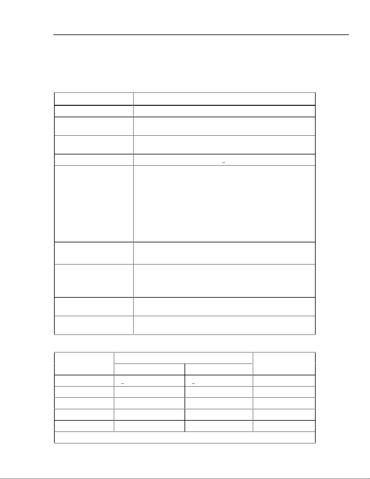
Introduction
The 268XA Service Manual supports the performance testing, calibration, servicing, and
maintenance of the 2680A Data Acquisition System (DAS), the 2686A Data Logging
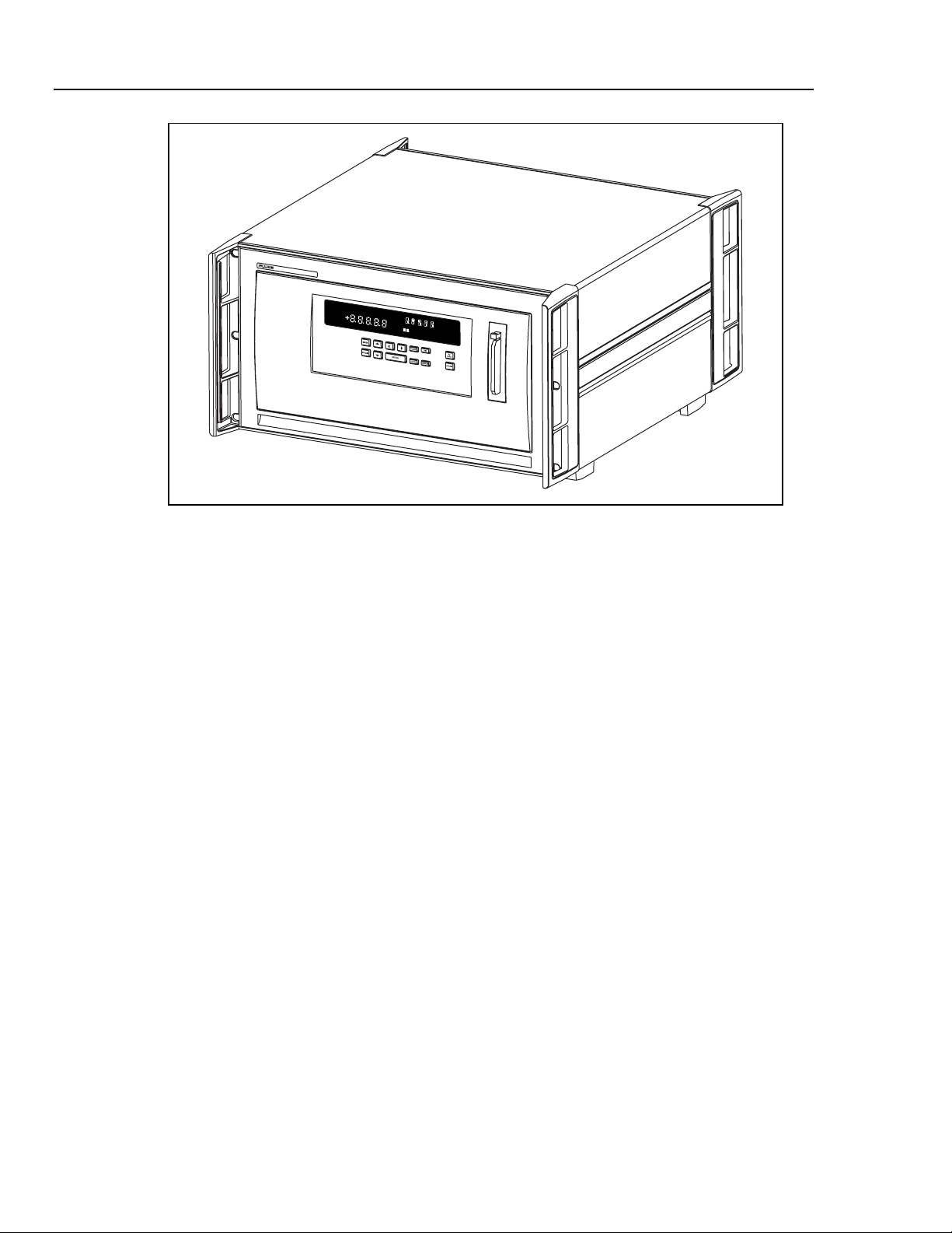
System (DLS) and modules. See Figure 1-1 for a view of the 268XA.
The 2686A comes with a removable PC Card (PCMCIA) for stand-alone storage
operation. This socket accepts ATA memory cards up to 2 GB in size.
Each 268XA device can hold from 1 to 6 analog modules. These modules are the
Precision Analog module (PAI), Fast Analog module (FAI), and the Digital IO/Relay and
Totalizer module (DIO). These modules are all isolated from one another. You can add
the DIO module to the device in slot 6 only.
The analog modules measure dc volts, ac volts, ohms, temperature, frequency, and dc
current. Temperature measurements use thermocouples, thermistors or resistance
temperature detectors (RTDs). The devices also have extensive computed math
capability. Besides using data collected from the analog modules and digital totalizer,
time can also be used in computed channel calculations.
The system scans 20 to 120 analog channels and calculates the values for up to 60
computed channels. Interval timers, alarm conditions, and/or an external signal input can
trigger scans. The Fluke DAQ software configures and controls up to 99 268XA devices
via an Ethernet connection. The software provides the means to view scan data and log it
into files.
Introduction and Specifications
Introduction
1
The analog modules that may be used with the 268XA are the FAI module and the PAI
module. The PAI modules emphasize precision with 5 ½ digits of resolution, .02%
accuracy, and can withstand up to 150 V common mode voltage (300 V on channels 1
and 11). The FAI modules emphasize increased measurement speed with 4 ½ digits of
resolution, 0.04% accuracy, and can withstand up to 50 V common mode voltage. Device
specifications are provided later in this chapter.
1-3
Page 20
268XA
Service Manual
2680 SERIES DAQ SYSTEM
REVIEW
MAX
REM
LAST
SCAN
MIN
AUTO
SET
FUNC
MON
Mx+B
F
ALARM
C F RO
mV AC DC
LIMIT
x1Mk
HI
Hz
OFF
PRN
12
CH
LO
CAL
EXT
TR
Figure 1-1. 2680A/2686A Device
alg46f.eps
1-4
Page 21
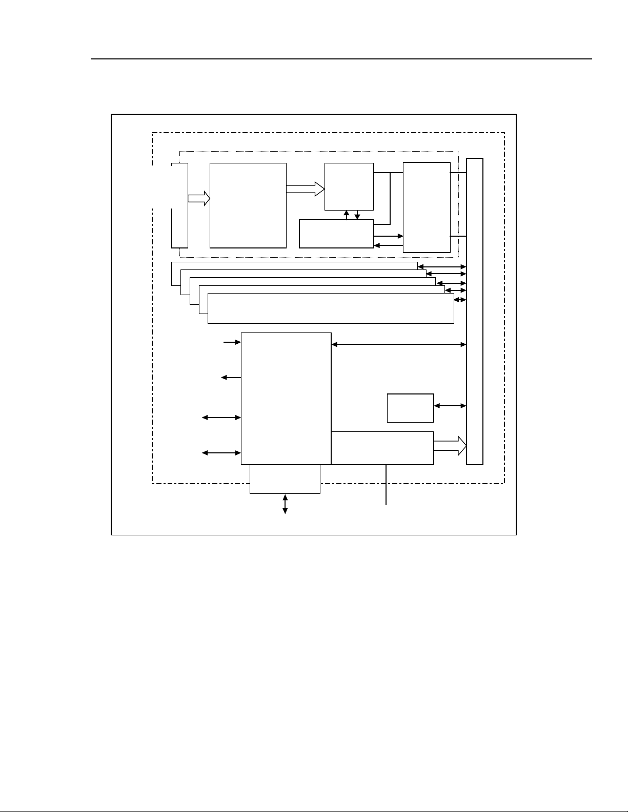
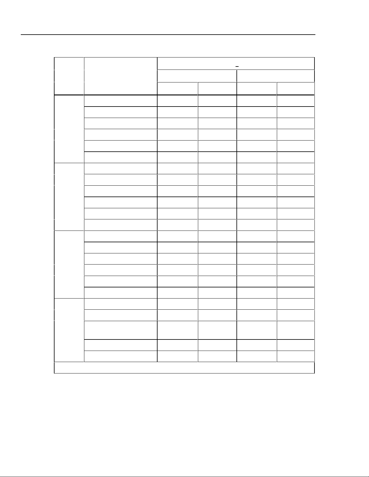
Block Diagrams
Removable 20
channel input
port with built in
temp sensor
A/D #2
A/D #3
A/D #4
External Trig in
External Trig out
TCP/IP
Network
A/D Input Card (one of six)
Switch Matrices
(FET or Relay)
A/D #5
DIO or A/D #6
Controller
RAM
FLASH
Real Time clock
Ethernet
Filter
and
A/D
circuits
Ctrl
Microprocessor
Data
Power
Data
Ctrl
Introduction and Specifications
Block Diagrams
Isolated
Power
Power
Daughter
Card
Optoisolators
Display/
Keypad
M
o
t
h
e
r
b
o
a
r
d
/
C
o
n
t
r
o
l
l
e
r
1
RS232
(cal/test)
RS232
PCMCIA Type II
Memory Slot
ATA Card
Figure 1-2. 268XA Chassis
A/C and Battery
Supply Circuits
Line Voltage or
Battery Voltage
DC
Power
Bus
alg50f.eps
1-5
Page 22
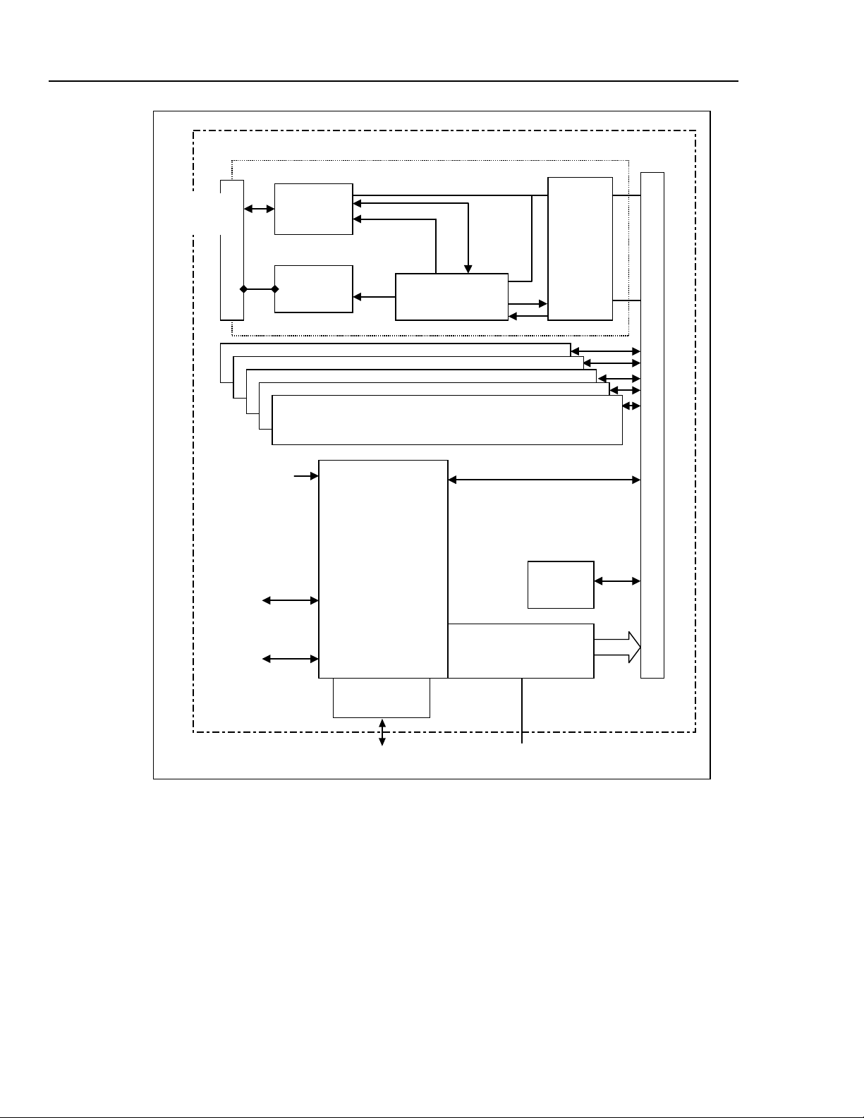
268XA
Service Manual
Digital I/O Output Card
Removable
Connector
Card
A/D #1
External Trig in
Tcp/IP
Network
A/D #2
A/D #3
Digital I/O
Totalizer (1)
A/D #4
A/D #5
(20) and
Relay
Contact
(8 pr)
Ctrl
Controller
RAM
FLASH
Real Time clock
Ethernet
Ctrl
Microprocessor
and drivers
Data
Data
Ctrl
Isolated
Power
Power
Daughter
Card
Optoisolators
Display/
Keypad
M
o
t
h
e
r
b
o
a
r
d
/
C
o
n
t
r
o
l
l
e
r
RS232
(cal/test)
A/C and Battery
RS232
PCMCIA Type II
Memory Slot
ATA Card
Supply Circuits
Line Voltage or
Battery Voltage
Figure 1-2. 268XA Chassis (cont)
DC
Power
Bus
alg51f.eps
1-6
Page 23

Specifications
Specifications are divided into four sections. The first section contains the specifications
that apply to both the 2680A and 2686A devices. The second section contains
specifications that apply only to the Precision A/D Input (PAI) module. The third section
contains specifications that apply only to the Fast A/D Input (FAI) module. The last
section contains informat ion on ly for the dig ita l I/O rela y an d the tota li zer (D IO ) mo dule .
2680A/2686A Combined Specifications
The following specifications apply to both the 2680A and 2686A devices. The topics
include:
• General Specifications
• PAI/FAI Environmental Specifications
• DIO Digital I/O and Totalizer Interface
Introduction and Specifications
Specifications
1
1-7
Page 24

268XA
Service Manual
2680A/2686A General Specifications
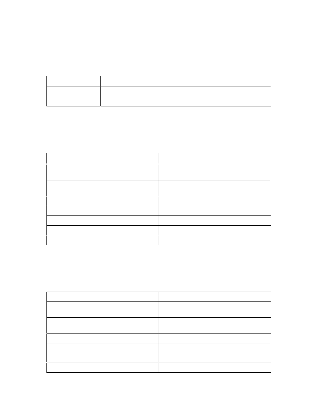
Table 1-1 provides the general specifications for the 2680A and 2686A devices.
Table 1-1. 268XA General Specifications
Specification Characteristic
Input Channel Capacity Maximum of 120 channels (Precision or Fast Analog Input) per
chassis
Optional DIO 20 digital input and outputs channels, 8 double pole-single throw
relay channels, a totalizer input, and a totalizer enable input.
Computed Channels 60
Size 473 mm (18.6 in) x 423 mm (17 in) x 237 mm (9.3 in)
Weight 2680A/2686A (empty) 8.5 kg (18.9 lb)
2680A – FAI 0.8 kg (1.8 lb)
2680A – PAI 1.2 kg (2.7 lb)
2680A – DIO 0.8 kg (1.8 lb)
Power 100 – 240 V ac (no switching required), 50 to 60 Hz, 100 VA
maximum or optional 9 V dc to 45 V dc, 35 W maximum
EMC EN50082-2
EN55022-1
EN55011 class A
EN610000-4-2,3,4,6,8
EN61326
Safety EN61010-1, CAT II (DIO is rated CAT I) CSA C22.2 No. 1010.1
Serial Interface Connector: 9 pin male (DB9)
Signals: Tx, Rx, DTR, RTS, GND
Modem Control: full duplex
Baud rates: 4800, 9600, 19200, 38400 (19,200 default)
Data format: 8 data bits, no parity, one stop bit
Flow Control: XON/XOFF
Echo: off
Common Mode Voltage Precision Analog Input: 150 (300 on channels 1 and 11) Fast
Analog Input: 50 V dc or 30 V ac rms
Operating Temperature Range -20 oC to 60 oC (-4 oF to +140 oF)
Storage Temperature Range -40 oC to 70 oC (-40 oF to +158 oF)
Relative Humidity 90% maximum for -10 oC to 28 oC (14 oF to +82 oF)
75% maximum for 28
50% maximum for 35
(3 MΩ range, reduce humidity rating by 25% for 1 hour warm-up.
3 MΩ range meets full humidity ratings with 2 hour warm-up)
o
C to 35 oC (82 oF to +95 oF)
o
C to 60 oC (95 oF to +140 oF)
1-8
Altitude Operating: 2,000 m (6,561 ft) maximum
Non-operating: 12,200 m (40,000 ft) maximum
Warm-up Time 1 hour to rated specifications -or- 15 minutes if relative humidity
(non-condensing) is 50% or less.
Page 25
Introduction and Specifications
Real-Time Clock and Calendar
Real-Time Clock and Calendar
The next table provides a summary of the battery powered real-time clock and calendar.
Table 1-2. 268X Real-Time Clock and Calendar
Specification Characteristic
Accuracy 1 minute per month for 0 °C to 50 °C range
Battery Life >5 unpowered device years for 20 °C to 28 °C (68 °F to 82.4 °F).
Trigger In Specifications
The following table provides a summary of the Trigger In specifications. The Trigger In
input is located on the rear panel connector, terminals Trigger In and Signal GND.
Table 1-3. Trigger In Specification
Specification Characteristic
Logical High - Trigger not set Minimum: 2.0 V
Maximum: 7.0 V
1
Logical Low - Trigger set Minimum: -0.6 V
Maximum: +0.8 V
Compatibility TTL or Contact Closure
Isolation None (dc coupled)
Minimum Pulse Width 5 µs
Maximum Frequency Nominal 400 Hz
Repeatability 3 ms
Trigger Out Specifications
The next table provides a summary of the Trigger Out specifications. The Trigger Out
output is located on the rear panel connector, terminals Trigger Out and Signal GND.
Table 1-4. Trigger Out Specification
Specification Characteristic
TTL Logical Zero - Trigger Out Set 0.8 V maximum for an Iout of -1.0 mA (1 LSTTL
load)
TTL Logical One - Trigger Out Not Set 3.8 V minimum for an Iout of 0.05 mA (1 LSTTL
load)
Non-TTL Logical Zero - Trigger Out Set 1.8 V maximum for an Iout of -20 mA
Non-TTL Logical One - Trigger Out Not Set 3.25 V minimum for an Iout of -50 mA
Pulse Duration (Logic Low) 125 µs
Isolation None
1-9
Page 26
268XA
Service Manual
Master Alarm Output Specification
Communication I/O
The following specifications cover the Master Alarm output. The Master Alarm output is
located on the rear panel connector, terminals Master Alarm, and Signal GND.
Table 1-5. Master Alarm Output Specification
Specification Characteristic
Output Voltage - TTL Logical Zero 0.8 V maximum for an Iout of -1.0 mA (1 LSTTL
load)
Output Voltage - TTL Logical One 3.8 V minimum for an Iout of 0.05 mA (1 LSTTL
load)
Output Voltage - Non-TTL Load Zero 1.8 V maximum for an Iout of -20 mA
Output Voltage - Non-TTL Load One 3.25 V minimum for an Iout of -50 mA
Communication with 268XA devices can be accomplished through either a 10/100BaseT
interface or through an RS-232 port. The 10/100BaseT provides the primary
communication interface. The RS-232 is used for calibration and limited debug
capability.
2686A PC Card Storage
The 2686A supports a non-volatile PC Card (PCMCIA ATA type card) memory module
option. This table provides a list of active channels and the number of scans to memory
card capacity. The standard Controller card will store approximately 600,000 readings.
Table 1-6. 2686A - Active Channels and Number of Scans to Card Capacity
Memory Card/
Active Channels 20 ch 40 ch 60 ch 80 ch 100 ch 120 ch
16 MB 100,548 66,765 50,074 40,059 33,382 28,613
128 MB 800,000 528,000 400,000 320,000 264,000 224,000
256 MB 1.6 M 1.056 M 800,000 640,000 528,000 448,000
512 MB 3.2 M 2.112 M 1.6 M 1.28 M 1.056 M 896,000
1 GB 6.2 M 4.224 M 3.2 M 2.56 M 2.112 M 1.792 M
Estimating space: 80 bytes/scan + 4 bytes/channel scanned (allow 4.5% overhead for card formatting)
1-10
Page 27

Introduction and Specifications
Precision Analog Input (PAI) A/D Specifications
Precision Analog Input (PAI) A/D Specifications
This section includes specifications specific to the PAI A/D instrument by measurement
function.
Specifications PAI A/D DC Voltage Measurement
The following tables provide PAI A/D specifications for the dc voltage measurement
function.
Table 1-7. PAI A/D DC Voltage General Specifications
Specification Characteristic
Input Impedance 100 MΩ in parallel with 300 pF maximum for ranges <=3 V
10 MΩ in parallel with 100 pF maximum for ranges >3 V
Normal Mode Rejection 50 dB minimum at 50 Hz/60 Hz +0.1%, Slow Rate
Common Mode Rejection 120 dB minimum at dc, 50 Hz/60 Hz +0.1%, 1 kΩ imbalance, Slow
Rate
80 dB minimum at dc, 50 Hz/60 Hz +0.1%, 1 kΩ imbalance, Medium
and Fast Rates
1
Channel-to-Channel Cross talk 120 dB minimum Slow Rate (e.g., 30 V dc on channel 1 may cause a
30 µV error on channel 2)
100 dB minimum Medium and Fast Rates (e.g., 1V dc on channel 1
may cause a 10 µV error on channel 2)
Temperature Coefficient For % input: Add 1/10th the 90-day specification per °C above 28 °C or
below 18 °C
For floor error (V): Add 1/20th the 90-day specification per °C above
28 °C or below 18 °C
Accuracy at -20 °C Multiply the -10 °C to +60 °C accuracy specification by 2. After 1 hour
warm-up. For accurate between -10 °C and -20 °C, interpolate linearly.
Maximum Input Voltage The lesser voltage of:
300 V from any terminal on channels 1 and 11 to earth;
150 V from any terminal on channels 2 through 10, and 12 through 20
to earth;
300 V from any terminal on channels 1 and 11 to any other terminal;
150 V from any terminal on channels 2 through 10, and 12 through 20
to any other input terminal
1-11
Page 28
268XA
Service Manual
Table 1-8. PAI A/D DC Voltage Range and Resolution Specifications
Resolution
Range
Slow Fast
90 mV 0.3 µV1 µV
300 mV 1 µV3 µV
3 V 10 µV 30 µV
30 V 100 µV 300 µV
150/300 V 1 mV 3 mV
Note 300 V range applies to channels 1 and 11 only.
Table 1-9. PAI A/D DC Voltage Accuracy Specifications
Accuracy, 3σ + (% input + V)
18 °C to 28 °C -10 °C to 60 °C
Range
90 Day 1 Year 1 Year
Slow Fast Slow Fast Slow Fast
90 mV .01%+7 µV .01%+17 µV .013%+8 µV .013%+18 µV .042%+18.2 µV .042%+44.2 µV
300 mV .01%+15 µV .01%+30 µV .013%+17 µV .013%+35 µV .042%+39 µV .042%+78 µV
750 mV* .01%+40 µV .01%+70 µV .013%+50 µV .013%+80 µV .042%+104 µV .042%+182 µV
3 V .01%+0.1 mV .01%+0.2 mV .013%+0.15 mV .013%+0.2 mV .042%+0.26 mV .042%+0.52 mV
30 V .01%+1.5 mV .02%+3 mV .013%+1.7 mV .026%+3.5 mV .042%+3.9 mV .084%+7.8 mV
150/300 V* .01%+15 mV .04%+30 mV .013%+17 mV .052%+35 mV .042%+39 mV .168%+78 mV
* 300 V range applies to channels 1 and 11 only.
1-12
Page 29
Introduction and Specifications
Precision Analog Input (PAI) A/D Specifications
PAI A/D AC Voltage Measurement Specifications
The following tables provide PAI A/D specifications for the ac voltage measurement
function.
Table 1-10. PAI A/D AC Voltage General Specifications
Specification Characteristic
Input Impedance 1 MΩ in parallel with 100 pF
Maximum Crest Factor 3.0 Maximum
2.0 for rated accuracy
Crest Factor Error For nonsinusoidal input signals with crest factors between 2 and 3 and
pulse widths >=100 µs, add 0.2% to the accuracy specifications.
Common Mode Rejection 80 dB minimum at dc, 50 Hz/60 Hz +0.1%, 1 kΩ imbalance, Slow Rate
Maximum Input Voltage The lesser voltage of:
300 V ac rms from any terminal on channels 1 and 11 to earth.
150 V ac rms from any terminal on channels 2 through 10, and 12
through 20 to earth.
1
300 V ac rms from any terminal on channels 1 and 11 to any other
terminal.
150 V ac rms from any terminal on channels 2 through 10 and 12
through 20 to any other input terminal.
Maximum Volt-Hertz Product 2x10⁶ Volt-Hertz product on any range, normal mode input.
1x10⁶ Volt-Hertz product on any range, common mode input.
Temperature Coefficient Linear interpolation between 2 applicable points for temperatures
between 28 °C and 60 °C, or -10 °C and 18 °C, e.g., if the applicable
specification at 28 °C is 2% and the specification at 60 °C is 3%, then
the specification at 40 °C is (3%-2%)x(40-28)/(60-28)+2%=2.375%.
Accuracy at -20 °C Multiply the -10 °C to +60 °C accuracy specification by 2. After 1 hour
warm-up. For accuracy between -10 °C and -20 °C, interpolate lin early .
DC Component Error The presence of a dc voltage will cause an indeterminate error in the
reading of the ac voltage on the input.
Table 1-11. PAI A/D AC Voltage Range and Resolution Specifications
Range Resolution Minimum Input for
Slow Fast Rate Accuracy
Full Scale +30,000 +3,000
300 mV 10 µV 100 µV 20 mV
3 V 100 µV 1 mV 200 mV
30 V 1 mV 10 mV 2 V
150/300 V 10 mV 100 mV 20 V
Note 300 V range applies to channels 1 and 11 only.
1-13
Page 30
268XA
Service Manual
Table 1-12. PAI A/D AC Voltage Accuracy Specifications
1 Year Accuracy + (%input + V) [1]
Range Frequency 18 °C to 28 °C -10 °C to 60 °C
Slow Fast Slow Fast
300 mV 20 to 50 Hz 3%+.25 mV 6%+.5 mV 3.5%+.25 mV 7%+.5 mV
50 to 150 Hz 0.4%+.25 mV 1%+.5 mV 0.5%+.25 mV 1.5%+.5 mV
150 Hz to 10 kHz 0.3%+.25 mV 1%+.5 mV 0.4%+.25 mV 1.5%+.5 mV
10 kHz to 20 kHz 0.4%+.25 mV 1%+.5 mV 0.7%+.25 mV 1.5%+.5 mV
20 kHz to 50 kHz 2%+.3 mV 3%+.5 mV 3%+.3 mV 4%+.5 mV
50 kHz to 100 kHz 5%+.5 mV 5%+1 mV 7%+.5 mV 8%+1 mV
3 V 20 to 50 Hz 3%+2.5 mV 6%+5 mV 3.5%+2.5 mV 7%+5 mV
50 to 150 Hz 0.4%+2.5 mV 1%+5 mV 0.5%+2.5 mV 1.2%+5 mV
150 Hz to 10 kHz 0.3%+2.5 mV 1%+5 mV 0.4%+2.5 mV 1.2%+5 mV
10 kHz to 20 kHz 0.4%+2.5 mV 1%+5 mV 0.5%+2.5 mV 1.2%+5 mV
20 kHz to 50 kHz 1%+3 mV 1.5%+6 mV 1.5%+3 mV 2%+6 mV
50 kHz to 100 kHz 2%+5 mV 3%+10 mV 3%+5 mV 4%+10 mV
30 V 20 to 50 Hz 3%+25 mV 6%+50 mV 3.5%+25 mV 7%+50 mV
50 to 150 Hz 0.4%+25 mV 1%+50 mV 0.5%+25 mV 1.2%+40 mV
150 Hz to 10 kHz 0.3%+25 mV 1%+50 mV 0.5%+25 mV 1.2%+40 mV
10 kHz to 20 kHz 0.4%+25 mV 1%+50 mV 0.5%+25 mV 1.2%+40 mV
20 kHz to 50 kHz 1%+30 mV 1.5%+60 mV 1%+30 mV 2%+50 mV
50 kHz to 100 kHz, V<20V 2%+50 mV 3%+100 mV 2.5%+50 mV 4%+100 mV
150/300 V 20 to 50 Hz 3%+.25 V 6%+.5 V 3.5%+.25 V 7%+.5 V
50 to 150 Hz 0.4%+.25 V 1%+.5 V 0.5%+.25 V 1.2%+.4 V
150 Hz to 2 kHz
Vx Hz<2 x10
6
0.3%+.25 V 1 .2%+.5 V 0.5%+.25 V 1.4%+.4 V
2 kHz to 20 kHz, V<100V 0.4%+.25 V 1.6%+.5 V 0.5%+.25 V 1.8%+.4 V
20 kHz to 50 kHz, V<40V 1%+.30 V 2 .0%+.6 V 1.2%+.30 V 2.5%+.5 V
[1] Sinewave inputs>6% of scale and signals with crest factors <2.
1-14
Page 31

Introduction and Specifications
Precision Analog Input (PAI) A/D Specifications
PAI A/D 4-Wire Resistance Measurement Specifications
The following tables provide PAI A/D specifications for the 4-wire resistance
measurement function. The 4-wire measurements use 2 input channels a decade apart,
e.g., channels 4 and 14.
Table 1-13. PAI A/D 4-Wire Resistance Temperature Coefficient
Specification Characteristic
Temperature Coefficient Add 1/10th the 90 day specification per °C above
28 °C or below 18 °C.
Accuracy at -20 °C Multiply the -10 °C to +60 °C accuracy
specification by 2. After 1 hour warm-up. For
accuracy between -10 °C and -20 °C, interpolate
linearly.
Table 1-14. PAI A/D 4-Wire Resistance Range and Resolution Specifications
1
Resolution
Range Slow Fast
300 Ω 1 mΩ 3mΩ 1 mA 300 mV 3.5 V
3 kΩ 10 mΩ 30 mΩ 100 µA 300 mV 3.5 V
30 kΩ 100 mΩ 300 mΩ 10 µA 300 mV 3.5 V
300 kΩ 1 Ω 3 Ω 10 µA 3.0 V 3.5 V
3 MΩ 10 Ω 30 Ω 1 µA 3.0 V 3.5 V
Table 1-15. PAI A/D 4-Wire Resistance Accuracy Specifications
Range
300 Ω .015%+20 mΩ .02%+80 mΩ .02%+50 mΩ .02%+120 mΩ .084%+126 mΩ .084%+336 mΩ
3 kΩ .02%+.3 Ω .02%+.8 Ω .02%+.5 Ω .02%+1.2 Ω .084%+1.26 Ω .084%+3.36 Ω
30 kΩ .03%+3 Ω .04%+10 Ω .03%+5 Ω .04%+15 Ω .126%+12.6 Ω .168%+42 Ω
90 Day 1 Year 1 Year
Slow Fast Slow Fast Slow Fast
Current Full Scale Maximum Voltage
Applied Voltage Applied by Instrument
Accuracy, 3σ + (% input + V)
18 °C to 28 °C -10 °C to 60 °C
300 kΩ .1%+40 Ω .2%+100 Ω .1%+60 Ω .2%+150 Ω .42%+168 Ω .84%+420 Ω
3 MΩ [1] .25%+800 Ω .5%+10 kΩ .25%+1 kΩ .5%+1.5 kΩ 1. 05%+3.36 kΩ 2.1%+4.2 kΩ
[1] The 3 MΩ range is susceptible to the absorption of humidity under extreme conditi ons. If the i nst rument is
operated normally within its specified temperat ure-hum i dity range, the 3 MΩ range meets its accuracy specifications.
However, if the instrument is “soaked” at 50 °C, 90% relative humidity, the 3 MΩ range may require 1 hour of “dryout” time at 25 °C, <40% relative humidity for each hour of soak time in order to achieve its specified accuracy.
1-15
Page 32

268XA
Service Manual
PAI A/D 2-Wire Resistance Measurement Specifications
PAI A/D 4-Wire RTD per ITS-1990 Measurement Specifications
The PAI A/D specifications for the two-wire resistance measurement function is based on
the four-wire resistance measurement specification (above) except you add a nominal 5 Ω
(10 Ω maximum) positive offset. This value varies for each channel and with temperature
(nominal +1%/ºC).
The following tables provide PAI A/D specifications for the 4-wire ResistanceTemperature Detector (RTD) measurement function. The 4-wire measurements use 2
input channels a decade apart, e.g., channels 4 and 14.
Table 1-16. PAI A/D 4-Wire RTD Temperature Coefficient
Specification Characteristic
Temperature Coefficient To calculate RTD accuracy for temperatures between 28 °C and 60 °C,
or -10 °C and 18 °C, use a linear interpolation between the two
applicable points. For example, if the applicable specification at 28 °C
is 0.2 and the specification at 60 °C is 0.75, then the specification at
40 °C is =(.75-.2)x(40-28)/(60-28)+.2=0.406.
Accuracy at -20 °C Multiply the -10 °C to +60 °C accuracy specification by 2. After 1 hour
warm-up. For accuracy between -10 °C and -20 °C, interpolate lin early .
Table 1-17. PAI A/D 4-Wire RTD Specifications
Accuracy, 3σ
Resolution
Temperature
Slow Fast Slow Fast Slow Slow Fast
-200 °C 0.003 °C 0.007 °C0.06 °C0.16 °C 0.09 °C0.33 °C0.63 °C
0 °C 0.003 °C 0.007 °C0.09 °C0.20 °C 0.13 °C0.53 °C0.86 °C
100 °C 0.003 °C 0.007 °C0.10 °C0.23 °C 0.16 °C0.63 °C0.97 °C
300 °C 0.003 °C 0.007 °C0.14 °C0.30 °C 0.21 °C0.83 °C1.20 °C
600 °C 0.003 °C 0.007 °C0.19 °C0.53 °C 0.30 °C1.20 °C1.60 °C
90 Day
18 °C to 28 °C
1 Year
18 °C to 28 °C
1 Year
–10 °C to 60 °C
PAI A/D 2-Wire RTD per ITS-1990 Measurement Specifications
The PAI A/D specifications for the two-wire Resistance Temperature Detector (RTD)
measurement function is based on the four-wire RTD measurement specification (above)
except you add a nominal 5 Ω (approximately 13 °C) positive offset. This value varies for
each channel and temperature gradient (nominal +1%/ºC). Also note that the resistance of
the RTD wiring adds directly to the error. After 100 million operations of a measurement
channel, the offset will increase at an indeterminate rate.
1-16
Page 33

Introduction and Specifications
Precision Analog Input (PAI) A/D Specifications
PAI A/D Thermocouple per ITS-1990 Measurement Specifications
The following tables provide PAI A/D specifications for the thermocouple measurement
function per ITS-1990.
Table 1-18. PAI A/D Thermocouple General Specifications
Specification Characteristic
Input Impedance 100 MΩ minimum in parallel with 300 pF
Open Thermocouple Detect Operates by injecting a small ac signal into the
input after each measurement. A thermocouple
resistance greater than 1k to 10k is detected as
an open input.
Temperature Coefficient To calculate Thermocouple accuracy for
temperatures between 28 °C and 60 °C,
or -10 °C and 18 °C, use a linear interpolation
between the two applicable points. For example,
if the applicable specification at 28 °C is 0.6 and
the specification at 60v°C is 1.1, then the
specification at 40v°C is =(1.1-0.6)x(40-28)/(60-
28)+0.6=0.7875.
1
Accuracy at -20 °C Multiply the -10 °C to +60 °C accuracy
specification by 2. After 1 hour warm-up. For
accuracy between -10 °C and -20 °C, interpolate
linearly.
1-17
Page 34

268XA
Service Manual
Table 1-19. PAI A/D Thermocouple Specifications
Accuracy + °C
Thermocouple Resolution 18 °C to 28 °C -10 °C to 60 °C
ITS90 °C 90 Day 1 Year 1 Year
Type Temperature °C Slow Slow Fast Slow Fast
B 600 to 900 0.2 1.20 1.40 3.10 1.50 3.20
900 to 1200 0.2 0.90 1.00 2.20 1.20 2.40
1200 to 1820 0.1 0.75 1.00 1.90 1.30 2.20
C 0 to 150 0.2 0.80 0.90 1.60 1.00 1.70
150 to 650 0.1 0.65 0.75 1.40 1.00 1.50
650 to 1000 .05 0.65 0.85 1.40 1.20 1.80
1000 to 1800 .05 1.00 1.30 2.10 2.10 2.80
1800 to 2316 .05 1.60 2.10 3.20 3.40 4.60
E -100 to –25 .03 0.45 0.50 0.80 0.60 0.80
-25 to 20 .02 0.35 0.40 0.60 0.50 0.70
20 to 600 .02 0.30 0.40 0.60 0.50 0.80
600 to 1000 .02 0.40 0.50 0.70 0.90 1.00
J -100 to 80 .03 0.45 0.50 0.80 0.60 0.80
80 to 230 .02 0.35 0.50 0.70 0.60 0.80
230 to 760 .02 0.40 0.50 0.70 0.80 0.90
K -100 to –25 .04 0.55 0.60 0.90 0.70 1.00
-25 to 120 .03 0.40 0.50 0.80 0.60 0.90
120 to 800 .03 0.50 0.65 0.90 1.00 1.20
800 to 1372 .03 0.70 1.00 1.30 1.60 1.90
L -100 to 100 .04 0.90 1.00 2.00 1.30 2.00
100 to 800 .04 0.50 0.90 1.40 1.20 1.70
800 to 900 .03 0.50 0.70 1.10 1.30 1.50
1-18
Page 35

Introduction and Specifications
Precision Analog Input (PAI) A/D Specifications
Table 1-19. PAI A/D Thermocouple Specifications (cont.)
Accuracy + °C
Thermocouple Resolution 18 °C to 28 °C -10 °C to 60 °C
ITS90 °C 90 Day 1 Year 1 Year
Type Temperature °C Slow Slow Fast Slow Fast
N -100 to –25 .05 0.65 0.75 1.20 0.80 1.30
-25 to 120 .05 0.55 0.60 1.00 0.70 1.10
120 to 1000 .04 0.45 0.60 0.90 1.00 1.20
1000 to 1300 .03 0.55 0.75 1.00 1.20 1.50
R 250 to 600 0.1 0.90 1.00 2.10 1.20 2.20
600 to 1500 0.1 0.80 0.90 1.80 1.30 2.00
1500 to 1767 0.1 0.85 0.85 1.90 1.70 2.50
S 250 to 1000 0.1 0.95 1.10 2.30 1.30 2.40
1
1000 to 1400 0.1 0.80 1.00 1.90 1.40 2.30
1400 to 1767 0.1 1.00 1.30 2.20 1.80 2.80
T -100 to 0 .04 0.60 0.65 1.00 0.70 1.10
0 to 150 .03 0.40 0.50 0.80 0.60 0.90
150 to 400 .02 0.30 0.40 0.60 0.60 0.80
U -100 to 0 .04 1.50 1.50 2.60 1.60 3.00
0 to 600 .04 0.60 0.80 1.60 1.10 1.90
Thermistor
Accuracy + °C
90 Day 1 Year
Temp °C Range*
-40 to 150 100 to 100 mΩ 0.3 0.4 18 to 23 °C
Steinhart – Hart Equation: 1/(T oKelvin) = A + B*(ln Ω) + C*(ln Ω)
Default constants are supplied only for a YSI (type 004) 2,252 Ω thermistor, you can enter
constants for other thermistors. The ranges of thermistor constants are as follows: A 1.0E-4 to
1.0E-2, B 1.0E-5 to 1.0E-3, and C 1.0E-8 to 1.0E-6.
*Assumes 4-wire measurement for thermistor resistance values below 2 kΩ (above 28 °C for a
2.252 kΩ thermistor).
Slow Slow
3
1-19
Page 36

268XA
Service Manual
PAI A/D Frequency Measurement Specifications
The following tables provide PAI A/D specifications for the frequency measurement
function.
Table 1-20. PAI A/D Frequency Accuracy Specifications
Frequency Measurement Accuracy, 1 Year, -10 °C to 60 °C
Range Resolution Accuracy + (% input + Hz)
Slow Fast Slow Fast
15 Hz to 900 Hz 0.01 Hz 0.1 Hz 0.05%+0.02 Hz 0.05%+0.2 Hz
900 Hz to 9 kHz 0.1 Hz 1 Hz 0.05%+0.1 Hz 0.05%+1 Hz
9 kHz to 90 kHz 1 Hz 10 Hz 0.05%+1 Hz 0.05%+10 Hz
90 kHz to 900 kHz 10 Hz 100 Hz 0.05%+10 Hz 0.05%+100 Hz
1 MHz 100 Hz 1 kHz 0.05%+100 Hz 0.05%+1 kHz
Table 1-21. PAI A/D Frequency Sensitivity Specifications
Frequency Measurement Sensitivity (Sinewave)
Frequency Range Minimum Signal Maximum Signal
15 Hz to 70 kHz 100 mV ac rms V<150/300 V rms [1] and Vx Hz<2x10⁶)
70 kHz to 100 kHz 100 mV ac rms 20 V ac rms
100 kHz to 200 kHz 150 mV ac rms 10 V ac rms
200 kHz to 300 kHz 150 mV ac rms 7 V ac rms
300 kHz to 1 MHz Linearly increasing from 150
mV ac rms at 300 kHz to 2 V ac
rms at 1 MHz
[1] 300 V range applies to channels 1 and 11 only.
Linearly decreasing from 7 V ac rms at
300 kHz to 2 V ac rms at 1 MHz
1-20
Page 37

Introduction and Specifications
Fast Analog Input (FAI) A/D Specifications
Fast Analog Input (FAI) A/D Specif ic ations
This section includes specifications specific to the FAI A/D instrument by measurement
function.
FAI A/D DC Voltage Measurement Specifications
The following tables provide FAI A/D specifications for the dc voltage measurement
function.
Table 1-22. FAI A/D DC Voltage General Specifications
Specification Characteristic
Input Impedance 100 MΩ in parallel with 300 pF maximum for ranges <=3 V
10 MΩ in parallel with 100 pF maximum for ranges >3 V
Normal Mode Rejection 50 dB minimum at 50 Hz/60 Hz +0.1%, Slow Rate
1
Common Mode
Rejection
Channel-to-Channel
Crosstalk
Temperature Coefficient For % input: Add 1/10th the 90-day specification per °C above 28°C or
Accuracy at -20 °C Multiply the -10 °C to +60 °C accuracy specification by 2. After 1 hour
Maximum Input Voltage The lesser voltage of:
Table 1-23. FAI A/D DC Voltage Resolution and Repeatability Specifications
120 dB minimum at dc, 50 Hz/60 Hz +0.1%, 1 kΩ imbalance, Slow Rate
80 dB minimum at dc, 60 dB at 50 Hz/60 Hz +0.1%, 1 kΩ imbalanc e,
Medium and Fast Rates
120 dB minimum Slow Rate (e.g., 30 V dc on channel 1 may cause a
30 µV error on channel 2)
80 dB minimum Medium and Fast Rates (e.g., 1 V dc on channel 1 may
cause a 10 µV error on channel 2)
below 18°C.
For floor error (V): Add 1/20th the 90-day specification per °C above 28 °C
or below 18 °C.
warm-up. For accurate between -10 °C and -20 °C, interpolate linearly.
50 V dc or 30 V ac rms from any input terminal to earth
-or50 V dc or 30 V ac rms from any input terminal to any other input terminal
Resolution
Range
90 mV 3 µV6 µV
300 mV 1 µV3 µV
3 V 10 µV30 µV
30 V 100 µV 300 µV
50 V 1 mV 3 mV
Slow Fast
1-21
Page 38

268XA
Service Manual
FAI A/D AC Voltage Measurement Specifications
Table 1-24. FAI A/D DC Voltage Accuracy Specifications
Accuracy, 3σ + (% input + V)
18 °C to 28 °C -10 °C to 60 °C
Range
90 Day 1 Year 1 Year
Slow Fast Slow Fast Slow Fast
90 mV .01%+20 µV .01%+50 µV .013%+23 µV .013%+50 µV .042%+52 µV .042%+130 µV
300 mV .01%+40 µV .01%+90 µV .013%+49 µV .013%+93 µV .042%+104 µV .042%+234 µV
3 V .01%+.3 mV .01%+.6 mV .013%+.38 mV .013%+.64 mV .042%+.78 mV .042%+1.56 mV
30 V .01%+4 mV .02%+8 mV .013%+4.9 mV .026%+9.5 mV .042%+10.6 mV .084%+20.3 mV
50 V .01%+30 mV .04%+60 mV .013%+40 mV .052%+64 mV .042%+78 mV .168%+156 mV
The following tables provide FAI A/D specifications for the ac voltage function.
Table 1-25. FAI A/D AC Voltage General Specifications
Specification Characteristic
Input Impedance 1 MΩ in parallel with 100 pF
Maximum Crest Factor 3.0 maximum; 2.0 for rated accuracy
Crest Factor Error For nonsinusoidal input signals with crest factors between 2 and 3 and
pulse widths >=100 µs, add 0.2% to the accuracy specifications.
Common Mode Rejection 80 dB minimum at dc, 50 Hz/60 Hz +0.1%, 1 kΩ imbalance, Slow Rate
Maximum Input Voltage The lesser voltage of:
30 V ac rms from any input terminal to earth.
30 V ac rms from any terminal input to any other input terminal.
Maximum Volt-H ertz
Product
2x10⁶ Volt-Hertz product on any range, normal mode input.
6
Volt-Hertz product on any range, common mode input.
1x10
Temperature Coefficient Linear interpolation between 2 applicable points for temperatures
between 28 °C and 60 °C, or -10 °C and 18 °C, e.g., if the applicable
specification at 28 °C is 2% and the specification at 60 °C is 3%, then
the specification at 40 °C is (3%-2%)x(40-28)/(60-28)+2%=2.375%.
Accuracy at -20 °C Multiply the -10 °C to +60 °C accuracy specification by 2. After 1 hour
warm-up. For accuracy between -10 °C and -20 °C, interpolate lin early .
DC Component Error The presence of a dc voltage will cause an indeterminate error in the
reading of the ac voltage on the input.
1-22
Page 39

Introduction and Specifications
Fast Analog Input (FAI) A/D Specifications
Table 1-26. FAI A/D AC Voltage Range and Resolution Specifications
1
Range
Slow Fast
Full Scale +30,000 +3,000
300 mV 10 µV 100 µV 20 mV
3 V 100 µV 1 mV 200 mV
30 V 1 mV 10 mV 2 V
Table 1-27. FAI A/D AC Voltage Accuracy Specifications
Range Frequency 18°C to 28°C-10°C to 60°C
300 mV 20 to 50 Hz 3%+.25 mV 6%+.5 mV 3.5%+.25 mV 7%+.5 mV
50 to 150 Hz 0.4%+.25 mV 0.8%+.5 mV 0.5%+.25 mV 1%+.5 mV
150 Hz to 10 kHz 0.3%+.25 mV 0.8%+.5 mV 0.4%+.25 mV 1%+.5 mV
10 kHz to 20 kHz 0.4%+.25 mV 1%+.5 mV 0.7%+.25 mV 1.5%+.5 mV
20 kHz to 50 kHz 2%+.3 mV 3%+.5 mV 3%+.3 mV 4%+.5 mV
Resolution
1 Year Accuracy + (%input + V) [1]
Slow Fast Slow Fast
Minimum Input for
Rate Accuracy
50 kHz to 100 kHz 5%+.5 mV 5%+1 mV 7%+.5 mV 8%+1 mV
3 V 20 to 50 Hz 3%+2.5 mV 6%+5 mV 3.5%+2.5 mV 7%+5 mV
50 to 150 Hz 0.4%+2.5 mV 0.8%+5 mV 0.5%+2.5 mV 1%+5 mV
150 Hz to 10 kHz 0.3%+2.5 mV 0.6%+5 mV 0.4%+2.5 mV 1%+5 mV
10 kHz to 20 kHz 0.4%+2.5 mV 0.8%+5 mV 0.5%+2.5 mV 1%+5 mV
20 kHz to 50 kHz 1%+3 mV 1.5%+6 mV 1.5%+3 mV 2%+6 mV
50 kHz to 100 kHz 2%+5 mV 3%+10 mV 3%+5 mV 4%+10 mV
30 V 20 to 50 Hz 3%+25 mV 6%+50 mV 3.5%+25 mV 7%+50 mV
50 to 150 Hz 0.4%+25 mV 0.8%+50 mV 1.2%+25 mV 1.3%+40 mV
150 Hz to 10 kHz 0.4%+25 mV 0.8%+50 mV 1.2%+25 mV 1.3%+40 mV
10 kHz to 20 kHz 0.4%+25 mV 0.8%+50 mV 1.2%+25 mV 1.3%+40 mV
20 kHz to 50 kHz 1%+30 mV 1.5%+60 mV 1.2%+30 mV 2%+50 mV
50 kHz to 100 kHz, V<20V 2%+50 mV 3%+100 mV 2.5%+50 mV 4%+100 mV
[1] Sinewave inputs>6% of scale and signals with crest factors <2.
1-23
Page 40

268XA
Service Manual
FAI A/D 4-Wire Resistance Measurement Specifications
The following tables provide FAI A/D specifications for the 4-wire resistance
measurement function. The 4-wire measurements use 2 input channels a decade apart,
e.g., channels 4 and 14.
Table 1-28. FAI A/D 4-Wire Resistance Temperature Coefficient
Specification Characteristic
Temperature
Coefficient
Accuracy at -20 °C Multiply the -10 °C to +60 °C accuracy specification by 2. After 1 hour warm-
Table 1-29. FAI A/D 4-Wire Resistance Range and Resolution Specifications
Resolution
Range
300 Ω 10 mΩ 30 mΩ 1 mA 300 mV 3.5 V
3 kΩ 100 mΩ 300 mΩ 100 µA 300 mV 3.5 V
30 kΩ 1 Ω 3 Ω 10 µA 300 mV 3.5 V
300 kΩ 10 Ω 30 Ω 10 µA 3 .0 V 3.5 V
3 MΩ 100 Ω 300 Ω •1 µA 3.0 V 3.5 V
Range
Slow Fast
Table 1-30. FAI A/D 4-Wire Resistance Accuracy Specifications
90 Day 1 Year 1 Year
Add 1/10th the 90 day specification per °C above 28 °C or below 18 °C.
up. For accuracy between -10 °C and -20 °C, interpolate linearly.
Current Full Scale Maximum Voltage
Applied Voltage Applied by
Instrument
Accuracy, 3σ + (% input + Ω)
18 °C to 28 °C -10 °C to 60 °C
1-24
Slow Fast Slow Fast Slow Fast
300 Ω .02%+60 mΩ .02%+.1 Ω .02%+.1 Ω .02%+.2 Ω .084%+.25 Ω .084%+.42 Ω
3 kΩ .02%+.6 Ω .02%+2 Ω .02%+1 Ω .02%+3 Ω .084%+2.5 Ω .084%+8.4 Ω
30 kΩ .02%+6 Ω .2%+200 Ω .02%+10 Ω .2%+300 Ω .084%+25 Ω .84%+840 Ω
300 kΩ .5%+80 Ω 1%+2 kΩ .5%+150 Ω 1%+3 kΩ 2.1%+336 Ω 4.2%+8.4 kΩ
3 MΩ 1.3%+1 kΩ 2%+120 kΩ 1.3%+2 kΩ 2%+200 kΩ 5.46%+4. 2 kΩ 8.4%+200 kΩ
Page 41

Introduction and Specifications
Fast Analog Input (FAI) A/D Specifications
FAI A/D 2-Wire Resistance Measurement Specifications
The FAI A/D specifications for the two-wire resistance measurement function is based on
the four-wire resistance measurement specification (above) except you add a 700 to 1000
Ω positive offset. This value varies for each channel and temperature gradient (nominal
+1%/ºC).
FAI A/D 4-Wire RTD per ITS-1990 Measurement Specifications
The next tables provide FAI A/D specifications for the 4-wire Resistance-Temperature
Detector (RTD) measurement function. The 4-wire measurements use 2 input channels a
decade apart, e.g., channels 4 and 14. There is no 2-wire RTD capability for the FAI A/D.
Table 1-31. FAI A/D 4-Wire RTD Temperature Coefficient
Specification Characteristic
1
Temperature
Coefficient
Accuracy at -20 °C Multiply the -10 °C to +60 °C accuracy specification by 2. After 1 hour
Temperature Resolution
Slow Fast Slow Fast Slow Slow Fast
-200 °C 0.03 °C 0.06 °C 0.16 °C 0.25 °C 0.25 °C0.62 °C1.10 °C
0 °C 0.03 °C 0.06 °C 0.20 °C 0.31 °C 0.31 °C0.85 °C1.30 °C
100 °C 0.03 °C 0.06 °C 0.23 °C 0.34 °C 0.34 °C0.95 °C1.40 °C
300 °C 0.03 °C 0.06 °C 0.30 °C 0.41 °C 0.41 °C1.18 °C1.70 °C
600 °C 0.03 °C 0.06 °C 0.53 °C 0.63 °C 0.63 °C1.62 °C2.12 °C
To calculate RTD accuracy for temperatures between 28 °C and
60 °C, or -10 °C and 18 °C, use a linear interpolation between the two
applicable points. For example, if the applicable specification at 28 °C is 0.2
and the specifications at 60 °C is 0.75, then the specification at
40 °C =(.75-.2)x(40-28)/(60-28)+.2=.406.
warm-up. For accuracy between -10 °C and -20 °C, interpolate lin early .
Table 1-32. FAI A/D 4-Wire RTD Specifications
Accuracy, 3σ
90 Day
18 °C to 28 °C
1 Year
18 °C to 28 °C
1 Year
-10 °C to 60 °C
1-25
Page 42

268XA
Service Manual
FAI A/D Thermocouple per ITS-1990 Measurement Specifications
The following tables provide FAI A/D specifications for the thermocouple measurement
function per ITS-1990.
Table 1-33. FAI A/D Thermocouple General Specifications
Specification Characteristic
Input Impedance 100 MΩ minimum in parallel with 300 pF
Open Thermocouple Detect Operates by injecting a small ac signal into the input after each
measurement. A thermocouple resistance greater than 1 kΩ to 10 kΩ
is detected as an open input.
Temperature Coefficient To calculate Thermocouple accuracy for temperatures between 28
°C and 60 °C, or -10 °C and 18 °C, use a linear interpolation
between the two applicable points. For example, if the applicable
specification at 28 °C is 0.6 and the specification at 60 °C is 1.1, then
the specification at 40 °C is =(1.1-0.6)x(40-28)/(60-28)+0.6=0.7875.
Accuracy at -20 °C Multiply the -10 °C to +60 °C accuracy specification by 2. After 1
hour warm-up. For accuracy between -10 °C and -20 °C, interpolate
linearly.
Table 1-34. FAI A/D Thermocouple Specifications
Accuracy + °C
Thermocouple Resolution 18 °C to 28 °C-10°C to 60 °C
ITS90 °C 90 Day 1 Year 1 Year
Type Temperature °C Slow Slow Fast Slow Fast
B
C
E -100 to -25 .3 0.80 0.90 1.50 1.00 1.60
600 to 1200 2 3.60 3.90 8.50 4.00 8.60
1200 to 1550 2 2.10 2.40 5.00 2.60 5.20
1550 to 1820 1 2.00 2.30 4.70 2.70 5.00
0 to 150 2 1.90 2.00 4.00 2.10 4.20
150 to 650 1 1.60 1.70 3.50 1.80 3.60
650 to 1000 .5 1.40 1.70 3.20 2.00 3.50
1000 to 1800 .5 2.00 2.50 4.50 3.20 5.30
1800 to 2316 .5 3.10 3.80 6.80 5.10 8.10
-25 to 20 .2 0.70 0.70 1.20 0.80 1.30
1-26
20 to 600 .2 0.60 0.70 1.10 0.80 1.20
600 to 1000 .2 0.60 0.80 1.20 1.10 1.50
Page 43

Introduction and Specifications
Fast Analog Input (FAI) A/D Specifications
Table 1-34. FAI A/D Thermocouple Specifications (cont.)
Accuracy + °C
1
Thermocouple Resolution
ITS90 °C 90 Day 1 Year 1 Year
Type Temperature °C Slow Slow Fast Slow Fast
J -100 to 80 .3 0.80 0.90 1.60 0.90 1.70
80 to 230 .2 0.70 0.80 1.40 0.90 1.50
230 to 760 .2 0.70 0.80 1.30 1.00 1.50
K -100 to -25 .4 1.00 1.10 2.00 1.20 2.10
-25 to 120 .3 0.80 0.90 1.70 1.00 1.80
120 to 1000 .3 0.90 1.10 1.80 1.50 2.20
1000 to 1372 .3 1.20 1.50 2.30 2.00 2.90
L -100 to 100 .4 1.20 1.30 2.90 1.60 3.10
100 to 800 .4 0.90 1.00 2.10 1.20 2.30
800 to 900 .3 0.70 0.80 1.30 1.00 1.50
N -100 to -25 .5 1.40 1.50 2.80 1.50 2.90
-25 to 120 .5 1.10 1.30 2.30 1.30 2.40
120 to 1000 .4 1.00 1.10 2.00 1.20 2.10
18 °C to 28 °C -10 °C to 60 °C
1000 to 1300 .3 1.00 1.20 1.90 1.60 2.40
R 250 to 600 1 2.40 2.70 5.60 2.80 5.70
600 to 1500 1 2.00 2.30 4.60 2.40 4.80
1500 to 1767 1 2.00 2.30 4.50 2.80 5.10
S
T -100 to 0 .4 1.10 1.20 2.20 1.30 2.30
U -100 to 0 .4 2.00 2.10 4.30 2.20 4.60
250 to 1000 1 2.60 2.80 5.90 2.90 6.00
1000 to 1400 1 2.00 2.30 4.60 2.60 5.00
1400 to 1767 1 2.30 2.70 5.30 3.30 5.90
0 to 150 .3 0.90 1.00 1.70 1.00 1.80
150 to 400 .2 0.70 0.80 1.40 0.80 1.50
0 to 600 .4 1.30 1.40 2.50 1.60 2.60
1-27
Page 44

268XA
Service Manual
Table 1-34. FAI A/D Thermocouple Specifications (cont.)
Thermistor
Accuracy + °C
90 Day 1 Year
Temp °C Range*
-40 to 150 100 to 100 mΩ 0.4 0.51 18 to 23 °C
Steinhart – Hart Equation: 1/(T oKelvin) = A + B*(ln Ω) + C*(ln Ω)
Default constants are supplied only for a YSI (type 004) 2,252 Ω thermistor, you can enter
constants for other thermistors. The ranges of thermistor constants are as follows: A 1.0E-4 to
1.0E-2, B 1.0E-5 to 1.0E-3, and C 1.0E-8 to 1.0E-6.
* Assumes 4-wire measurement.
Slow Slow
3
FAI A/D Frequency Measurement Specifications
The following tables provide FAI A/D specifications for the frequency measurement
function.
Table 1-35. FAI A/D Frequency Accuracy Specifications
Frequency Measurement Accuracy, 1 Year, -10 °C to 60 °C
Range Resolution Accuracy + (% input + Hz)
Slow Fast Slow Fast
15 Hz to 900 Hz 0.01 Hz 0.1 Hz 0.05%+0.02 Hz 0.05%+0.2 Hz
900 Hz to 9 kHz 0.1 Hz 1 Hz 0.05%+0.1 Hz 0.05%+1 Hz
1-28
9 kHz to 90 kHz 1 Hz 10 Hz 0.05%+1 Hz 0.05%+10 Hz
90 kHz to 900 kHz 10 Hz 100 Hz 0.05%+10 Hz 0.05%+100 Hz
1 MHz 100 Hz 1 kHz 0.05%+100 Hz 0.05%+1 kHz
Table 1-36. FAI A/D Frequency Sensitivity Specifications
Frequency Range Minimum Signal Maximum Signal
15 Hz to 70 kHz 100 mV ac rms 30 V ac rms
70 kHz to 100 kHz 100 mV ac rms 20 V ac rms
100 kHz to 200 kHz 150 mV ac rms 10 V ac rms
200 kHz to 300 kHz 150 mV ac rms 7 V ac rms
300 kHz to 1 MHz Linearly increasing from 150 mV
ac rms at 300 kHz to 2 V ac rms
at 1 MHz
Linearly decreasing from 7 V ac
rms at 300 kHz to 2 V ac rms
at 1 MHz
Page 45

Digital Input/Output Module
The following specifications apply to the DIO Module. The module contains digital open
collector outputs, relay contacts, digital inputs, and totalizer.
XWWarning
The DIO module is rated as a CAT I device.
Digital Input/Output Specifications
Table specifications provides a summary of the Digital I/O specifications for the 10
Digital I/O lines (0 to 19). Digital I/O is located on the Output Module Digital connector,
terminals 0 to 19, and GND. Note that the Master Alarm can be designated as any Digital
output channel or one of the four relays outputs (discussed later).
Table 1-37.Digital I/O Specification
Specification Characteristic
Maximum Input Voltage 30 V
Introduction and Specifications
Digital Input/Output Module
1
Minimum Input Voltage -4 V
Isolation None (dc coupled)
Threshold 1.4 V
Hysteresis 500 mV
Input Debouncing None or 1.75 ms (selectable)
Output Voltage - TTL Logical Zero 0.8 V maximum for an Iout of -1.0 mA (1 LSTTL
load)
Output Voltage - TTL Logical One 3.8 V minimum for an Iout of 0.05 mA (1 LSTTL
load)
Output Voltage - Non-TTL Load Zero 1.8 V maximum for an Iout of -20 mA
Output Voltage - Non-TTL Load One 3.25 V maximum for an Iout of -50 mA
1-29
Page 46

268XA
Service Manual
Totalizer Input Specifications
The following table provides a summary of the Totalizer Input specifications. The
Totalizer Input is located on the Output Module connector, terminals TOI and GND. The
totalizer will be able to increment or decrement depending on the input on a separate
digital input channel.
Table 1-38. Totalizer Specification
Specification Characteristic
Maximum Input Voltage 30 V
Minimum Input Voltage -4 V
Minimum Peak Voltage 2 V
Isolation Same as for the digital IO lines
Threshold 1.4 V
Hysteresis 500 mV
Input Debouncing None or 1.75 ms (selectable)
Maximum Transition Rate 5 kHz (Debounce disabled)
500 Hz (Debounce enabled)
Maximum Count for Totalizer 4,294,967,295
Digital Relay Specifications
The next table provides a summary of the relay specifications for the 8 relay contact pairs
on the output card. Relay contacts are located on the Output Module connector, terminals
X to Y.
Table 1-39. Digital I/O Relay Specification
Specification Characteristic
Maximum Contact Voltage 250 V ac
Minimum Peak Current 2 A at 30 V dc, 0.4 A at 125 V ac (resistive)
Isolation 1.5 kV between contacts and coil
Debounce time (typical) 5 ms
Contact Operate/release Rate 4 ms max
Fuse 2 A, 250 V, 5mm x 20 mm, Fast Blow Fuse
1-30
Page 47

Options and Access ories
Table 1-40 summarizes the available Models, Options and Accessories.
Table 1-40. Models, Options and Accessories
Model Description
2680A-FAI Fast Analog Input Module
2680A-PAI Precision Analog Input Module
2680A-DIO Digital I/O Relay with Totalizer Module
2680A-102 Digital Connector Module
2680A-180 Input Module w/o Terminal Strips
2680A-800 16 MB Memory Card
2680A-801 128 MB Memory Card
2680A-802 256 MB Memory Card
2680A-805 512 MB Memory Card
Introduction and Specifications
Options and Accessories
1
2680A-810 1 GB Memory Card
2680A-BLANK Blank Module
2680A-APSW Fluke DAQ Software. Included with the purchase of each chassis.
2680A-DEVSW Fluke Development Software from InduSoft
2680A-DLL Fluke DLL Library routines for the development of device drivers
2680A-OPC Fluke OPC Software. Used to configure a PC to act as an OPC server and
provide virtual contact with a 268XA device.
1-31
Page 48

268XA
Service Manual
1-32
Page 49

Chapter 2
Theory of Operation
Title Page
Introduction....................................................................................................... 2-3
Main Power Supply....................................................................................... 2-5
Secondary Supplies....................................................................................... 2-5
Out-Guard Overview..................................................................................... 2-5
Microprocessor......................................................................................... 2-6
FPGA........................................................................................................ 2-7
Other Bus Devices.................................................................................... 2-8
Serial Devices........................................................................................... 2-9
Trigger In/Out, Master Alarm................................................................... 2-9
PCMCIA Interface PCA (2686A-4041)............................................................ 2-10
Backplane PCA (268XA-4001)......................................................................... 2-10
Display Interface........................................................................................... 2-11
Module Interface........................................................................................... 2-11
Module Power Supply PCA (268XA-4031)...................................................... 2-11
Digital Input/Output PCA.................................................................................. 2-11
Microcontroller ............................................................................................. 2-12
Data Input Threshold..................................................................................... 2-12
Digital Input Buffers..................................................................................... 2-13
Digital Output Drivers................................................................................... 2-13
Relay Output Drivers.................................................................................... 2-13
Totalizer Input............................................................................................... 2-14
Totalizer Enable............................................................................................ 2-14
A/D Theory of Operations................................................................................. 2-14
A/D Converter PCA Block Description........................................................ 2-14
Analog Measurement Processor ............................................................... 2-15
Input Protection......................................................................................... 2-15
Input Signal Conditioning......................................................................... 2-15
Analog-to-Digital (a /d) Conv erter............................................................ 2-15
Inguard Microcontroller............................................................................ 2-15
Channel Selection..................................................................................... 2-15
Open Thermocouple Check...................................................................... 2-16
Analog Input PCA Block Description........................................................... 2-16
20-Channel Terminals............................................................................... 2-16
Reference Junction Temperature.............................................................. 2-16
A/D Converter PCA Circuit Description...................................................... 2-16
Stallion Chip............................................................................................. 2-18
2-1
Page 50

268XA
Service Manual
Input Protection......................................................................................... 2-18
Input Signal Conditioning......................................................................... 2-18
Function Relays........................................................................................ 2-18
Channel Selection Circuitry...................................................................... 2-19
DC Volts and Thermocouples Measurement Circuitry............................. 2-19
Ohms and RTD Measurement Circuitry................................................... 2-20
AC Volts Measurement Circuitry............................................................. 2-22
Frequency Measurements......................................................................... 2-23
Active Filter (ACV Filter)........................................................................ 2-24
Voltage Reference Circuit ........................................................................ 2-24
Analog/Digital Converter Circuit ............................................................. 2-24
Autozero ................................................................................................... 2-24
Integrate.................................................................................................... 2-25
Deintegrate1.............................................................................................. 2-25
Deintegrate2.............................................................................................. 2-27
Overhead................................................................................................... 2-27
Inguard Digital Kernel Circuitry............................................................... 2-27
Open Thermocouple Detect Circuitry....................................................... 2-28
A4 Analog Input PCA Circuit Description................................................... 2-28
A31 A/D Power Supply Circuit Description................................................. 2-29
Controller/System Power (Outguard) to A3 A/D Converter (Inguard)
Communications ........................................................................................... 2-29
Special Codes................................................................................................ 2-29
Resets............................................................................................................ 2-29
Commands..................................................................................................... 2-30
Perform Scan............................................................................................. 2-30
Perform Self-Test...................................................................................... 2-31
Return Firmware Version......................................................................... 2-31
Return Boot Firmware Version................................................................. 2-31
Set Global Configuration.......................................................................... 2-32
Set Channel Configuration........................................................................ 2-32
Do Housekeeping...................................................................................... 2-32
Checksums.................................................................................................... 2-33
Errors............................................................................................................. 2-33
Power-Up Protocol........................................................................................ 2-33
Inguard Unresponsive................................................................................... 2-33
Inguard Software Description....................................................................... 2-33
Hardware Elements....................................................................................... 2-34
Channel MUX........................................................................................... 2-34
Function Relays........................................................................................ 2-35
Stallion Chip and Signal Conditioning..................................................... 2-36
A/D ........................................................................................................... 2-39
DISCHARGE Signal ................................................................................ 2-42
Open-Thermocouple Detector .................................................................. 2-42
Channel Measurements................................................................................. 2-42
Reading Rates........................................................................................... 2-42
Measurement Types.................................................................................. 2-43
Autoranging.............................................................................................. 2-45
Overload ................................................................................................... 2-45
Housekeeping Readings................................................................................ 2-45
Reading Types .......................................................................................... 2-45
Housekeeping Schedule............................................................................ 2-46
Self-Tests....................................................................................................... 2-47
Power-Up Self-Tests................................................................................. 2-47
Self-Test Command.................................................................................. 2-47
2-2
Page 51

Introduction
This chapter is intended to provide a detailed description and analysis, where appropriate,
of the printed circuit board assemblies (PCAs) used in the 268XA. Figure 2-1 below is an
overall block diagram of the communication control system. Note that the blocks labeled
"Module #n" can be any valid module type, either FAI, PAI or DIO. The hardware
system functionality is independent of the module type.
PCMCIA Slot
2686A only
Transreceivers
Theory of Operation
Introduction
2
FLASH ROM
SDRAM
Keypad
Control
Data
Addr
FPGA
Isolation
Module #1
Module #2
PCMCIA v2.1
Control
Micro Processor
Module #3
Module #4
Module #5
UART
MII
SPI
Module #6
Figure 2-1. Communication Control System
RS232
10/100 Bas T
Ethernet
Display
Cal EEPROMs
alg107f.eps
2-3
Page 52

268XA
Service Manual
Controller
Board
P9
Power
Switch
Red
Brn
Orn
Blu
Twisted Pair
12
7
XFMR
Figure 2-2. 268XA Main Supply Circuit
Grn/Yel
6Mains
1
Input
Recepticle
Fuse
Blk
Wht
Twisted
Pair
alg112f.eps
The 4004 PCA is the main board in the 268XA chassis. It contains the main switching
power supply and various secondary power supplies, as well as all of the out-guard
digital control circuitry, guard-crossing interface and host computer interface, both
10/100 Base T Ethernet and RS-232. Refer to Chapter 8 for a schematic of the
2680A-4004 board. Table 2-1 provides a summary of all the connectors on the 4004
PCA.
Table 2-1. Controller Connector Description
Connector
Reference
Designator Description
P1 DB9 RS232, for calibration only
P2 10/100 Base T Ethernet RJ45
P3 100 pin through hole connector to the backplane PCA (4001)
P4 100 pin surface mount connector to the PCMCIA PCA (4041)
P5 3 pin Mate-N-Lok RS232, for console port connection
P6 8 pin shrouded header for Trigger In/Out, Master Alarm, and DC Power Input
P7 10 pin development debugger header, Not installed on production units
P8 10 pin header for fpga byteblaster, Not installed on production units
2-4
P9 4 pin Mate-N-Lok Header from AC transformer secondary, and power switch
P10 2 pin Mate-N-Lok Header for the fan connection
Page 53

Main Power Supply
The power supply circuitry is contained on page 6 of the 2680-1004 schematic. The main
supply consists of 2 switching regulators, U301 and U303. U301 takes either a 9 V to 42
V dc source from P6 pins 1 and 2 or a 10:1 stepped down 50/60 Hz 95 V to 265 V ac line
voltage from P9 pins 3 and 4 as an input. It performs a push-pull buck dc-dc conversion,
through an N channel FET(Q304), a P channel FET(Q303) and a 50µH inductor(L301),
to produce a regulated +5 V, 5 A supply. U301 uses a constant off time architecture,
because of this its operating frequency varies from approximately 42 KHz to 85 KHz,
depending on the input operating voltage. This is the main out-guard source from which
all other supplies, both in-guard and out-guard are produced. The second part of the main
supply is produced by U303, a 5 V to 3.3 V buck topology dc-dc converter. Its output,
+3.3 V at 1.25 A maximum, is referred to as Vcc throughout the out-guard system. F301
and F302 are surface mount thermistors that serve to protect the instrument from a dc
overvoltage, undervoltage, or a negative voltage applied to the dc power input jack on
pins 1 and 2 of P6.
The 268XA can take power from a 9 to 45 V battery or from mains ac. The mains power
is routed from the IEC line connector at the rear of the instrument to the mains
transformer. See Figure 2-2 for an ac power connection diagram. Internally, the mains ac
black wire goes through a fuse before reaching the mains transformer. The mains
transformer converts the ac input to ~13 V rms. The secondary power of the transformer
goes to the power section on the 4004 controller/power supply board. The secondary
power is routed through the mains power switch located on the back of the chassis. The
primary power is always connected to the mains power.
Theory of Operation
Introduction
2
Secondary Supplies
The power source for the vacuum florescent display primarily consists of a 50KHz
differential clock (FIL_CLK and FIL_CLK*), 2 N channel FETs (Q301-2), a transformer
(T2) and an linear LDO (low drop out) regulator (U307). The biphase clock source is
driven from the FPGA U25 upon its release from configuration. Q301-2 and T2 combine
to form an inverting boost DC-DC converter that produces a -30V dc source from the
fullwave bridge rectifier(CR304-5) and a 5.3 V ac source that is used for the filament
drive. U307, in combination with C313 and CR312, taps off of the primary side of T2 to
produce a regulated –5 V dc supply, which is needed by the display controller.
The fan power supply is a boost dc-dc switching regulator (U30). It uses a constant
frequency pulse width modulated architecture switching at 1.2 MHz, with a 1 A
maximum peak current. Its output is +24 V at 100 mA, this supply was designed to only
drive the fan, other circuitry should not be driven from this supply.
Out-Guard Ov erview
The overall topology of the out-guard control system consists of 2 primary components,
the microprocessor (U6) and the fpga (U25). The fpga handles the digital side of the
guard crossing for all 6 module slots and the microprocessor handles all of dataflow from
the in-guard to the host computer and the PCMCIA slot, as well as calibration and other
miscellaneous tasks. There are 2 surface mount LEDs on the 268XA-4004 PCA. The
green one (DS7) is a power on light, it comes on when the microprocessor is released
from reset. The flashing red one (DS6) is a heartbeat indicator, that will begin flashing
after the firmware application has begun operating. The 4004 PCA contains a number of
test points and wire points. The test points (TPs) were for use in development and serve
no useful purpose for service. The wire points (WPs) that are not chassis connections are
connected to digital ground.
2-5
Page 54

268XA
Service Manual
Microprocessor
The processor used in the 268XA (U6) is a Motorola MPC855T, see page 2 of the 1004
schematic. Its architecture is very similar to the 683xx series of embedded
communications controllers that have been used on many product lines, including
NetDAQ and 55xx series calibrators, except that instead of a 16 bit 68000 processor core
with no instruction or data cache, the MPC855T has a 32 bit power PC core with
4 Kbytes of both L1 instruction and data cache.
The MPC855T has a dedicated SIU (system interface unit), a CPM (communications
processor module) and an FEC (fast Ethernet controller), which all share an internal 32
bit data/address bus. The FEC in combination with buffers in RAM is the MAC (media
access controller) for the 10/100 Base T Ethernet interface. It has a dedicated MII (media
independent interface) port for connection to the physical layer transceiver. The CPM
handles the RS232 and serial peripheral interface (SPI) protocols, the baud rate
generators, hardware and software timers, and the interrupt controller. The SIU handles
the memory control signals, the internal and external bus interface, the PCMCIA control,
and the real time clock. See Figure 2-3 below. The SIU also contains a software
watchdog timer. As of the date of this writing it has not been enabled, however
provisions have been made to make use of it in a future firmware release.
32 Bit
Power PC
Processor
Core
FEC
MPC855T
4KB
Instr.
Cache
ubus
4KB
Data
Cache
Baud Rate Generators SW Timers
HW TimersRS232SPI
Figure 2-3. System Interface Unit
SIU
Menory Controller
Bus Interface Bus Interface
PCMCIA Control
Real Time Clock
CPM
Interrupt
Controller
alg108f.eps
2-6
There are 4 hardware interrupts that go to the microprocessor in order of precedence they
are: 1, GRD_IRQ* fpga interrupt for the guard crossing, 2, DISPLAY_IRQ*
communication interrupt from the display controller, 3, KEY_IRQ* fpga interrupt for the
keypad scanner, and 4, ENET_IRQ* interrupt from the Ethernet PHY, configurable in
firmware.
Page 55

FPGA
Theory of Operation
Introduction
The gate array (U25) in the 268XA is an Altera ACEX series EP1K100QC208-1. It is on
page 5 of the 1004 schematic. It has 48Kbits of embedded dual port RAM configurable in
12 blocks of various width/depth combinations, as well as approximately 100K gates.
This design uses about 55 % of the logic cells, and about 25 % of the memory bits, spread
out over all 12 blocks, and has a maximum clock frequency of 57.4 MHz. The core runs
off of a 2.5 V linear regulator from Vcc, while the I/O pins are powered directly from
Vcc (+3.3 V).
This FPGA’s main function is performing the guard crossing communications for the 6
module slots in the 268XA chassis. The guard crossing uses a 120KBaud UART protocol
with 1 start bit, 8 data bits, 1 even parity bit and 1 stop bit. The architecture inside the
fpga is highly parallel, each module slot has its own dedicated UART, transmit FIFO,
receive FIFO, status and control registers, and interrupt flag.
The transmit FIFO is 2 bytes wide and 3 bytes deep (6 bytes total), the length of 1 guard
crossing command frame. The receive FIFO is also 2 bytes wide but is 256 bytes (512
bytes total). Each receive buffer can hold 1 complete scan’s worth of data, with all
channels configured, before it needs to be read. The status and control registers serve to
mask off or enable certain conditions for interrupt to the microprocessor.
The interface to the microprocessor is a 16 bit bi-directional data bus, a 5 bit address, a
chip select, read and write enables, a single interrupt line (GRD_IRQ*) and a 6 bit
service queue port. When the condition set by the control/status registers becomes valid,
the corresponding service queue bit will be set high. The interrupt is the NOR of all the
service queue bits. The status/control registers occupy 1 address location per module slot,
as do the Rx/Tx FIFOs. See the FPGA design description document, and Figure 2-4 for
more details.
2
The other main entity in the fpga is the keypad scanner. This has its own interrupt
(KEY_IRQ*), the keypad state register (8 bits wide) is memory mapped along with the
guard crossing registers, the FPGA design description document has the details of the
keypad scanner functionality.
In addition to these 2 entities, the guard crossing and the keypad scanner, the fpga
contains a clock generation circuit for the display and the in-guard power supplies, as
well as the trigger out pulse generator. These items are covered in other sections of this
document.
2-7
Page 56

268XA
Service Manual
rx0
tx0
rx1
tx1
rx2
tx2
rx3
tx3
rx4
tx4
rx5
tx5
grd_ck0
grd_ck0*
grd_ck1
grd_ck1*
grd_ck2
grd_ck2*
grd_ck3
grd_ck3*
grd_ck4
grd_ck4*
grd_ck5
grd_ck5*
peup_ck
peup_ck*
ewr1
ewr1
ewr2
ewr3
ewr4
ewr5
URT URT URT
Rx FIFO
Tx FIFO
Rx FIFO
Tx FIFO
Rx FIFO
Guard xing
URT URT URT
Tx FIFO
Rx FIFO
Tx FIFO
Rx FIFO
Tx FIFO
Rx FIFO
Tx FIFO
Address Decode
Data Mux
Clock
Generator
Keypad
key_ck
Trigger In/Out
Entity
uartclk
bus_error
Other Bus Devices
The microprocessor’s external bus controller, in addition to the fpga, communicates with
onboard SDRAM, onboard flash ROM and PCMCIA flash memory cards. These
additional device interfaces are contained on page 4 of the 1004 schematic. There are 32
MB of onboard SDRAM, configured as 4-8 MB by 8 bit wide devices (U18, 19, 21 and
22). The timing of the row and column address strobes (RAS*, CAS*), chip select
(CS1*), write enable (RAMWE*), and byte mask signals (BSA0*-3*) is controlled by a
state machine in the microprocessor’s SIU. The relative states of these signals determine
what mode the SDRAM operates in, 4 word burst, single word access, refresh, etc. There
are 4 MB of onboard flash ROM, configured as a single 2 MB by 16 bit wide device
(U20). U20 is an Intel Strataflash E28F320J3A.
guard_irq*
service_queue
ce*
oe*
r_w
addr
we*
eyedk
data
Figure 2-4. FPGA Block Diagram
Trig In
Trig Out
Trig CPU
keypad_irq*
alg109f.eps
2-8
Page 57

This particular series of devices is presently available in 2 other sizes, 8 MB and 16 MB,
provisions have been made in this design for using those devices if necessary, with
minimal required rework. U20 is programmed and powered from Vcc, there is no
additional 12 V programming voltage required for Strataflash devices. Support is
provided, in the form of bus transceivers and daughter card connector (U4, 5, 10, 28, 29,
and P4), for a single PCMCIA slot. The timing and control of the PCMCIA slot is
internal to the microprocessor. The hardware on both the 4004 and 4041 PCAs will
support all types of type I and type II PCMCIA cards, however the firmware will only
support ATA Flash Memory PC-Cards.
Serial Devices
The 268XA controller supports several serial device types, 10/100 Base T Ethernet,
RS-232 and multiple SPI devices. These peripherals are described on page 3 of the 1004
schematic.
The Ethernet functionality is split between the physical layer transceiver (PHY) and the
microprocessor, which houses the MAC layer and various application layers. The
interface between the 2 devices is an industry standard MII port. The PHY device (U17),
an AMD 79C874, autonegotiates the Ethernet link speed to either 10 Base Tx or 100
Base Tx, as well as either half or full duplex, depending on the capabilities of the hub that
it is talking with. This is transparent to both the firmware and the user. The PHY will
attempt to use the fastest mode, full duplex 100 Base Tx, as default and negotiate down in
capability if necessary. The LED labeled LNK on the rear panel of the 268XA chassis is
a link/speed indicator. It will be green if in 100 Base T mode or red if in 10 Base T mode.
There is no duplex or collision indication LED.
Theory of Operation
Introduction
2
There are 2 RS-232 ports on the 268XA controller board. One of them is user accessible
from the rear panel at connector P1, and the other (P5) is for development and debug
only. P1 is an industry standard Male DB9 connector. The modem control signals RTS,
DTR, CTS and DSR are available for use from P1. P5 is a 3 pin mate-n-lok type
connector and requires a special cable assembly in order to use. The MAC address, serial
number, IP address and other sensitive boot configuration information may be changed
from this port. Great care should be used when accessing the 268XA through the P5
RS-232 console port.
The SPI devices in the 268XA system are the display controller on the 45-3201 PCA, and
one 2KBit EEPROM per module slot for calibration. These devices all share a common 3
wire synchronous interface, with only one device occupying the SPI bus at any given
time. The microprocessor is always the master, and addresses each SPI device
independently with a dedicated chip select. The calibration EEPROMs reside on the
module power supply PCA (268XA-4031) within each module, see section 5 below for
details.
Trigger In/Out, Master Alarm
The trigger in and trigger out functionality is shared by the microprocessor and the fpga.
The master alarm output, which is set by the firmware for as long as an alarm condition
occurs, is an inverted and protected version of a general purpose microprocessor port pin.
The MPC855 writes to a specific address in the gate array when a trigger out pulse is
required. The fpga then drives an output pin low and starts a timer for the requisite
125 µs pulse. The trigger input to the microprocessor is a buffered version of the trigger
input from the external world. This is necessary because the microprocessor only has
falling edge interrupts, and it needs to be interrupted on both edges of the trigger input
signal. So, when the trigger input goes low, the microprocessor tells the fpga to invert the
signal that it sees so that when the global trigger in signal goes high, the microprocessor
will see another falling edge interrup t, as requ ired.
2-9
Page 58

268XA
Service Manual
PCMCIA Interface PCA (2686A-4041)
Backplane PCA (268XA-4001)
The overvoltage protection for these 3 signals consists of a 49.9 Ω series resistor, a dual
diode clamp and a 6 V Zener diode. This scheme will protect the fpga and
microprocessor for applied voltages up to +/- 30 V dc. The trigger input buffer is a
CMOS Schmidt trigger. The trigger out and master alarm out are driven by NDS351
NMOS FETs with 2 kΩ pull-up resistors to the +5 V rail.
The PCMCIA interface board mainly consists of a type II 3.3 V PCMCIA v2.1 card slot
and a set of bi-directional levelshifting buffers. The buffers on this board are driven off of
the same supply as the card, which can be either 3.3 V or 5 V. The buffers on 4004 board
are always powered from Vcc (3.3 V), as the MPC855T can not tolerate 5 V signal
levels. This board also has a 5 V to 12 V boost topology switching regulator that is only
turned on if the installed card says that it needs 12 V for programming. This 12 V supply
was designed to only provide enough power for the PCMCIA card, no other devices
should be powered from this supply. This board plugs into P4 on the 2680A-4004 PCA.
It is a daughter card that is only installed if the instrument is a 2686 chassis, as opposed
to a 2680 chassis which has no PCMCIA option.
The backplane PCA is the board that the 6 modules and the display controller PCA
physically plug into. It contains minimal circuitry, only that which is needed for signal
integrity and ESD protection. It is basically a pass through board for the guard crossing
signals from the fpga to the modules, and the SPI bus that goes to the display and the
calibration EEPROMs from the MPC855T on the 4004 controller PCA. Refer to the 1001
schematic for reference designators. The backplane PCA contains a number of testpoints
that are usable for service. TPs 3, 4, 8 and 11 are connected to the guard crossing signals
for module slot #1. 3 and 4 are the UART receive and transmit lines from the outguard
fpga. 8 and 11 are the differential guard crossing clocks that drives the in-guard power
supply. TPs 13, 12, 1 and 2 are the same signals for module slot #6, respectively. The
remaining testpoints on the backplane board are connected to the display controller
interface signals. TP15, and 16 are the tri-state buffered SPI clk and transmit signals.
TP17 is the master display clock that comes from a baud rate generator on the MPC855T.
TP18 is the +5 V power rail. TPs 9 and 10 are the VFD ac power source.
2-10
Table 2-2. Backplane Connector Description
Connector Reference Designator Description
P1 20 pin header for module slot #1
P2 20 pin header for module slot #2
P3 20 pin header for module slot #3
P4 20 pin header for module slot #4
P5 20 pin header for module slot #5
P6 20 pin header for module slot #6
P7 100 pin through hole connector to the controller board
P8 20 pin surface mount header for display connection ribbon cable
Page 59

Module Power Supply PCA (268 XA-4031)
Display Interface
The display controller interface on the backplane consists of a tri-stateable
levelshifter/buffer, some decoupling capacitors, and the display ribbon cable connector
(P8). The levelshifters (U1, 2, 3) need to be tri-stateable because, when the
microprocessor is talking to the calibration EEPROMs, the display should not receive
those transmissions.
Module Interface
The module interface connectors (P1-6) have a number of passive components
surrounding them, these are for ESD protection. The optoisolators that perform the
analog side of the guard crossing are on the 4031PCA. Because each module slot has its
own dedicated channel in the fpga, the only circuitry that is required on the backplane is a
non-inverting buffer (U4) to clean up the edges of the UART receive signals that come
from the in-guard system.
Module Power Supply PCA (268XA-4031)
The module power supply PCA contains all of the analog side of the guard crossing
hardware. It is located with each module’s housing, as a daughter card that plugs into a 2
row, 10 pin header on the module. The power supply design uses a fully isolated pushpull topology, driven from a differential 393 kHz clock source. There are 3 regulated
outputs that power the in-guard system +5.2 V (Vdd), -5.2 V (Vss) and +5.6 V (Vddr),
each one is derived from a dedicated linear low dropout regulator (U5, U6 and U4,
respectively). The isolation transformer, which is rated at 300 V Category 2, is made of
circuit board traces on two separate boards, primary coil on the 4031 and secondary coil
on the 4032, coupled together by a core that runs through the 4031 PCA and around the
4032 PCA.
Theory of Operation
2
The only other circuitry in addition to the power supply itself on the 4031 board are the
optoisolators (U2 and U3) and the calibration EEPROM (U7). U2 and U3 on the 4031
PCA are the bridge for the UART communication signals that run between the fpga on
the 4004 PCA and the in-guard microcontroller. U7 is a 2Kbit serial EEPROM
addressable from the out-guard microprocessor (MPC855T, U6 on the 4004 PCA) via an
SPI bus that runs on the Backplane PCA (4001).
Digital Input/Output PCA
The following paragraphs describe the digital input/output as follows:
• Microcontroller
• Digital Input Threshold
• Digital Input Buffers
• Digital Output Drivers
• Relay Output Drivers
• Totalizer Input
• Totalizer Enable
2-11
Page 60

268XA
Service Manual
Microcontroller
A Texas Instrument MSP430P337A mixed signal microcontroller is the heart of the DIO
PCA. The microcontroller, U4, features bi-directional digital ports, a built in UART and
internal timers for controlling operation. A quartz crystal operating at 32.8 kHz provides
the main clock signal for the microcontroller. This signal is internally multiplied to
3.6925 MHz for clocking of the microcontroller functions and is also divided down to
8 kHz (XBUF U4 Pin 97) providing a control signal for the debounce PLD; U3.
Internal to the microcontroller is a watchdog timer that is set to a 1 second interval.
Should the microcontroller become inoperative for a period of 1 second, the watchdog
timer will activate and perform a Power Up Clear (PUC) operation that resets all outputs
and restarts the microcontroller. C50 controls the duration of the reset signal.
During power up, U16 provides a reset pulse of approximately 2 seconds to insure that
the crystal oscillator (Y1) is given sufficient time to start. U16 also has undervoltage
detection such that if the supply voltage to pin 2 drops below 4.5 V, the output will reset.
Depressing S1 can manually reset the microcontroller. This applies a ground signal to the
reset (RST U4 pin 96) pin of the microcontroller.
U3 is an Atmel ATF750C Programmable Logic Device (PLD) and is configured as a
signal debouncer. The Totalizer signal is applied to U3 Pin 13 from the Totalizer Input
Protection Buffer circuit (U1 Pin 1 and U18. See Totalizer Input section for more
information).
Localized communication to the DIO PCA can be accomplished by connecting a RS-232
terminal to P3 or P4 and moving R35 (a zero ohm resistor) to position R36 (this redirects
the receive signal from the mainframe to the microcontroller to the RS-232 port). U2
(Maxim MAX232) accomplishes the bi-directional RS-232 communication. It uses a
single supply (+5 Vcc) and internally level shifts the signals to standard RS-232 levels.
Communication is controlled by the built in UART in the microcontroller (URXD U4 Pin
51 receive and UTXD U4 Pin 50 transmit) at a rate of 120k bps. Communication is
performed in 6 byte packets (bytes 0-4 contain command data while byte 5 is a
checksum) and is done in hexadecimal format. You will need a special software program
(Perl script) to communicate via P3 or P4 for debug purposes. Using “terminal.exe” or
“hyperterminal.exe” in windows will not work as the communication is in ASCII format.
U17 is simply an output buffer for driving the opto-isolated A/D power supply.
The MSP430P337A is a One Time Programmable (OTP) device and will be preprogrammed by the supplier however should the need arise, it is possible to program a
blank device on board through the JTAG Programming Port P2. A serial-programming
adapter supplied by Texas Instruments must be used in order to program the device. R34
must be replaced with a zero ohm resistor so that the programming adapter can control
the clock of the microcontroller. After programming is complete, R34 is removed.
Data Input Threshold
The Digital Input Threshold circuit sets the input threshold level for the Digital Input
Buffers and the Totalizer Input. A fixed value voltage divider (R5, R6) and a unity gain
buffer amplifier (U1) are the main components in the circuit. The voltage from the
divider (approximately +1.4 V dc) is then buffered by U1, which sets the input threshold.
Capacitor C8 filters the divider voltage at the input of U1.
2-12
Page 61

Digital Input Buffers
Since the 20 Digital Input Buffers are identical in design, only components used for
Digital Input 0 are referenced in this description. If the Digital Output Driver (U13 Pin
13) is “off”, the input to the Digital Input Buffer is determined by the voltage level at P6
Pin A1. If the Digital Output Driver is “on”, the input of the Digital Input Buffer is the
voltage at the output of the Digital Output Driver.
The Digital Input Threshold circuit and resistor network Z2 determine the input threshold
voltage and hysteresis for inverting comparator U8. The inverting input of the comparator
(U8 Pin 13) is protected by a series resistor (Z6) and diode CR9. A negative input clamp
circuit (Q1, R7, and CR1) sets a clamp voltage of approximately +0.7 V dc for the
protection diodes of all Digital Input Buffers. A negative input voltage at P6 Pin A1
causes CR9 to conduct current, clamping the comparator input U8 Pin 13 at
approximately 0 V dc. Maximum input voltage is limited to +30 V dc. R8 provides input
protection should the input exceed +30 V dc. The maximum current with the output
asserted (low) is 500 mA.
The input threshold of +1.4 V dc and a hysteresis of +0.5 V dc are used for all Digital
Input Buffers. When the input of the Digital Input Buffer is greater than approximately
+1.65 V dc, the output of the inverting comparator is low. When the input then drops
below about +1.15 V dc, the output of the inverting comparator goes high.
Theory of Operation
Digital Input/Output PCA
2
Digital Output Drivers
Since the 20 Digital Output Drivers are identical in design, the following example
description references only the components that are used for the Digital Output (DO<0>).
The microprocessor controls the state of the Digital Output Driver DO<0> by setting the
level of the output U4 Pin 59. When U4 Pin 59 is set high, the output of the opencollector Darlington driver (U13 Pin 13) sinks current through current-limiting resistor
R80. When U4 Pin 59 is set low, the driver output turns off and is pulled up by Z4 and/or
the voltage of the external device that the output is driving. If the driver output is driving
an external inductive load, the internal flyback diode (U13 Pin 9) conducts the energy
into MOV RV1 to keep the driver output from being damaged by excessive voltage.
Capacitor C127 ensures that the instrument meets electromagnetic interference (EMI) and
electromagnetic compatibility (EMC) performance requirements.
Relay Output Drivers
Since the 8 Relay Output Drivers are identical in design , the following example
description references only the components that are used for the operation of K1.
The output relays are latching relays and therefor must be set/reset individually. The
Microprocessor controls the state of the Digital Output Driver DO<20> by setting the
level of the output U4 Pin 67. When U4 Pin 67 is set high, the output of the opencollector Darlington driver (U10 Pin 10) sinks current through the K1 Set relay coil; the
internal flyback diode (U10 Pin 9) conducts the energy into Vcc to keep the driver output
from being damaged by excessive voltage when the relay coil is de-energized.
When U4 Pin 68 is set high, the output of the open-collector Darlington driver (U10
Pin 11) sinks current through the K1 Reset relay coil; the internal flyback diode (U10 Pin
9) conducts the energy into Vcc to keep the driver output from being damaged by
excessive voltage when the relay coil is de-energized.
K1 is a latching double pole, double throw relay. The relay is configured in a parallelganged configuration; when the relay is closed, P5 Pin B30 will be connected to P5 Pin
C29 and P5 Pin B32 will be connected to P5 Pin C31. Fuses F1 and F5 (2A) protect the
relay contacts from excessive current.
2-13
Page 62

268XA
Service Manual
Totalizer Input
The Totalizer Input circuit consists of Input Protection, a Digital Input Buffer circuit, and
a Totalizer Debouncing circuit. The Digital Input Buffer for the Totalizer is protected
from electrostatic discharge (ESD) damage by R31 and C48. Refer to the detailed
description of the Digital Input Buffer circuit for more information. U1 and U18 provide
input buffering for the Totalizer. The output from U18 goes to the debounce PLD; U3
The Totalizer Debounce circuit in the PLD (U3) allows the microcontroller to select
Totalizing of either the input signal or the debounced input signal. The buffered Totalizer
Input signal (TOT_IN) goes into the PLD at U3 Pin 13.
U3 Pin 9 is the debounce enable control signal, it is active high ( HI = Totalizer
Debounced, Lo = Totalizer NOT Debounced). The Totalizer output from the PLD is on
U3 Pin 23 and this signal goes to the microcontroller (CIN U4 Pin 2). The PLD receives
its clock from the microcontroller on Pin 2. The clock frequency is approximately 8 kHz.
The signal debouncer is set to approximately 1.75 ms meaning a pulse of less then 1.75
ms will not pass through. In debounce mode, the maximum repetitive frequency of the
Totalizer signal is approximately 500 Hz. In non-debounce mode, the maximum
repetitive frequency of the Totalizer is approximately 5kHz.
Inside the PLD, the Totalizer signal is routed to a MUX/DEMU X circui t and from the re,
to a 3-stage shift register. The microcontroller provides an 8kHz clock signal to the PLD
(which is divided down to 2 kHz internally). The 2 kHz signal is used to clock the shift
register which produces a pulse every 2 ms (500 Hz). This pulse is then compared against
the Totalizer signal itself. If the pulse duration of the Totalizer is greater then 1.75 ms,
the Totalizer signal is passed to the output of the PLD (U3 Pin 23). If the duration of the
Totalizer signal is less then 1.75 ms, it is removed (debounced). Selection of either
“debounced” or “non-debounced” input is controlled by the DEBOUNCE_EN control
signal (U3 Pin 9). Debounce is selected when DEBOUNCE_EN is high.
From the PLD, the signal (TOTAL) is routed to a 16 bit counter in the microcontroller
(CIN U4 P2). The Totalizer counter is a 32 bit counter using a combination of the internal
counter and a 16-bit storage register internal to the microcontroller.
Totalizer Enable
Operation of the Totalizer is controlled by the TOT_ENABLE signal. The Totalizer
Enable circuit consists of Input Protection, a Digital Input Buffer circuit. The Digital
Input Buffer for the Totalizer Enable is protected from electrostatic discharge (ESD)
damage by R32 and C49. Refer to the detailed description of the Digital Input Buffer
circuit for more information.
The Totalizer Enable signal is active high. Applying a logic low to TOT_ENABLE will
disable counting by the Totalizer. TP_ENABLE* is the control signal to the
microcontroller (U4 Pin 8); Totalizer counting is enabled when this signal is held low.
A/D Theory of Operations
A/D Converter PCA Block Description
The following paragraphs describe the major blocks of circuitry on the A/D Converter
PCAs (FAI and the PAI).
2-14
Page 63

Analog Measurement Processor
The Analog Measurement Processor (A3U30) provides input signal conditioning,
ranging, and frequency measurement. This custom integrated circuit is controlled by the
inguard A/D Microprocessor (A3U5). The A/D Microprocessor communicates with the
main Controller/System Power PCA over a serial interface. Isolation is achieved through
the A/D power supply daughter card with a unique dc to dc converter.
Input Protection
This circuitry protects the instrument measurement circuits during overvoltage
conditions.
Input Signal Conditioning
Each input is conditioned and/or scaled to a dc voltage for measurement by the A/D
converter. DC voltage levels greater than 3 V are attenuated. To measure resistance, a dc
current is applied across a series connection of the input resistance and a reference
resistance to develop dc voltages that can be ratioed. DC volts and ohms measurements
are filtered by a passive filter. AC voltages are first scaled by an ac buffer, converted to a
representative dc voltage by an RMS converter, and then filtered by an active filter.
Theory of Operation
A/D Theory of Operations
2
Analog-to-Digital (a/d) Converter
The dc voltage output from the signal conditioning circuits is applied to a multi-slope
A/D converter.
The input voltage is applied to a buffer/integrator that charges a capacitor for an exact
amount of time. During this time, positive and negative reference voltages are alternately
applied to the integrator. The references are switched in a sequence controlled by the A/D
Electrically Programmed Logic Device (EPLD) (A3U18), which prevents the integrator
from saturating.
The amount of time that each reference is applied to the integrator, and the amount of
time required to discharge the capacitor, are measured by digital counter circuits in the
A/D EPLD (A3U18). These times are used by the inguard microprocessor (A3U5) to
calculate the level of the unknown input signal.
Inguard Microcontroller
This microprocessor (A3U5) and associated circuitry controls all functions on the A/D
Converter PCA and communicates with the Controller/System Power PCA. Upon request
by the Controller/System Power PCA (also called the out guard processor), the inguard
microprocessor select s the input chann el to be measu red through the channel selection
circuitry, sets up the input signal conditioning, commands the A/D EPLD (A3U18) to
begin a conversion, stops the measurement, and then fetches the measurement result. The
inguard microprocessor man ipul ates the result mathematically and tran sm its the read ing
to the digital kernel.
Channel Selection
This circuitry consists of a set of relays and relay-control drivers. The relays form a tree
that routes the input channels to the measurement circuitry. Two of the relays are also
used to switch between two-wire and four-wire operation. For signal switching and
selection, the PAI uses reed relays, while the FAI uses solid-state relays.
2-15
Page 64

268XA
Service Manual
Open Thermocouple Check
Analog Input PCA Block Description
20-Channel Terminals
Reference Junction Temperature
Under control of the inguard microprocess or, the open the rmo couple check circuit applies
a small ac signal to a thermocouple input before each measurement. If an excessive
resistance is encountered, an open thermocouple input condition is reported.
The following paragraphs briefly describe the major sections of the Input Connector
PCA, which is the “Universal Input Module” used for connecting the analog inputs to the
instrument.
Twenty HI and LO terminal blocks are provided in two rows, one for channels 1 through
10 and one for channels 11 through 20. The terminals can accommodate a wide range of
wire sizes, starting with 12 gauge as the largest size. The two rows of terminal blocks are
maintained very close to the same temperature for accurate thermocouple measurements.
A semiconductor junction is used to sense the temperature of the thermocouple input
terminals. The resulting dc output voltage is proportional to the block temperature and is
sent to the A/D Converter PCA for measurement.
A/D Converter PCA Circuit Description
The following paragraphs describe the operation of the circuits on the A3 A/D Converter
PCA. See Figure 2-5 for a block diagram. The PAI and FAI A/D Converter PCAs are
identical, except for physical signa l swit chin g, and both use the following:
• Motorola 68302 microprocessor.
• Flash ROM
• RAM
• Serial Interface to the Main Board.
• A Fluke manufactured Stallion IC (U30) for range selection and frequency
measurements.
• Multi-Slope A/D converter comprised of discrete components and an FPGA (Field
Programmable Gate Array) (U18).
The difference between the A/D boards is that the PAI uses reed relays, while the FAI
uses optically coupled solid state relays.
2-16
Page 65

A4 Analog Input
EMI Filters
Theory of Operation
A/D Theory of Operations
2
Relay
Drivers
DC Buffer Amplifier
+3.45V dc
References
Ch1 to 10
Scanner Relays
Treeing Relays
Input Protection
Signal Conditioning
A/D Converter
Ch11 to 20
Scanner Relays
Voltage InputOhms Current Source
Selectable Gains
x1
x10
x4.021
x32.168
BR4
BR3
BR2
BR1
FPGA
Latches
RAM
A/D
Microprocessor
Flash
Serial Digital Output
(Guard Crossing)
Figure 2-5. A3 A/D Converter Block Diagram
Reg
Serial Bus
Vdd=+5.2V dc
Vss=-5.2V dc
Vddr=+5.6V dc
Vcc=+5.0V dc
alg110f.eps
2-17
Page 66

268XA
Service Manual
Stallion Chip
Input Protection
The Stallion IC (A3U30) is a Fluke-designed 100-pin CMOS device that performs the
following functions under control of the A/D microprocessor (A3U5):
• Input signal routing
• Input signal conditioning
• A/D buffer amplifier range switching
• Frequency measurements
• Active filtering of ac voltage measurements
The Stallion IC design is taken from the NetDAQ design and contains the A/D
conversion function using a multi-sl ope tech niqu e.
Two separate signal paths are used. One path is for the functions dcv/ohms/temperature,
and other path is used for ac voltages/frequency.
Input protection is provided by series hold-off resistors A3R111, A3R110, A3R138
(thermistor), and A3R132, and related transistor switches used as clamp devices.
Excessive voltages develop a current through the resistors that is sensed by the
corresponding transistor, which turns on to provide a signal path to ground. For example,
an excessive input on the LO SENSE line is sensed by A3R132 (100 kΩ, 3w) and
clamped to ground by A3Q17.
Input Signal Conditioning
Each analog input is conditioned and/or scaled to a dc voltage (3 volts or less) for input to
the buffer amplifier (A3U27, A3U28 and related devices), which scales the voltage to
approximately 3 V Full Scale for measurement by the multi-slope A/D converter
circuitry. The gains of the buffer amplifier are x1, x4.021, x10, and x32.168. Accuracy is
derived by software calibration constants.
AC volts signal conditioning consists of conversion of an ac level to a scaled and
corresponding dc level. The ac level is scaled by resistor network A3Z6 and switches
A3Q10 to A3Q16, and is processed by A3U29. Input protection is via A3Z6 and A3CR5.
DC voltages below 3 V can be applied directly to the Stallion IC, while higher dc input
voltages are scaled by A3Z7. Ohms inputs are converted to a dc voltage, and ac inputs are
first scaled then converted to a dc voltage. Noise rejection is provided by the A/D for dc
inputs and an active filter for ac inputs.
Function Relays
For both the PAI and FAI, the function relays A3K25, A3K26, and A3K27 route the
input signal to the correct measurement path. They are latching relays and switched when
a 6 ms pulse is applied to the set or reset coils. The A/D microprocessor (A3U5) controls
the relay drive pulses by putting a data word on the bus and latching it into F/F A3U10.
The drive pulses are sent by A3U10 to the appropriate coils.
2-18
Page 67

Channel Selection Circuitry
Channel selection is done using reed relays on the PAI and by optically coupled
solid-state relay on the FAI. Channel selection is done by a set of 24 relays organized in a
tree structure. Relays A3K1 through K20 select the specific channel 1-20. The selection
of relays A3K21 through K24 (Treeing Relays) depends on which bank of 10 channels is
being used (both banks are selected for four-wire ohms) and the channel function and
range being used.
DC Volts and Thermocouples Measurement Circuitry
For 3 V and lower ranges, the input to Stallion (A3U30) are as follows for signal HI and
signal LO inputs:
• HI is a direct input via the HI SENSE line A3R111, A3K26, A3R130, and pin 50
(HI1) input of A3U30.
• LO is an input to LO SENSE via A3R132 to pin 80 (LO2) of A3U30.
For the 30 and 300 volt range, the input to Stallion (A3U30) are as follows for the HI and
LO signal inputs:
• The HI signal is scaled by A3Z7. The input is applied to pin 1 of A3Z7 and a 101:1
divider is formed by the 10 MΩ 100 kΩ resistors when switches S3 and S13 are
closed. The attenuated HI input is then sent via S24, S64, and S44 to the Buffer
Amplifier and then to A/D Converter.
Theory of Operation
A/D Theory of Operations
2
• The LO signal is sensed through A3L52, A3R146, A3K27, A3R119, and S33 and
S37.
The outputs from Stallion (A3U30) are as follows:
• HI (pin 20) is to Buffer Amplifier circuitry (A3U27 and A3U28).
• LO (pin 100) is to Buffer Amplifier circuitry (A3U27 and A3U28).
The ranges for the buffer amplifier are shown in Table 2-3 and measurement matrix in
Table 2-4. Figure 2-6 shows a simplified signal path for the 300 V dc range.
Table 2-3. Range of Buffer Amplifier
Range Buffer Range Control Signals (Gain)
90 mV Range BR1 (x32.168 gain)
300 mV Range BR3 (x10 gain)
750 mV Range BR2 (x4.021 gain)
3 V Range BR4 (x1 gain)
30 V Range BR3 (x10 gain)
300 V Range BR4 (x1 gain)
2-19
Page 68

268XA
Service Manual
Table 2-4. Measurement Matrix for DC Volts
Full-Scale DC
Buffer Range
DC Volt
Range Input to Stallion
Full-Scale
Output of
Stallion
Gain of DC
Buffer
Amplifier
Volts Input to
Multislope
A/D
90 mV Direct 90 mV 32.168 3 V BR1
300 mV Direct 300 mV 10.00 3 V BR3
750 mV Direct 750 mV 4.021 3 V BR2
3 V Direct 3 V 1.000 3 V BR4
30 V Divide by 101 300 mV 10.000 3 V BR3
150/300 V Divide by 101 3 V 1.000 3 V BR4
CHANNEL 1
INPUT HI
A3
K1
A3
K23
HI
A3
R110
1K
Fusible
Control
Signal
CHANNEL 1
INPUT LO
A3
K1
A3
K27 (Reset)
A3
A3
Z7
10M
S1
S3
S13 S24 S64 S44
A3
Z7
100K
A3
K27 (Reset)
A3
K23
LO
A3
R119
1K
L52
R146
S37S33
Figure 2-6. DC Volts 300 V Range Simplified Schematic
+
_
A3
+
_
A3
U27
U27
A3
U28
_
+
AD HI
AD LO
f2-08.eps
2-20
Ohms and RTD Measurement Circuitry
Resistance measurements are made by sourcing dc current through the unknown resistor
and measuring the resultant dc voltage (see Table 2-5). The current source consists of
operational amplifier A3U31, FET A3Q19, and switches internal to the Stallion. Fourwire measurements use separate source and sense signal paths to the point of the
unknown resistance. This technique eliminates lead wire resistance errors. Figure 2-7
shows a simplified signal path for an RTD four-wire measurement.
Page 69

Theory of Operation
A/D Theory of Operations
Table 2-5. Measurement Matrix for Ohms
Full-Scale
DC Volts
input to
Multislope
A/D
Ohms
Range
Current
Used
Full-Scale
Input to
Stallion
(dc volts)
Full-Scale
Output of
Stallion
(dc volts)
Gain of DC
Buffer
Amplifier
300 Ω 1 mA 300 mV 300 mV 10 3 V BR3
3 kΩ 100 µA 300 mV 300 mV 10 3 V BR3
30 kΩ 10 µA 300 mV 300 mV 10 3 V BR3
300 kΩ 10 µA3 V3 V1 3 VBR3
3 MΩ 1 µA3 V3 V1 3 VBR3
A3R111
CHANNEL 1
HI
CHANNEL II
HI
+3.45V Ref
RESISTOR
BEING
MEASURED
A3K1 A3K21
A3K11 A3K27
A3K24
A3U31
+
_
HI
Sense
HI
1K Fusible
A3Q19
7
A3R128
3.45K
1K Fusible
A3R110
VDD
A3Z7
1K
S
I
A3K26
A3U31
+
_
S19
S14
A3R130
A3R138
1K
1
S23 S64 S44
3KΩ Range
OUT
I
S9 S10 S8 S7
300Ω Range
-30K & 300K Range
Buffer
Range
Control
Signal
to A/D
Buffer
-3MΩ Range
2
CHANNEL 1
LO
CHANNEL II
LO
S15
S13
S12
A3Z7
10K
A3K27
VDD
A3Z7
1K
Figure 2-7. RTD Measurement Simplified Schematic
A3Z7
100K
A3Z7
1M
f2-09.eps
2-21
Page 70

268XA
Service Manual
AC Volts Measurement Circuitry.
AC-coupled voltage inputs are scaled by an ac buffer (A3U29), converted to dc by a true
RMS ac-to-dc converter (A3U26), filtered by an active ac volt filter, then sent to the
Stallion IC, the Buffer Amplifier, and the A/D Conversion Circuitry (see Table 2-6). The
HI input is switched to the ac buffer through dc blocking capacitor A3C80. The LO input
is sensed through A3L52, A3R146, A3K27, A3R119, and S33 and S37. The gain or
attenuation of the ac buffer is selected by A3U30’s ACR1-ACR4 outputs. 0 V turns
JFETS A3Q10 to A3Q16 ON, while –5 V (V ac) turns the JFETS OFF. Only one line at a
time is set at 0 V.
Table 2-6. Measurement Matrix for AC Volts
Full-Scale
Gain of AC
Volts
AC Volt
Range
300 mV 2.5 0.75 V rms 0.75 V 300 mV 300 mV 10 3 V BR3
3 V 0.25 0.75 V rms 0.75 V 300 mV 300 mV 10 3 V BR3
30 V 0.025 0.75 V rms 0.75 V 300 mV 300 mV 10 3 V BR3
150/300 V 0.0025 0.75 V rms 0.75 V 300 mV 300 mV 10 3 V BR3
Buffer
Amplifier
Output of
AC Volts
Buffer
Amplifier
Full-Scale
Output of
RMS
Converter
Full-Scale
Input to
Stallion
(dc volts)
Full-Scale
Output of
Stallion
(dc volts)
Gain of
DC Buffer
Amplifier
Full-Scale
DC Volts
Input to
Multislope
A/D
Buffer
Range
Control
Signal
The ac voltage input signal is routed through and scaled by the buffer to obtain a full
scale buffer output of 0.75 V rms at A3U29-6. A3R120 and A3C76 provide high
frequency compensation on the 300 mV range. The output of the buffer is ac coupled to
the input of the ac-to-dc RMS converter. The output of the RMS converter (0.75 V dc) is
divided by 2.5 by A3Z2 and sent to the acv filter. The filtered output is sent to pin 31
(ACFO) of the Stallion chip via S41. Full scale input to Stallion is 300 mV dc. Figure 2-8
shows a simplified signal path for the 3 V ac range.
2-22
Page 71

A3K25
S
Theory of Operation
A/D Theory of Operations
R
2
HI SENSE
LO
A3R11
1K
2W FUS
A3L52
VIN
A3U26
A3K25
S
A3C80
R
A3R127
1K
A3K27
A3R146
270
RMSOUT
A3Z2
4.95K A3R103
A3Z2
3.3K
R
A3Z6
1.111M
100K
A3R102
100K
A3R119
1K
A3C57
A3Q15 A3Q12 A3U29
_
+
A3CR2
S33
AD LOW
+
_
A3Z6
12.25K
A3Z6
115.7
A3C58
A3R104
100K
A3Z6
111.1K
A3Z6
2.776K
To Pin 31 of A3U30
S41 S44
A3C72
A3C71
TO
BUFFER
AMP
Figure 2-8. AC Volts #V Range Simplified Schematic
Frequency Measurements
The ac input follows the same path as ac volt measurements except the output of the
buffer (A3U29) is sent to the Stallion Chip pin 35 (C+). Internal to the Stallion Chip
switch S38 sends the C+ input to a frequency comparator and counter.
A3C59
f2-10.eps
2-23
Page 72

268XA
Service Manual
Active Filter (ACV Filter)
Voltage Reference Circuit
The active filter is used only for V ac measurements to filter out the ac ripple and noise
present on the output of the RMS converter. The filter uses an op-amp internal to the
Stallion Chip, resistors A3R102, A3R103, and A3R104, capacitors A3C57, A3C58, and
A3C59. A3Q6 turns on to discharge the capacitors between measurements.
The voltage reference circuit creates a well-regulated +3.45/-3.45 V dc source for use by
the A/D converter, and as a source for ohms and current measurements. The circuit is
formed around two dual op-amps A3U12 and A3U20. A3U12 controls balance between
+3.45 V dc and -3.45 V dc by adjusting the +3.45 V dc through A3Q2 as the divider
between these voltages in resistor pack A3Z1 reads above or below zero. The other half
of A3U12 adjusts the absolute voltage difference between the two outputs by regulating
the -3.45 V dc so as to produce zero collector-base volts on A3Q5. If the collector voltage
rises, then A3Q5 needs more current, which is produced by lowering the -3.45 V dc
through A3Q3. Resistor A3R101 and capacitor A3C48 stabilize the loop.
A3U20 is also a dual op-amp. One half provides the regulated 3 mA required to flow into
the cathode of the zener diode within A3Q5 by forming a current source with A3Q4. If
not supplied from a current source, the current would change with the emitter base
voltage of A3Q5. The current source is best visualized as a differential amp sensing both
sides of A3R83 and nulling this against the reference voltage. The other side of A3Q20
establishes a reference voltage of 0.493 V dc above the collector of A3Q5 so that the
selected resistors A3R64 and A3R65 provide the required current. When A3Q5 is tested,
it has a collector current specified for zero TC. This current is converted into resistor
values, but requires a known voltage differential to operate properly.
Analog/Digital Converter Circuit
The A/D converter consists of a gate array for control, switches for directing currents,
and a reference circuit and reference resistors for providing the currents. The various
currents are integrated across capacitor A3C44, and the zero crossing is detected by
comparator A3U11 and a logic signal returned to the FPGA (Field Programmable Gate
Array). The FPGA contains counters that count the amount of time that the reference
currents are applied to the integrator. The input voltage is proportional to the difference
in the time required of positive and negative reference currents to null the applied input.
The a/d produces about +35,000 counts for +
This gives a resolution of about 88 µV in the fast measurement mode.
The measurement cycle consists of four basic periods as shown in Table 2-7. This gives a
total measurement time of 833.533 µs. A brief explanation of each state follows. For
additional information, refer to “A1 Main to A3 A/D Converter Communications” later in
this chapter.
Autozero
Autozero is the state the a/d idles in when not in use. In this state, the signals PREF,
NREF, DREF, and INT are all low. The purpose of the state is to remove any remaining
charge on A3C44, to charge A3C60 to a voltage so that pin 6 of A3U19 is at zero, and to
provide time to return data to the microprocessor. In this state, the input is not connected,
A3R94 and A3R95 ground the input, A3U19 produces an error signal, which is amplified
by the other halve of A3U19, providing feedback to produce a nulling voltage at A3C60.
A3C60 stays charged to this voltage until another cycle is initiated.
3 V dc. It has linear behavior up to 3.4 V dc.
2-24
Page 73

Table 2-7. Analog/Digital Converter Measurement Cycle
State Counts Time
Autozero 125 200.0 µs
Integrate 307 491.4 µs
Deintegrate1 64 102.4 µs
Deintegrate2 24 38.4 µs
Overhead n/a 1.333 µs
Total 833.533 µs
Integrate
The integrate state is when the input voltage is actually connected to the integrator. PREF
and NREF are each switched off and on 10 to 20 times during this state and DREF is still
off, INT is on, AZ is off, and the CMP signal is switching off and on. The primary signal
is pin 7 of A3U19, which looks approximately like a triangular wave with 51.2 µs slope
when the input voltage is zero. The triangular wave is very irregular at other voltages,
moving on an upward or downward slope and reversing direction within the integrate
time period. The actual behavior is determined by the algorithm in the FPGA.
Theory of Operation
A/D Theory of Operations
2
This tests the CMP signal at defined times spaced 51.2 µs apart. If the CMP signal is
turned off, then NREF is turned on. PREF and NREF are never on at the same time
during integrate. First, the existing reference is turned off and a 1-count (1.6 us) period is
entered where only the input signal is integrated. Next, a reference of a polarity such as to
keep the total number of NREF pulses so far equal to the number of PREF pulses is
turned on for 1-count (1.6 µs).
Finally, the reference with a polarity determined by the comparator (CMP) test at the
very first of the interval is turned on for the remaining 30 counts (48 µs) of the interval.
The beginning first interval is only 16 counts instead of 32 counts. The last state is 35
counts to allow for completing the PREF and NREF pulse count equalization. There are 8
normal intervals of 32 counts. The purpose is to bound the waveform to prevent amplifier
saturation, prevent charge injection from being a variable with waveform changes and
prevent logic signals themselves from injecting unwanted signals into the summing node.
The integrate state is the primary measuring interval, and during this time the FPGA
accumulates counts of how long PREF and NREF have been applied. The count is
completed during deintegrate. Typical integrator output waveforms for different inputs
are shown in Figure 2-9, Figure 2-10, and Figure 2-11.
Deintegrate1
Deintegrate1 is when the remaining charge of the capacitor is removed and the major
count is completed. The input is turned off and no longer affects the reading. INT is off,
PREF, and NREF continue to switch a few more times, and the signal is brought very
close to zero. The previous integrate state ended in a hold (both references off) and this
state begins with the PREF signal on. The comparator is examined after each count and
as soon as CMP goes low, a hold state begins with both references off. Depending of the
level of the signal at the beginning of deintegrate, this can result in PREF being on from 1
to 60 counts. At the end of the hold count NREF, is turned on until CMP drops low.
2-25
Page 74

268XA
Service Manual
This can also be anywhere from 1 to 60 counts, but at this point, the output should be
within 1 count of reaching zero volts. Next, another hold state is entered into for 1 count,
followed by PREF until CMP goes high. This sets up the final DREF to always approach
zero from the same direction. A hold state with both references off begins until a total of
64 counts have occurred since deintegrate began. If the magnitude of the signal as it ends
integrate is large, this final hold is short. If the signal at the end of integrate is small, the
hold is as long as 60 counts.
0V dc
Figure 2-9. Integrator Output Waveform for Input Near 0
0V dc
Figure 2-10. Integrator Output Wavefrom for Input Near + Full Scale
f2-11.eps
f2-12.eps
2-26
Page 75

0v dc
Theory of Operation
A/D Theory of Operations
2
Figure 2-11. Integrator Output Waveform for Input Near - Full Scale
Deintegrate2
Deintegrate begins with the turning on of DREF. This reference applies 1/16th of the
current of NREF so the approach to zero is slower and more accurate. Correspondingly,
the internal FPGA counter counts this time at 1/16th the value of NREF time. The count
ends as the final state of the comparator (CMP) goes low, indicating that the charge has
been removed from the capacitor. This also ends the count accumulation in the FPGA
counters. The deintegrate2 state always takes 24 counts even though the data has already
been accumulated. This guarantees the entire measurement cycle is of fixed length so that
line cycle rejection is maintained. The data is sent to the microprocessor during the
following an Autozero state. It is sent with 20 bits each for the PREF and NREF times. In
the microprocessor, the voltage is computed based on the difference between P-counts
and N-counts.
Overhead
Overhead is a fixed amount of time required for signal settling and processing.
Inguard Digital Kernel Circuitry
The inguard digital kernel circuitry consists of devices A3U2, A3U5, A3U6, A3U7, and
A3U10. The memory consists of Flash ROM (A3U6) that contains the internal A/D
program and RAM (A3U2). The 68302 microprocessor is A3U5, which communicates
with the Controller/System Power PCA, and the Stallion device via the serial lines SB
CLK, SB XMIT, and SB RECV. Kernel communications are via the A/D State Machine
(FPGA IC, A3U18) using serial lines SB CLK, SB XMIT, and SB RECV (sends
measurement commands and reads measurement data).
f2-13.eps
To start a measurement, A/D TRIGGER* is asserted by the A/D microprocessor
A3U5-113. Communication is with Stallion if the processor sets STAL SELECT* low
(A3U5 pin 115). The DISCHARGE signal at A3U5-59 is asserted to discharge the filter
capacitors, and a data word sent out on the D0-D7 bus controls channel, treeing, and
function relays.
2-27
Page 76

268XA
Service Manual
Open Thermocouple Detect Circuitry
Communication with the Controller/System Power PCA is done using the CordxRx line
to receive and the CordxTx line to send serial data. On the A/D side, these signals are
called RECV DATA and XMIT DATA (pins A3U5-53 and A3U5-54 respectively). The
RESET* signal is asserted on power-up for reset and during operation when a break
signal is received from A1U4.
The A/D microprocessor guard crossing is bi-directional. When the user finishes defining
the channels and intervals and starts scann ing, the Contro ller /Sys te m Power PCA
downloads all the channel information to the A3 A/D Converter PCA. The
Controller/System Power PCA uses the guard crossing to advise the A3 A/D Converter
PCA when to start scans, and then return the readings to the Controller/System Power
PCA. The arrangement keeps the guard-crossing traffic to a minimum when scanning is
taking place allowing peak performance during short scan intervals.
The open thermocouple detect circuitry uses devices A3U23 and A3U32. Before every
thermocouple measurement, the open T/C check is done by sending a small ac-coupled
signal to the thermocouple input. The A/D Microcomputer (A3U5) initiates the open T/C
test by asserting OTC_EN and turning ON A3Q20. A 19.2 kHz square wave is sent out
the OTCCLK line through A3Q20 and A3C82 to the thermocouple.
The resulting waveform is detected by A3U32 pin 3 and a proportional level is stored on
A3C79. If the level is above a threshold level of about 2.7 V (Vth) the resistance at the
input is too large (greater than 4 kΩ to 10 kΩ) and open T/C check is asserted by A3U32
pin 7. After a short delay the A/D Microcontroller reads the signal and determines if the
thermocouple should be reported to the Controller/System Power PCA as open.
A4 Analog Input PCA Circuit Description
The Input Connector assembly, which plugs into the A/D Converter PCA from the rear of
the instrument, provides 20 pairs of channel terminals for connecting measurement
sensors. This assembly also provides the reference junction temperature sensor circuitry
used when making thermocouple measurements.
Circuit connections between the Input Connector and A/D Converter PCAs are made via
connectors A4P1 and A4P2. Input channel and earth ground connections are made via
A4P1, while temperature sensor connections are made through A4P2.
Input connections to channels 1 through 20 are made through terminal blocks TB1 and
TB2. Channel 1 and 11 HI and LO terminals incorporate larger creepage and clearance
distances and each have a metal oxide varistor (MOV) to earth ground to clamp voltage
transients. MOVs A4RV1 through A4RV4 limi t tran sien t imp ul ses to the mor e
reasonable level of approximately 1800 V peak instead of the 2500 V peak that can be
expected on 240 V ac, IEC 664 Installation Category II, ac mains. In this way, higher
voltage ratings can be applied to channels 1 and 11 than can be applied to the other rear
channels.
Strain relief for the user’s sensor wiring is provided both by the Connector PCA housing
and the two round pin headers. Each pin of the strain relief headers is electri cally iso lat ed
from all other pins and circuitry.
2-28
Page 77

Temperature sensor transistor A4Q1 outputs a voltage inversely proportional to the
temperature of the input channel terminals. This voltage is 0.6 V dc at 25 °C, increas in g
2 mV with each degree decrease in temperature, or decreasing 2 mV with each degree
increase in temperature. For high accuracy, A4Q1 is physically centered within and
thermally linked to the 20 input terminals. Local voltage reference A4VR1 and resistors
A4R1 through A4R3 set the calibrated operating current of the temperature sensor.
Capacitor A4C1 shunts noise and EMI to ground.
A31 A/D Power Supply Circuit Description
The A/D power supply is a dc to dc converter that provides not only the +/-5.2 (Vdd/Vss)
and +5.6 (Vdd~) supplies to the A/D PCAs but also isolates the boards from one another.
Controller/System Power (Outguard) to A3 A/D Converter (Inguard) Communications
The exclusive means of communication between the inguard and outguard is a bidirectional, asynchronous, optically-isolated serial link. This link operates at a rate of
120,000 baud. The individual bytes are transmitted with eight data bits, one stop bit, and
one even parity bit.
The outguard can send either a reset or a command to the inguard. A reset consists of a
number of consecutive break characters, and causes a complete reset of the inguard
hardware and software. The inguard returns no response to a reset. A command is a
six-byte packet (hereafter referred to as a ’command packet’) that causes the inguard to
perform some action and return one or more six-byte response packets. Transactions
between the outguard and inguard are always initiated by the outguard. The inguard never
sends data across the guard without being asked to do so.
Theory of Operation
A/D Theory of Operations
2
There are two modes of communication between the inguard and outguard: non-pipelined
and pipelined. In the non-pipelined mode, commands and responses are synchronous, i.e.,
the outguard waits for the response to a command before sending another command. In
the pipelined mode, the outguard may send a second command before the first command
has completed. The outguard must wait for the response from the first command before
sending a third command.
Special Codes
An ACK response packet is arbitrarily defined as the sequence of bytes (42,0,0,0,0,x)
where x is the checksum byte. A NAK response packet is defined as
(255,255,255,255,255,x) where x is the checksum byte. A break is an all-zeros without
stop bits.
Resets
A reset consists of 5 ms of consecutive break characters sent to the inguard. A hardware
circuit on the inguard detects this condition and causes a complete reset of the inguard
subsystem. The inguard sends no response to a reset. After sending a reset, the outguard
must wait a predefined amount of time before attempt ing fur ther com mun ica tion with the
inguard. This is the same amount of time it waits after a power-up, approximately 3.5
seconds.
2-29
Page 78

268XA
Service Manual
Commands
A command consists of a six-byte packet sent from the outguard to the inguard. The
most-significant four bits of the first bytes define the following command types:
• Perform Scan.
• Perform a Self-Test.
• Return A/D Main Firmware Version.
• Return A/D Boot Firmware Version.
• Set Global Configuration.
• Set Channel Configuration.
• Do Housekeeping.
The sixth byte is a checksum. The meanings of the remainder of the bits in the command
packet vary depending on the command type. The response to all commands is one or
more six-byte response packets. The sixth byte in a packet is always the checksum byte;
the meaning of the remainder of the bits depends on the command. The only restriction is
that a response packet should always be distinguishable from a NAK, i.e., it should never
have all bits 1.
Perform Scan
The Perform Command Packet tells the A/D Converter Assembly to do the following:
• Measure Channel Number if set.
• Return BR1 Zero Offset if set.
• Return BR2 Zero Offset if set.
• Return BR3 Zero Offset if set.
• Return BR4 Zero Offset if set.
• Return Reference Junction Reading if set.
• Return Reference Balance (both references off) reading if set.
• Return Reference Balance (both references on) reading if set.
• Return Checksum.
Action Performed The Perform Scan command causes the inguard to measure each
channel indicated. These channels must have been previou sly defined using the Set
Channel Configuration command. One response packet is sent to the outguard for each
channel measured. If any thermocouple channels are requested in this scan, the first
response packet is the reference junction reading. If a requested channel has not been
defined, its value is returned as NaN.
There are several bits in the command that exist for debugging purposes only. These bits
indicate that the current stored value for the corresponding housekeeping reading should
be returned. The actual value returned for these bits depend on the current measurement
rate, since a different value is stored for each measurement rate. Note that these bits do
not cause any physical measurement to take place, they simply cause the latest values to
be returned.
2-30
Page 79

Theory of Operation
A/D Theory of Operations
Response Packets Returned The inguard returns one response packet for the reference
junction reading if any of the measured channels is a thermocouple channel, followed by
a response packet for each channel measured, returned in ascending channel order,
followed by a response packet for each housekeeping reading specified by the scan
command.
Response Packet Format Each response packet for a Perform Scan command consists
of a floating-point number representing the measurement value, the range used to take the
measurement, the channel number, and the checksum. The floating-point format used is
ANSI/IEEE Std 754-1975 single-precision. Positive and negative overload conditions
cause a value of PLUS_OVLD_VAL (0x7f800000) and MINUS_OVLD_VAL
(0xff800000), respectively, to be returned. A frequency channel whose input frequency is
too low to measure returns 0 Hz. A channel with an open-thermocouple condition causes
the value of OTC_VAL (0x7fc00000) to be returned. The inguard waits until it has
completed all measurement activity associated with a particular scan before beginning the
transmission of the response packets for that scan to the outguard.
The floating-point value returned has a nominal range of -3.0 to +3.0. The outguard must
scale this according to the channel function and range to produce the cor rec t volt s or
ohms. For most ranges, a full-range value is returned as +3.0. For example, on the 300 Ω
range, +3.0 represents 300 Ω. For the 90 mV and 750 mV ranges, however, +3.0
represents 93.26 mV and 0.746083 V, respectively. Also, frequency readings always
return the actual frequency measured and do not require range-scaling by the outguard.
2
Perform Self-Test
The Command Packet tells the A/D to perform all self tests. Response Packets Returned
always returns a single response packet. The Response Packet Format provides the
following:
• A/D self-test result, pass or fail.
• Zero Offset self-test result, pass or fail.
• Reference Balance self-test result, pass or fail.
• Ohms Overload self-test result, pass or fail.
• Open Thermocouple self-test result, pass or fail.
• Checksum
Return Firmware Version
This Command Packet requests version number of the inguard firmware and always
returns a single response packet.
Response Packet Format The response consists of five ASCII characters (plus the
checksum byte), in the form txxyy, where t is “F” for FFE (FAI) software and “P” for the
PFE (PAI); xx are the two digits of the major version number, and yy are the two digits
of the minor version number (there is an implicit decimal point between the two). Note
that constraining the bytes to be ASCII characters causes the most significant bit of each
character to be a 0, making the response packet always distinguishable from a NAK.
Return Boot Firmware Version
This Command Packet Format requests version number of the inguard boot firmware and
always returns a single response packet.
2-31
Page 80

268XA
Service Manual
Set Global Configuration
Response Packet Format The response consists of five ASCII characters (plus the
checksum byte), in the form Bxxyy, where B indicates boot software, xx are the two
digits of the major version number, and yy are the two digits of the minor version number
(there is an implicit decimal point between the two). Note that constraining the bytes to
be ASCII characters causes the most significant bit of each character to be a 0, making
the response packet always distinguishable from a NAK.
The Command Packet te lls the A/D the following:
• Measurement Rate, fast, mediu m, or slow
• Power Line Frequency, 50 Hz or 60 Hz
• Scheduled Housekeeping Measurements, Enable or Disable
Action Performed Sets global configuration parameters (instrument measurement rate,
AC power line frequency, and enable or disable housekeeping measurements). The
default state for the inguard is to measure on the fast rate, assuming 60 Hz, and with
scheduled housekeeping measurements enabled. The meaning of “scheduled
housekeeping measurements” depends on the current measurement rate.
Response Packets Returned Always returns a single response packet.
Response Packet Format Returns either an ACK packet or a NAK if the command
arguments are not recognized.
Set Channel Configuration
The Command Packet tells the A/D the following:
Measurement Function V dc, V ac, 2-Wire Ohms, 4-Wire Ohms, Frequency,
Thermocouple, OFF.
Range 90 mV or 300 Ω, 300 mV or 3 kΩ, 3 V or 30 kΩ, 30 V or 300 kΩ, 50 V (FAI),
150/300 V (PAI), or 3 MΩ, 750 mV (reference junction calibration).
The range field is ignored for frequency and thermocoup le chan nel s.
Channel Number 0 to 19 (though user sees channel 1 to 20)
Enable Autorange if bit set (ignored for frequency and thermocouple).
Enable Open Thermocouple Detect if bit set.
Checksum Action Performed is configuration of a single channel to the parameters
given. The Response Packets Returned always returns a single response packet. The
Response Packet Format returns an ACK response packet if the channel was successfully
configured; otherwise, it returns a NAK.
Do Housekeeping
The Command Packet tells the A/D to do the following:
2-32
• Do all housekeeping readings if bit set.
• Do the next housekeeping reading in the schedule if bit set.
• Prescan: preset the function relays.
Checksum Action Performed is as follows:
• If the Housekeeping bit is 1, the inguard takes a complete se t of housekeep ing
readings for the current measurem ent rate (there is one set for each rate).
Page 81

• If the Next bit is 1, the inguard does the next housekeeping reading indicated by its
internal schedule. This is the same schedule used for a housekeeping timeout.
• If the Do2 bit is 1, the inguard does the two reference balance readings.
• If the PS bit is 1, the inguard presets the function relays for the first defined channel.
These bits may be set or cleared independently. Note that the actions described above are
carried out regardless of whether scheduled housekeeping is “enabled” by the global
configuration command.
Response Packets Returned Always returns a single response packet. This packet is not
returned until the inguard completes all indicated housekeeping measurements.
Response Packet Format Returns a single ACK packet.
Checksums
The last byte of each command and response packet is its checksum.
Any time a packet that fails its checksum test is received, it is treated as a communication
error. The inguard transmits a break and waits to be reset. The outguard resets the
inguard.
Theory of Operation
A/D Theory of Operations
2
Errors
Whenever the inguard encounters an unrecoverable error or a guard-crossing
communications error (e.g., parity error, overrun), it attempts to send a break character to
the outguard and then goes into a loop, ignoring all subsequent commands from the
outguard, and waits to be reset by the outguard. This insures that all measurement
hardware is properly reset. This type of error could be caused by a glitch in the inguard
hardware, which is conceivable but rare.
The inguard returns a NAK whenever it receives an illegal command or a command with
illegal parameters. Such an error should never occur and probably indicates a software
defect. The exception to this is that an error in a scan command returns a break (instead
of a NAK).
Power-Up Protocol
The inguard powers up silently, without sending any kind of unsolicited information to
the outguard. The outguard, after powering up, waits 3.5 seconds before attempting to
communicate with the inguard, to allow it to complete its initia li za tion pro cedure and
power-on self-tests. The inguard performs only limited self-tests automatically on
power-up. The full set of self-tests is performed only in response to a self-test command
from the outguard.
Inguard Unresponsive
The inguard does not contain any kind of watchdog timer. If, for whatever reason, the
inguard fails to respond after the expected length of time, the outguard should reset the
inguard by sending a series of break characters. The “expected length of time” for a scan
command is variable depending on the number and types of channels defined, and is
calculated by the outguard at run-time.
Inguard Software Description
The major functional blocks of the inguard are given in Figure 2-1. The arrows show the
flow of measurement information. There is a control interface (not shown) between the
A3U5 A/D microprocessor and every other functional block.
2-33
Page 82

268XA
Service Manual
Hardware Elements
Channel MUX
The channel scanner relays select the desired channel to be measured and route it to the
function relays. The function relays route the signal to the appropriate portion of the
Signal Conditioning circuitry, depending on the function being measured (V ac, V dc,
ohms, etc.). The Signal Conditioning circuitry converts the signal into a form that can be
measured by the A/D (i.e., a dc voltage with a range of -3 to 3 V).
The A/D converts the analog voltage to a digital value, which is then read by the A3U5
A/D microprocessor. The box labeled A/D microprocessor represents the microcontroller
and its associated memory and glue logic, upon which the inguard software runs. It
controls all of the other hardware elements on the inguard and handles communication
with the outguard.
The primary task of the inguard software is to interpret configuration information and
scan requests from the outguard, manipulate the hardware in the appropriate way to
obtain the requested measurements, and return the measurement data to the outguard.
This section contains information about the various hardware subsystems on the inguard
board.
The channel multiplexing consists of treeing and channel switches, implemented with
either FET switches (FAI) or reed relays (PAI). There are two sets of bits associated with
these switches. The tree bits must be set to indicate which bank of channels is being used
where bank 0 is channels 1 to 10, and bank 1 is channels 11-20. For four-wire ohms
measurements, both banks are selected. The position of the tree switches is also a
function of the channel function and range being measured.
The channel bits are set to indicate which of the 10 channels within a bank is being
selected. To deselect a channel (so that no channels are selected), write 1111 to the
channel bits. The tree bits should not be deselected, since this would result in excessive
wear of these switches (for the PAI). Table 2-8 gives the bit patterns for the tree bits and
Table 2-9 gives the bit patterns for the channel bits.
Table 2-8. Tree Bits
Signal TR2TR1TR
0 Switches
2W Ω, V ac, Frequency, V dc, <=3 V, OTC, TC (CH1-10) 1 0 1 K21, K23
2W Ω, V ac, Frequency, V dc, <=3 V, OTC, TC (CH11-20) 1 1 0 K22, K24
V dc >3 V (CH1-10) 0 0 1 K23
V dc >3 V (CH11-20) 0 1 0 K24
4W Ω 111K21, K24
2-34
Page 83

Theory of Operation
A/D Theory of Operations
Table 2-9. Channel Bits
Channels Enabled CH3 CH2 CH1 CH0
1, 11 0 0 0 0
2, 12 0 0 0 1
3, 13 0 0 1 0
4, 14 0 0 1 1
5, 15 0 1 0 0
6, 16 0 1 0 1
7, 17 0 1 1 0
8, 18 0 1 1 1
9, 19 1 0 0 0
10, 20 1 0 0 1
2
The time required for the channel switches to settle is given in Table 2-10. Note that for
both the FAI and the PAI, the switches are guaranteed to have a select time that is longer
than their deselect time. This means that you can select a new channel at the same tim e as
you deselect the previous channel, without worrying about shorting together the two
channels.
Table 2-10. Tree and Channel Switch Settling Times
Description PAI FAI
Select 1 ms 150 µs
Deselect 1 ms 120 µs
Function Relays
There are three relays (K25, K26, and K27) that route the signal to different portions of
signal-conditioning circuitry on the A/D board. These are relatively slow relays, requiring
6 ms to change position. Each relay has a SET and RESET position, which are
configured by pulsing the SET and RESET coils, respectively. Each change of state of
the function relays requires two writes by the A3U5 A/D microprocessor: one to set the
appropriate bits and energize the relays and another to reset all the bits and de-energize
the coils once the relays have switched (after 6 ms).
Table 2-11gives the required relay states and bit patterns for the various measurement
functions. Note that after the indicated bit pattern is written and 6 ms have elapsed, a
pattern of 000000 should be written. Also note that the two bits associated with any given
relay, corresponding to SET and RST, are never set to 1 at the same time. Table 2-12
gives the required time for the relays to settle for a given function.
2-35
Page 84

268XA
Service Manual
Stallion Chip and Signal Conditioning
Table 2-11. Function Relays
Function K26 K25 K27 F0 F1 F2 F3 F4 F5
V dc, TC, OTC S R R 0 1 1 0 1 0
Ohms SRS011001
V ac, Frequency R S R 1 0 0 1 1 0
Table 2-12. Function Relay Settling Time
PAI FAI
6 ms 6 ms
The Stallion Chip (A3U30) is a Fluke-custom IC that contains assorted switches,
amplifiers, and the frequency counter. The chip contains registers that the A3U5 A/D
microprocessor may read and write to config ure the chip and obtain frequency readings.
Its interface to the A3U5 A/D microprocessor consists of a synchronous serial port. The
SCP port of the A3U5 A/D microprocessor is used to program the Stallion, with a clock
rate of 3.072 MHz. When reading information from the Stallion (the only time this needs
to be done is for frequency readings), the clock rate is reduced to 960 kHz. Due to a
limitation of the Stallion chip, the fastest that data may be reliably read from the chip is
1 MHz.
2-36
Page 85

Theory of Operation
A/D Theory of Operations
The Stallion switch settings for the various function/range combinations are given in
Table 2-13.
Table 2-13. Stallion Switch Settings
2
Function
S Switches Other Switches
V dc 90 mV 17 23 35 37 39 44 50 64 BR1 ACR4 FPWR RPCTL
V dc 300 mV 17 23 35 37 39 44 50 64 BR3 ACR4 FPWR RPCTL
V dc 750 mV 17 23 35 37 39 44 50 64 BR2 ACR4 FPWR RPCTL
V dc 3 V 1723353739445064 BR4 ACR4FPWR RPCTL
V dc 30V 1 3 13 17 24 33 37 39 44 50 64 BR3 ACR4 FPWR RPCTL
V dc HIV 1 3 131724333739445064BR4 ACR4FPWR RPCTL
V ac 300 mV 1 17 18 34 37 39 41 44 BR3 ACR1 FPWR RPCTL
V ac 3 V 1 17 18 34 37 39 41 44 BR3 ACR2 FPWR RPCTL
V ac 30 V 1 17 18 34 37 39 41 44 BR3 ACR3 FPWR RPCTL
V ac HI V 1 17 18 34 37 39 41 44 BR3 ACR4 FPWR RPCTL
2W 300Ω 10 15 19 23 35 37 39 44 64 BR3 ACR4 FPWR RPCTL
2W 3 kΩ 9 1419233537394464 BR3 ACR4FPWR RPCTL
2W 30 kΩ 8 1319233537394464 BR3 ACR4 FPWR RPCTL
2W 300 kΩ 8 1219233537394464 BR3 ACR4FPWR RPCTL
Stallion Settings
2W 3 MΩ 7 1119233537394464 BR3 ACR4FPWR RPCTL
4W 300Ω 10 15 19 23 35 37 39 44 64 BR3 ACR4 FPWR RPCTL
4W 3 kΩ 9 1419233537394464 BR3 ACR4FPWR RPCTL
4W 30 kΩ 8 1319233537394464 BR3 ACR4 FPWR RPCTL
4W 300 kΩ 8 1219233537394464 BR3 ACR4FPWR RPCTL
4W 3 MΩ 7 1119233537394464 BR3 ACR4FPWR RPCTL
Freq. 300 mV1 1718263234384464 ACR1FPWRFHYST0FHYST1RPCTL
Freq. 3 V 1 17 18 26 32 34 38 44 64 ACR2 FPWR FHYST0 FHYST1 RPCTL
Freq. 30 V 1 17 18 26 32 34 38 44 64 ACR3 FPWR FHYST0 FHYST1 RPCTL
Freq. HI V 1 17 18 26 32 34 38 44 64 ACR4 FPWR FHYST0 FHYST1 RPCTL
TC (same as V dc 90 mV)
2-37
Page 86

268XA
Service Manual
Table 2-13. Stallion Switch Settings (cont)
Function
S Switches Other Switches
Zero BR1 23 35 37 39 44 64 BR1 ACR4 ACR5 FPWR RPCTL
Zero BR2 23 35 37 39 44 64 BR2 ACR4 ACR5 FPWR RPCTL
Zero BR3 23 35 37 39 44 64 BR3 ACR4 ACR5 FPWR RPCTL
Zero BR4 23 35 37 39 44 64 BR4 ACR4 ACR5 FPWR RPCTL
REFBAL2 26 3 4 37 39 44 64 BR4 ACR4 FPWR RPCTL
REFBAL0 26 3 4 37 39 44 64 BR4 ACR4 FPWR RPCTL
REFJUNC 17 21 34 37 39 44 64 BR2 ACR4 FPWR RPCTL
OTC Dischg 17233437424344466465 BR1 ACR4FPWR RPCTL
Stallion Settings
After the input channel has been selected and the Stallion chip programmed
appropriately, there is a minimum time required for the signal conditioning circuitry to
settle. This settling time varies depending on the function and range being measured, and
is given in Table 2-14.
Table 2-14. Signal Conditioning Settling Time
Function Time
V dc 30 µs
V ac, fast 100 ms
V ac, medium 150 ms
V ac, slow 200 ms
300 Ω 20 µs
3 kΩ 100 µs
30 kΩ 400 µs
300 kΩ 2 ms
3 MΩ 10 ms
Frequency, fast 100 ms
Frequency, medium 150 ms
Frequency, slow 200 µs
Zero, BR1 30 µs
Zero, BR2 30 µs
2-38
Zero, BR3 30 µs
Zero, BR4 30 µs
Reference Balance, both references on 30 µs
Reference Balance, both references off 30 µs
Reference Junction 30 µs
Page 87

A/D
Timing
Theory of Operation
A/D Theory of Operations
The multi-slope A/D converter in the instrument uses a hardware state machine (A3U18)
to control the switching of the voltage references during the A/D conversion. This state
machine also contains the counters that measure how long each reference is switched in,
and provides the A3U5 A/D microprocessor with its interface to the A/D. A synchronous
serial port is used to transfer the counter contents from the state machine to the A3U5
A/D microprocessor. These counter values can then be manipulated to form an A/D
reading. There are two counters, NCOUNT and PCOUNT, which measure how long the
negative and positive references, respectively, are switched in.
The timing for the FAI and PAI A/Ds is shown in Figures 2-12 and 2-13. These figures
apply to normal readings. For Reference Balance readings, the timing for both FAI and
PAI is given by Figure 2-13.
After the Trigger signal from the A3U5 A/D microprocessor is recognized, the A/D goes
into the Autozero period. Immediately followin g this are the Integrate and Deintegra te
periods. The only time that the input signal is actually being measured by the A/D is
during the Integrate period. Therefore, the channel can be deselected and the Stallion
programming for the next channel begun during the Deintegrate period. Also, the signal
conditioning does not need to be settled until the beginning of integrate. At the end of
Deintegrate, if the Trigger signal is still asserted, the A/D immediately begins the
Autozero period for the next reading. Otherwise, it enters the Untimed Autozero period,
which lasts until the Trigger signal is once again asserted. To take higher resolution
measurements, the Trigger signal is left asserted until the required number of readings are
obtained. This is also done for V dc readings on the fast rate (FAI only).
2
AZ
Autozero
200.0 us 491.2 us 140.8 us
Trigger
Figure 2-12. A/D Timing (FAI Normal Reading)
AZ
Autozero
244.8 us 2948.8 us
Trigger
Figure 2-13. A/D Timing (PAI Normal Reading, PAI and FAI Reference Balance)
I
Integrate
I
Integrate
DE
Deintegrate
DE
Deintegrate
140.8 us
UAZ
Untimed Autozero
UAZ
Untimed Autozero
f2-14.eps
f2-15.eps
2-39
Page 88

268XA
Service Manual
Control Signals
Several signals are used by the A3U5 A/D microprocessor to control and receive state
information from the A/D state machine (A3U18). The Trigger line, used to indicate to
the A/D when to begin a reading, was discussed previously.
The A/D state machine has several modes of operation: perform conversion (measure
input); do a reference balance reading with both references on; or do a reference balance
reading with both references off. These modes are selected by the A3U5 A/D
microprocessor through a two-bit parallel port, which consists of two data lines and a
strobe line. The codes for the commands are given in Table 2-15. To send a command to
the A/D state machine, the data lines are set to the values shown, and then latched with a
rising edge on the strobe line.
Table 2-15. A/D Command Codes
Command C1 C0
Measure Signal 0 0
Reference Balance Reading, Both References 0 1
Reference Balance Reading, Neither Reference 1 0
There are two lines from the A/D state machine (A3U18) that indicate its state. These are
connected as interrupt request signals to the A3U5 A/D microprocessor. The falling edge
of the A/D Interrupt* signal indicates that a reading is complete and the counters are
ready to be read. The A/D Interrupt* signal goes high at the beginning of the Integrate
period, when the counters are cleared, and the signal is read by the A3U5 A/D
microprocessor reads the counters to make sure that they were read in time. The
DE_INT* signal indicates the beginning of the Deintegrate period. See Figure 2-14 A/D
Status Signals.
AZ
Autozero
I
Integrate
DE_INT*
A/D Interrupt*
DE
Deintegrate
UAZ
Untimed Autozero
2-40
Figure 2-14. A/D Status Signals
f2-16.eps
Page 89

Counters
The counters in the A/D state machine (A3U18) are accessed through a synchronous
serial interface. This interface is connected to the SCP port of the A3U5 A/D
microprocessor, which is also connected to the Stallion chip. Chip-select lines are used to
indicate the device the A3U5 A/D microprocessor is communicating. The counter values
from the A/D are transmitted in five bytes. The hardware state machine transmits bytes
most-significant bit first. There is no hardware detection of overload. An overload
condition is detected by a software check of the PCOUNT and NCOUNT values. The
hardware is designed so that there are sufficient guard bits on the A/D counters to avoid
overflow.
The counters are cleared at the beginning of the Integrate period. This means that when
taking continuous readings, the A3U5 A/D microprocessor has only the length of the
Autozero period to read the counters.
Converting Counts to Volts
If we assume perfect voltage reference s and no offsets , the basic for mu la for obtaini ng
volts from N and P counts is as follows:
V = (16P - N)K
Theory of Operation
A/D Theory of Operations
2
where
V = volts
P = P counts
N = N counts
K = (0.1)(2)(3.45) / (16) / (307) / (1.6) (FAI)
K = (0.1)(2)(3.45) / (16) / (1843) / (1.6) (PAI)
For higher resolution measurements, P and N counts are accumulated for the total number
of A/D readings in the measurement and then used in the above formula. We cal l thes e
Ptot and Ntot. The final voltage is then divided by the number of A/D readings in the
measurement.
In reality, we do not have perfect references, so we must apply a scale factor. The scale
factor is applied to P counts in the above formula, giving:
V = (16PS - N)K
where
S = scale factor
The scale factor is derived from the reference balance readings. See Reference Balance
Readings. The scale factor has a nominal value of 1.0, and a typical value between 0.99
and 1.01.
We also must subtract the correct zero offset from the measurement. There are four zero
offsets, one for each DC buffer amplifier gain setting (BR1, BR2, BR3, or BR4). The
gain setting used for a particular function and range can be determined from the Stallion
switch settings (Table11: Stallion Switch Settings). The final formula is:
V = (16PtotS - Ntot)K - Z
where
Ptot = P counts (total)
Ntot = N counts (total)
2-41
Page 90

268XA
Service Manual
DISCHARGE Signal
Open-Thermocouple Detector
Z = zero offset.
Zero offsets are also covered in “Zero Offset Readings” later in this chapter.
The signal DISCHARGE is driven by the A3U5 A/D microprocessor (pin 59) through
one of its parallel port pins and controls the discharge of certain filter capacitors. This
line is normally left low. It is driven high during the V ac discharge mode. See “V ac
Discharge Mode” later in this chapter for more information.
To check for an open thermocouple input, the appropriate channel is selected with the
function relays also set to the appropriate position, and the OTC circuitry is enabled. This
is done by setting the OTC_EN bit high and turning on the OTC_CLK signal, with a
frequency of 19.2 kHz. OTC_CLK is supplied by the A3U5 A/D microprocessor in the
form of the SCC3 baud rate generator (BRG3 pin). After 1.7 ms, the OTC bit is read to
determine the status of the channel. A 1 represents an open thermocouple.
After the reading, the OTC_CLK signal is turned off by setting it high. Then the
OTC_EN bit is set low.
After deselecting the channel, the measurement circuitry that has been charged by the
OTC test must be discharged. This is done by programming Stallion to apply a short
between its HI1 pin and ground, setting OTC_CLK low, and setting OTC_EN high. This
short is maintained for 500 us. After this, OTC_CLK is set high again, and OTC_EN is
set low.
Channel Measurements
The following paragraphs describe the Channel Measurement characteristics.
Reading Rates
The instrument has three reading rates: fast, medium, and slow. These measurement rates
allow you to obtain higher resolution and accuracy at the expense of slower
measurements. The instrument obtains higher resolution measurements by averaging
multiple A/D readings and/or waiting longer for signal conditioning to settle. The number
of A/D readings averaged together to obtain a single measurement is given below in
Table 2-16. Multiple A/D readings taken to average to obtain a meas ure me nt mus t be
taken back-to-back, without interruption, in order to obtain AC line-frequency rejection.
Note that these numbers do not apply to measurement types that do not use the A/D
converter. They also do not apply to reference balance readings (see Reference Balance
Readings).
Table 2-16. A/D Readings to Average to Obtain a Measurement
2-42
Instrument Reading Rate Fast Reading Rate Medium Reading Rate Slow
PAI 1 5 (60 Hz)
6 (50 Hz)
FAI 1 4 20 (60 Hz)
45 (60 Hz)
48 (50 Hz)
24 (50 Hz)
Page 91

Measurement Types
There are several steps that you must perform at the beginning of any channel
measurement:
• Set function relays. See “Function Relays” earlier in this chapter. This is a relatively
slow operation and should be done only if the relay positions actually need to change.
• Set tree and channel switches. See “Channel MUX” earlier in this chapter.
• Program Stallion. See “Stallion Chip and Signal Conditioning” earlier in this chapter.
• Wait for channel switches to settle. See Table 2-10, Tree and Channel Switch Settling
Times.
• Wait for signal conditioning circuitry to settle. See Table 2-14, Signal Conditioning
Settling Time.
After these steps have been carried out, the sequence of operations depends on the
measurement function.
V dc, V ac, Ohms
These types of measurements all use the A/D converter. After selecting the channel and
configuring the signal conditioning circuitry, the A/D is triggered and, depending on the
reading rate, one or more readings taken. The A/D counts are converted to a
floating-point value and stored in a buffer for later transmission to the outguard. The
channel and tree switches are then deselected.
Theory of Operation
A/D Theory of Operations
2
V dc Fast Rate, FAI
Volts DC on the FAI, fast rate represent a special case. To attain the required throughput,
you cannot perform the sequence of steps given above for each channel. Instead, certain
characteristics of V dc readings are exploited in order to allow the A/D to be triggered
continuously for all the channels in a V dc block. A V dc block consists of a series of
channels that are all defined as V dc, with “similar” ranges. Similar range means either
the low ranges (90 mV, 300 mV, 750 mV, and 3 V) or the high ranges (30 V and HI V).
For the channels within such a block, we can assume the following:
• No function relay switches are required.
• There is only one Stallion register that must be written to between channels.
• A channel can be selected at the beginning of the deintegrate period of the previous
channel, at the same time that the previous channel is deselected.
• There is sufficient time during the deintegrate period to configure the Stallion for the
next channel.
• There is sufficient time during the Autozero period of a channel for signal
conditioning settling.
• The N and P counters for a channel can be read during the Autozero period of the
next channel.
Thermocouples
A thermocouple channel is measured in the same way as a V dc channel, on the 90 mV
range. However, before deselecting the channel at the end of the measurement, an
open-thermocouple check may be done, if the channel is so configured. An “open”
indication from this check causes a value of OTC_VAL to be returned for the channel
measurement, regardless of the voltage measured. See Open-Thermocouple Detector.
2-43
Page 92

268XA
Service Manual
Reference Junction
Frequency
Thermocouple readings also require an isothermal block reference junction reading to be
taken. If any thermocouple channels are measured in a scan, a reference junction
measurement is taken first, before any channel measurements.
The reference junction reading is similar to a V dc reading. However, no channel
selection or function relay switching is required; however, the Stallion must be
configured. The reference junction reading is converted to a floating-point value and
returned to the outguard.
There are actually two parts to a frequency measurement. First, a normal V ac
measurement is taken using the highest range. You must do this to determine the
amplitude of the input signal, and thus the most appropriate gain setting to use for the
actual frequency measurement. The frequency measurement circuitry works best with a
large amplitude input signal.
Therefore, the gain setting used is one higher than would be used for a normal V ac
measurement. For example, if the autosensitivity reading indicates that the input
amplitude is 3 V, you take the frequency measurement is taken with the AC buffer
amplifier set to the 300 mV range. See Table 2-17, Frequency Sensitivity. For input
signals whose measured amplitude is very low, a frequency reading is still attempted,
since the frequency response of the V ac measurement circuitry rolls off more quickly at
higher frequencies than that of the frequency measurement circuitry.
Table 2-17. Frequency Sensitivity
Measured Amplitude Range Used for Frequency Measurement
Less than 3 V ACR1 (300 mV)
Between 3 V and 30 V ACR2 (3 V)
Greater than 30 V (PAI only) ACR3 (30 V)
The frequency measurement itself does not use the A/D. Frequency measurements are
taken using the Stallion chip. To reduce noise in frequency measurements, the instrument
takes eight frequency readings and averages them together to obtain a single frequency
measurement.
There is only one frequency range (this is different from sensitivity), and therefore the
range field of the channel configuration is ignored for a frequency channel.
The only difference between the three measurement rates for a frequency reading is the
length of time allowed for settling. See Table 2-14, Signal Conditioning Settling Time.
If the status bits returned by Stallion indicate a low frequency (PEROVER bit set), a
value of 0 Hz is returned. If they indicate a high frequency (PEROVER bit clear and
FREQOVER bit set), a value of PLUS_OVLD_VAL (defined in Perform Scan) is
returned.
If the FRDY interrupt is not received within 500 ms of starting a frequency measurement,
the input signal is assumed to be too low in amplitude or frequency to measure, and a
value of 0 Hz is returned.
2-44
Page 93

V ac Discharge Mode
After a frequency or V ac reading, the hardware is configured to discharge certain signal
conditioning capacitors, charged during the measurement. This is done to avoid
disturbing the measurement of a subsequent V ac or frequency measurement. The
function relays are set to the V ac discharge position, as given in Table 2-11, Function
Relays, and the DISCHARGE signal is set high. After 6 ms, the DISCHARGE signal is
once again set low.
Autoranging
The configuration of each channel includes the state of autoranging for that channel,
either enabled or disabled. When performing a measurement on a channel that has
autoranging enabled, the instrument first attempts a measurement on the range that was
used on that channel for the previous scan. If this results in an overrange or underrange,
the instrument up-ranges or down-ranges accordingly. Channels that are configured with
autorange enabled, but have not yet been measured start on the highest legal range for the
channel’s function type.
Autoranging may decrease the measurement rate, since readings on multiple ranges may
be required for a single channel. On the slow and medium rates, only the first A/D
reading of a measurement is used to determine whether a range change is required.
Theory of Operation
A/D Theory of Operations
2
The actual points where a channel up-ranges or down-ranges varies, depending on the
outguard calibration constants. This happens because the overrange/underrange
determination is made by the inguard, which is comparing uncalibrated, raw A/D counts.
These points are selected so that some overlap exists between ranges, to ensure a certain
amount of hysteresis when changing ranges. Also, when autoranging, on a given scan for
a given channel, the instrument only up-ranges or down-ranges, not both. This avoids
“infinite autoranging,” where a channel measurement could hypothetically take forever as
the instrument up-ranges and down-ranges continuously on a noisy input.
Overload
A channel can be in either positive or negative overload, depending on the polarity of the
input signal. Overload limits are similar to autorange limits in that their actual values can
vary, depending on the outguard calibration constants.
Housekeeping Readings
The following paragraphs describe the housekeeping functions, which are called Drift
Correction in the user software.
Reading Types
There are two types of housekeeping readings: reference balance and zero offset
readings. There are two different reference balance readings and four different zero offset
readings.
Reference Balance Readings
Reference balance readings are similar to V dc readings, except that no channel selection
is required, and no function relay switching is required. The A/D itself, however, must be
configured to operate in a different mode. See Control Signals. After the Stallion chip is
configured (to provide an input of 0 V to the A/D), the A/D can be triggered and then
read as normal. Note that a reference balance reading has different timing than a normal
reading on the FAI; see “Timing” earlier in this chapter. The number of readings to take
and average for the different reading rates are given in Table 2-18.
2-45
Page 94

268XA
Service Manual
Table 2-18. A/D Reading to Average to Obtain a Reference Balance Measurement
Instrument Reading Rate Fast Reading Rate Medium Reading Rate Slow
PAI 1 5 (60 Hz)
6 (50 Hz)
FAI115 (60 Hz)
45 (60 Hz)
48 (50 Hz)
6 (50 Hz)
There are two reference balance readings: one with both references on, and one with both
references off. These readings are intended to compensate for unequal voltage references
in the A/D. They are used to obtain a scale factor, which is then applied to the P counter
for normal measurements.
The scale factor is derived as follows:
S = 1 - {[(16P2 - N2) - (16P0 - N0)]K2}
where
S = scale factor
P2 = P counts (both references on)
N2 = N counts (both references on)
P0 = P counts (both references off)
N0 = N counts (both references off)
K2 = (0.1) / (16) / (1843) / (1.6)
Zero Offset Readings
There are four zero readings: one for each gain setting of the DC buffer amplifier. Zero
offset readings are similar to V dc readings, except that no channel selection is required
and no function relay switching is required. The Stallion chip must be configured. The
A/D is placed in normal measurement mode. The number of readings to average is the
same as for a normal reading (see Table 2-18, A/D Readings to Average to Obtain a
Measurement). Zero offset measurements are converted to volts in the same way as
normal channel measurements, except, of course, that no zero offset is subtracted. The
reference balance scale factor is used.
Housekeeping Schedule
Housekeeping readings are always taken in response to a “Do Housekeeping” command
from the outguard, as described in “Do Housekeeping” earlier in this chapter.
Setting the HK bit in a configuration command causes the inguard to schedule
housekeeping readings on a rotating basis, taking one at the end of each channel scan. It
also enables a timer, which is started at the end of a scan or after a configuration
command. Whenever the timer expires, the next housekeeping reading in the schedule is
measured, and the timer is restarted. The timer is set to expire after 17.476 seconds.
On the medium and slow rate, all six housekeeping readings are scheduled as described
in the preceding paragraph. On the fast rate, however, only zero offset readings are
scheduled. This is because a single reference balance reading is longer than a normal
reading on the fast rate, which would cause scans containing them to take longer.
2-46
Page 95

Self-Tests
There are two series of self-tests performed by the inguard: those done automatically at
power-up, and those done in response to a self-test command from the outguard.
Power-Up Self-Tests
On power-up the inguard performs a ROM checksum test and a destructive RAM test. If
either of these tests fail, the inguard treats it as a fatal error and enters the boot monitor.
No explicit indication of either of these tests failing is given to the outguard.
Self-Test Command
The self-test command from the outguard causes the following tests to be performe d, in
the order given. If the A/D test fails, the tests that require the A/D (zero offset test,
reference balance test, ohms overload test) are not done.
A/D Test
This test simply triggers the A/D and waits for either the A/D interrupt or a timeout. If the
timeout occurs before receiving an A/D interrupt, the test fails and the A/D is assumed to
be non-functional. The timeout is set to 10 ms, greater than either the PAI or FAI A/D
reading time.
Theory of Operation
A/D Theory of Operations
2
Zero Offset Test
The zero offset test measures the four zero offsets, and ascertains that they are within
reasonable limits. The test fails if any of the offsets measures greater than 2000 counts
(FAI) or 12000 counts (PAI). This is approximately 0.175 V. A typical zero offset
measurement is approximately 0.1 V.
Reference Balance Test
The reference balance test measures the two reference balance values. The individual
counter values (N counts and P counts) are tested against limits, as are the differences
between the counter values. For both references on, each counter must be less than
0x8000, and their difference must be less than 0x6000. For both references off, each
counter must be less than 0x2000, and their difference must be less than 0x200.
Ohms Overload Test
For this test, a two-wire ohms measurement is attempted without any channel selected
(however the tree and function relays must be set). This should result in an overload. Any
other value causes the test to fail.
OTC Test
The OTC test attempts to do an open-thermocouple check with no channel selected.
Unless this results in an “open” indication, the test fails.
2-47
Page 96

268XA
Service Manual
2-48
Page 97

Chapter 3
Maintenance
Title Page
Introduction....................................................................................................... 3-3
Self-Test Diagnostics and Error Codes ............................................................. 3-3
Cleaning............................................................................................................. 3-6
AC Fuse Replacement....................................................................................... 3-7
DC Fuse Replacement....................................................................................... 3-8
3-1
Page 98

268XA
Service Manual
3-2
Page 99

Introduction
Maintenance for the 268XA devices is limited to self-test error code explanations,
cleaning, and fuse replacemen. Verification and calibration are discussed in Chapters 4
and 5 respectively.
Self-Test Diagnostics and Error Codes
Self-test diagnostics are performed each time the device is powered up. Any errors
encountered during this initial 5 second period are reported on the front panel, as shown
below.
If you encounter an error code, refer to Table 3-1 for a brief description of the error. If
multiple errors occur, each is shown for about 1 to 2 seconds. For error number 100 or
greater, the current configuration does not match the configuration used for the last scan.
Details of the configuration check are provided in the following paragraph. For all other
errors, try cycling the device power. Otherwise, package the device securely (using the
original container, if available), and mail it to the nearest Fluke Service Center. Include a
description of the problem. Fluke assu mes no respons ibi lity for da mage in tra nsi t.
Maintenance
Introduction
3
During power up, the current module configuration is evaluated against the stored
module configuration used for the last scan. If configurations are different, one or more
error messages will be generated. This feature helps identify faulty modules or modules
that may have been accidentally removed or replaced with a different module in the
system. If the configurations do not match, the stored configuration may be reset to the
current configuration from the front panel. Resetting the stored configuration will
eliminate the unwanted error messages.
You can force the device configuration to match the installed module by pressing the
MODULE button at power up. This resets the configuration to the current module mix
and the previous configuration is lost. The configuration can also be changed using Fluke
DAQ software by down loading a new configuration that is consistent with the module
mix. You can accomplish the same thing using Fluke DAQ software to download a new
configuration or by sending the *RST command through the RS-232 port.
No channels will be configured and the instrument will not scan until the proper modules
are changed or the configuration is changed to match the modules loaded. Stand alone
scanning using a PC card configuration has a similar restriction.
3-3
Page 100

268XA
Service Manual
If the PC card has a configuration in the scan data that is inconsistent with the current
module mix, scanning will not begin. When using a PC card, you must either format the
PC card or modify the module mix to match the PC card scan configuration before
scanning can begin.
Table 3-1. Self-Test Codes
Self-Test Code Description
0 No self-test errors
1 Boot block ROM checksum failed
2 Bad outguard main image in ROM
3 Configuration data file corrupt
4 Display test failure
5 Display not responding
6 Module 1 calibration constants corrupt
7 Module 1 calibration procedures incomplete
8 Module 1 A/D failure
9 Module 1 zero offset measurements unreasonable
10 Module 1 reference balance measurements unreasonable
11 Module 1 overload detection failed
12 Module 1 open thermocouple detection failed
13 Communication parameter constants corrupt
14 Ethernet address corrupt
15 RAM constants corrupt
16 Ethernet chip failure
17 Module 2 calibration constants corrupt
18 Module 2 calibration procedures incomplete
19 Module 2 A/D failure
20 Module 2 zero offset measurement unreasonable
21 Module 2 reference balance measurements unreasonable
22 Module 2 overload detection failed
23 Module 2 open thermocouple detection failed
3-4
24 No module self-test errors
25 Module 3 calibration constants corrupt
26 Module 3 calibration procedures incomplete
27 Module 3 A/D failure
 Loading...