

Page 1

®
2640A/2645A
NetDAQ Data Acquisition Tools
Service Manual
PN 942615
March 1995
© 1995 Fluke Corporation, Inc. All rights reserved. Printed in U.S.A.
All product names are trademarks of their respective companies.
Page 2

LIMITED WARRANTY & LIMITATION OF LIABILITY
Each Fluke product is warranted to be free from defects in material and workmanship under
normal use and service. The warranty period is one year and begins on the date of shipment.
Parts, product repairs and services are warranted for 90 days. This warranty extends only to the
original buyer or end-user customer of a Fluke authorized reseller, and does not apply to fuses,
disposable batteries or to any product which, in Fluke’s opinion, has been misused, altered,
neglected or damaged by accident or abnormal conditions of operation or handling. Fluke
warrants that software will operate substantially in accordance with its functional specifications for
90 days and that it has been properly recorded on non-defective media. Fluke does not warrant
that software will be error free or operate without interruption.
Fluke authorized resellers shall extend this warranty on new and unused products to end-user
customers only but have no authority to extend a greater or different warranty on behalf of Fluke.
Warranty support is available if product is purchased through a Fluke authorized sales outlet or
Buyer has paid the applicable international price. Fluke reserves the right to invoice Buyer for
importation costs of repair/replacement parts when product purchased in one country is submitted
for repair in another country.
Fluke’s warranty obligation is limited, at Fluke’s option, to refund of the purchase price, free of
charge repair, or replacement of a defective product which is returned to a Fluke authorized
service center within the warranty period.
To obtain warranty service, contact your nearest Fluke authorized service center or send the
product, with a description of the difficulty, postage and insurance prepaid (FOB Destination), to
the nearest Fluke authorized service center. Fluke assumes no risk for damage in transit.
Following warranty repair, the product will be returned to Buyer, transportation prepaid (FOB
Destination). If Fluke determines that the failure was caused by misuse, alteration, accident or
abnormal condition of operation or handling, Fluke will provide an estimate of repair costs and
obtain authorization before commencing the work. Following repair, the product will be returned to
the Buyer transportation prepaid and the Buyer will be billed for the repair and return
transportation charges (FOB Shipping Point).
THIS WARRANTY IS BUYER’S SOLE AND EXCLUSIVE REMEDY AND IS IN LIEU OF ALL
OTHER WARRANTIES, EXPRESS OR IMPLIED, INCLUDING BUT NOT LIMITED TO ANY
IMPLIED WARRANTY OF MERCHANTABILITY OR FITNESS FOR A PARTICULAR PURPOSE.
FLUKE SHALL NOT BE LIABLE FOR ANY SPECIAL, INDIRECT, INCIDENTAL OR
CONSEQUENTIAL DAMAGES OR LOSSES, INCLUDING LOSS OF DATA, WHETHER
ARISING FROM BREACH OF WARRANTY OR BASED ON CONTRACT, TORT, RELIANCE OR
ANY OTHER THEORY.
Since some countries or states do not allow limitation of the term of an implied warranty, or
exclusion or limitation of incidental or consequential damages, the limitations and exclusions of
this warranty may not apply to every buyer. If any provision of this Warranty is held invalid or
unenforceable by a court of competent jurisdiction, such holding will not affect the validity or
enforceability of any other provision.
Fluke Corporation Fluke Europe B.V.
P.O. Box 9090 P.O. Box 1186
Everett WA 5602 B.D. Eindhoven
98206-9090 The Netherlands
5/94
Page 3

SAFETY TERMS IN THIS MANUAL
This instrument has been designed and tested in accordance with IEC publicat ion
1010-1 (1992-1), Safety Requirements for Electrical Measuring, Control and Labor at ory
Equipment, and ANSI/ISA-582.01-1994, and CAN/CSA-C22.2 No. 1010.1-92. This User
Manual contains information, warning, and caut ions t hat must be followed to ensure
safe operation and to maintain the instrument in a safe condition. Use of this equipment
in a manner not specified herein may impair the pr ot ection provided by the equipment.
This instrument is designed for IEC 1010-1 Inst allation Category II use. It is not
designed for connection to circuits rated over 4800 VA.
WARNING statements identify condit ions or practices that could result in personal injury
or loss of life.
CAUTION statements identify conditions or pr act ices t hat could result in damage to
equipment.
SYMBOLS MARKED ON EQUIPMENT
WARNING Risk of electric shock. Refer to the manual.
GROUND Ground terminal to chassis (earth).
Attention Refer to the manual. This sym bol indicat es that information
about usage of a feature is contained in the manual. This sym bol
appears on the rear panel ground post and by the fuse compar tment.
AC POWER SOURCE
The instrument is intended to operate from an ac power source that will not apply more
than 264V ac rms between the supply conductors or bet ween eit her supply conductor
and ground. A protective ground connection by way of the grounding conductor in the
power cord is required for safe operation.
USE THE PROPER FUSE
To avoid fire hazard, for fuse replacement use only t he specified unit: 15/100 ampere,
250V, time delay.
GROUNDING THE INSTRUMENT
The instrument utilizes controlled overvoltage techniques that require the instrument t o
be grounded whenever normal mode or common mode ac volt ages or t r ansient voltages
may occur. The enclosure must be grounded through t he gr ounding conductor of the
power cord, or through the rear panel gr ound binding post .
Page 4

USE THE PROPER POWER CORD
Use only the power cord and connector appropriate for the voltage and plug
configuration in your country.
Use only a power cord that is in good condition.
Refer power cord and connector changes to qualified service personnel.
DO NOT OPERATE IN EXPLOSIVE ATM O SPHERES
To avoid explosion, do not operate the instrument in an atmosphere of explosive gas.
DO NOT REMOVE COVER DURING OPERATION
To avoid personal injury or death, do not remove the instrument cover without first
removing the power source connected to the rear panel. Do not operate the instrument
without the cover properly installed. Norm al calibration is accomplished with the cover
closed. Access procedures and the warnings for such procedures ar e cont ained in this
manual. Service procedures are for qualified ser v ice per sonnel only.
DO NOT ATTEMPT TO OPERATE IF PROTECTION MAY BE IMPAIRED
If the instrument appears damaged or operates abnormally, protection may be impaired.
Do not attempt to operate t he inst r um ent under these conditions. Refer all questions of
proper instrument operation to qualif ied service personnel.
Page 5

Table of Contents
Chapter Title Page
1 Introduction and Specification............................................................ 1-1
1-1. Introduction............................................................................................ 1-3
1-2. Options and Accessories ........................................................................ 1-6
1-3. Instrument Connector Set, 2620A-100.............................................. 1-6
1-4. Host Computer Ethernet Interfaces.................................................... 1-6
1-5. Interconnection Cables and Components........................................... 1-6
1-6. Operating Instructions............................................................................ 1-7
1-7. Organization of the Service Manual....................................................... 1-7
1-8. Conventions............................................................................................ 1-8
1-9. Specifications......................................................................................... 1-8
1-10. 2640A/2645A Combined Specifications ........................................... 1-8
1-11. 2640A/2645A General Specifications........................................... 1-9
1-12. 2640A/2645A Environmental Specifications................................ 1-10
1-13. 2640A/2645A Input/Output Capabilities....................................... 1-10
1-18. 2640A/2645A Totalizer................................................................. 1-12
1-19. 2640A/2645A Real-Time Clock and Calendar.............................. 1-12
1-20. 2640A Specifications......................................................................... 1-13
1-21. 2640A DC Voltage Measurement Specifications.......................... 1-13
1-22. 2640A AC Voltage Measurement Specifications.......................... 1-14
1-23. 2640A Four-Wire Resistance Measurement Specifications.......... 1-16
1-24. 2640A Two-Wire Resistance Measurement Specifications.......... 1-16
1-25. 2640A Four-Wire RTD per ITS-1990 Measurement
Specifications.............................................. .................................. 1-17
1-26. 2640A Two-Wire RTD per ITS-1990 Measurement
Specifications.............................................. .................................. 1-17
1-27. 2640A Thermocouple per ITS-1990 Measurement
Specifications.............................................. .................................. 1-18
1-28. 2640A Frequency Measurement Specifications............................ 1-19
1-29. 2645A Specifications......................................................................... 1-20
1-30. 2645A DC Voltage Measurement Specifications.......................... 1-20
1-31. 2645A AC Voltage Measurement Specifications.......................... 1-21
1-32. 2645A Four-Wire Resistance Measurement Specifications.......... 1-23
1-33. 2645A Two-Wire Resistance Measurement Specifications.......... 1-23
i
Page 6

NetDAQ
Service Manual
1-34. 2645A Four-Wire RTD per ITS-1990 Measurement
Specifications................................................................................. 1-24
1-35. 2645A Thermocouple per ITS-1990 Measurement
Specifications................................................................................. 1-24
1-36. 2645A Frequency Measurement Specifications............................ 1-26
2 Theory of Operation............................................................................. 2-1
2-1. Introduction............................................................................................ 2-5
2-2. Functional Block Description................................................................. 2-5
2-3. A1 Main PCA Block Description...................................................... 2-7
2-4. Power Supply................................................................................. 2-7
2-5. Digital Kernel................................................................................ 2-7
2-6. Serial Communication (Guard Crossing)...................................... 2-8
2-7. Digital Inputs and Outputs............................................................. 2-8
2-8. Ethernet Interface .......................................................................... 2-8
2-9. A2 Display PCA Block Description.................................................. 2-8
2-10. A3 A/D Converter PCA Block Description....................................... 2-8
2-11. Analog Measurement Processor.................................................... 2-9
2-12. Input Protection ............................................................................. 2-9
2-13. Input Signal Conditioning.............................................................. 2-9
2-14. Analog-to-Digital (a/d) Converter................................................. 2-9
2-15. Inguard Microcontroller ................................................................ 2-9
2-16. Channel Selection.......................................................................... 2-9
2-17. Open Thermocouple Check........................................................... 2-10
2-18. A4 Analog Input PCA Block Description.......................................... 2-10
2-19. 20-Channel Terminals ................................................................... 2-10
2-20. Reference Junction Temperature................................................... 2-10
2-21. Detailed Circuit Description .................................................................. 2-10
2-22. A1 Main PCA Circuit Description..................................................... 2-10
2-23. Power Supply Circuit Description................................................. 2-10
2-31. Digital Kernel................................................................................ 2-13
2-42. Digital Inputs and Outputs............................................................. 2-24
2-48. A2 Display PCA Circuit Description................................................. 2-26
2-49. Main PCA Connector .................................................................... 2-26
2-50. Front Panel Switches..................................................................... 2-27
2-51. Display........................................................................................... 2-28
2-52. Beeper Drive Circuit...................................................................... 2-28
2-53. Watchdog Timer and Reset Circuit............................................... 2-29
2-54. Display Controller ......................................................................... 2-29
2-55. A3 A/D Converter PCA Circuit Description..................................... 2-31
2-56. Stallion Chip.................................................................................. 2-33
2-57. Input Protection ............................................................................. 2-33
2-58. Input Signal Conditioning.............................................................. 2-33
2-59. Function Relays............................................................................. 2-33
2-60. Channel Selection Circuitry........................................................... 2-34
2-61. DC Volts and Thermocouples Measurement Circuitry................. 2-34
2-62. Ohms and RTD Measurement Circuitry........................................ 2-36
2-63. AC Volts Measurement Circuitry.................................................. 2-37
2-64. Frequency Measurements.............................................................. 2-37
2-65. Active Filter (ACV Filter)............................................................. 2-37
2-66. Voltage Reference Circuit............................................................. 2-38
2-67. Analog/Digital Converter Circuit.................................................. 2-39
2-73. Inguard Digital Kernel Circuitry................................................... 2-42
2-74. Open Thermocouple Detect Circuitry............................................. 2-43
ii
Page 7

Contents (continued)
2-75. A4 Analog Input PCA Circuit Description........................................ 2-43
2-76. A1 Main to A3 A/D Converter Communications................................... 2-44
2-77. Special Codes..................................................................................... 2-44
2-78. Resets................................................................................................. 2-44
2-79. Commands.......................................................................................... 2-45
2-80. Perform Scan ................................................................................. 2-45
2-81. Perform Self-Test........................................................................... 2-46
2-82. Return Main Firmware Version..................................................... 2-46
2-83. Return Boot Firmware Version ..................................................... 2-47
2-84. Set Global Configuration............................................................... 2-47
2-85. Set Channel Configuration ............................................................ 2-47
2-86. Do Housekeeping........................................................................... 2-48
2-87. Checksums......................................................................................... 2-48
2-88. Errors.................................................................................................. 2-48
2-89. Power-Up Protocol............................................................................. 2-49
2-90. Inguard Unresponsive........................................................................ 2-49
2-91. Inguard Software Description ................................................................ 2-49
2-92. Hardware Elements............................................................................ 2-49
2-93. Channel MUX.... ........................................................................... 2-49
2-94. Function Relays. ........................................................................... 2-51
2-95. Stallion Chip and Signal Conditioning.......................................... 2-51
2-96. A/D ................................................................................................ 2-53
2-101. DISCHARGE Signal. .................................................................... 2-57
2-102. Open-Thermocouple Detector....................................................... 2-57
2-103. Channel Measurements...................................................................... 2-57
2-104. Reading Rates................................................................................ 2-57
2-105. Measurement Types....................................................................... 2-58
2-112. Autoranging................................................................................... 2-60
2-113. Overload ........................................................................................ 2-61
2-114. Housekeeping Readings..................................................................... 2-61
2-115. Reading Types............................................................................... 2-61
2-118. Housekeeping Schedule................................................................. 2-62
2-119. Self-Tests ........................................................................................... 2-62
2-120. Power-Up Self-Tests...................................................................... 2-62
2-121. Self-Test Command....................................................................... 2-63
3 General Maintenance........................................................................... 3-1
3-1. Introduction............................................................................................ 3-3
3-2. Warranty Repairs and Shipping ............................................................. 3-3
3-3. General Maintenance.............................................................................. 3-3
3-4. Required Equipment .......................................................................... 3-3
3-5. Power Requirements.......................................................................... 3-3
3-6. Static-Safe Handling.......................................................................... 3-3
3-7. Servicing Surface-Mount Assemblies................................................ 3-4
3-8. Cleaning.................................................................................................. 3-4
3-9. Replacing the Line Fuse......................................................................... 3-5
3-10. Disassembly Procedures......................................................................... 3-7
3-11. Removing the Instrument Case.......................................................... 3-7
3-12. Removing the Front Panel Assembly................................................. 3-7
3-13. Disassembling the Front Panel Assembly.......................................... 3-11
3-14. Removing the A1 Main PCA............................................................. 3-11
3-15. Removing the A2 Display PCA......................................................... 3-12
3-16. Removing the A3 A/D Converter PCA.............................................. 3-12
3-17. Removing the A4 Analog Input PCA ................................................ 3-12
iii
Page 8

NetDAQ
Service Manual
3-18. Removing Miscellaneous Chassis Components................................ 3-12
3-19. Removing the Power Switch/Input Connector.............................. 3-12
3-20. Removing the Fuseholder.............................................................. 3-13
3-21. Removing the Power Transformer................................................. 3-13
3-22. Assembly Procedures............................................................................. 3-13
3-23. Installing Miscellaneous Chassis Components.................................. 3-13
3-24. Installing the Power Transformer.................................................. 3-13
3-25. Installing the Fuseholder ............................................................... 3-14
3-26. Installing the Power Switch/Input Connector................................ 3-14
3-27. Installing the A1 Main PCA............................................................... 3-15
3-28. Installing the A2 Display PCA........................................................... 3-15
3-29. Installing the A3 A/D Converter PCA............................................... 3-15
3-30. Installing the A4 Analog Input PCA.................................................. 3-15
3-31. Assembling the Front Panel Assembly.............................................. 3-16
3-32. Installing the Front Panel Assembly.................................................. 3-16
3-33. Installing the Instrument Case............................................................ 3-16
4 Performance Testing and Calibration................................................. 4-1
4-1. Introduction............................................................................................ 4-3
4-2. Performance Test ................................................................................... 4-3
4-3. Configuring the Performance Test Setup........................................... 4-3
4-4. Initializing the Performance Test Setup............................................. 4-6
4-5. Accuracy Performance Tests ............................................................. 4-7
4-6. Volts DC Accuracy Test (2640A)................................................. 4-8
4-7. Volts DC Accuracy Test (2645A)................................................. 4-9
4-8. Volts AC Accuracy Test................................................................ 4-10
4-9. Frequency Accuracy Test.............................................................. 4-10
4-10. Analog Channel Integrity Test....................................................... 4-11
4-11. Computed Channel Integrity Test.................................................. 4-11
4-12. Thermocouple Temperature Accuracy Test.................................. 4-12
4-13. Open Thermocouple Response Test.............................................. 4-12
4-14. Two-Terminal Resistance Accuracy Test (2640A)....................... 4-13
4-15. Two-Terminal Resistance Accuracy Test (2645A)....................... 4-14
4-16. Four-Terminal Resistance Accuracy Test (2640A)....................... 4-15
4-17. Four-Terminal Resistance Accuracy Test (2645A)....................... 4-17
4-18. RTD Temperature Accuracy Test (Resistance) (2640A).............. 4-18
4-19. RTD Temperature Accuracy Test (Resistance) (2645A).............. 4-19
4-20. RTD Temperature Accuracy Test (DIN/IEC 751 RTD) ............... 4-19
4-21. Digital Input/Output Tests ................................................................. 4-20
4-22. Digital I/O Output Test.................................................................. 4-20
4-23. Digital Input Test........................................................................... 4-21
4-24. Totalizer Tests........................................................................................ 4-22
4-25. Totalizer Count Test...................................................................... 4-22
4-26. Totalizer Sensitivity Test............................................................... 4-23
4-27. Master Alarm Output Test................................................................. 4-23
4-28. Trigger Input Test .............................................................................. 4-24
4-29. Trigger Output Test............................................................................ 4-24
4-30. Calibration.............................................................................................. 4-25
4-31. Methods of Calibration...................................................................... 4-25
4-32. Preparing for Calibration................................................................... 4-26
4-33. Ending Calibration............................................................................. 4-28
4-34. RS-232 Instrument Configuration Parameters................................... 4-28
4-35. Calibration Procedure (Automatic).................................................... 4-28
4-36. Calibration Procedure (Semiautomatic)............................................. 4-28
iv
Page 9

Contents (continued)
4-37. VDC Calibration Procedure........................................................... 4-31
4-38. VAC Calibration Procedure........................................................... 4-32
4-39. Resistance Calibration Procedure.................................................. 4-33
4-40. Frequency Calibration Procedure.................................................. 4-34
4-41. Calibration Procedure (Manual) ........................................................ 4-34
4-42. Manual Calibration Commands..................................................... 4-36
4-43. Manual VDC Calibration Procedure ............................................. 4-37
4-44. Manual VAC Calibration Procedure ............................................. 4-38
4-45. Manual Resistance Calibration Procedure..................................... 4-39
4-46. Manual Frequency Calibration Procedure..................................... 4-41
5 Diagnostic Testing and Troubleshooting........................................... 5-1
5-1. Introduction............................................................................................ 5-3
5-2. Servicing Surface-Mount Assemblies.................................................... 5-3
5-3. Error Detection....................................................................................... 5-4
5-4. FLASH ROM Parameter Defaults..................................................... 5-5
5-5. Background Testing........................................................................... 5-5
5-6. Internal Software Errors..................................................................... 5-6
5-7. Retrieving Error Codes using RS-232................................................5-6
5-8. Retrieving Error Codes using the Network........................................ 5-6
5-9. Selecting the Diagnostic Tools............................................................... 5-6
5-10. Diagnostic Tool dio............................................................................ 5-7
5-11. Diagnostic Tool idS ........................................................................... 5-7
5-12. Diagnostic Tool conF......................................................................... 5-8
5-13. Diagnostic Display Test..................................................................... 5-9
5-14. COMM Parameter Reset.................................................................... 5-9
5-15. Using the RS-232 Interface.................................................................... 5-9
5-16. Command Processing......................................................................... 5-10
5-17. Instrument Configuration................................................................... 5-11
5-18. Command Set......................................................................................... 5-12
5-19. Troubleshooting the Instrument............................................................. 5-19
5-20. General Troubleshooting ................................................................... 5-19
5-21. A1 Main PCA Troubleshooting......................................................... 5-27
5-22. Troubleshooting the A1 Main PCA Digital Kernel....................... 5-27
5-23. Troubleshooting the RS-232 Interface........................................... 5-28
5-24. Troubleshooting the Ethernet Interface......................................... 5-28
5-25. Troubleshooting the Digital I/O Lines and Trigger Out Lines...... 5-28
5-26. Troubleshooting the Totalizer and Trigger In Lines ..................... 5-28
5-27. Troubleshooting the Power Supply ............................................... 5-29
5-28. A2 Display PCA Troubleshooting..................................................... 5-29
5-29. Variations in the Display............................................................... 5-31
5-30. A3 A/D Converter PCA Troubleshooting.......................................... 5-31
5-31 A3 Kernel. ..................................................................................... 5-32
5-32. Break/Reset Circuit........................................................................ 5-32
5-33. Out of Tolerance Readings............................................................ 5-32
5-34. Troubleshooting Relay Problems .................................................. 5-33
5-35. A4 Analog Input PCA Troubleshooting ............................................ 5-33
5-36. Troubleshooting Calibration Failures .................................................... 5-34
5-37. Retrieving Calibration Constants....................................................... 5-34
5-38. Loading Embedded Instrument Firmware.............................................. 5-36
5-39. Firmware Diskette.............................................................................. 5-36
5-40. Loading the Main Firmware .............................................................. 5-37
5-41. Loading the A/D Firmware................................................................ 5-38
v
Page 10

NetDAQ
Service Manual
6 List of Replaceable Parts .................................................................... 6-1
6-1. Introduction............................................................................................ 6-3
6-2. How To Obtain Parts.............................................................................. 6-3
6-3. Manual Status Information..................................................................... 6-3
6-4. Newer Instruments.................................................................................. 6-4
6-5. Service Centers....................................................................................... 6-4
7 Schematic Diagrams............................................................................ 7-1
vi
Page 11

List of Tables
Table Title Page
1-1. Summary of 2640A/2645A Specifications............................................. 1-4
1-2. Summary of 2640A/2645A Measurement Capabilities ......................... 1-4
1-3. Summary of 2640A/2645A Features...................................................... 1-5
1-4. Models, Options and Accessories.......................................................... 1-6
1-5. 2640A/2645A General Specifications.................................................... 1-9
1-6. Environmental Specifications ................................................................ 1-10
1-7. 2640A/2645A DIGITAL I/O Specification............................................ 1-10
1-8. 2640A/2645A Trigger In (TI) Specification.......................................... 1-11
1-9. 2640A/2645A Trigger Out (TO) Specification...................................... 1-11
1-10. 2640A/2645A Master Alarm (MA) Specification ................................. 1-11
1-11. 2640A/2645A Totalizer Specification ................................................... 1-12
1-12. 2640A/2645A Real-Time Clock and Calendar...................................... 1-12
1-13. 2640A DC Voltage General Specifications ........................................... 1-13
1-14. 2640A DC Voltage Range and Resolution Specifications..................... 1-13
1-15. 2640A DC Voltage Accuracy Specifications......................................... 1-14
1-16. 2640A AC Voltage General Specifications ........................................... 1-14
1-17. 2640A AC Voltage Range and Resolution Specifications..................... 1-15
1-18. 2640A AC Voltage Accuracy Specifications......................................... 1-15
1-19. 2640A Four-Wire Resistance Temperature Coefficient......................... 1-16
1-20. 640A Four-Wire Resistance Range and Resolution Specifications....... 1-16
1-21. 2640A Four-Wire Resistance Accuracy Specifications......................... 1-16
1-22. 2640A Four-Wire RTD Temperature Coefficient.................................. 1-17
1-23. 2640A Four-Wire RTD Specifications .................................................. 1-17
1-24. 2640A Thermocouple General Specifications ....................................... 1-18
1-25. 2640A Thermocouple Specifications..................................................... 1-18
1-26. 2640A Frequency Accuracy Specifications........................................... 1-19
1-27. 2640A Frequency Sensitivity Specifications......................................... 1-20
1-28. 2645A DC Voltage General Specifications ........................................... 1-20
1-29. 2645A DC Voltage Resolution and Repeatability Specifications.......... 1-21
1-30. 2645A DC Voltage Accuracy Specifications......................................... 1-21
1-31. 2645A AC Voltage General Specifications ........................................... 1-21
1-32. 2645A AC Voltage Range and Resolution Specifications..................... 1-22
1-33. 2645A AC Voltage Accuracy Specifications......................................... 1-22
1-34. 2645A Four-Wire Resistance Temperature Coefficient......................... 1-23
1-35. 2645A Four-Wire Resistance Range and Resolution Specifications..... 1-23
vii
Page 12

NetDAQ
Service Manual
1-36. 2645A Four-Wire Resistance Accuracy Specifications......................... 1-23
1-37. 2645A Four-Wire RTD Temperature Coefficient.................................. 1-24
1-38. 2645A Four-Wire RTD Specifications .................................................. 1-24
1-39. 2645A Thermocouple General Specifications ....................................... 1-24
1-40. 2645A Thermocouple Specifications..................................................... 1-25
1-41. 2645A Frequency Accuracy Specifications........................................... 1-26
1-42. 2645A Frequency Sensitivity Specifications......................................... 1-26
2-1. Microprocessor Interrupt Sources.......................................................... 2-16
2-2. Booting Microprocessor Memory Map.................................................. 2-17
2-3. nstrument Microprocessor Memory Map............................................... 2-17
2-4. A2 Display Power Supply Connections................................................. 2-27
2-5. Front Panel Switch Scanning ................................................................. 2-28
2-6. Display Initialization Modes.................................................................. 2-30
2-7. Range of Buffer Amplifier..................................................................... 2-34
2-8. Measurement Matrix for DC Volts........................................................ 2-35
2-9. Measurement Matrix for Ohms.............................................................. 2-36
2-10. Measurement Matrix for AC Volts........................................................ 2-37
2-11. Analog/Digital Converter Measurement Cycle...................................... 2-39
2-12. Tree Bits................................................................................................. 2-50
2-13. Channel Bits........................................................................................... 2-50
2-14. Tree and Channel Switch Settling Times............................................... 2-50
2-15. Function Relays...................................................................................... 2-51
2-16. Function Relay Settling Time................................................................. 2-51
2-17. Stallion Switch Settings ......................................................................... 2-52
2-18. Signal Conditioning Settling Time......................................................... 2-53
2-19. A/D Command Codes............................................................................. 2-55
2-20. A/D Readings to Average to Obtain a Measurement............................. 2-58
2-21. Frequency Sensitivity............................................................................. 2-60
2-22. A/D Readings to Average to Obtain a Reference
Balance Measurement ............................................................................ 2-61
4-1. Recommended Test Equipment.............................................................. 4-4
4-2. RS-232 Instrument Configuration for Calibration Procedures............... 4-28
4-3. Calibration Commands........................................................................... 4-36
4-4. Manual Calibration Command Responses............................................. 4-37
4-5. Manual VDC Calibration....................................................................... 4-37
4-6. Manual VAC Calibration....................................................................... 4-39
4-7. Manual Resistance Calibration .............................................................. 4-40
4-8. Manual Frequency Calibration............................................................... 4-41
5-1. Selftest Error Codes ............................................................................... 5-4
5-2. FLASH ROM Parameter Defaults ......................................................... 5-5
5-3. Corrective Action for Background Error Checking............................... 5-6
5-4. Instrument Firmware Descriptions......................................................... 5-8
5-5. Instrument Default COMM Parameters................................................. 5-9
5-6. Instrument Configuration....................................................................... 5-11
5-7. RS232 Command Set ............................................................................. 5-12
5-8. Power-on/Reset Instrument State........................................................... 5-14
5-9. Range Settings........................................................................................ 5-18
5-10. Selftest Error Codes ............................................................................... 5-20
5-10. Relating Selftest Errors to Instrument Problems.................................... 5-21
5-10. Relating Selftest Errors to Instrument Problems.................................... 5-22
5-10. Relating Selftest Errors to Instrument Problems.................................... 5-23
5-10. Relating Selftest Errors to Instrument Problems.................................... 5-24
5-10. Relating Selftest Errors to Instrument Problems.................................... 5-25
5-11. Hints for Troubleshooting...................................................................... 5-26
5-12. A1 Main PCA Jumper Positions ............................................................ 5-27
viii
Page 13

Tables (continued)
5-13. A2 Display PCA Initialization Routines................................................ 5-29
5-14. A3 A/D Converter PCA Jumper Positions............................................. 5-32
5-15. Calibration Constants............................................................................. 5-35
5-16. Files on the Firmware Diskette .............................................................. 5-37
6-1. 2640A/2645A Final Assembly............................................................... 6-5
6-2. A1 Main PCA Assembly........................................................................ 6-10
6-3. A2 Display PCA Assembly.................................................................... 6-15
6-4. 2640A A3 A/D Converter PCA Assembly............................................. 6-17
6-5. 2645A A3 A/D Converter PCA Assembly............................................. 6-22
6-6. A4 Analog Input PCA Assembly ........................................................... 6-27
ix
Page 14

NetDAQ
Service Manual
x
Page 15

List of Figures
Figure Title Page
1-1. 2640A/2645A NetDAQ Networked Data Acquisition Units................. 1-3
2-1. Interconnection Diagram........................................................................ 2-5
2-2. Overall Functional Block Diagram........................................................ 2-6
2-3. Power Supply Block Diagram................................................................ 2-7
2-4. Command Byte Transfer Waveforms..................................................... 2-29
2-5. Grid Control Signal Timing ................................................................... 2-30
2-6. Grid-Anode Timing Relationships......................................................... 2-31
2-7. A3 A/D Converter Block Diagram......................................................... 2-32
2-8. DC Volts 300V Range Simplified Schematic........................................ 2-35
2-9. RTD Measurement Simplified Schematic.............................................. 2-36
2-10. AC Volts 3V Range Simplified Schematic............................................ 2-38
2-11. Integrator Output Waveform for Input Near 0....................................... 2-40
2-12. Integrator Output Waveform for Input Near + Full Scale...................... 2-41
2-13. Integrator Output Waveform for Input Near - Full Scale....................... 2-41
2-14. A/D Timing (2645A Normal Reading).................................................. 2-54
2-15. A/D Timing (2640A Normal Reading, 2640A and
2645A Reference Balance)..................................................................... 2-54
2-16. A/D Status Signals.................................................................................. 2-55
3-1. Replacing the Fuse ................................................................................. 3-6
3-2. 2640A and 2645A Assembly Details..................................................... 3-8
3-3. Power Input Connections at the Power Switch...................................... 3-14
4-1. Performance Test Setup ......................................................................... 4-5
4-2. Two-Terminal Connections to 5700A.................................................... 4-5
4-3. Four-Terminal Connections to the Universal Input Module (Resistor). 4-15
4-4. Four-Terminal Connections to the Universal Input Module (5700A)... 4-16
4-5. Instrument and Host Computer Calibration Setup................................. 4-27
4-6. Universal Input Module Calibration Connections ................................. 4-27
4-7. Two-Wire Calibration Connection......................................................... 4-29
4-8. Four-Wire Calibration Connection......................................................... 4-29
5-1. Display Test Pattern #1.......................................................................... 5-29
5-2. Display Test Pattern #2.......................................................................... 5-30
5-3. Connection to A3P1 for Loading A/D Firmware................................... 5-39
6-1. 2640A/264A5 Final Assembly............................................................... 6-9
6-1. 701/702 Final Assembly......................................................................... 6-9
6-2. A1 Main PCA Assembly........................................................................ 6-14
xi
Page 16

NetDAQ
Service Manual
6-2. A1 Power Supply PCA........................................................................... 6-14
6-3. A2 Display PCA Assembly.................................................................... 6-16
6-4. 2640A A3 A/D Converter PCA Assembly............................................. 6-21
6-5. 2645A A3 A/D Converter PCA Assembly............................................. 6-26
6-6. A4 Analog Input PCA Assembly ........................................................... 6-28
xii
Page 17

Chapter 1
Introduction and Specification
Title Page
1-1. Introduction............................................................................................ 1-3
1-2. Options and Accessories ........................................................................ 1-6
1-3. Instrument Connector Set, 2620A-100.............................................. 1-6
1-4. Host Computer Ethernet Interfaces................................................... 1-6
1-5. Interconnection Cables and Components.......................................... 1-6
1-6. Operating Instructions............................................................................ 1-7
1-7 Organization of the Service Manual ...................................................... 1-7
1-8. Conventions............................................................................................ 1-8
1-9. Specifications......................................................................................... 1-8
1-10. 2640A/2645A Combined Specifications........................................... 1-8
1-11. 2640A/2645A General Specifications.......................................... 1-9
1-12. 2640A/2645A Environmental Specifications............................... 1-10
1-13. 2640A/2645A Input/Output Capabilities ..................................... 1-10
1-14. Digital I/O.................................................................................1-10
1-15. Trigger In..................................................................................1-11
1-16. Trigger Out ...............................................................................1-11
1-17. Master Alarm............................................................................1-11
1-18. 2640A/2645A Totalizer................................................................ 1-12
1-19. 2640A/2645A Real-Time Clock and Calendar ............................ 1-12
1-20. 2640A Specifications ........................................................................ 1-13
1-21. 2640A DC Voltage Measurement Specifications ........................ 1-13
1-22. 2640A AC Voltage Measurement Specifications ........................ 1-14
1-23. 2640A Four-Wire Resistance Measurement Specifications......... 1-16
1-24. 2640A Two-Wire Resistance Measurement Specifications......... 1-16
1-25. 2640A Four-Wire RTD per ITS-1990 Measurement
Specifications ............................................................................... 1-17
1-26. 2640A Two-Wire RTD per ITS-1990 Measurement
Specifications ............................................................................... 1-17
1-27. 2640A Thermocouple per ITS-1990 Measurement
Specifications. .............................................................................. 1-18
1-28. 2640A Frequency Measurement Specifications........................... 1-19
1-1
Page 18

NetDAQ
Service Manual
1-29. 2645A Specifications ........................................................................ 1-20
1-30. 2645A DC Voltage Measurement Specifications ........................ 1-20
1-31. 2645A AC Voltage Measurement Specifications ........................ 1-21
1-32. 2645A Four-Wire Resistance Measurement Specifications......... 1-23
1-33. 2645A Two-Wire Resistance Measurement Specifications......... 1-23
1-34. 2645A Four-Wire RTD per ITS-1990 Measurement
Specifications ............................................................................... 1-24
1-35. 2645A Thermocouple per ITS-1990 Measurement
Specifications. .............................................................................. 1-24
1-36. 2645A Frequency Measurement Specifications........................... 1-26
1-2
Page 19
Introduction and Specification
Introduction
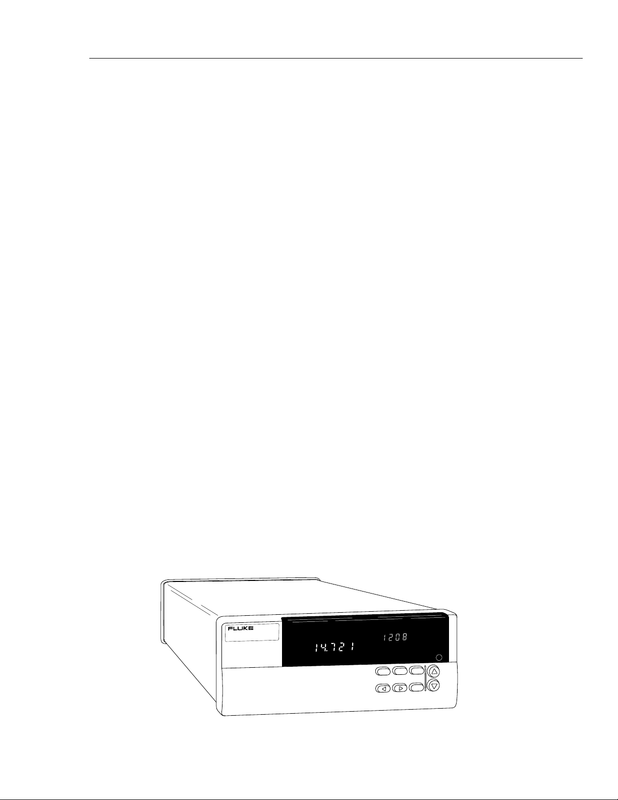
Introduction 1-1.
This Service Manual supports performance testing, calibration, servicing, and
maintenance of the 2640A NetDAQ
units (Figure 1-1). NetDAQ networked data acquisition units are 20-channel front ends
that operate in conjunction with a host computer to form a networked data acquisition
system. The host computer and instruments are interconnected using an Ethernet
network, and the host computer runs the NetDAQ Logger for Windows application to
provide an operating environment for the instruments, including testing and calibration.
The 2640A and 2645A networked data acquisition units are identical in operation and
appearance, and vary only in emphasis: The 2640A emphasizes precision and supports
up to 100 measurements per second, with 5 ½ digits of resolution, .02% accuracy, and
150-volt common mode voltage (300 volts on channels 1 and 11), while the 2645A
emphasizes increased measurement speed supporting up to 1000 measurements per
second, with 4 ½ digits of resolution, .04% accuracy, and 50-volt common mode voltage.
Refer to Table 1-1 for a summary of instrument specifications. For complete instrument
specifications, see “Specifications” later in this chapter.
The instruments measure dc volts, ac volts, ohms, temperature, frequency, and dc
current. Temperature measurements use thermocouples or resistance-temperature
detectors (RTDs). Refer to Table 1-2 for a summary of instrument measurement
capabilities. In addition, there are eight digital input/output lines, one totalizing input,
one external trigger input, one trigger output, and one master alarm output. The
instruments can be ac or dc powered. An RS-232 serial port is supplied for servicing and
maintenance procedures.
™ and 2645A NetDAQ networked data acquisition
1
The term "instrument" is used in this manual to refer to both units. The model number
(2640A or 2645A) is used when discussing characteristics unique to one instrument.
Instrument assemblies are identical except for the A3 Analog/Digital Converter printed
circuit assembly (pca), which is specific to the 2640A (mechanical switching for
measurement signals) and 2645A (solid-state switching for measurement signals).
The instrument is designed for bench-top, field service, and system applications. A dual
vacuum-fluorescent display uses combinations of alphanumeric characters and
descriptive annunciators to provide prompting and measurement information during
setup and operation modes. Some features provided by the instrument are listed in Table
1-3. For additional information regarding instrument features and capabilities, refer to
the NetDAQ Users Manual (PN 942623).
NetDAQ
NETWORKED DATA ACQUISITION UNIT
REM SCAN
MON
V DC
COMM
CH
DIO
ENTER
CAL
ENABLE
MON
Figure 1-1. 2640A/2645A NetDAQ Networked Data Acquisition Units
1-3
Page 20

NetDAQ
Service Manual
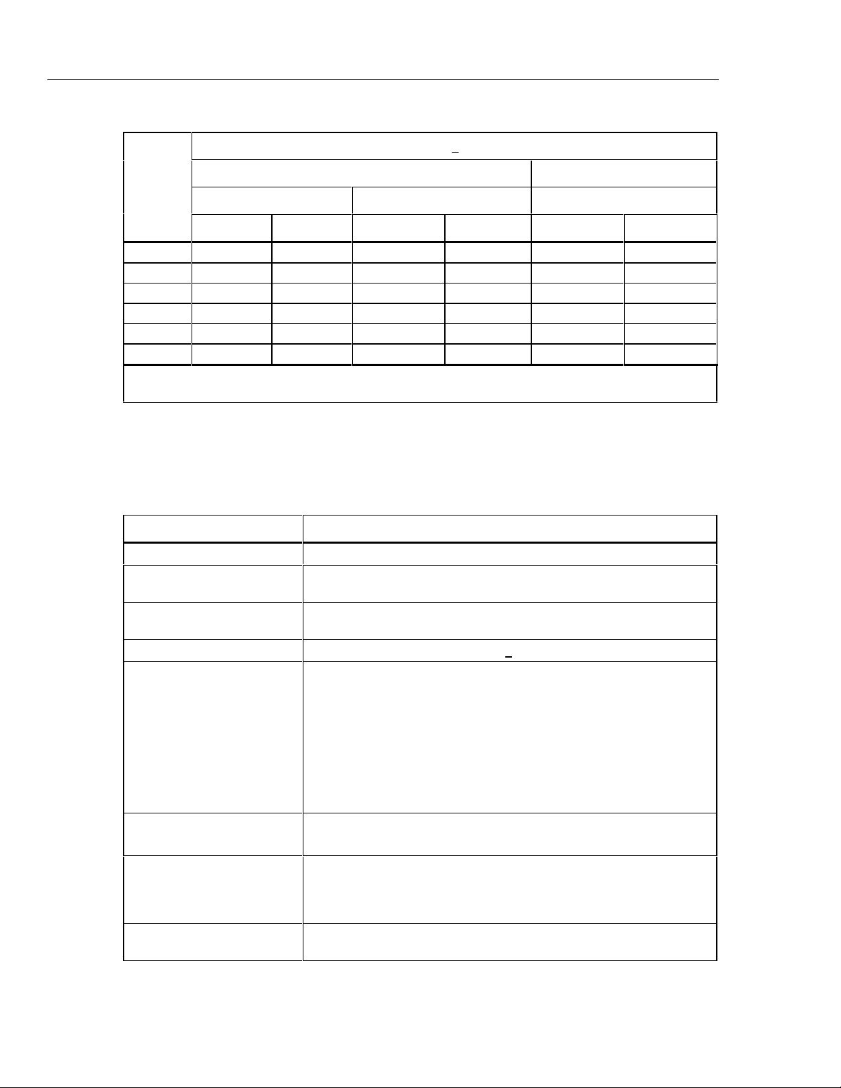
Maximum Normal Mode Voltage 150/300V [1] 50V
Maximum Common Mode
Voltage
Input (Overload) Protection 1600V 300V
Maximum Reading Rates
(Volts DC Only)
Maximum Single Channel Scan
Reading Rates [2]
Volts DC Accuracy (90 day),
1V dc input
Thermocouple Accuracy
(90 day)
Resistance-Temperature
Detectors (RTDs) Resolution
Resistance-Temperature
Detectors (RTDs) Accuracy
Time to Change Functions
(Between V dc, V ac,
Frequency, and Ohms)
[1] The 300V value is for channels 1 and 11 only; the 150V value is for all other channels.
[2] Drift Correction refers to an automatic internal measurement step performed with each
Table 1-1. Summary of 2640A/2645A Specifications
Specification 2640A 2645A
150/300V [1] 50V
143 readings/second
(scanning 20 channels)
80 readings/second
(Drift Correction enabled)
120 readings/second
(Drift Correction disabled)
0.02% 0.04%
0.3°C0.6°C
0.003°C0.03°C
0.12°C0.2°C
6 ms 6 ms
scan to correct for drift due to changes in ambient temperature and humidity.
1000 readings/second
(scanning 20 channels)
250 readings/second
(Drift Correction enabled)
400 readings/second
(Drift Correction disabled)
1-4
Table 1-2. Summary of 2640A/2645A Measurement Capabilities
Capability 2640A 2645A
Volts DC Measurements Ranges: 90 mV
300 mV
3V
30V
150/300V [1]
Autorange
Volts AC Measurements Ranges: 300 mV
3V
30V
150/300V [1]
Autorange
Resistance Measurements Ranges: 300 Ω
3 kΩ
30 kΩ
300 kΩ
3 MΩ
Autorange
Ranges: 90 mV
300 mV
3V
30V
50V
Autorange
Ranges: 300 mV
3V
30V
Autorange
Ranges: 30 kΩ
300 kΩ
3 MΩ
Autorange
Page 21

Introduction and Specification
Table 1-2. Summary of 2640A/2645A Measurement Capabilities (cont)
Capability 2640A 2645A
Introduction
1
Temperature Measurements
(Thermocouple) [2]
Temperature Measurements
(RTD) (Two-wire)
Temperature Measurements
(RTD) (Four-wire)
Frequency Measurements [3] Ranges: Autorange Ranges: Autorange
Amperes DC Measurements [4] Ranges: 4 to 20 mA
[1] 300V range available only on channels 1 and 11.
[2] Open thermocouple detection is supported on a per-channel basis.
[3] Minimum frequency is 20 Hz. Signal strength must be at least 50 mV ac rms.
[4] Shunt resistor required (enter value; default is 10 ohms). The 4 to 20 mA scale displayed as
0% (4 mA) to 100% (20 mA).
Feature Description
Analog Channels 20 (channels 1 to 20)
Computed Channels 10 (channels 21 to 30)
Alarm Limits Two per channel
Mx+B Scaling Any configured channel (1 to 30)
Scan Triggering Interval/External/Alarm Trigger
Channel Monitoring Any configured channel, scanning or not scanning
Setup and Operation Via host computer
Communications Ports Ethernet 10BASE2 and 10BASE-T
Primary Power AC - 107 to 264V ac, 50/60 Hz
Nonvolatile Memory (unaffected by cycling
instrument power)
Permanent Data Storage Via host computer
Real-Time Trend Plotting Via host computer
Thermocouples:
JKRSE
TBCN
RTD R0: 10 to 1010 (None)
RTD R0: 10 to 1010 RTD R0: 10 to 1010
0 to 100 mA
Table 1-3. Summary of 2640A/2645A Features
DC - 9 to 16V dc
Instrument parameters: Base Channel Number,
Line Frequency, Network Type, Socket Port, IP
Address, Baud Rate. (See Chapter 2.)
Thermocouples:
JKRSE
TBCN
Ranges: 4 to 20 mA
0 to 100 mA
1-5
Page 22

NetDAQ
Service Manual
Options and Accessories 1-2.
2640A NetDAQ Instrument
2645A NetDAQ Instrument
264XA-901 NetDAQ
264XA-902 NetDAQ
264XA-902U NetDAQ
264XA-801 Ethernet Card
264XA-802 Parallel-to-LAN Adapter (10BASE2)
80i-410 Clamp-On DC/AC Current Probe
80i-1010 Clamp-On DC/AC Current Probe
2620A-100 I/O connector set, including Universal Input Module, DIGITAL I/O
2620A-101 4-20 mA Current Shunt Strip
942615 NetDAQ Service Manual
Y2641 19-inch Rackmount Kit
Y2643 4-meter Cable Kit
Table 1-4 summarizes the available models, options and accessories, including
measurement transducers, software, connector sets, Ethernet interfaces, cables, and
components.
Table 1-4. Models, Options and Accessories
Model Description
Logger for Windows
Logger for Windows
Logger for Windows
and ALARM/TRIGGER I/O connectors.
(Isolated Network)
(General Network)
Network (Upgrade Kit)
Instrument Connector Set, 2620A-100 1-3.
The 2620A-100 is a complete set of input connectors: one Universal Input Module, one
ALARM/TRIGGER I/O connector, and one DIGITAL I/O connector. Each instrument
comes with a 2620A-100 Instrument Connector Set. The use of additional connector sets
allows quick equipment interface to several wiring setups.
Host Computer Ethernet Interfaces 1-4.
The 264XA-801 is the recommended Ethernet card and the 264XA-802 is the
recommended Parallel-to-LAN Adapter for host computer installations.
Interconnection Cables and Components 1-5.
Cables for equipment interconnection can be purchased as an option or fabricated.
Ethernet interconnection components such as BNC "T" and 50-ohm terminations are
available from any components supplier.
1-6
Page 23

Introduction and Specification
Operating Instructions
Operating Instructions 1-6.
Full operating instructions are provided in the NetDAQ User Manual (PN 942623). Refer
to the User Manual as necessary during the maintenance and repair procedures presented
in this Service Manual.
Organization of the Service Manual 1-7.
This manual focuses on performance tests, calibration procedures, and component-level
repair of the 2640A and 2645A networked data acquisition units. To that end, manual
chapters are often interdependent; effective troubleshooting may require not only
reference to the troubleshooting procedures in Chapter 5, but also some understanding of
the detailed Theory of Operation in Chapter 2 and some tracing of circuit operation in
the Schematic Diagrams presented in Chapter 7.
Often, scanning the table of contents yields an appropriate place to start using the
manual. A comprehensive table of contents is presented at the front of the manual; local
tables of contents are also presented at the beginning of each chapter for ease of
reference. If you know the topic name, the index at the end of the manual is probably a
good place to start.
1
The following descriptions introduce the manual:
Chapter 1 - Introduction and Specifications Introduces the instrument, describing its
features, options, and accessories. This chapter also discusses use of the Service Manual
and the various conventions used in describing the circuitry. Finally, a complete set of
specifications is presented.
Chapter 2 - Theory of Operation This chapter first categorizes the instrument’s
circuitry into functional blocks, with a description of each block’s role in overall
operation. A detailed circuit description is then given for each block. These descriptions
explore operation to the component level and fully support troubleshooting procedures
defined in Chapter 5.
Chapter 3 - General Maintenance Provides maintenance information covering
handling, cleaning, and fuse replacement. Access and reassembly procedures are also
explained in this chapter.
Chapter 4 - Performance Testing and Calibration This chapter provides performance
verification procedures, which relate to the specifications presented in Chapter 1. To
maintain these specifications, a full calibration procedure is also presented.
Chapter 5 - Diagnostic Testing and Troubleshooting The troubleshooting procedures
presented in this chapter rely closely on both the Theory of Operation presented in
Chapter 2, the Schematic Diagrams shown in Chapter 7, and the access information
provided in Chapter 3.
Chapter 6 - List of Replaceable Parts Includes parts lists for all standard assemblies.
Information on how and where to order parts is also provided.
Chapter 7 - Schematic Diagrams Includes schematic Diagrams for all standard and
optional assemblies. A list of mnemonic definitions is also included to aid in identifying
signal name abbreviations.
1-7
Page 24

NetDAQ
Service Manual
Conventions 1-8.
Throughout the manual set, certain notational conventions are used. A summary of these
conventions follows:
• Instrument Reference The term "instrument" is used in this manual to refer to both
the 2640A NetDAQ and 2645A NetDAQ networked data acquisition units. The
model number (2640A or 2645A) is used when discussing characteristics unique to
one instrument.
• Printed Circuit Assembly The term "pca" is used to represent a printed circuit
board and its attached parts.
• Signal Logic Polarity On schematic Diagrams, a signal name followed by a "*"
character is active (or asserted) low. Signals not so marked are active high.
• Circuit Nodes Individual pins or connections on a component are specified with a
dash (-) following the assembly and component reference designators. For example,
pin 19 of U30 on assembly A1 would be A1U30-19.
• Front Panel Interface User Notation For front panel operation, XXX, an
uppercase word or symbol without parentheses indicates a button to be pressed by
the user. Buttons can be pressed in four ways:
1. Press a single button to select a function or operation.
2. Press a combination of buttons, one after the other.
3. Press and hold down a button; then press another button.
4. Press multiple buttons simultaneously.
• Computer Interface User Notation For computer interface operation:
XXX An uppercase word without parentheses identifies a command by name.
<XXX> Angle brackets around all uppercase letters mean press the <XXX> key.
(xxx) A lowercase word in parentheses indicates a keyboard input.
1-8
Specifications 1-9.
Specifications are divided into three sections. The first section contains the combined
specifications that apply equally to both the 2640A and 2645A instruments. The second
section contains specifications that apply only to the 2640A instrument. The third section
contains specifications that apply only to the 2645A instrument.
2640A/2645A Combined Specifications 1-10.
The following specifications apply equally to both the 2640A and 2645A instruments.
The topics include:
• 2640A/2645A General Specifications
• 2640A/2645A Environmental Specifications
• 2640A/2645A Digital I/O and Totalizer Interface
Page 25

Introduction and Specification
Specifications
2640A/2645A General Specifications 1-11.
Table 1-5 provides the general specifications for the 2640A and 2645A instruments.
Table 1-5. 2640A/2645A General Specifications
Specification Characteristic
Channel Capacity 20
I/O Lines Total 12
Size 9.3 cm (3.67 in) high, 21.6 cm (8.5 in) wide, 36.2 cm (14.28 in) deep
Weight Net, 4 kg (8.8 lb.) Shipping, 6.0 kg (13.2 lb.)
Power 107 to 264V ac (no switching required), 45 to 65 Hz, 15 VA maximum
9V dc to 16V dc, 6W maximum. Specifications are for 50 or 60 Hz operation.
If both sources are applied simultaneously, ac voltage is used if it exceeds
approximately 8 times the dc voltage. Automatic switchover occurs between ac
and dc without interruption.
Standards Both instruments comply with:
IEC 1010-1
UL 1244
CSA Bulletin 556B
ANSI/ISA-S8201-1988
CSA C22.2 No. 101.1-92
Vfg. 243/1991 (when shielded cables are used)
FCC-15B, Class B level (when shielded cables are used)
Serial Interface
(RS-232C)
Common Mode
Voltage
Measurement Speed
(Scanning Rates)
Accuracy of Medium
Scanning Rate
Additional error if
“Automatic drift
correction” is turned
off.
Connector: 9 pin male (DB-9P)
Signals: TX, RX, DTR, RTS, GND
Modem Control: full duplex
Baud rates: 4800, 9600, 19200, 38400
Data format: 8 data bits, no parity bit, one stop bit
Flow control: XON/XOFF
Echo: Off
2640A 150V (300V on channels 1 and 11)
2645A 50V dc or 30V ac rms.
2640A
Slow - 6 readings per second
Medium - 48 readings per second (60 Hz)
Fast - 143 readings per second (20 configured channels)
Single Channel - 120 readings per second
2645A
Slow - 54 readings per second (60 Hz)
Medium - 200 readings per second
Fast - 1000 readings per second (20 configured channels)
Single Channel - 400 readings per second
Equal to (Fast Accuracy Rate + Slow Accuracy Rate)/2
If the instrument is fully warmed-up at the time drift correction was disabled, i.e.,
turned on at least 1 hour earlier: 1/10 of the 90-day specification per °C change
in ambient temperature from the temperature when drift correction was disabled.
If the instrument was not fully warmed up at the time of drift correction was
disabled: add an error equal to the 90-day specification for instrument warmup
+1/10 of the 90-day specification per °C change in ambient temperature from the
temperature when drift correction was disabled.
1
1-9
Page 26

NetDAQ
Service Manual
2640A/2645A Environmental Specifications 1-12.
Warmup Time 1 hour to rated specifications -or- 15 minutes if relative humidity
Operating Temperature -10°C to 60°C (14°F to 140°F)
Storage Temperature -40°C to +70°C (-40°F to +158F)
Relative Humidity 90% maximum for -10°C to 28°C (14°F to 82.4°F)
Altitude Operating: 2,000m (6,561 ft) maximum
Vibration 0.7g at 15 Hz
Shock 30g half-sine per Mil-T-28800
Table 1-6 provides a summary of the environmental specifications for the 2640A/2645A.
Table 1-6. Environmental Specifications
Specification Characteristic
(noncondensing) is 50% or less.
75% maximum for 28°C to 35°C (82.4°F to 95°F)
50% maximum for 35°C to 60°C (95°F to 140°F)
(3 MΩ range, reduce humidity rating by 25% for 1 hour warmup.
The 3 MΩ range meets full humidity ratings with 2-hour warmup.)
Non-operating: 12,200m (40,000 ft) maximum
1.3g at 25 Hz
3g at 55 Hz
Bench handling per Mil-T-28800
2640A/2645A Input/Output Capabilities 1-13.
The following specifications include the input/output functions, including the Digital
I/O, Trigger Out, Trigger In, and Master Alarm output.
Digital I/O 1-14.
Table 1-7 provides a summary of the Digital I/O specifications for the 8 Digital I/O lines
(0 to 7). Digital I/O is located on the DIGITAL I/O connector, terminals 0 to 7, and
GND.
Table 1-7. 2640A/2645A DIGITAL I/O Specification
Specification Characteristic
Maximum Input Voltage 30V
Minimum Input Voltage -4V
Isolation None (dc coupled)
Threshold 1.4V
Hysteresis 500 mV
Specification Characteristic
Output Voltage - TTL Logical Zero 0.8V maximum for an Iout of -1.0 mA (1 LSTTL load)
Output Voltage - TTL Logical One 3.8V minimum for an Iout of 0.05 mA (1 LSTTL load)
Output Voltage - Non-TTL Load Zero 1.8V maximum for an Iout of -20 mA
Output Voltage - Non-TTL Load One 3.25V maximum for an Iout of -50 mA
1-10
Page 27

Introduction and Specification
Specifications
Trigger In 1-15.
Table 1-8 provides a summary of the Trigger In specifications. The Trigger In input is
located on the ALARM/TRIGGER I/O connector, terminals TI and GND.
Table 1-8. 2640A/2645A Trigger In (TI) Specification
Specification Characteristic
Logical High - Trigger not set Minimum: 2.0V
Maximum: 7.0V
Logical Low - Trigger set Minimum: -0.6V
Maximum: +0.8 V
Compatibility TTL or Contact Closure
Isolation None (dc coupled)
Minimum Pulse Width 5 µs
Maximum Frequency Nominal 400 Hz
Repeatability 3 ms
Trigger Out 1-16.
1
Table 1-9 provides a summary of the Trigger Out specifications. The Trigger Out output
is located on the ALARM/TRIGGER I/O connector, terminals TO and GND.
Table 1-9. 2640A/2645A Trigger Out (TO) Specification
Specification Characteristic
TTL Logical Zero - Trigger Out Set 0.8V maximum for an Iout of -1.0 mA (1 LSTTL load)
TTL Logical One - Trigger Out Not Set 3.8V minimum for an Iout of 0.05 mA (1 LSTTL load)
Non-TTL Logical Zero - Trigger Out Set 1.8V maximum for an Iout of -20 mA
Non-TTL Logical One - Trigger Out Not Set 3.25V maximum for an Iout of -50 mA
Pulse Duration (Logic Low) 125 µs
Isolation None
Master Alarm 1-17.
Table 1-10 provides a summary of the Master Alarm specifications. The Master Alarm
output is located on the ALARM/TRIGGER I/O connector, terminals MA and GND.
Table 1-10. 2640A/2645A Master Alarm (MA) Specification
Specification Characteristic
TTL Logical Zero - Master Alarm Set 0.8V maximum for an Iout of -1.0 mA (1 LSTTL load)
TTL Logical One - Master Alarm Not Set 3.8V minimum for an Iout of 0.05 mA (1 LSTTL load)
Non-TTL Logical Zero - Master Alarm Set 1.8V maximum for an Iout of -20 mA
Non-TTL Logical One - Master Alarm Not Set 3.25V maximum for an Iout of -50 mA
Isolation None
1-11
Page 28

NetDAQ
Service Manual
2640A/2645A Totalizer 1-18.
Maximum Input Voltage 30V
Minimum Input Voltage -4V
Minimum Peak Voltage 2V
Isolation None (dc coupled)
Threshold 1.4V
Hysteresis 500 mV
Input Debouncing None or 1.75 ms (selectable)
Maximum Transition Rate 5 kHz (Debounce disabled)
Maximum Count 4,294,967,295
Table 1-11 provides a summary of the Totalizer specifications. The Totalizer input is
located on the DIGITAL I/O connector, terminals Σ and GND.
Table 1-11. 2640A/2645A Totalizer Specification
Specification Characteristic
500 Hz (Debounce enabled)
2640A/2645A Real-Time Clock and Calendar 1-19.
Table 1-12 provides a summary of the battery powered real-time clock and calendar.
Table 1-12. 2640A/2645A Real-Time Clock and Calendar
Specification Characteristic
Accuracy 1 minute per month for 0°C to 50°C range
Battery Life >15 unpowered instrument years for 0°C to 28°C (32°F to 82.4°F).
>6 unpowered instrument years for 0°C to 50°C (32°F to 122°F).
>4 unpowered instrument years for 50°C to 70°C (122°F to 158°F).
1-12
Page 29

Introduction and Specification
Specifications
2640A Specifications 1-20.
This section includes specifications specific to the 2640A instrument by measurement
function.
2640A DC Voltage Measurement Specifications 1-21.
Tables 1-13 to 1-15 provide 2640A specifications for the dc voltage measurement
function.
Table 1-13. 2640A DC Voltage General Specifications
Specification Characteristic
Input Impedance 100 MΩ in parallel with 300 pF maximum for ranges <=3V
10 MΩ in parallel with 100 pF maximum for ranges >3V
Normal Mode Rejection 50 dB minimum at 50 Hz/60 Hz +0.1%, Slow Rate
Common Mode Rejection 120 dB minimum at dc, 50 Hz/60 Hz +0.1%, 1 kΩ imbalance, Slow
Rate
80 dB minimum at dc, 50 Hz/60 Hz +0.1%, 1 kΩ imbalance, Medium
and Fast Rates
Channel-to-Channel Crosstalk 120 dB minimum Slow Rate (e.g., 30V dc on channel 1 may cause a
30 µV error on channel 2)
100 dB minimum Medium and Fast Rates (e.g., 1V dc on channel 1
may cause a 10 µV error on channel 2)
Temperature Coefficient For % input: Add 1/10th the 90-day specification per °C above 28 °C
or below 18 °C
For floor error (V): Add 1/20th the 90-day specification per °C above
28 °C or below 18 °C
Maximum Input Voltage The lesser voltage of:
300V from any terminal on channels 1 and 11 to earth;
150V from any terminal on channels 2 through 10, and 12 through 20
to earth;
300V from any terminal on channels 1 and 11 to any other terminal;
150V from any terminal on channels 2 through 10, and 12 through 20
to any other input terminal
1
Table 1-14. 2640A DC Voltage Range and Resolution Specifications
Resolution
Range
90 mV 0.3 µV1 µV
300 mV 1 µV3 µV
3V 10 µV30 µV
30V 100 µV 300 µV
150V/300V 1 mV 3 mV
Note 300V range applies to channels 1 and 11 only.
Slow Fast
1-13
Page 30
NetDAQ
Service Manual
90 mV .01%+7 µV .01%+17 µV .013%+8 µV .013%+18 µV .042%+18.2 µV .042%+44.2 µV
300 mV .01%+15 µV .01%+30 µV .013%+17 µV .013%+35 µV .042%+39 µV .042%+78 µV
750 mV* .01%+40 µV .01%+70 µV .013%+50 µV .013%+80 µV .042%+104 µV .042%+182 µV
3V .01%+0.1 mV .01%+0.2 mV .013%+0.15 mV .013%+0.2 mV .042%+0.26 mV .042%+0.52 mV
30V .01%+1.5 mV .02%+3 mV .013%+1.7 mV .026%+3.5 mV .042%+3.9 mV .084%+7.8 mV
150/300V** .01%+15 mV .04%+30 mV .013%+17 mV .052%+35 mV .042%+39 mV .168%+78 mV
* The 750 mV range is used internally to the instrument and not user selectable.
** 300V range applies to channels 1 and 11 only.
2640A AC Voltage Measurement Specifications 1-22.
Range
Table 1-15. 2640A DC Voltage Accuracy Specifications
Accuracy, 3σ + (% input + V)
18°C to 28°C-10°C to 60°C
90 Day 1 Year 1 Year
Slow Fast Slow Fast Slow Fast
Tables 1-16 to 1-18 provide 2640A specifications for the ac voltage measurement
function.
Table 1-16. 2640A AC Voltage General Specifications
Specification Characteristic
Input Impedance 1 MΩ in parallel with 100 pF
Maximum Crest Factor 3.0 Maximum
2.0 for rated accuracy
Crest Factor Error For nonsinusoidal input signals with crest factors between 2 and 3 and
pulse widths >=100 µs, add 0.2% to the accuracy specifications.
Common Mode Rejection 80 dB minimum at dc, 50 Hz/60 Hz +0.1%, 1 kΩ imbalance, Slow Rate
Maximum Input Voltage The lesser voltage of:
300V ac rms from any terminal on channels 1 and 11 to earth.
150V ac rms from any terminal on channels 2 through 10, and 12
through 20 to earth.
300V ac rms from any terminal on channels 1 and 11 to any other
terminal.
150V ac rms from any terminal on channels 2 through 10 and 12
through 20 to any other input terminal.
Maximum Volt-Hertz Product 2x10⁶ Volt-Hertz product on any range, normal mode input.
6
1x10
Volt-Hertz product on any range, common mode input.
Temperature Coefficient Linear interpolation between 2 applicable points for temperatures
between 28°C and 60°C, or -10°C and 18°C, e.g., if the applicable
specification at 28°C is 2% and the specification at 60°C is 3%, then the
specification at 40°C is (3%-2%)x(40-28)/(60-28)+2%=2.375%.
DC Component Error The presence of a dc voltage will cause an indeterminate error in the
reading of the ac voltage on the input.
1-14
Page 31

Introduction and Specification
Table 1-17. 2640A AC Voltage Range and Resolution Specifications
Specifications
1
Range
Slow Fast
Full Scale +30,000 +3,000
300 mV 10 µV 100 µV 20 mV
3V 100 µV 1 mV 200 mV
30V 1 mV 10 mV 2V
150/300V 10 mV 100 mV 20V
Note 300V range applies to channels 1 and 11 only.
Table 1-18. 2640A AC Voltage Accuracy Specifications
Range Frequency 18°C to 28°C-10°C to 60°C
300 mV 20 to 50 Hz 3%+.25 mV 6%+.5 mV 3.5%+.25 mV 7%+.5 mV
50 to 150 Hz 0.4%+.25 mV 1%+.5 mV 0.5%+.25 mV 1.5%+.5 mV
150 Hz to 10 kHz 0.3%+.25 mV 1%+.5 mV 0.4%+.25 mV 1.5%+.5 mV
10 kHz to 20 kHz 0.4%+.25 mV 1%+.5 mV 0.7%+.25 mV 1.5%+.5 mV
20 kHz to 50 kHz 2%+.3 mV 3%+.5 mV 3%+.3 mV 4%+.5 mV
50 kHz to 100 kHz 5%+.5 mV 5%+1 mV 7%+.5 mV 8%+1 mV
3V 20 to 50 Hz 3%+2.5 mV 6%+5 mV 3.5%+2.5 mV 7%+5 mV
50 to 150 Hz 0.4%+2.5 mV 1%+5 mV 0.5%+2.5 mV 1.2%+5 mV
150 Hz to 10 kHz 0.3%+2.5 mV 1%+5 mV 0.4%+2.5 mV 1.2%+5 mV
10 kHz to 20 kHz 0.4%+2.5 mV 1%+5 mV 0.5%+2.5 mV 1.2%+5 mV
20 kHz to 50 kHz 1%+3 mV 1.5%+6 mV 1.5%+3 mV 2%+6 mV
50 kHz to 100 kHz 2%+5 mV 3%+10 mV 3%+5 mV 4%+10 mV
30V 20 to 50 Hz 3%+25 mV 6%+50 mV 3.5%+25 mV 7%+50 mV
50 to 150 Hz 0.4%+25 mV 1%+50 mV 0.5%+25 mV 1.2%+40 mV
150 Hz to 10 kHz 0.3%+25 mV 1%+50 mV 0.5%+25 mV 1.2%+40 mV
10 kHz to 20 kHz 0.4%+25 mV 1%+50 mV 0.5%+25 mV 1.2%+40 mV
20 kHz to 50 kHz 1%+30 mV 1.5%+60 mV 1%+30 mV 2%+50 mV
50 kHz to 100 kHz, V<20V 2%+50 mV 3%+100 mV 2.5%+50 mV 4%+100 mV
150/300V 20 to 50 Hz 3%+.25V 6%+.5V 3.5%+.25V 7%+.5V
50 to 150 Hz 0.4%+.25V 1%+.5V 0.5%+.25V 1.2%+.4V
150 Hz to 2 kHz
Vx Hz<2 x10
2 kHz to 20 kHz, V<100V 0.4%+.25V 1.6%+.5V 0.5%+.25V 1.8%+.4V
20 kHz to 50 kHz, V<40V 1%+.30V 2.0%+.6V 1.2%+.30V 2.5%+.5V
[1] Sinewave inputs>6% of scale and signals with crest factors <2.
6
Resolution
1 Year Accuracy + (%input + V) [1]
Slow Fast Slow Fast
0.3%+.25V 1.2%+.5V 0.5%+.25V 1.4%+.4V
Minimum Input for
Rate Accuracy
1-15
Page 32

NetDAQ
Service Manual
2640A Four-Wire Resistance Measurement Specifications 1-23.
Temperature Coefficient Add 1/10th the 90 day specification per °C
Tables 1-19 to 1-21 provide 2640A specifications for the four-wire resistance
measurement function. The four-wire measurements use 2 input channels a decade apart,
e.g., channels 4 and 14.
Table 1-19. 2640A Four-Wire Resistance Temperature Coefficient
Specification Characteristic
above 28°C or below 18°C.
Table 1-20. 2640A Four-Wire Resistance Range and Resolution Specifications
Resolution
Range Slow Fast
300Ω 1 mΩ 3mΩ 1 mA 300 mV 3.5V
3 kΩ 10 mΩ 30 mΩ 100 µA 300 mV 3.5V
30 kΩ 100 mΩ 300 mΩ 10 µA 300 mV 3.5V
300 kΩ 1Ω 3Ω 10 µA 3.0V 3.5V
3 MΩ 10Ω 30Ω 1 µA 3.0V 3.5V
Table 1-21. 2640A Four-Wire Resistance Accuracy Specifications
Range
300Ω . 015%+20 mΩ .02%+80 mΩ .02%+50 mΩ .02%+120 mΩ .084%+126 mΩ .084%+336 mΩ
3 kΩ .02%+.3Ω .02%+.8Ω .02%+.5Ω .02%+1.2Ω .084%+1.26Ω .084%+3.36Ω
30 kΩ .03%+3Ω .04%+10Ω .03%+5Ω .04%+15Ω .126%+12.6Ω .168%+42Ω
300 kΩ .1%+40Ω .2%+100Ω .1%+60Ω .2%+150Ω .42%+168Ω .84%+420Ω
3 MΩ [1] .25%+800Ω .5%+10 kΩ .25%+1 kΩ .5%+1.5 kΩ 1.05%+3.36 kΩ 2.1%+4.2 kΩ
[1] The 3 MΩ range is susceptible to the abs orpt i on of humidity under extreme condi t i ons. If the instrument i s
operated normally within its specified temperature-humidi ty range, the 3 MΩ range meets i t s accuracy specifi cations.
However, if the instrument is “soaked” at 50°C, 90% relati ve humidity, the 3 MΩ range may require 1 hour of “dry-out”
time at 25°C, <40% relative humidity for eac h hour of soak time in order to achiev e i ts specified accurac y.
90 Day 1 Year 1 Year
Slow Fast Slow Fast Slow Fast
Current Full Scale Maximum Voltage
Applied Voltage Applied by Instrument
Accuracy, 3σ + (% input + V)
18°C to 28°C-10°C to 60°C
1-16
2640A Two-Wire Resistance Measurement Specifications 1-24.
The 2640A specifications for the two-wire resistance measurement function is based on
the four-wire resistance measurement specification (above) except you add a nominal
5-ohm (10-ohm maximum) positive offset. This value varies for each channel and with
temperature
(nominal +1%/ºC).
Page 33

Introduction and Specification
Specifications
2640A Four-Wire RTD per ITS-1990 Measurement Specifications 1-25.
Tables 1-22 and 1-23 provide 2640A specifications for the four-wire ResistanceTemperature Detector (RTD) measurement function. The four-wire measurements use 2
input channels a decade apart, e.g., channels 4 and 14.
Table 1-22. 2640A Four-Wire RTD Temperature Coefficient
Specification Characteristic
Temperature Coefficient To calculate RTD accuracy for temperatures between 28°C and 60°C, or
-10°C and 18°C, use a linear interpolation between the two applicable
points. For example, if the applicable specification at 28°C is 0.2 and the
specification at 60°C is 0.75, then the specification at 40°C is =(.75-
.2)x(40-28)/(60-28)+.2=0.406.
Table 1-23. 2640A Four-Wire RTD Specifications
Accuracy, 3σ
1
Resolution 90 Day
Temperature
Slow Fast Slow Fast Slow Slow Fast
-200°C 0.003°C 0.007°C0.06°C0.16°C0.09°C0.33°C0.63°C
0°C 0.003°C 0.007°C0.09°C0.20°C0.13°C0.53°C0.86°C
100°C 0.003°C 0.007°C0.10°C0.23°C0.16°C0.63°C0.97°C
300°C 0.003°C 0.007°C0.14°C0.30°C0.21°C0.83°C1.20°C
600°C 0.003°C 0.007°C0.19°C0.53°C0.30°C1.20°C1.60°C
18°C to 28°C
1 Year
18°C to 28°C
1 Year
-10°C to 60°C
2640A Two-Wire RTD per ITS-1990 Measurement Specifications 1-26.
The 2640A specifications for the two-wire Resistance-Temperature Detector (RTD)
measurement function is based on the four-wire RTD measurement specification (above)
except you add a nominal 5-ohm (approximately 13°C) positive offset. This value varies
for each channel and temperature gradient (nominal +1%/ºC). Also note that the
resistance of the RTD wiring adds directly to the error. After 100 million operations of a
measurement channel, the offset will increase at an indeterminate rate.
1-17
Page 34

NetDAQ
Service Manual
2640A Thermocouple per ITS-1990 Measurement Specifications 1-27.
Input Impedance 100 MΩ minimum in parallel with 300 pF
Open Thermocouple Detect Operates by injecting a small ac signal into the
Temperature Coefficient To calculate Thermocouple accuracy for
Tables 1-24 to 1-25 provide 2640A specifications for the thermocouple measurement
function per ITS-1990.
Table 1-24. 2640A Thermocouple General Specifications
Specification Characteristic
input after each measurement. A
thermocouple resistance greater than 1k to
10k is detected as an open input.
temperatures between 28°C and 60°C, or
-10°C and 18°C, use a linear interpolation
between the two applicable points. For
example, if the applicable specification at
28°C is 0.6 and the specification at 60°C is
1.1, then the specification at 40°C is =(1.1-
0.6)x(40-28)/(60-28)+0.6=0.7875.
Table 1-25. 2640A Thermocouple Specifications
Accuracy + °C
Thermocouple Resolution 18°C to 28°C-10°C to 60°C
90 Day 1 Year 1 Year
Type Temperature °C Slow Slow Fast Slow Fast
J -100 to 80 .03 0.45 0.50 0.80 0.60 0.80
80 to 230 .02 0.35 0.50 0.70 0.60 0.80
230 to 760 .02 0.40 0.50 0.70 0.80 0.90
K -100 to -25 .04 0.55 0.60 0.90 0.70 1.00
-25 to 120 .03 0.40 0.50 0.80 0.60 0.90
120 to 800 .03 0.50 0.65 0.90 1.00 1.20
800 to 1372 .03 0.70 1.00 1.30 1.60 1.90
N -100 to -25 .05 0.65 0.75 1.20 0.80 1.30
-25 to 120 .05 0.55 0.60 1.00 0.70 1.10
120 to 1000 .04 0.45 0.60 0.90 1.00 1.20
1000 to 1300 .03 0.55 0.75 1.00 1.20 1.50
E -100 to -25 .03 0.45 0.50 0.80 0.60 0.80
-25 to 20 .02 0.35 0.40 0.60 0.50 0.70
20 to 600 .02 0.30 0.40 0.60 0.50 0.80
600 to 1000 .02 0.40 0.50 0.70 0.90 1.00
T -100 to 0 .04 0.60 0.65 1.00 0.70 1.10
0 to 150 .03 0.40 0.50 0.80 0.60 0.90
150 to 400 .02 0.30 0.40 0.60 0.60 0.80
1-18
Page 35

Introduction and Specification
Table 1-25. 2640A Thermocouple Specifications (cont)
Accuracy + °C
Thermocouple Resolution 18°C to 28°C-10°C to 60°C
90 Day 1 Year 1 Year
Type Temperature °C Slow Slow Fast Slow Fast
R 250 to 600 0.1 0.90 1.00 2.10 1.20 2.20
600 to 1500 0.1 0.80 0.90 1.80 1.30 2.00
1500 to 1767 0.1 0.85 0.85 1.90 1.70 2.50
S 250 to 1000 0.1 0.95 1.10 2.30 1.30 2.40
1000 to 1400 0.1 0.80 1.00 1.90 1.40 2.30
1400 to 1767 0.1 1.00 1.30 2.20 1.80 2.80
B 600 to 900 0.2 1.20 1.40 3.10 1.50 3.20
900 to 1200 0.2 0.90 1.00 2.20 1.20 2.40
1200 to 1820 0.1 0.75 1.00 1.90 1.30 2.20
C 0 to 150 0.2 0.80 0.90 1.60 1.00 1.70
150 to 650 0.1 0.65 0.75 1 .40 1.00 1.50
650 to 1000 .05 0.65 0.85 1.40 1.20 1.80
1000 to 1800 .05 1.00 1.30 2.10 2.10 2.80
1800 to 2316 .05 1.60 2.10 3.20 3.40 4.60
Specifications
1
2640A Frequency Measurement Specifications 1-28.
Tables 1-26 to 1-27 provide 2640A specifications for the frequency measurement
function.
Table 1-26. 2640A Frequency Accuracy Specifications
Frequency Measurement Accuracy, 1 Year, -10°C to 60°C
Range Resolution Accuracy + (% input + Hz)
Slow Fast Slow Fast
15 Hz to 900 Hz 0.01 Hz 0.1 Hz 0.05%+0.02 Hz 0.05%+0.2 Hz
900 Hz to 9 kHz 0.1 Hz 1 Hz 0.05%+0.1 Hz 0.05%+1 Hz
9 kHz to 90 kHz 1 Hz 10 Hz 0.05%+1 Hz 0.05%+10 Hz
90 kHz to 900 kHz 10 Hz 100 Hz 0.05%+10 Hz 0.05%+100 Hz
1 MHz 100 Hz 1 kHz 0.05%+100 Hz 0.05%+1 kHz
1-19
Page 36

NetDAQ
Service Manual
15 Hz to 70 kHz 100 mV ac rms V<150/300Vrms [1] and Vx Hz<2x10⁶)
70 kHz to 100 kHz 100 mV ac rms 20V ac rms
100 kHz to 200 kHz 150 mV ac rms 10V ac rms
200 kHz to 300 kHz 150 mV ac rms 7V ac rms
300 kHz to 1 MHz Linearly increasing from 150 mV ac
[1] 300V range applies to channels 1 and 11 only.
2645A Specifications 1-29.
Table 1-27. 2640A Frequency Sensitivity Specifications
Frequency Measurement Sensitivity (Sinewave)
Frequency Range Minimum Signal Maximum Signal
Linearly decreasing from 7 V ac rms
rms at 300 kHz to 2 V ac rms at 1 MHz
at 300 kHz to 2 V ac rms at 1 MHz
This section includes specifications specific to the 2645A instrument by measurement
function.
2645A DC Voltage Measurement Specifications 1-30.
Tables 1-28 to 1-30 provide 2645A specifications for the dc voltage measurement
function.
Table 1-28. 2645A DC Voltage General Specifications
Specification Characteristic
Input Impedance 100 MΩ in parallel with 300 pF maximum for ranges <=3V
10 MΩ in parallel with 100 pF maximum for ranges >3V
Normal Mode Rejection 50 dB minimum at 50 Hz/60 Hz +0.1%, Slow Rate
Common Mode Rejection 120 dB minimum at dc, 50 Hz/60 Hz +0.1%, 1 kΩ imbalance, Slow Rate
80 dB minimum at dc, 60 dB at 50 Hz/60 Hz +0.1%, 1 kΩ imbalance,
Medium and Fast Rates
Channel-to-Channel
Crosstalk
Temperature Coefficient For % input: Add 1/10th the 90-day specification per °C above 28°C or
Maximum Input Voltage The lesser voltage of:
120 dB minimum Slow Rate (e.g., 30V dc on channel 1 may cause a 30 µV
error on channel 2)
80 dB minimum Medium and Fast Rates (e.g., 1V dc on channel 1 may
cause a 10 µV error on channel 2)
below 18°C.
For floor error (V): Add 1/20th the 90-day specification per °C above 28°C
or below 18°C.
50V dc or 30V ac rms from any input terminal to earth
-or-
50V dc or 30V ac rms from any input terminal to any other input terminal
1-20
Page 37

Introduction and Specification
Specifications
Table 1-29. 2645A DC Voltage Resolution and Repeatability Specifications
Resolution
Range
90 mV 3 µV6 µV
300 mV 1 µV3 µV
3V 10 µV30 µV
30V 100 µV 300 µV
50V 1 mV 3 mV
Table 1-30. 2645A DC Voltage Accuracy Specifications
Range
90 mV .01%+20 µV .01%+50 µV .013%+23 µV .013%+50 µV .042%+52 µV .042%+130 µV
300 mV .01%+40 µV .01%+90 µV .013%+49 µV .013%+93 µV .042%+104 µV .042%+234 µV
750 mV* .01%+90 µV .01%+200 µV .013%+105 µV .013%+220 µV .042%+273 µV .042%+520 µV
3V .01%+.3 mV .01%+.6 mV .013%+.38 mV .013%+.64 mV .042%+.78 mV .042%+1.56 mV
30V .01%+4 mV .02%+8 mV .013%+4.9 mV .026%+9.5 mV .042%+10.6 mV .084%+20.3 mV
50V .01%+30 mV .04%+60 mV .013%+40 mV .052%+64 mV .042%+78 mV .168%+156 mV
* The 750 mV range is used internally to the instrument and not user selectable.
90 Day 1 Year 1 Year
Slow Fast Slow Fast Slow Fast
Slow Fast
Accuracy, 3σ + (% input + V)
18°C to 28°C-10°C to 60°C
1
2645A AC Voltage Measurement Specifications 1-31.
Tables 1-31 to 1-33 provide 2645A specifications for the ac voltage function.
Table 1-31. 2645A AC Voltage General Specifications
Specification Characteristic
Input Impedance 1 MΩ in parallel with 100 pF
Maximum Crest Factor 3.0 maximum; 2.0 for rated accuracy
Crest Factor Error For nonsinusoidal input signals with crest factors between 2 and 3 and
pulse widths >=100 µs, add 0.2% to the accuracy specifications.
Common Mode Rejection 80 dB minimum at dc, 50 Hz/60 Hz +0.1%, 1 kΩ imbalance, Slow Rate
Maximum Input Voltage The lesser voltage of:
30V ac rms from any input terminal to earth.
30V ac rms from any terminal input to any other input terminal.
Maximum Volt-Hertz Product 2x10⁶ Volt-Hertz product on any range, normal mode input.
Temperature Coefficient Linear interpolation between 2 applicable points for temperatures
DC Component Error The presence of a dc voltage will cause an indeterminate error in the
6
Volt-Hertz product on any range, common mode input.
1x10
between 28°C and 60°C, or -10°C and 18°C, e.g., if the applicable
specification at 28°C is 2% and the specification at 60°C is 3%, then the
specification at 40°C is (3%-2%)x(40-28)/(60-28)+2%=2.375%.
reading of the ac voltage on the input.
1-21
Page 38

NetDAQ
Service Manual
Table 1-32. 2645A AC Voltage Range and Resolution Specifications
Range
Slow Fast
Full Scale +30,000 +3,000
300 mV 10 µV 100 µV 20 mV
3V 100 µV 1 mV 200 mV
30V 1 mV 10 mV 2V
Table 1-33. 2645A AC Voltage Accuracy Specifications
Range Frequency 18°C to 28°C-10°C to 60°C
300 mV 20 to 50 Hz 3%+.25 mV 6%+.5 mV 3.5%+.25 mV 7%+.5 mV
50 to 150 Hz 0.4%+.25 mV 0.8%+.5 mV 0.5%+.25 mV 1%+.5 mV
150 Hz to 10 kHz 0.3%+.25 mV 0.8%+.5 mV 0.4%+.25 mV 1%+.5 mV
10 kHz to 20 kHz 0.4%+.25 mV 1%+.5 mV 0.7%+.25 mV 1.5%+.5 mV
20 kHz to 50 kHz 2%+.3 mV 3%+.5 mV 3%+.3 mV 4%+.5 mV
50 kHz to 100 kHz 5%+.5 mV 5%+1 mV 7%+.5 mV 8%+1 mV
3V 20 to 50 Hz 3%+2.5 mV 6%+5 mV 3.5%+2.5 mV 7%+5 mV
50 to 150 Hz 0.4%+2.5 mV 0.8%+5 mV 0.5%+2.5 mV 1%+5 mV
150 Hz to 10 kHz 0.3%+2.5 mV 0.6%+5 mV 0.4%+2.5 mV 1%+5 mV
10 kHz to 20 kHz 0.4%+2.5 mV 0.8%+5 mV 0.5%+2.5 mV 1%+5 mV
20 kHz to 50 kHz 1%+3 mV 1.5%+6 mV 1.5%+3 mV 2%+6 mV
50 kHz to 100 kHz 2%+5 mV 3%+10 mV 3%+5 mV 4%+10 mV
30V 20 to 50 Hz 3%+25 mV 6%+50 mV 3.5%+25 mV 7%+50 mV
50 to 150 Hz 0.4%+25 mV 0.8%+50 mV 1.2%+25 mV 1.3%+40 mV
150 Hz to 10 kHz 0.4%+25 mV 0.8%+50 mV 1.2%+25 mV 1.3%+40 mV
10 kHz to 20 kHz 0.4%+25 mV 0.8%+50 mV 1.2%+25 mV 1.3%+40 mV
20 kHz to 50 kHz 1%+30 mV 1.5%+60 mV 1.2%+30 mV 2%+50 mV
50 kHz to 100 kHz, V<20V 2%+50 mV 3%+100 mV 2.5%+50 mV 4%+100 mV
[1] Sinewave inputs>6% of scale and signals with crest factors <2.
Resolution
1 Year Accuracy + (%input + V) [1]
Slow Fast Slow Fast
Minimum Input for
Rate Accuracy
1-22
Page 39

Introduction and Specification
Specifications
2645A Four-Wire Resistance Measurement Specifications 1-32.
Tables 1-34 to 1-36 provide 2645A specifications for the four-wire resistance
measurement function. The four-wire measurements use 2 input channels a decade apart,
e.g., channels 4 and 14.
Table 1-34. 2645A Four-Wire Resistance Temperature Coefficient
Specification Characteristic
1
Temperature
Coefficient
Table 1-35. 2645A Four-Wire Resistance Range and Resolution Specifications
Resolution
Range
300Ω 10 mΩ 30 mΩ 1 mA 300 mV 3.5V
3 kΩ 100 mΩ 300 mΩ 100 µA 300 mV 3.5V
30 kΩ 1Ω 3Ω 10 µA 300 mV 3.5V
300 kΩ 10Ω 30Ω 10 µA 3.0V 3.5V
3 MΩ 100Ω 300Ω 1 µA 3.0V 3.5V
Range
300Ω .02% +60 m Ω .02%+.1Ω .02%+.1Ω .02%+.2Ω .084%+.25Ω .084%+.42Ω
3 kΩ .02%+.6Ω .02%+2Ω .02%+1Ω .02%+3Ω .084%+2.5Ω .084%+8.4Ω
30 kΩ .02%+6Ω .2%+200Ω .02%+10Ω .2%+300Ω .084%+25Ω .84%+840Ω
300 kΩ .5%+80Ω 1%+2 kΩ .5%+150Ω 1%+3 kΩ 2.1%+336Ω 4.2%+8.4 kΩ
3 MΩ 1.3%+1 k Ω 2%+120 kΩ 1.3%+2 kΩ 2%+200 kΩ 5.46% +4. 2 kΩ 8.4%+200 kΩ
Slow Fast
Table 1-36. 2645A Four-Wire Resistance Accuracy Specifications
Slow Fast Slow Fast Slow Fast
Add 1/10th the 90 day specification per °C above 28°C or below 18°C.
Current Full Scale Maximum Voltage
Applied Voltage Applied by Instrument
Accuracy, 3σ + (% input + Ω)
18°C to 28°C-10°C to 60°C
90 Day 1 Year 1 Year
2645A Two-Wire Resistance Measurement Specifications 1-33.
The 2645A specifications for the two-wire resistance measurement function is based on
the four-wire resistance measurement specification (above) except you add a 700 to 1000
ohm positive offset. This value varies for each channel and temperature gradient
(nominal +1%/ºC).
1-23
Page 40

NetDAQ
Service Manual
2645A Four-Wire RTD per ITS-1990 Measurement Specifications 1-34.
Temperature Coefficient To calculate RTD accuracy for temperatures between 28°C and
Tables 1-37 and 1-38 provide 2645A specifications for the four-wire ResistanceTemperature Detector (RTD) measurement function. The four-wire measurements use 2
input channels a decade apart, e.g., channels 4 and 14. There is no two-wire RTD
capability for the 2645A.
Table 1-37. 2645A Four-Wire RTD Temperature Coefficient
Specification Characteristic
60°C, or -10°C and 18°C, use a linear interpolation between the two
applicable points. For example, if the applicable specification at
28°C is 0.2 and the specifications at 60°C is 0.75, then the
specification at 40°C =(.75-.2)x(40-28)/(60-28)+.2=.406.
Table 1-38. 2645A Four-Wire RTD Specifications
Accuracy, 3σ
Temperature Resolution
Slow Fast Slow Fast Slow Slow Fast
-200°C0.03°C0.06°C0.16°C0.25°C0.25°C0.62°C1.10°C
0°C0.03°C0.06°C0.20°C0.31°C0.31°C0.85°C1.30°C
100°C0.03°C0.06°C0.23°C0.34°C0.34°C0.95°C1.40°C
300°C0.03°C0.06°C0.30°C0.41°C0.41°C1.18°C1.70°C
600°C0.03°C0.06°C0.53°C0.63°C0.63°C1.62°C2.12°C
90 Day
18°C to 28°C
1 Year
18°C to 28°C
1 Year
-10°C to 60°C
2645A Thermocouple per ITS-1990 Measurement Specifications 1-35.
Tables 1-39 to 1-40 provide 2645A specifications for the thermocouple measurement
function per ITS-1990.
Table 1-39. 2645A Thermocouple General Specifications
Specification Characteristic
Input Impedance 100 MΩ minimum in parallel with 300 pF
Open Thermocouple Detect Operates by injecting a small ac signal into the input after each
measurement. A thermocouple resistance greater than 1 k to 10k is
detected as an open input.
Temperature Coefficient To calculate Thermocouple accuracy for temperatures between 28°C
and 60°C, or -10°C and 18°C, use a linear interpolation between the
two applicable points. For example, if the applicable specification at
28°C is 0.6 and the specification at 60°C is 1.1, then the specification
at 40°C is =(1.1-0.6)x(40-28)/(60-28)+0.6=0.7875.
1-24
Page 41

Table 1-40. 2645A Thermocouple Specifications
Accuracy + °C
Introduction and Specification
Specifications
1
Thermocouple Resolution
90 Day 1 Year 1 Year
Type Temperature °C Slow Slow Fast Slow Fast
J -100 to 80 .3 0.8 0.9 1.6 0.9 1.7
80 to 230 .2 0.7 0.8 1.4 0.9 1.5
230 to 760 .2 0.7 0.8 1.3 1.0 1.5
K -100 to -25 .4 1.0 1.1 2.0 1.2 2.1
-25 to 120 .3 0.8 0.9 1.7 1.0 1.8
120 to 1000 .3 0.9 1.1 1.8 1.5 2.2
1000 to 1372 .3 1.2 1.5 2.3 2.0 2.9
N -100 to -25 .5 1.4 1.5 2.8 1.5 2.9
-25 to 120 .5 1.1 1.3 2.3 1.3 2.4
120 to 1000 .4 1.0 1.1 2.0 1.2 2.1
1000 to 1300 .3 1.0 1.2 1.9 1.6 2.4
E -100 to -25 .3 0.8 0.9 1.5 1.0 1.6
-25 to 20 .2 0.7 0.7 1.2 0.8 1.3
20 to 600 .2 0.6 0.7 1.1 0.8 1.2
600 to 1000 .2 0.6 0.8 1.2 1.1 1.5
T -100 to 0 .4 1.1 1.2 2.2 1.3 2.3
0 to 150 .3 0.9 1.0 1.7 1.0 1.8
150 to 400 .2 0.7 0.8 1.4 0.8 1.5
R 250 to 600 1 2.4 2.7 5.6 2.8 5.7
600 to 1500 1 2.0 2.3 4.6 2.4 4.8
1500 to 1767 1 2.0 2.3 4.5 2.8 5.1
S 250 to 1000 1 2.6 2.8 5.9 2.9 6.0
1000 to 1400 1 2.0 2.3 4.6 2.6 5.0
1400 to 1767 1 2.3 2.7 5.3 3.3 5.9
B 600 to 1200 2 3.6 3.9 8.5 4.0 8.6
1200 to 1550 2 2.1 2.4 5.0 2.6 5.2
1550 to 1820 1 2.0 2.3 4.7 2.7 5.0
C 0 to 150 2 1.9 2.0 4.0 2.1 4.2
150 to 650 1 1.6 1.7 3.5 1.8 3.6
650 to 1000 .5 1.4 1.7 3.2 2.0 3.5
1000 to 1800 .5 2.0 2.5 4.5 3.2 5.3
1800 to 2316 .5 3.1 3.8 6.8 5.1 8.1
18°C to 28°C-10°C to 60°C
1-25
Page 42

NetDAQ
Service Manual
2645A Frequency Measurement Specifications 1-36.
15 Hz to 900 Hz 0.01 Hz 0.1 Hz 0.05%+0.02 Hz 0.05%+0.2 Hz
900 Hz to 9 kHz 0.1 Hz 1 Hz 0.05%+0.1 Hz 0.05%+1 Hz
9 kHz to 90 kHz 1 Hz 10 Hz 0.05%+1 Hz 0.05%+10 Hz
90 kHz to 900 kHz 10 Hz 100 Hz 0.05%+10 Hz 0.05%+100 Hz
1 MHz 100 Hz 1 kHz 0.05%+100 Hz 0.05%+1 kHz
Tables 1-41 to 1-42 provide 2645A specifications for the frequency measurement
function.
Table 1-41. 2645A Frequency Accuracy Specifications
Frequency Measurement Accuracy, 1 Year, -10°C to 60°C
Range Resolution Accuracy + (% input + Hz)
Slow Fast Slow Fast
Table 1-42. 2645A Frequency Sensitivity Specifications
Frequency Range Minimum Signal Maximum Signal
15 Hz to 70 kHz 100 mV ac rms 30V ac rms
70 kHz to 100 kHz 100 mV ac rms 20V ac rms
100 kHz to 200 kHz 150 mV ac rms 10V ac rms
200 kHz to 300 kHz 150 mV ac rms 7V ac rms
300 kHz to 1 MHz Linearly increasing from 150 mV ac
rms at 300 kHz to 2V ac rms at 1 MHz
Linearly decreasing from 7V ac rms
at 300 kHz to 2V ac rms at 1 MHz
1-26
Page 43

Chapter 2
Theory of Operation
Title Page
2-1. Introduction............................................................................................ 2-5
2-2. Functional Block Description................................................................. 2-5
2-3. A1 Main PCA Block Description...................................................... 2-7
2-4. Power Supply................................................................................ 2-7
2-5. Digital Kernel ............................................................................... 2-7
2-6. Serial Communication (Guard Crossing)..................................... 2-8
2-7. Digital Inputs and Outputs............................................................ 2-8
2-8. Ethernet Interface ......................................................................... 2-8
2-9. A2 Display PCA Block Description.................................................. 2-8
2-10. A3 A/D Converter PCA Block Description....................................... 2-8
2-11. Analog Measurement Processor................................................... 2-9
2-12. Input Protection ............................................................................ 2-9
2-13. Input Signal Conditioning ............................................................ 2-9
2-14. Analog-to-Digital (a/d) Converter................................................ 2-9
2-15. Inguard Microcontroller ............................................................... 2-9
2-16. Channel Selection......................................................................... 2-9
2-17. Open Thermocouple Check.......................................................... 2-10
2-18. A4 Analog Input PCA Block Description ......................................... 2-10
2-19. 20-Channel Terminals .................................................................. 2-10
2-20. Reference Junction Temperature.................................................. 2-10
2-21. Detailed Circuit Description .................................................................. 2-10
2-22. A1 Main PCA Circuit Description..................................................... 2-10
2-23. Power Supply Circuit Description................................................ 2-10
2-24. Raw DC Supply........................................................................ 2-11
2-25. Auxiliary 6V Supply................................................................. 2-11
2-26. 5V Switcher.............................................................................. 2-11
2-27. Inverter...................................................................................... 2-12
2-28. Inverter Outguard Supply......................................................... 2-12
2-29. Inverter Inguard Supply............................................................ 2-13
2-30. Power Fail Detection................................................................ 2-13
2-1
Page 44

NetDAQ
Service Manual
2-31. Digital Kernel............................................................................... 2-13
2-32. Reset Circuits............................................................................ 2-14
2-33. Microprocessor......................................................................... 2-14
2-34. Address Decoding..................................................................... 2-16
2-35. Flash Memory........................................................................... 2-18
2-36. Static RAM............................................................................... 2-18
2-37. Real-Time Clock....................................................................... 2-19
2-38. FPGA (Field Programmable Gate Array)................................. 2-19
2-39. Serial Communication (Guard Crossing)................................. 2-21
2-40. RS-232 Interface....................................................................... 2-21
2-41. Ethernet Interface ..................................................................... 2-22
2-42. Digital Inputs and Outputs............................................................ 2-24
2-43. Digital Input Threshold ............................................................ 2-24
2-44. Digital Input Buffers................................................................. 2-24
2-45. Digital and Alarm Output Drivers............................................ 2-25
2-46. Totalizer Input .......................................................................... 2-25
2-47. External Trigger Circuits.......................................................... 2-25
2-48. A2 Display PCA Circuit Description................................................. 2-26
2-49. Main PCA Connector ................................................................... 2-26
2-50. Front Panel Switches.................................................................... 2-27
2-51. Display.......................................................................................... 2-28
2-52. Beeper Drive Circuit..................................................................... 2-28
2-53. Watchdog Timer and Reset Circuit.............................................. 2-29
2-54. Display Controller ........................................................................ 2-29
2-55. A3 A/D Converter PCA Circuit Description..................................... 2-31
2-56. Stallion Chip................................................................................. 2-33
2-57. Input Protection ............................................................................ 2-33
2-58. Input Signal Conditioning ............................................................ 2-33
2-59. Function Relays............................................................................ 2-33
2-60. Channel Selection Circuitry ......................................................... 2-34
2-61. DC Volts and Thermocouples Measurement Circuitry................ 2-34
2-62. Ohms and RTD Measurement Circuitry....................................... 2-36
2-63. AC Volts Measurement Circuitry................................................. 2-37
2-64. Frequency Measurements............................................................. 2-37
2-65. Active Filter (ACV Filter)............................................................ 2-37
2-66. Voltage Reference Circuit............................................................ 2-38
2-67. Analog/Digital Converter Circuit................................................. 2-39
2-68. Autozero ................................................................................... 2-39
2-69. Integrate.................................................................................... 2-40
2-70. Deintegrate1.............................................................................. 2-42
2-71. Deintegrate2.............................................................................. 2-42
2-72. Overhead................................................................................... 2-42
2-73. Inguard Digital Kernel Circuitry.................................................. 2-42
2-74. Open Thermocouple Detect Circuitry............................................ 2-43
2-75. A4 Analog Input PCA Circuit Description........................................ 2-43
2-76. A1 Main to A3 A/D Converter Communications .................................. 2-44
2-77. Special Codes..................................................................................... 2-44
2-78. Resets................................................................................................. 2-44
2-2
Page 45

Theory of Operation
Introduction
2-79. Commands ......................................................................................... 2-45
2-80. Perform Scan ................................................................................ 2-45
2-81. Perform Self-Test ......................................................................... 2-46
2-82. Return Main Firmware Version.................................................... 2-46
2-83. Return Boot Firmware Version .................................................... 2-47
2-84. Set Global Configuration.............................................................. 2-47
2-85. Set Channel Configuration ........................................................... 2-47
2-86. Do Housekeeping ......................................................................... 2-48
2-87. Checksums......................................................................................... 2-48
2-88. Errors.................................................................................................. 2-48
2-89. Power-Up Protocol............................................................................. 2-49
2-90. Inguard Unresponsive........................................................................ 2-49
2-91. Inguard Software Description................................................................ 2-49
2-92. Hardware Elements............................................................................ 2-49
2-93. Channel MUX............................................................................... 2-49
2-94. Function Relays............................................................................ 2-51
2-95. Stallion Chip and Signal Conditioning......................................... 2-51
2-96. A/D ............................................................................................... 2-53
2-97. Timing ...................................................................................... 2-54
2-98. Control Signals......................................................................... 2-54
2-99. Counters.................................................................................... 2-56
2-100. Converting Counts to Volts...................................................... 2-56
2-101. DISCHARGE Signal .................................................................... 2-57
2-102. Open-Thermocouple Detector...................................................... 2-57
2-103. Channel Measurements...................................................................... 2-57
2-104. Reading Rates............................................................................... 2-57
2-105. Measurement Types...................................................................... 2-58
2-106. VDC, VAC, Ohms.................................................................... 2-58
2-107. VDC Fast Rate, 2645A............................................................. 2-58
2-108. Thermocouples ......................................................................... 2-59
2-109. Reference Junction ................................................................... 2-59
2-110. Frequency ................................................................................. 2-59
2-111. VAC Discharge Mode .............................................................. 2-60
2-112. Autoranging.................................................................................. 2-60
2-113. Overload ....................................................................................... 2-61
2-114. Housekeeping Readings..................................................................... 2-61
2-115. Reading Types.............................................................................. 2-61
2-116. Reference Balance Readings .................................................... 2-61
2-117. Zero Offset Readings................................................................ 2-62
2-118. Housekeeping Schedule................................................................ 2-62
2-119. Self-Tests ........................................................................................... 2-62
2-120. Power-Up Self-Tests .................................................................... 2-62
2-121. Self-Test Command...................................................................... 2-63
2-122. A/D Test.................................................................................... 2-63
2-123. Zero Offset Test........................................................................ 2-63
2-124. Reference Balance Test ............................................................ 2-63
2-125. Ohms Overload Test................................................................. 2-63
2-126. OTC Test .................................................................................. 2-63
2
2-3
Page 46

NetDAQ
Service Manual
2-4
Page 47

Theory of Operation
Introduction
Introduction 2-1.
The theory of operation begins with a general overview of the instrument and progresses
to a detailed description of the circuits of each pca.
The instrument is first described in general terms with a Functional Block Description.
Then, each block is detailed further with Detailed Circuit Descriptions. Refer to
Chapter 7 of this manual for full schematic diagrams. The Interconnection Diagram
(Figure 2-1) illustrates the physical connections between each pca.
In all discussions, signal names followed by a ’*’ character are active (asserted) low. All
other signals are active high.
Functional Block Description 2-2.
Refer to Figure 2-2, Overall Functional Block Diagram, during the following functional
block descriptions.
2
A2 Display
Channels 11... 20
TB1
A4 Analog Input
TB2
J1
P1
P2
AC Power
RS-232
Digital I/O
J2
J3
J4
J1
A3 A/D Converter
J2
Alarm/Trigger I/O
A1 Main
P10
J10
J3
J6J5
P1
P2
P3
10BASE-T
10BASE2
Debug
Channels 1... 10
Program Power
Figure 2-1. Interconnection Diagram
2-5
Page 48

NetDAQ
Service Manual
Terminal Strips
Reference Junction
A4 Analog Input
Inguard
Outguard
Input Multiplexing
Input Protection
Input Signal Conditioning
Analog Measurement Processor
A/D Converter
Microprocessor, RAM, and Flash
Serial
Communications
P
µ
Flash
Memory
EPLD
A3 A/D Converter
Guard Crossing
RS-232
RAM and
Real-Time
Clock
Vacuum Fluorescent
Display
Display Controller
Front-Panel Switches
A2 Display
Address
Decoding
Reset
FPGA
Power
Supply
Circuits
+5.6V dc (Vddr)
+5.2V dc (Vdd)
-5.2V dc (Vss)
+4.9V dc (Vcc)
-5.0V dc (Vee)
-30V dc (display)
5.4V ac (display)
Figure 2-2. Overall Functional Block Diagram
Ethernet
Interface
Buffer
RAM
Inguard
Outguard
A1 Main
10BASE2
10BASE-T
Digital I/O
2-6
Page 49

Theory of Operation
Functional Block Description
A1 Main PCA Block Description 2-3.
The A1 Main pca description is divided into sections for each primary pca function as
described below.
Power Supply 2-4.
The Power Supply functional block (Figure 2-3) provides voltages required by the
outguard digital circuitry: +4.9V dc (Vcc); the vacuum-fluorescent display: -30V dc and
filament voltage of 5.4V ac; the inguard circuitry: +5.2V dc (Vdd), +5.6V dc (Vddr), and
-5.2V dc; and RS-232 interface voltage: -5.0V dc (Vee).
Within the power supply, the raw dc supply converts 107 to 264V ac line voltage into a
dc level and applies it to the power switch, and/or the 9 to 16V dc input is applied to the
power switch. The 5V Switcher (A1U9, A1U28) converts the dc from the power switch
into 4.9V +/-0.05V dc, which is used by the Inverter (A1U22, A1U23) in generating the
above-mentioned outputs. A Power Fail Detector provides a power supply status signal
to the Microprocessor in the Digital Kernel.
Within the Ethernet interface (A1U16, A1U32) there is an inverter module that provides
an isolated -9V dc supply for the 10BASE2 transceiver. The inverter module is powered
from the 4.9V dc (Vcc) supply. There is also a small power supply that provides a
programming voltage (Vpp) for the FLASH EPROM device on the outguard digital
kernel.
2
107 to 264
V ac In
9 to 16
V dc In
Power
Switch
5V Switcher
Inverter
Regulator
Figure 2-3. Power Supply Block Diagram
Regulator
Regulator
Regulator
Regulator
+4.9V dc (Vcc)
5.4V ac (display)
-30V dc (display)
+5.2V dc (Vdd)
+5.6V dc (Vddr)
-5.2V dc (Vss)
-5.0V dc (Vee)
Digital Kernel 2-5.
The Digital Kernel functional block is responsible for the coordination of all activities
within the instrument. This block requires voltages from the Power Supply and signals
from the Power-on Reset circuit.
Specifically, the Digital Kernel microprocessor (A1U1) performs the following
functions:
• Executes the instructions stored in FLASH EPROM (A1U21).
• Stores instrument calibration data in FLASH EPROM.
2-7
Page 50

NetDAQ
Service Manual
Serial Communication (Guard Crossing) 2-6.
• Communicates with the microprocessor on the A/D Converter PCA via the Serial
Communication (Guard Crossing) block (A1U5, A1U7).
• Communicates with the Display Controller to display readings and user interface
information (A1U1, A1U31).
• Communicates with the Field Programmable Gate Array (A1U31), which scans the
user interface keyboard found on the Display Assembly and interfaces with the
Digital I/O hardware.
• Communicates with a host computer via the Ethernet interface (A1U32).
• Communicates with a host computer via the RS-232 interface (A1U1, A1U13).
• Reads the digital inputs and changes digital, alarm, and trigger outputs.
This functional block provides a high isolation voltage communication path between the
Digital Kernel of the Main PCA and the microprocessor on the A/D Converter PCA.
This bidirectional communication circuit (A1U5, A1U7) requires power supply voltages
from the Power Supply block.
Digital Inputs and Outputs 2-7.
This functional block contains the Totalizer and Trigger Input buffers, eight bidirectional
Digital I/O channels (A1U3, A1U4, A1U17, A1U27), Master Alarm output, and a
Trigger Output (A1U17). These circuits require power supply voltages from the Power
Supply and signals from the Digital Kernel.
Ethernet Interface 2-8.
This functional block contains the Ethernet Controller (A1U32), used for both 10BASE2
and 10BASE-T. When 10BASE2 is selected by the Ethernet interface, an additional
Ethernet Transceiver device (A1U32) is used. These circuits require power supply
voltages from the Power Supply and signals from the Digital Kernel.
A2 Display PCA Block Description 2-9.
The Display Assembly controller communicates with the A1 Main PCA microprocessor
(A1U1) over a three-wire communication channel. Commands from the microprocessor
inform the Display Controller how to modify its internal display memory. The Display
Controller (A2U1) then drives the grid and anode signals to illuminate the required
segments on the Display. The A2 Display PCA requires power supply voltages from the
A1 Main PCA power supply voltages and a clock signal from the A1U4 microprocessor.
A3 A/D Converter PCA Block Description 2-10.
2-8
The following paragraphs describe the major blocks of circuitry on the A/D Converter
PCA.
Page 51

Theory of Operation
Functional Block Description
Analog Measurement Processor 2-11.
The Analog Measurement Processor (A3U30) provides input signal conditioning,
ranging, and frequency measurement. This custom chip is controlled by the A/D
Microprocessor (A3U5). The A/D Microprocessor communicates with the Main PCA
Microprocessor (A1U1) over a serial interface.
Input Protection 2-12.
This circuitry protects the instrument measurement circuits during overvoltage
conditions.
Input Signal Conditioning 2-13.
Here, each input is conditioned and/or scaled to a dc voltage for measurement by the a/d
converter. DC voltage levels greater than 3V are attenuated. To measure resistance, a dc
current is applied across a series connection of the input resistance and a reference
resistance to develop dc voltages that can be ratioed. DC volts and ohms measurements
are filtered by a passive filter. AC voltages are first scaled by an ac buffer, converted to a
representative dc voltage by an rms converter, and then filtered by an active filter.
2
Analog-to-Digital (a/d) Converter 2-14.
The dc voltage output from the signal conditioning circuits is applied to a multi-slope
A/D converter.
The input voltage is applied to a buffer/integrator that charges a capacitor for an exact
amount of time. During this time, positive and negative reference voltages are alternately
applied to the integrator. The references are switched in a sequence controlled by the
A/D Electrically Programmed Logic Device (EPLD) (A3U18), which prevents the
integrator from saturating.
The amount of time that each reference is applied to the integrator, and the amount of
time required to discharge the capacitor, are measured by digital counter circuits in the
A/D EPLD (A3U18). These times are used by the inguard microprocessor (A3U5) to
calculate the level of the unknown input signal.
Inguard Microcontroller 2-15.
This microprocessor (A3U5) and associated circuitry controls all functions on the A/D
Converter PCA and communicates with the digital kernel on the Main PCA. Upon
request by the Main PCA, the inguard microprocessor selects the input channel to be
measured through the channel selection circuitry, sets up the input signal conditioning,
commands the A/D EPLD (A3U18) to begin a conversion, stops the measurement, and
then fetches the measurement result. The inguard microprocessor manipulates the result
mathematically and transmits the reading to the digital kernel.
Channel Selection 2-16.
This circuitry consists of a set of relays and relay-control drivers. The relays form a tree
that routes the input channels to the measurement circuitry. Two of the relays are also
used to switch between two-wire and four-wire operation. For signal switching and
selection, the 2640A uses reed relays, while the 2645A uses solid-state relays.
2-9
Page 52

NetDAQ
Service Manual
Open Thermocouple Check 2-17.
A4 Analog Input PCA Block Description 2-18.
20-Channel Terminals 2-19.
Reference Junction Temperature 2-20.
Under control of the Inguard Microprocessor, the open thermocouple check circuit
applies a small ac signal to a thermocouple input before each measurement. If an
excessive resistance is encountered, an open thermocouple input condition is reported.
The following paragraphs briefly describe the major sections of the Input Connector
PCA, which is the “Universal Input Module” used for connecting the analog inputs to the
instrument.
Twenty HI and LO terminal blocks are provided in two rows, one for channels 1 through
10 and one for channels 11 through 20. The terminals can accommodate a wide range of
wire sizes, starting with 12 gauge as the largest size. The two rows of terminal blocks are
maintained very close to the same temperature for accurate thermocouple measurements.
A semiconductor junction is used to sense the temperature of the thermocouple input
terminals. The resulting dc output voltage is proportional to the block temperature and is
sent to the A/D Converter PCA for measurement.
Detailed Circuit Description 2-21.
The following circuit descriptions describe the theory of operation for each Instrument
pca. For these descriptions, refer to the associated schematic diagram in Chapter 7.
A1 Main PCA Circuit Description 2-22.
The following paragraphs describe the operation of the circuits on the A1 Main PCA.
The schematic for this pca is located in Chapter 7.
Power Supply Circuit Description 2-23.
The power supply portion of the A1 Main pca consists of three major sections:
• Raw DC Supply The raw dc supply converts line voltage (107V to 264V ac) into a
dc output of 8V to 35V.
• 5V Switcher Supply The 5V switcher supply regulates the 8V to 35V dc input into
the 4.9V +/-0.05V dc (Vcc) source.
• Inverter Using the 5V switching supply output, the inverter generates the -30V dc
and 5.4V ac supply levels needed for the vacuum-fluorescent display and the -5V dc
supply for the RS-232 Interface. The inverter also provides isolated +5.6V (Vddr),
+5.2V (Vdd), and -5.2V (Vss) outputs for the inguard circuitry.
2-10
Page 53

Theory of Operation
Detailed Circuit Description
Raw DC Supply 2-24.
The raw dc supply circuitry receives input from power transformer T401, which operates
from an ac source of 107V to 264V ac. The power transformer is energized whenever the
power cord is plugged into the ac line; there is no on/off switch on the primary side of
the transformer. The transformer has an internal 275V ac metal-oxide varistor (MOV) to
clamp line transients. The MOV normally acts as an open circuit. When the peak voltage
exceeds approximately 400V, the line impedance in series with the line fuse limits
transients to approximately 450V. All line voltages use a time-delay 0.15 A, 250V fuse.
On the secondary side of the transformer, rectifiers A1CR2, A1CR3, and capacitor A1C7
rectify and filter the output. When ON, switch A1S1 (the rear panel POWER switch)
connects the output of the rectifiers to the filter capacitor and the rest of the instrument.
Depending on line voltage, the output of the rectifiers is between 8.0 and 35V dc.
Capacitor A1C2 is used for electromagnetic interference (EMI) and electromagnetic
compatibility (EMC) requirements. Capacitor A1C1 helps supply the high frequency
ripple current drawn by the switching regulator (described below).
When external dc power is used, the power switch connects the external dc source to
power the instrument. The external dc input uses thermistor A1RT1 for overcurrent
protection and diode A1CR1 for reverse input voltage protection. Capacitor A1C59 is
used for EMI/EMC requirements. Resistor A1R48, and capacitors A1C102 and A1C39
are also used for EMI/EMC performance requirements. If both ac power and dc power
are connected to the instrument, the instrument uses ac power when it exceeds
approximately eight times the value of the dc voltage. Automatic switchover occurs
between ac and dc power without interrupting instrument operation.
2
Auxiliary 6V Supply 2-25.
Three-terminal regulator A1U19, voltage-setting resistors A1R44 and A1R46, and
capacitor A1C34, make up the auxiliary 6-volt supply. This supply is used to power the
inverter oscillator and inverter driver.
5V Switcher 2-26.
The 5V switcher supply uses a controller/switch device A1U9 and related circuitry to
produce the 4.9V dc (Vcc) output.
4.9V dc (Vcc) The 8V to 35V dc input is regulated to 4.9V dc (Vcc) through
pulse-width modulation at a nominal switching frequency of 100 kHz. The output
voltage of the switcher supply is controlled by varying the duty cycle (ON time) of the
switching transistor in the controller/switch device A1U9. A1U9 contains the supply
reference, oscillator, switch transistor, pulse-width modulator comparator, switch drive
circuit, current-limit comparator, current-limit reference, and thermal limit. Dual
inductor A1T2 regulates the current that flows from the raw supply to the load as the
switching transistor in A1U9 is turned on and off. Complementary switch A1CR10
conducts when switching is turned off.
2-11
Page 54

NetDAQ
Service Manual
Inverter 2-27.
The pulse-width modulator comparator in A1U9 compares the output to an internal
reference and sets the ON-time/OFF-time ratio to regulate the output to 4.9V dc. A1C1
is the input filter capacitor, and A1C14 and A1C18 are the output filter capacitors.
Proper inductor and capacitor values set the filter frequency response to ensure best
overall system stability. A1R26 and A1C21 ensure that the switcher supply remains
stable and operating in the continuous mode. The power supply current is internally
limited by A1U9 to 5 amps.
Resistors A1R5, A1R6, A1R27, A1R29, A1R30 and A1R31 form a voltage divider that
operates in conjunction with amplifier A1U28, which is configured as a voltage
follower. A1U28-3 samples the 4.9V dc output, while A1U28-2 is the voltage divider
input. The effect is to maintain the junction of R30 and R31 at 4.9V dc, resulting in an
A1U28-1 output level of 6.14V dc, or 1.24V dc above the output This feedback voltage
is applied to A1U9-2, which A1U9 interprets as 1.24V dc because A1U9-3 (ground) is
connected to the 4.9V dc output. A1U9 maintains the feedback and reference voltages at
1.24V dc and thus regulates the 4.9V dc source.
The inverter supply uses a two transistor-driven push-pull configuration. The center tap
of transformer A1T1 primary is connected to the 4.9V dc Vcc supply, and each side is
alternately connected to common through transistors A1Q7 and A1Q8. A1R38 may be
removed to disable the inverter supply for troubleshooting purposes. A1Q7 and A1Q8
are driven by the outputs of D flip-flop A1U22. Resistors A1R34 and A1R28, and diodes
A1CR11 and A1CR12 shape the input drive signals to properly drive the gate of the
transistors. D flip-flop A1U22 is wired as a divide-by-two counter driven by a 110-kHz
square wave. The 110-kHz square wave is generated by hex inverter A1U23, which is
connected as an oscillator with a frequency determined by the values of resistors A1R40
and A1R47, and capacitor A1C35. The resulting ac voltage produced across the
secondary of A1T1 is rectified to provide the input to the inverter inguard and outguard
supplies.
2-12
Inverter Outguard Supply 2-28.
The inverter outguard supply provides three outputs: -30V dc and 5.4V ac for the
display, and -5.0V dc (Vee) for the RS-232 drivers and receiver.
-30V dc Dual diodes A1CR8 and A1CR9 provide full-wave rectification of A1T1
outputs (pins 4, 5, and 8), creating the -30V dc supply. Output filtering for the -30V dc
supply is provided by capacitor A1C17.
5.4V ac The 5.4V ac supply is sourced from a secondary winding on transformer T1
(pins 6 and 7), and is biased at -24V dc with zener diode A1VR3 and resistor A1R22.
-5.0V dc (Vee) Dual-diode A1CR13 rectifies an input from the inverter circuit, with the
diode and capacitors A1C30 and A1C31 configured as a voltage doubler, generating
-12V dc. This voltage is applied to the three-terminal regulator A1U18, which regulates
the output for the -5.0V dc (Vee) source. Capacitor A1C32 is used for transient response
performance of the three-terminal regulator.
Page 55

Theory of Operation
Detailed Circuit Description
Inverter Inguard Supply 2-29.
The inverter inguard supply provides three outputs: +5.2V dc (Vdd) and -5.2V dc (Vss)
for the inguard analog and digital circuitry, and +5.6V dc (Vddr) for the relays. Diodes
A1CR5 and A1CR6, and capacitor A1C12 create a +6.8V dc source, while diodes
A1CR7 and capacitor A1C13 create a -9.5V dc source.
+5.2V dc (Vdd) The +5.2V dc (Vdd) source is regulated from a +6.8V dc input to
A1U24 with resistors A1R9 and A1R10 setting the output voltage, and A1C4 handling
transient loads. Resistors A1R4, A1R130, A1R128 and A1R13, along with transistor
A1Q1, comprise a current-limiting circuit, which prevents A1U24 from supplying more
than 60 mA of load current.
-5.2V dc (Vss) The -5.2V dc (Vss) source is regulated from a -9.5V dc input to A1U25
with resistors A1R11 and A1R12 setting the output voltage, and A1C5 handling transient
loads. Resistors A1R14, A1R15, A1R129, A1R122, along with transistors A1Q5 and
A1Q6, comprise a current-limiting circuit, which prevents A1U25 from supplying more
than 40 mA of load current. Capacitor A1C9 enables the regulator to start up.
+5.6V dc (Vddr) The +5.6V dc (Vddr) source is regulated from a +6.8V dc input to
A1U6 with resistors A1R131 and A1R132 setting the output voltage, and A1C6 handling
transient loads.
2
Power Fail Detection 2-30.
The power fail detection circuit generates a signal to warn the Microprocessor that the
power supply is going down. Microprocessor supervisor A1U10 compares the
divided-down raw supply voltage, via voltage divider A1R19 and A1R20. When the raw
supply voltage falls below approximately 8V dc, A1U10-5 output is low. Resistor
A1R99 is a pull up resistor for the A1U10-7 reset line, and A1C81 provides filtering of
high frequency noise. The reference voltage internal to the A1U10 is nominally 1.3V dc.
Digital Kernel 2-31.
The Digital Kernel is composed of the following 10 functional circuit blocks:
• Reset Circuits
• Microprocessor
• Address Decoding
• Flash Memory
• Static RAM
• Real-Time Clock
• FPGA (Field Programmable Gate Array)
• Serial Communication (Guard Crossing)
• RS-232 Interface
• Ethernet Interface
Each of the 10 topics is discussed below.
2-13
Page 56

NetDAQ
Service Manual
Reset Circuits 2-32.
The Power-On Reset signal (POR*, A1U10-7) is generated by the Microprocessor
Supervisor, which monitors the voltage of Vcc at A1U10-2. If Vcc is less than +4.65
volts, then A1U10-7 is driven low. POR* drives the enable inputs of the four tri-state
buffers in A1U2, causing the HALT*, RESET*, and DRST* signals to be driven low
when POR* is low. When POR* goes high, the tri-state buffer outputs (A1U2) go to
their high-impedance state and the pull-up resistors pull the outputs to a high level.
When HALT* and RESET* are both driven low, the Microprocessor (A1U1) is reset and
is in execution when they both go high. The Microprocessor may execute a "reset"
instruction during normal operation to drive A1U1-92 low for approximately 10
microseconds to reset all system hardware connected to the RESET* signal.
The Display Reset signal (DRST*) is driven low by A1U2-6 when POR* is low, or it
may be driven low by the Microprocessor (A1U1-56) if the instrument firmware needs to
reset only the display hardware. For example, the firmware resets the display hardware
after the FPGA is loaded at power-up and the Display Clock (DCLK) signal from the
FPGA begins normal operation. This ensures that the Display Processor is properly reset
while DCLK is active.
Microprocessor 2-33.
The Microprocessor uses a 16-bit data bus and a 20-bit address bus to access locations in
the Flash Memory (A1U21), the Static RAM (A1U20, A1U30, A1U34 and A1U35), the
Real-Time Clock (A1U11), the FPGA (A1U31), and the Ethernet Interface (A1U32). All
of the data bus lines and the lowest 12 address lines have series termination resistors
located near the Microprocessor (A1U1) to ensure that the instrument meets EMI/EMC
performance requirements. When a memory access is done to the upper half of the data
bus (D15 through D8), the upper data strobe (UDS*) goes low. When a memory access
is done to the lower half of the data bus (D7 through D0), the lower data strobe (LDS*)
goes low. When a memory access is a read cycle, R/W* must be high. Conversely for
any write cycle, R/W* must be low.
The Microprocessor is a variant of the popular Motorola 68000 processor and is
enhanced by including hardware support for clock generation, address decoding, timers,
parallel ports, synchronous and asynchronous serial communications, interrupt
controller, DMA (Direct Memory Access) controllers, and a watchdog timer.
The 15.36-MHz system clock signal (A1TP11) is generated by the oscillator circuit
composed of A1U1, A1Y1, A1R2, A1C3, and A1C8. This clock goes through a series
termination resistor (A1R17) to the FPGA (A1U31). This resistor is necessary to ensure
that the instrument meets EMI/EMC performance requirements.
The Microprocessor has four software programmed address decoders that include wait
state control logic. These four outputs are used to enable external memory and I/O
components during read and write bus cycles. See "Address Decoding" for a complete
description.
2-14
Page 57

Theory of Operation
Detailed Circuit Description
One sixteen-bit timer in the Microprocessor is used to keep track of the time to the
nearest millisecond. The timer counter runs off the 15.36 MHz clock at a rate of 1/64th
millisecond. The CINT* signal from the Real Time Clock chip (A1U11) causes the timer
counter to be sampled every 1/64th of a second. The CINT* signal also interrupts the
Microprocessor to provide a timing reference for the software. The combination of the
counter and the interrupt are used by the software to keep track of the time to the nearest
millisecond, referenced to the Real Time Clock Chip.
A second sixteen-bit timer in the Microprocessor is used for an interval timer. It is also
clocked at a rate of 1/64th millisecond. This timer interrupts the Microprocessor at a rate
determined by the application.
The Microprocessor has two parallel ports. Many of the parallel port pins are either used
as software controlled signals or as inputs or outputs of timers and serial communication
channels. Port A has 16 bits and Port B has 12 bits.
The Microprocessor communicates to the Display Controller using a synchronous,
three-wire communication interface controlled by hardware in the Microprocessor.
Information is communicated to the Display Controller to display user interface menus
and measurement data. Details of this communication are described in the Display
Controller Theory of Operation in this chapter.
2
The Microprocessor communicates to the A/D Microprocessor on the A/D Converter
PCA (via the Serial Communication circuit) using an asynchronous communication
channel at 120,000 baud. Communication to the A/D Microprocessor (A3U5) originates
at A1U1-80. Communication from the A/D’s Microprocessor to the Microprocessor
appears at A1U1-52. When there is no communication in progress between the
Microprocessor and the A/D Microprocessor, both of these signals are high.
The Microprocessor uses another asynchronous communication channel to communicate
to external computing or modem equipment through the RS-232 interface. This interface
is described in detail in the RS-232 Interface Theory of Operation in this chapter.
The third asynchronous communication channel in the Microprocessor is connected to
the Debug Interface (P3). This connector is not installed in production assemblies.
The interrupt controller in the Microprocessor prioritizes interrupts received from
hardware devices both internal and external to the Microprocessor. Table 2-1 lists
interrupt sources from highest to lowest priority.
2-15
Page 58

NetDAQ
Service Manual
Table 2-1. Microprocessor Interrupt Sources
Microprocessor Pin Signal Name Description
A1U1-96 CINT* Real-Time Clock Interrupt; 64 per second.
A1U1-121 XTINT* External Trigger Interrupt.
A1U1-120 KINT* Keyboard Interrupt; interrupts on each debounced
change of keyboard conditions.
n/a n/a A/D Communication Interrupt; internal to the
microprocessor.
n/a n/a RS-232 Interface Interrupt; internal to the
microprocessor.
n/a n/a Timer Interrupt; internal to the microprocessor.
n/a n/a Debug Serial Interface Interrupt; internal to the
microprocessor.
A1U1-119 EINT* Ethernet Interface.
n/a n/a Timer Interrupt; internal to the microprocessor.
n/a n/a Display Serial Interface Interrupt; internal to the
microprocessor.
n/a n/a Watchdog Timer; internal to the microprocessor.
A1U1-118 DISRX Display Interrupt..
A1U1-97 TOTINT* Totalizer Interrupt; interrupts on totalizer overflow from a
count of 4,294,967,295 to 0.
The Microprocessor also has several internal DMA (Direct Memory Access) controllers
that are used by the serial communication channels. Each serial communication channel
has a DMA channel that handles character reception and another that handles character
transmission. The use of these DMA controllers is transparent to the external operation
of the Microprocessor, but it is important to understand that communication is handled at
hardware speeds without the need for an interrupt for each character being transferred.
A watchdog timer internal to the Microprocessor is programmed to have a 10-second
timeout interval. If the code executed by the Microprocessor fails to reinitialize the
watchdog timer every 10 seconds or less, then A1U1-117 (POR*) is driven low for 16
cycles of SCLK (approximately 1 microsecond). This results in a complete hardware
reset of the instrument, which restarts operation.
Address Decoding 2-34.
The four chip-select outputs on the Microprocessor are individual software programmed
elements that allow the Microprocessor to select the base address, the size, and the
number of wait states for the memory accessed by each output.
The FLSH* signal (A1U1-128) enables accesses to 512 kilobytes of Flash Memory
(A1U21). The FLSH* signal goes through jumper W3, which must always be installed
during normal instrument operation. W3 is removed only during the initial programming
of the Flash Memory during production at the factory.
2-16
Page 59

Theory of Operation
Detailed Circuit Description
The RAM* signal (A1U1-127) enables access to the Static RAM (A1U20, A1U30,
A1U34, or A1U35). There are two banks of static RAM. The SRAM decoding circuit
(A1U14, A1U15, A1R125, and A1R126) selects one of the two banks. The RAM1*
signal selects one bank (A1U20 and A1U30) and RAM2* selects the other bank (A1U34
and A1U35). A1R125 is installed for 128Kx8 SRAMs, or A1R126 is installed for
512Kx8 SRAMs. The I/O* and ENET* signals go to the I/O Decoder (A1U29), which
decodes small areas of address space for I/O devices like the FPGA, the Real-Time
Clock, and the Ethernet Interface.
There are no wait states for accesses to FLSH* and SRAM*, but two wait states are used
for any access to I/O*. Each wait state adds approximately 65 nanoseconds to the length
of a memory read or write cycle. The Ethernet Interface (A1U32) handles wait state
timing for any accesses to ENET*. When the Microprocessor is starting up (also referred
to as "booting"), the address decoding maps the address space as shown in Table 2-2.
Table 2-2. Booting Microprocessor Memory Map
Hexadecimal Address Device Selected
000000 - 07FFFF Flash (A1U21)
200000 - 27FFFF SRAM (A1U20, A1U30, A1U34, and A1U35)
400000 - 401000 Microprocessor Internal
500000 - 50000F Ethernet Interface (A1U32)
600000 - 60007F FPGA Configuration (A1U31)
600080 - 6000FF Real-Time Clock (A1U11)
2
Just before beginning execution of the instrument code, the address decoding is changed
to map the address space as shown in Table 2-3. This change switches the positions of
Flash Memory and Static RAM within the address space of the Microprocessor. Note
that the Flash Memory is duplicated at two address ranges. When the instrument code
begins executing, it runs out of the address range beginning at 088000 Hex.
Table 2-3. Instrument Microprocessor Memory Map
Hexadecimal Address Device Selected
000000 - 07FFFF SRAM (A1U20, A1U30, A1U34, and A1U35)
080000 - 87FFFF Flash (A1U21)
088000 - 8FFFFF Flash (A1U21)
400000 - 401000 Microprocessor Internal
500000 - 50000F Ethernet Interface (A1U32)
600000 - 600007 FPGA Control / Status (A1U31)
600008 - 60000F Alarm Outputs (A1U31)
600010 - 600017 Digital Outputs (A1U31)
600018 - 60001F (Read Only) Digital Inputs (A1U31)
600020 - 600027 (Read Only) Keyboard Input (A1U31)
600028 - 60002F (Read Only) Totalizer LSB Input (A1U31)
600030 - 600037 (Read Only) Totalizer MSB Input (A1U31)
600080 - 6000FF Real-Time Clock (A1U11)
2-17
Page 60

NetDAQ
Service Manual
Flash Memory 2-35.
The Flash EPROM is an electrically erasable and programmable memory that provides
storage of instructions for the Microprocessor and measurement calibration data.
A switching power supply composed of A1U12, A1L3, A1CR16, A1C11, A1C15,
A1C86, and A1C97 generates a nominal +12 volt programming power supply (Vpp)
when the Microprocessor drives VPPEN high (A1U12-2). Resistor A1R119 pulls
A1U12-2 to near ground during power-up to ensure that A1U12 is not enabled while the
Microprocessor is being reset. When the power supply is not enabled, the output voltage
(Vpp) should be about 0.1 volt less than the input voltage of the power supply (Vcc).
The only time that the programming power supply is active is when new firmware is
being loaded or new calibration constants are being stored into the Flash EPROM. The
code executed immediately after power-up is stored in an area of the Flash EPROM
(known as the Boot Block) that is only erasable and reprogrammable if BBVPP
(A1U21-44) is at a nominal +12 volts. This may be accomplished by installing jumper
A1W2, but this should only be done by a trained technician, and A1W2 should never be
installed unless it is necessary to update the Boot firmware. In normal operation, resistor
A1R124 and diode A1CR20 pull BBVPP up to about 0.25 volts less than Vcc.
The FLSH* chip select (A1U1-128) for this device goes low for any memory access to
A1U21. The FLSH* signal goes through jumper W3, which must always be installed
during normal instrument operation. W3 is removed only during the initial programming
of the Flash Memory during production at the factory.
Static RAM 2-36.
The Static RAM (SRAM) provides 512K bytes of data storage for the instrument using
128Kx8 SRAM devices. The board may also be configured for 2M bytes of data storage
using 512Kx8 SRAM devices.
The RAM* address decode output (A1U1-127) for the SRAM goes low for any memory
access to A1U20, A1U30, A1U34, or A1U35. Two OR gates in A1U15 are used to select
two of the memory chips. RAM1* selects A1U20 and A1U30, and RAM2* selects
A1U34 and A1U35. A1R125 or A1R126 is installed depending on the size of the
memory chips. A1R125 is installed for 128Kx8 SRAMs, or A1R126 is installed for
512Kx8 SRAMS. Address bit 18 (A18) is inverted to A1U20-30 and A1U30-30 to
provide an active high chip select when 128Kx8 SRAM chips are used.
A1U30 and A1U35 are connected to the high 8 bits of the data bus, so read accesses are
enabled by the Read Upper (RD1*;A1U30-24;A1U35-24) signal going low, and write
accesses are enabled by the Write Upper (WRU*;A1U30-29;A1U35-29) signal going
low. A1U20 and A1U34 are connected to the low 8 bits of the data bus, so read accesses
are enabled by the Read Lower (RD2*;A1U20-24;A1U34-24) signal going low, and
write accesses are enabled by the Write Lower (WRL*;A1U20-29;A1U34-29) signal
going low.
2-18
Page 61

Theory of Operation
Detailed Circuit Description
Real-Time Clock 2-37.
The Real-Time Clock maintains time and calendar date information for use by the
instrument.
A nonvolatile power supply (Vbb) biases A1U11. The Microprocessor Supervisor
(A1U10) monitors the voltage on Vcc (A1U10-2). If Vcc is greater than the voltage of
the lithium battery (A1U10-8), A1U10 switches Vcc from A1U10-2 to A1U10-1 (Vbb).
If Vcc drops below the voltage of the lithium battery (A1U10-8), A1U10 switches
voltage from lithium battery A1BT1 through current-limiting resistor A1R84 to
A1U10-1 (Vbb). The nominal current required from the lithium battery (A1BT1) at room
temperature with the instrument powered down is approximately 2 microamperes. This
can be easily measured by checking the voltage across A1R98.
Memory accesses to the Real-Time Clock (A1U11) are enabled by the RTC address
decode output (A1U29-16). This signal must go through a NAND gate in A1U36 to the
Real-Time Clock chip select input (A1U11-18). This ensures that when the instrument is
powered down and A1U10-7 is driven low, A1U11-18 is driven high so that the contents
of the Real-Time Clock cannot be changed, and the power dissipated by the Real-Time
Clock is minimized. A1U11 is connected to the high 8 bits of the data bus, so read
accesses are enabled by the Read Lower (RD1*;A1U11-19) signal going low, and write
accesses are enabled by the Write Upper (WRU*;A1U11-20) signal going low. When
the instrument is powered up, the accuracy of the timebase generated by the internal
crystal may be tested by measuring the frequency of the 1-Hz square wave output
(A1U11-4). The Real-Time Clock also has an interrupt output (A1U11-3) that is used by
the Microprocessor to synchronize its internal millisecond timer to the real-time clock.
There should be 64 interrupts per second from the real-time clock.
2
FPGA (Field Programmable Gate Array) 2-38.
When the instrument is powered up, the FPGA, a complex programmable logic device,
clears its configuration memory and waits until RESET* (A1U31-78) goes high. The
FPGA then tests its mode pins and should determine that it is in "peripheral"
configuration mode (A1U31-54 high; A1U31-52 low; A1U31-56 high). In this mode the
Microprocessor must load the configuration information into the FPGA before the FPGA
logic can begin operation.
The Microprocessor first makes sure that the FPGA is ready to be configured by driving
XD/P* (A1U31-80) low and then pulsing the RESET* (A1U31-78) input low for about
10 microseconds. The Microprocessor then waits until the XINIT* (A1U31-65) output
goes high, indicating that the FPGA has been initialized and is ready for configuration.
The Microprocessor then writes a byte of configuration data to the FPGA by driving
PGA* (A1U31-88) low and latching the data on the data inputs (D<0> through D<7>) by
pulsing WRL* (A1U31-5) low and then back high. The XRDY (A1U31-99) output then
goes low to indicate that the FPGA is busy loading that configuration byte. The
Microprocessor then waits until XRDY goes high again before loading the next
configuration byte, and the sequence is repeated until the last byte is loaded. While the
configuration data is being loaded, the FPGA drives the XD/P* signal (A1U31-80) low.
When the FPGA has been completely configured, the XD/P* signal is released and
pulled high by resistor A1R64. The Microprocessor repeats the configuration sequence if
XD/P* (A1U31-80) does not go high when it is expected to.
2-19
Page 62

NetDAQ
Service Manual
The FPGA contains the following eight functional elements after the Microprocessor has
loaded the configuration into the FPGA:
• Clock Dividers
• Internal Register Address Decoding
• Keyboard Scanner
• Digital I/O Buffers
• Latches
• Totalizer Debouncing and Mode Selection
• Totalizer Counter
• External Trigger Logic
Clock Dividers The 15.36-MHz system clock (A1U31-30) is divided down by the
Clock Dividers to create the 1.024-MHz Display Clock (DCLK; A1U31-19). The
Display Clock is not a square wave; it is low for 2/3 of a cycle and high for the other 1/3.
The Display Clock is also used internal to the FPGA to create the 128-kHz Totalizer
Debouncer Clock and the 4-kHz Keyboard Scanner Clock.
Internal Register Address Decoding The FPGA logic decodes four bits of the address
bus (A<3> through A<6>), the PGA* chip select signal (A1U31-88), RD2* (A1U31-95),
and WRL* (A1U31-5) to allow the Microprocessor to read five registers and write to
three registers implemented in the FPGA logic. The absolute addresses are listed in
Table 2-3.
Keyboard Scanner The Keyboard Scanner sequences through the array of switches on
the Display Assembly to detect and debounce switch closures. After a switch closure is
detected, it must remain closed for at least 16 milliseconds before the Microprocessor is
interrupted and the Keyboard Input register is read from the FPGA. When the keyboard
interrupt (KINT*, A1U31-62) goes low, the Keyboard Scanner stops scanning until the
Microprocessor reads the Keyboard Input register, which automatically clears the
interrupt by driving KINT* high again. The FPGA interrupts the Microprocessor again
when the switch on the Display Assembly is detected as open again. Actually the
Microprocessor is interrupted once for each debounced change in the contents of the
Keyboard Input register. See also the information on "Front Panel Switches" in the
"Display PCA" section for this instrument.
The Microprocessor can enable or disable the Keyboard Scanner by changing the state of
a bit in the Control/Status register that is in the FPGA. The Keyboard Scanner is disabled
if the instrument is in either the RWLS or LWLS state (see Users Manual; RWLS, and
LWLS Computer Interface Commands).
Digital I/O Buffers and Latches The FPGA logic implements internal registers for the
eight Digital Outputs (DO<0> through DO<7>), Master Alarm Output (AO<2>), and
Trigger Output (AO<3>). The two Alarm Outputs (AO<0> and ADO<1>) are not
supported. These registers are both written and read by the Microprocessor. The FPGA
logic also implements an eight-bit input buffer so that the Microprocessor can read the
eight Digital Input lines (DI<0> through DI<7>). See also "Digital Input Buffers" and
"Digital and Alarm Output Drivers."
2-20
Page 63

Theory of Operation
Detailed Circuit Description
Totalizer Debouncing and Mode Selection Logic internal to the FPGA lets the
Microprocessor enable a debouncer in the Totalizer input signal path. You can find the
detailed description of the Totalizer Debouncer and Mode Selection later in this chapter
under the heading "Totalizer Input."
Totalizer Counter There is a 16 bit counter internal to the FPGA to count the totalizer
inputs. When the 16 bit counter overflows, the microprocessor is interrupted and a
software counter is incremented.
External Trigger Logic Logic internal to the FPGA allows the Microprocessor to set
up the External Trigger Logic to interrupt on rising or falling edges of the XTI input to
the FPGA. The FPGA also allows the Microprocessor to pulse an external trigger output
from the FPGA. The detailed description of the External Trigger operation may be found
later in this chapter in the "External Trigger Circuits" section.
Serial Communication (Guard Crossing) 2-39.
The transmission of information from the Microprocessor (A1U1) to the A/D
Microprocessor (A3U5) is accomplished via the circuit made up of A1U5, A1R8,
A1R16, and A1CR22. The transmit output from the Microprocessor (A1U1-80) switches
current through optocoupler LED (A1U5-3). Resistor A1R8 limits the current through
the LED.
2
The photodiode in A1U5 responds to the light emitted by the LED when A1U1-80 is
driven low. The open collector output (A1U5-6) is pulled high by A1R16 and A1CR22.
This output is connected to a serial port input on the A/D Microprocessor (A3U5-53).
The transmission of data from the A/D Microprocessor (A3U5) to the Microprocessor
(A1U1) is accomplished via the circuit made up of A1U7, A1R7, and A1R3. The
transmit output from the A/D Microprocessor (A3U5-54) drives the optocoupler LED
(A1U7-3). The current through the LED is limited by resistor A1R7. The photodiode in
A1U7 responds to the light emitted by the LED when A1U7-3 is driven low.
The photodiode in A1U7 responds to the light emitted by the LED when A3U5-54 is
driven low. The open collector output (A1U7-6) is pulled high by A1R3. This output is
connected to a serial port input on the Microprocessor (A1U1-52).
RS-232 Interface 2-40.
The RS-232 interface is composed of connector A1J4, RS-232 Driver/Receiver A1U13,
and the serial communication hardware in Microprocessor A1U1.
The serial communication transmit signal (A1U1-54) goes to the RS-232 driver
(A1U13-14), where it is inverted and level shifted so that the RS-232 transmit signal
transitions between approximately +5.0 and -5.0V dc. When the instrument is not
transmitting, the driver output (TP13;A1U13-3) is approximately -5.0V dc. The RS-232
receive signal from A1J4 goes to the RS-232 receiver A1U13-4, which inverts and level
shifts the signal so that the input to the serial communication hardware transitions
between 0 and +5.0V dc. When nothing is being transmitted to the instrument, the
receiver output (TP12;A1U13-13) is +5.0V dc.
2-21
Page 64

NetDAQ
Service Manual
Data Terminal Ready (DTR) and Request To Send (RTS) are modem control signals
controlled by the Microprocessor. When the instrument is powered up, the
Microprocessor initially sets DTR and RTS false by setting A1U1-61 and A1U1-59 high,
which results in the RS-232 driver outputs (A1U13-7 and A1U13-5 respectively) going
to -5.0V dc. When the instrument has initialized the RS-232 interface and is ready to
receive and transmit, A1U1-61 and A1U1-59 goes low, resulting in the RS-232 DTR and
RTS signals going to +5.0V dc. The RS-232 DTR and RTS signals remain at +5.0V dc
until the instrument is powered down except for a short period of time when the user
changes RS-232 communication parameters from the front panel of the instrument.
Clear To Send (CTS) and Data Set Ready (DSR) are modem control inputs from the
connected RS-232 equipment. Of these signals, only CTS is used when CTS flow control
is enabled via the RS-232 communication setup menu. The CTS modem control signal
from A1J4 goes to the RS-232 receiver A1U13-6, which inverts and level shifts the
signal so that the input to the Microprocessor (A1U1-58) transitions between 0 and
+5.0V dc. When the instrument is cleared to send characters to the RS-232 interface, the
receiver output (A1U13-11) is +5.0V dc. If the RS-232 CTS signal is not driven by the
attached RS-232 equipment, the receiver output (A1U13-11) is near 0V dc.
Ethernet Interface 2-41.
The Ethernet Interface is the primary means the instrument uses to communicate with a
host computer. The interface is comprised of an Ethernet chip, a buffer memory, two
physical connectors, and electrically isolated interfaces between the Ethernet chip and
the connectors. Only one of the two connectors are used at a time.
Ethernet Chip and Buffer Memory The Ethernet chip (A1U32) is directly connected
to the Microprocessor’s address and data bus. Three address lines are used to select
registers within the Ethernet Chip, and data is transferred over 16 data lines. The chip
select is performed by read and write strobe signals EIOR* and EIOW* (A1U32-154 and
A1U32-155). EIOR* is driven low when the Microprocessor is reading from the
Ethernet Chip, and EIOW* is driven low when the Microprocessor is writing to the
Ethernet Chip. The Ethernet chip signals the end of a read or write cycle by driving its
RDY output (A1U32-151) low. This enables the output of tri-state buffer A1U2-3,
driving the DTACK* signal low to the Microprocessor (A1U1-85). When the
Microprocessor sees DTACK* go low, it ends the read or write cycle to the Ethernet
chip. The Ethernet Chip may also interrupt the Microprocessor by driving EINT* low
(A1U32-133.) A1R133 is used to pull EINT* high.
Unlike RS-232 and other serial interfaces, Ethernet transfers data as packets of several K
bytes of data, instead of as single bytes. The buffer memory is used to store packets
while they are being received, or while being transmitted. The Ethernet Chip (A1U32) is
connected directly to the buffer memory (A1U33). Packets being received or transmitted
are stored to or retrieved from the buffer memory by the Ethernet Chip. The buffer
memory (A1U33) provides 32K bytes of storage for data packets.
2-22
Packets stored in the buffer memory (A1U33) are transferred to or from the Static RAM
(A1U20, A1U30, A1U34, or A1U35) by a DMA controller in the Microprocessor
(A1U1). This transfer is done with read or write cycles to the Ethernet Chip (A1U32).
Page 65

Theory of Operation
Detailed Circuit Description
The clock for the Ethernet Chip is provided by A1Y2, A1C38, and A1C89, which are
connected directly to A1U32-17 and A1U32-18. This provides a 20 MHz clock to the
Ethernet Chip. The clock allows the Ethernet Interface to send and receive data at
10 M-bits per second.
A1R107 sets internal bias currents in the Ethernet Chip (A1U32). The voltage drop
across this resistor is normally around 1.25 volts.
The Ethernet Chip also drives three LEDs. A1DS2 indicates that a packet is being
received. A1DS3 indicates that the Ethernet Chip is transmitting a packet. A1DS1
indicates two different things depending on the type of physical interface being used. If
10BASE-2 (Coax) is being used, A1DS1 indicates when collisions were detected on the
Ethernet. If 10BASE-T (Twisted Pair) is being used, A1DS1 indicates whether the link
to the host computer is intact. A1DS1 is driven by the Ethernet Chip (A1U32) through a
dual diode (A1CR4), which ORs together two outputs (A1U32-59 and A1U32-60).
A1DS2 and A1DS3 are driven directly by A1U32-57 and A1U32-58. Resistors A1R37,
A1R122, and A1R121 limit current to LEDs A1DS1, A1DS2, and A1DS3.
Ethernet Connectors The instrument is connected to the Ethernet by either a
10BASE-2 interface (A1P2) or a 10BASE-T interface (A1P1). 10BASE-2 uses coaxial
cable to attach instrument to a host computer. Other instruments and possibly other
equipment may be attached to the same coaxial cable when a 10BASE-2 interface is
used. 10BASE-T uses twisted pair cable to attach instrument to some kind of hub. A host
computer, other instruments, and other equipment are connected to a 10BASE-T hub
using separate twisted pair cables.
2
10BASE-T Ethernet Connector Pulse transformer A1T4 provides electrical isolation
between the Ethernet Chip (A1U32) and the 10BASE-T connector (A1P1). Two twisted
pairs are used in a 10BASE-T cable. One pair is used to transmit data (A1P1-1 and
A1P1-2), and the other is used to receive data (A1P1-3 and A1P1-6). Resistors A1R86,
A1R95, and capacitor A1C60 provide a termination network for data received through
the pulse transformer (A1T4). Resistors A1R32, A1R76, A1R92, A1R100, and A1R120
provide a termination network for data transmitted through the pulse transformer
(A1T4). Connector A1P1 provides chassis potential on pins 9 and 10 to shield the cable
and provide a system ground. Capacitor A1C28 helps the instrument meet EMI
requirements.
10BASE2 Ethernet Connector Ethernet transceiver chip A1U16 drives and receives data
on the 10BASE-2 (Coaxial) interface connector (A1P2). In addition, A1U16 detects
collisions on the Ethernet. Data and collision detect signals are transferred between the
transceiver chip (A1U16) and the Ethernet Interface (A1U32) through pulse transformer
A1T3. Power supply module A1U38 provides a -9V isolated power supply to the
10BASE-2 transceiver chip A1U16. The power supply module can be powered down by
a signal from the Ethernet Chip (A1U32-64) when the 10BASE-2 interface is not being
used. The transceiver chip (A1U16) is protected from electrostatic discharge (ESD) by
resistors A1R136, A1R77, capacitors A1C23, A1C61, and MOV A1RV2. A1R18 sets
internal bias currents in A1U16.
2-23
Page 66

NetDAQ
Service Manual
Digital Inputs and Outputs 2-42.
Pulse transformer A1T3 provides electrical isolation between the Ethernet Chip (A1U32)
and the 10BASE-2 transceiver chip (A1U16). Data is transmitted from the Ethernet Chip
(A1U32) to the transceiver chip (A1U16) through pins 1, 2, 15, and 16 of pulse
transformer A1T3. Resistor A1R24 terminates the outputs from the Ethernet Chip
(A1U32). Data is received from the transceiver chip (A1U16) through pins 4, 5, 12, and
13 of pulse transformer A1T3. Resistors A1R42, A1R65, and capacitor A1C33 provide a
termination network for data received through the pulse transformer (A1T4). The
transceiver chip indicates a collision was detected on the Ethernet through pins 7, 8, 9,
and 10 of pulse transformer A1T3. Resistors A1R85, A1R87, and capacitor A1C69
provide a termination network for the collision detected signal received through the
pulse transformer (A1T4).
The following paragraphs describe the digital input/output as follows:
• Digital Input Threshold
• Digital Input Buffers
• Digital and Alarm Output Drivers
• Totalizer Input
• External Trigger Circuits
Digital Input Threshold 2-43.
The Digital Input Threshold circuit sets the input threshold level for the Digital Input
Buffers and the Totalizer Input. A fixed value voltage divider (A1R36, A1R37) and a
unity gain buffer amplifier (A1U8) are the main components in this circuit. The voltage
from the divider (approximately +1.4V dc) is then buffered by A1U8, which sets the
input threshold. Capacitor A1C29 filters the divider voltage at the input of A1U8.
Digital Input Buffers 2-44.
Since the eight Digital Input Buffers are identical in design, only components used for
Digital Input 0 are referenced in this description. If the Digital Output Driver
(A1U17-12) is off, the input to the Digital Input Buffer is determined by the voltage
level at A1J5-10. If the Digital Output Driver is on, the input of the Digital Input Buffer
is the voltage at the output of the Digital Output Driver.
The Digital Input Threshold circuit and resistor network A1Z1 determine the input
threshold voltage and Hysteresis for inverting comparator A1U3. The inverting input of
the comparator (A1U3-2) is protected by a series resistor (A1Z3) and diode A1CR14. A
negative input clamp circuit (A1Q9, A1Z2, and A1CR17) sets a clamp voltage of
approximately +0.7V dc for the protection diodes of all Digital Input Buffers. A negative
input voltage at A1J5-10 causes A1CR14 to conduct current, clamping the comparator
input A1U3-2 at approximately 0V dc.
The input threshold of +1.4V dc and a hysteresis of +0.5V dc are used for all Digital
Input Buffers. When the input of the Digital Input Buffer is greater than approximately
+1.65V dc, the output of the inverting comparator is low. When the input then drops
below about +1.15V dc, the output of the inverting comparator goes high.
2-24
Page 67

Theory of Operation
Detailed Circuit Description
Digital and Alarm Output Drivers 2-45.
Since the 11 Digital Output and Alarm Output Drivers are identical in design, the
following example description references only the components that are used for the
Master Alarm Output (AO<2>).
The Microprocessor controls the state of the Master Alarm Output Driver by writing to
the Alarm Output register in the FPGA (A1U31) to set the level of output A1U31-61.
When A1U31-61 is set high, the output of the open-collector Darlington driver
(A1U17-14) sinks current through current-limiting resistor A1R60. When A1U31-61 is
set low, the driver output turns off and is pulled up by A1Z2 and/or the voltage of the
external device that the output is driving. If the driver output is driving an external
inductive load, the internal flyback diode (A1U17-9) conducts the energy into MOV
A1RV1 to keep the driver output from being damaged by excessive voltage. Capacitor
A1C56 ensures that the instrument meets electromagnetic interference (EMI) and
electromagnetic compatibility (EMC) performance requirements.
Totalizer Input 2-46.
The Totalizer Input circuit consists of Input Protection, a Digital Input Buffer circuit,
and a Totalizer Debouncing circuit. The Digital Input Buffer for the totalizer is protected
from electrostatic discharge (ESD) damage by A1R49 and A1C43. Refer to the detailed
description of the Digital Input Buffer circuit for more information.
2
The Totalizer Debounce circuit in the FPGA (A1U31) allows the Microprocessor to
select totalizing of either the input signal or the debounced input signal. The buffered
Totalizer Input signal (TOTI*) goes into the FPGA at A1U31-12. Inside the FPGA, the
totalizer signal is routed to a 16-bit counter in the FPGA. The counter can be read at any
time by the microprocessor. When the 16-bit counter overflows, the microprocessor is
interrupted by the Totalizer Interrupt signal (TOTINT*) that comes from A1U31-8. The
microprocessor uses this interrupt (A1U1-97) to increment a software counter.
The actual debouncing of the input signal is accomplished by A1U31. Counters divide
the 15.36-MHz system clock down to 128 kHz for the debouncing circuit. An EXOR
gate compares the input signal (TOTI*) and the latched output of the debouncer. If these
signals differ, the EXOR gate output goes high, enabling the debouncer. If the input
remains stable for 1.75 milliseconds, the debouncer output changes state. If the input
does not remain stable for 1.75 milliseconds, the debouncer output does not change state.
If the Microprocessor selected totalizing of the debounced input signal, the debouncer
output is connected to the 16-bit counter inside the FPGA.
External Trigger Circuits 2-47.
The External Trigger Input circuit can be configured by the Microprocessor to interrupt
on a rising or falling edge of the TGIN* input (A1J6-2) or to not interrupt on any
transitions of the TGIN* input. The falling edge of the TGIN* input is used by the
instrument firmware as an indication to start scanning, and the rising edge is used as an
indication to stop scanning.
The External Trigger Input is pulled up to +5V dc by A1Z2 and is protected from
electrostatic discharge (ESD) damage by A1R58, A1C54, A1Z3, and A1CR15. Capacitor
A1C54 helps ensure that the instrument meets EMI/EMC performance requirements.
2-25
Page 68

NetDAQ
Service Manual
The input (XTI) is then routed to the FPGA (A1U31), that contains the External Trigger
control circuitry. The Microprocessor sets control register bits in the FPGA (A1U31) to
control the external trigger circuit. The External Trigger control circuit output
(A1U31-9) drives an interrupt input on the Microprocessor (A1U1-121).
If External Triggering is enabled (see User Manual), the Microprocessor sets FPGA
control register bits to allow a low level on the TGIN* input to cause the External
Trigger Interrupt (XTINT*; A1U31-9) to go low. The Microprocessor then changes the
FPGA control register bits to allow a high level on the TGIN* input to cause XTINT*
(A1U31-9) to go low. Thus the Microprocessor can detect both rising and falling edges
on the TGIN* input. Normally, the XTINT* output of the FPGA (A1U31-9) should be
low only for a few microseconds at any time. If it is held low constantly, the instrument
does not operate. Resistor A1R39 pulls the XTINT* output high to ensure that it is high
during power-up.
The instrument has a trigger output line that is pulsed low when the Microprocessor
writes a bit to a register in the FPGA (A1U31). The trigger output line (TGOUT*
A1J6-3) is pulsed low for 250 to 500 microseconds at the beginning of the first
measurement of each acquisition scan. The pulse width is set by circuitry within the
FPGA. The output circuitry for the trigger output is the same as for the digital and alarm
output buffers, except for transistor A1Q10. This transistor is used to increase the
amount of current the trigger output can sink. This allows the trigger output to drive the
trigger inputs of up to 19 instruments.
A2 Display PCA Circuit Description 2-48.
Display Assembly operation is classified into six functional circuit blocks as follows:
• Main PCA Connector
• Front Panel Switches
• Display
• Beeper Drive Circuit
• Watchdog Timer/Reset Circuit
• Display Controller
Each circuit block is described in the following paragraphs.
Main PCA Connector 2-49.
The 20-pin Main PCA Connector (A2J1) provides the interface between the Main PCA
and the other functional blocks on the Display PCA. Seven of the connector pins provide
the necessary connections to the four power supply voltages: -30V dc, -5V dc (Vee),
+4.9V dc (Vcc), and 5.4V ac filament voltage (see Table 2-4). Six pins are used to
provide the interface to the Front Panel Switches (A2SWR1 through A2SWR6). The
other seven signals interface the Microprocessor (A1U4) to the Display Controller
(A2U1) and pass the reset signals between the assemblies.
2-26
Page 69

Theory of Operation
Detailed Circuit Description
Table 2-4. A2 Display Power Supply Connections
Power Supply A2J1 Pins Nominal Voltage
Vcc 8 +4.9V dc
Vee 6 -5.0V dc
Vload 7 -30V dc
FIL1/FIL2 2/3 5.4V ac
Front Panel Switches 2-50.
The FPGA monitors the front panel switches (see below) using six interface signals
SWR1 through SWR6. The ground connection is already available from the power
supply.
Switch Designation Switch Function
S11 COMM
S12 Left Arrow
S13 DIO
S14 Right Arrow
S15 MON
S16 ENTER
S17 Up Arrow
S18 Down Arrow
S21 CAL Enable
2
The six Switch Interface Signals (SWR1 though SWR6) are connected to bidirectional
I/O pins on the FPGA. Each successive column has one less switch. This arrangement
allows the unused interface signals to function as strobe signals when their respective
column is driven by the FPGA. The FPGA cycles through six steps to scan the complete
front panel switch matrix. Table 2-5 shows the interface signal state and, if the signal
state is an output, the switches that may be detected as closed.
In step 1, six I/O pins are set to input, and the interface signal values are read. In steps 2
through 6, the pin listed as O is set to output zero, the other pins are read, and pins
indicated by a Z are ignored.
Each of the interface signals is pulled up to the +5V dc supply by a 10 kΩ resistor in
network A2Z1. Normally, the resistance between any two of the interface signals is
approximately 20 kΩ. Checking resistances between any two signals (SWR1 through
SWR6) verifies proper termination by resistor network A2Z1.
2-27
Page 70

NetDAQ
Service Manual
Display 2-51.
Table 2-5. Front Panel Switch Scanning
Interface Signal States or Key Sensed
Step SWR6 SWR5 SWR4 SWR3 SWR2 SWR1
1 A2S17 A2S10 A2S12 A2S18 A2S13
2 A2S11 0
30Z
4 A2S14 A2S15 A2S16 0 Z Z
5n/an/a0ZZZ
6A2S210ZZZZ
A2Sn indicates switch closure sensed.
0 indicates strobe driven to logic 0.
Z indicates high impedance input state ignored.
The custom vacuum-fluorescent display (A2DS1) consists of a filament, 11 grids
(numbered 0 through 10 from right to left on the display), and up to 14 anodes under
each grid. The anodes make up the digits and annunciators for their respective area of the
display. The grids are positioned between the filament and the anodes.
A 5.4V ac signal, biased at a -24V dc level, drives the filament. When a grid is driven to
+5V dc, the electrons from the filament are accelerated toward the anodes that are under
that grid. Anodes under that grid that are also driven to +5V dc are illuminated, but the
anodes that are driven to -30V dc are not. Grids are driven to +5V dc one at a time,
sequencing from GRID(10) to GRID(0) (left to right, as the display is viewed.)
Beeper Drive Circuit 2-52.
The Beeper Drive circuit drives the speaker (A2LS1) to provide an audible response to a
button press. A valid entry yields a short beep; an incorrect entry yields a longer beep.
The circuitry consists of a dual four-bit binary counter (A2U4) and a NAND gate
(A2U6) used as an inverter. One four-bit free-running counter (A2U4) divides the
1.024-MHz clock signal (E) from the FPGA (DSCLK) by 2 to generate the 512-kHz
clock (CLK1) used by the Display Controller. This counter also divides the 1.024-MHz
clock by 16, generating the 64-kHz clock that drives the second four-bit binary counter
(A2U4).
The second four-bit counter is controlled by an open-drain output on the Display
Controller (A2U1-17) and pull-down resistor A2R1. When the beeper (A2LS1) is off,
A2U1-17 is pulled to ground by A2R1. This signal is then inverted by A2U6, with
A2U6-6 driving the CLR input high to hold the four-bit counter reset. Output A2U4-8 of
the four-bit counter drives the parallel combination of the beeper (A2LS1) and A2R10 to
ground to keep the beeper silent. When commanded by the Microprocessor, the Display
Controller drives A2U1-17 high, enabling the beeper and driving the CLR input of the
four-bit counter (A2U4-12) low. A 4-kHz square wave then appears at counter output
A2U4-8 and across the parallel combination of A2LS1 and A2R10, causing the beeper to
resonate.
2-28
Page 71

Theory of Operation
Detailed Circuit Description
Watchdog Timer and Reset Circuit 2-53.
The Watchdog Timer and Reset circuit has been defeated by the insertion of the jumper
between TP1 and TP3 on the Display Assembly. In this instrument, the reset circuitry is
on the Main Assembly and the Watchdog Timer is part of the Microprocessor (A1U1).
The Display Reset signal (DRST*) drives the RESET2* signal on the Display Assembly
low when the instrument is being reset. This discharges capacitor A2C3, and NAND gate
output A2U6-11 provides an active high reset signal to the Display Processor. The
Watchdog Timer on the Display Assembly (A2U5, A2U6 and various resistive and
capacitive timing components) is held "cleared" by TP1 being held at 0V dc by a jumper,
and output A2U5-12 is high.
Display Controller 2-54.
The Display Controller is a four-bit, single-chip microcomputer with high-voltage
outputs that are capable of driving a vacuum-fluorescent display directly. The controller
receives commands over a three-wire communication channel from the Microprocessor
on the Main Assembly. Each command is transferred serially to the Display Controller
on the display transmit (DISTX) signal, with bits being clocked into the Display
Controller on the rising edges of the display clock signal (DSCLK). Responses from the
Display Controller are sent to the Microprocessor on the display receive signal (DISRX)
and are clocked out of the Display Controller on the falling edge of DSCLK.
2
Series resistor A2R11 isolates DSCLK from A2U1-40, preventing this output from
trying to drive A1U4-16 directly. Figure 2-4 shows the waveforms during a single
command byte transfer. Note that a high DISRX signal is used to hold off further
transfers until the Display Controller has processed the previously received byte of the
command.
DSCLK
BIT 6 BIT 5 BIT 4 BIT 3 BIT 2 BIT 1 BIT 0
DISTX
DISRX
CLEAR TO
RECEIVE
31.5 µs
BIT 7
BIT 6 BIT 5 BIT 4 BIT 3 BIT 2 BIT 1 BIT 0
BIT 7
Figure 2-4. Command Byte Transfer Waveforms
HOLD OFF
CLEAR TO
RECEIVE
31.5 µs
Once reset, the Display Controller performs a series of self-tests, initializing display
memory and holding the DISRX signal high. After DISRX goes low, the Display
Controller is ready for communication; on the first command byte from the
Microprocessor, the Display Controller responds with a self-test results response. If all
self-tests pass, a response of 00000001 (binary) is returned. If any self-test fails, a
response of 01010101 (binary) is returned. The Display Controller initializes its display
memory to one of four display patterns depending on the states of the DTEST*
(A2U1-41) and LTE* (A2U1-13) inputs. The DTEST* input is pulled up by A2Z1, but
may be pulled down by jumpering A2TP4 to A2TP3 (GND). The LTE* input is pulled
down by A2R12, but may be pulled up by jumpering A2TP5 to A2TP6 (Vcc). The
default conditions of DTEST* and LTE* cause the Display Controller to turn all
segments on bright at power-up.
2-29
Page 72

NetDAQ
Service Manual
Table 2-6 defines the logic and the selection process for the four display initialization
modes.
Table 2-6. Display Initialization Modes
A2TP4
DTEST*
1 1 All Segments OFF
1 0 All Segments ON (default)
0 1 Display Test Pattern #1
0 0 Display Test Pattern #2
A2TP5
LTE*
Power-Up
Display Initialization
The two display test patterns are a mixture of on and off segments forming a
recognizable pattern that allows for simple testing of display operation. Test patterns #1
and #2 are shown in Chapter 5 of this manual.
The Display Controller provides 11 grid control outputs and 15 anode control outputs
(only 14 anode control outputs are used). Each of these 26 high-voltage outputs provides
an active driver to the +5V dc supply and a passive 220-k\Q (nominal) pull-down to the
-30V dc supply. These pull-down resistances are internal to the Display Controller.
The Display Controller provides multiplexed drive to the vacuum-fluorescent display by
strobing each grid while the segment data for that display area is present on the anode
outputs. Each grid is strobed for approximately 1.14 milliseconds every 13.8
milliseconds, resulting in each grid on the display being strobed about 72 times per
second. The grid strobing sequence is from GRID(10) to GRID(0), that results in
left-to-right strobing of grid areas on the display. Figure 2-5 shows grid control signal
timing.
GRID TIMING
16.56 ms
0V
GRID(10)
1.37 ms
2-30
GRID(9)
…
…
GRID(1)
GRID(0)
0V
1.37 ms
0V
1.37 ms
0V
1.37 ms
140 µs
Figure 2-5. Grid Control Signal Timing
Page 73

Theory of Operation
Detailed Circuit Description
The single grid strobing process involves turning off the previously enabled grid,
outputting the anode data for the next grid, and then enabling the next grid. This
procedure ensures that there is some time between grid strobes so that no shadowing
occurs on the display. A grid is enabled only if one or more anodes are also enabled.
Thus, if all anodes under a grid are to be off, the grid is not turned on. Figure 2-6
describes the timing relationship between an individual grid control signal and the anode
control signals.
GRID/ANODE TIMING
5V
0V
GRID(X)
-30V
ANODE(14..0)
5V
0V
1.37 ms
140 µs
2
-30V
GRID(X-1)
-30V
5V
0V
22.5 µs
72 µs
Figure 2-6. Grid-Anode Timing Relationships
67.5 µs
117 µs
A3 A/D Converter PCA Circuit Description 2-55.
The following paragraphs describe the operation of the circuits on the A3 A/D Converter
PCA. See Figure 2-7 for a block diagram and Chapter 7 for a schematic diagram. The
2640A and 2645A A/D Converter PCAs are identical, except for signal switching, and
both use the following:
• Motorola 68302 microprocessor.
• Flash ROM
• RAM
• Serial Interface to the Main Board.
• A Fluke manufactured Stallion IC (U30) for range selection and frequency
measurements.
• Muli-Slope A/D converter comprised of discrete components and an FPGA (Field
Programmable Gate Array) (U18).
The difference between the A/D boards is that the 2640A uses reed relays, while the
2645A uses optically coupled solid state relays.
2-31
Page 74

NetDAQ
Service Manual
A4 Analog Input
EMI Filters
Relay
Drivers
DC Buffer Amplifier
+3.45V dc
References
Ch1 to 10
Scanner Relays
Treeing Relays
Input Protection
Signal Conditioning
A/D Converter
Ch11 to 20
Scanner Relays
Voltage InputOhms Current Source
Selectable Gains
x10
x4.021
x32.168
x1
BR4
BR3
BR2
BR1
FPGA
2-32
Latches
RAM
A/D
Microprocessor
Flash
Serial Digital Output
(Guard Crossing)
Figure 2-7. A3 A/D Converter Block Diagram
Reg
Serial Bus
Vdd=+5.2V dc
Vss=-5.2V dc
Vddr=+5.6V dc
Vcc=+5.0V dc
Page 75

Theory of Operation
Detailed Circuit Description
Stallion Chip 2-56.
The Stallion IC (A3U30) is a Fluke-designed 100-pin CMOS device that performs the
following functions under control of the A/D Microprocessor (A3U5):
• Input signal routing
• Input signal conditioning
• A/D buffer amplifier range switching
• Frequency measurements
• Active filtering of ac voltage measurements
The Stallion IC design is based on the Mercury A/D Chip used in Fluke 45 and Hydra,
except it does not contain the A/D conversion function, that is now done using discrete
components using a multi-slope technique.
Two separate signal paths are used. One path is for the functions dcv/ohms/temperature,
and other path is used for ac voltages/frequency.
Input Protection 2-57.
2
Input protection is provided by series hold-off resistors A3R111, A3R110, A3R138 and
A3R132, and related transistor switches used as clamp devices. Excessive voltages
develop a current through the resistors that is sensed by the corresponding transistor,
which turns on to provide a signal path to ground. For example, an excessive input on
the LO SENSE line is sensed by A3R132 (100 kΩ, 3w) and clamped to ground by
A3Q17.
Input Signal Conditioning 2-58.
Each analog input is conditioned and/or scaled to a dc voltage (3 volts or less) for input
to the buffer amplifier (A3U27, A3U28 and related devices), which scales the voltage to
approximately 3V Full Scale for measurement by the multi-slope A/D converter
circuitry. The scalings of the buffer amplifier are x1, x4.021, x10, and x32.168.
Accuracy is derived by software calibration constants.
AC volts signal conditioning consists of conversion of an ac level to a scaled and
corresponding dc level. The ac level is scaled by resistor network A3Z6 and switches
A3Q10 to A3Q16, and is processed by A3U29. Input protection is via A3Z6 and A3CR5.
DC voltages below 3V can be applied directly to the Stallion IC, while higher dc input
voltages are scaled by A3Z7. Ohms inputs are converted to a dc voltage, and ac inputs
are first scaled then converted to a dc voltage. Noise rejection is provided by the A/D for
dc inputs and an active filter for ac inputs.
Function Relays 2-59.
For both the 2640A and 2645A, the function relays A3K25, A3K26, and A3K27 route
the input signal to the correct measurement path. They are latching relays and switched
when a 6 ms pulse is applied to the set or reset coils. The A/D Microprocessor (A3U5)
controls the relay drive pulses by putting a data word on the bus and latching it into F/F
A3U10. The drive pulses are sent by A3U10 to the appropriate coils.
2-33
Page 76

NetDAQ
Service Manual
Channel Selection Circuitry 2-60.
DC Volts and Thermocouples Measurement Circuitry 2-61.
Channel selection is done using reed relays on the 2640A and by optically coupled
solid-state relay on the 2645A. Channel selection is done by a set of 24 relays organized
in a tree structure. Relays A3K1 through K20 select the specific channel 1-20. The
selection of relays A3K21 through K24 (Treeing Relays) depends on which bank of 10
channels is being used (both banks are selected for four-wire ohms) and the channel
function and range being used.
For 3 volts and lower ranges, the input to Stallion (A3U30) are as follows for signal HI
and signal LO inputs:
• HI is a direct input via the HI SENSE line A3R11, A3K26, A3R130, and pin 50
(HI1) input of A3U30.
• LO is an input to LO SENSE via A3R132 to pin 80 (LO2) of A3U30.
For the 30 and 300 volt range, the input to Stallion (A3U30) are as follows for the HI
and LO signal inputs:
• The HI signal is scaled by A3Z7. The input is applied to pin 1 of A3Z7 and a 101:1
divider is formed by the 10 MΩ 100 kΩ resistors when switches S3 and S13 are
closed. The attenuated HI input is then sent via S24, S64, and S44 to the Buffer
Amplifier and then to A/D Converter.
• The LO signal is sensed through A3L52, A3R146, A3K27, A3R119, and S33 and
S37.
The outputs from Stallion (A3U30) are as follows:
• HI (pin 20) is to Buffer Amplifier circuitry (A3U27 and A3U28).
• LO (pin 100) is to Buffer Amplifier circuitry (A3U27 and A3U28).
The ranges for the buffer amplifier are shown in Table 2-7 and measurement matrix in
Table 2-8. Figure 2-8 shows a simplified signal path for the 300V dc range.
Table 2-7. Range of Buffer Amplifier
Range Buffer Range Control Signals (Gain)
90mV Range BR1 (x32.168 gain)
300mV Range BR3 (x10 gain)
750mV Range BR2 (x4.021 gain)
3V Range BR4 (x1 gain)
30V Range BR3 (x10 gain)
300V Range BR4 (x1 gain)
2-34
Page 77

Table 2-8. Measurement Matrix for DC Volts
Theory of Operation
Detailed Circuit Description
2
DC Volt
Range
Input to
Stallion
Full-Scale
Output of
Stallion
Gain of DC
Buffer Amplifier
Full-Scale DC
Volts Input to
Multislope A/D
Control Signal
90 mV Direct 90 mV 32.168 3V BR1
300 mV Direct 300 mV 10.00 3V BR3
750 mV Direct 750 mV 4.021 3V BR2
3V Direct 3V 1.000 3V BR4
30V Divide by 101 300 mV 10.000 3V BR3
150/300V Divide by 101 3V 1.000 3V BR4
CHANNEL 1
INPUT HI
A3
K1
A3
K23
HI
A3
1K
Fusible
A3
A3
10M
R110
K27 (Reset)
Z7
Buffer Range
CHANNEL 1
INPUT LO
A3
K1
S1
S3
S13 S24 S64 S44
A3
Z7
100K
A3
K27 (Reset)
A3
A3
K23
LO
A3
R119
1K
L52
S37S33
Figure 2-8. DC Volts 300V Range Simplified Schematic
+
_
A3
+
_
A3
U27
U27
A3
U28
_
AD HI
+
AD LO
2-35
Page 78

NetDAQ
Service Manual
Ohms and RTD Measurement Circuitry 2-62.
Resistance measurements are made by sourcing dc current through the unknown resistor
and measuring the resultant dc voltage (see Table 2-9). The current source consists of
operational amplifier A1U31, FET A3Q19, and switches internal to the Stallion.
four-wire measurements use separate source and sense signal paths to the point of the
unknown resistance. This technique eliminates lead wire resistance errors. Figure 2-9
shows a simplified signal path for an RTD four-wire measurement.
Table 2-9. Measurement Matrix for Ohms
Ohms
Range
Current
Used
Full-Scale
Input to
Stallion
(dc volts)
Full-Scale
Output of
Stallion
(dc volts)
Gain of DC
Buffer
Amplifier
Full-Scale DC
Volts input to
Multislope A/D
300 Ohm 1 mA 300 mV 300 mV 10 3V BR3
3k Ohm 100 µA 300 mV 300 mV 10 3V BR3
30k Ohm 10 µA 300 mV 300 mV 10 3V BR3
300k Ohm 10 µA 3V 3V 1 3V BR3
3M Ohm 1 µA 3V 3V 1 3V BR3
A3R111
CHANNEL 1
HI
CHANNEL II
HI
+3.45V Ref
RESISTOR
BEING
MEASURED
A3K1 A3K21
A3K11 A3K27
A3K24
A3U31
+
_
HI
Sense
HI
1K Fusible
A3Q19
7
A3R128
3.45K
1K Fusible
A3R110
VDD
A3Z7
1K
S
I
A3K26
A3U31
+
_
S19
S14
A3R130
A3R138
1K
1
S23 S64 S44
3KΩ Range
OUT
I
S9 S10 S8 S7
300Ω Range
-30K & 300K Range
-3MΩ Range
Buffer
Range
Control
Signal
to A/D
Buffer
2-36
CHANNEL 1
LO
CHANNEL II
LO
S15
S13
S12
A3Z7
10K
A3K27
VDD
A3Z7
1K
Figure 2-9. RTD Measurement Simplified Schematic
A3Z7
100K
A3Z7
1M
Page 79

Theory of Operation
Detailed Circuit Description
AC Volts Measurement Circuitry 2-63.
AC-coupled voltage inputs are scaled by an ac buffer (A3U29), converted to dc by a true
rms ac-to-dc converter (A3U26), filtered by an active ac volt filter, then sent to the
Stallion IC, the Buffer Amplifier, and the A/D Conversion Circuitry (see Table 2-10).
The HI input is switched to the ac buffer through dc blocking capacitor A3C80. The LO
input is sensed through A3L52, A3R146, A3K27, A3R119, and S33 and S37. The gain
or attenuation of the ac buffer is selected by A3U30’s ACR1-ACR4 outputs. 0V turns
JFETS A3Q10 to A3Q16 ON, while -5V (VAC) turns the JFETS OFF. Only one line at a
time is set at 0V.
The ac voltage input signal is routed through and scaled by the buffer to obtain a full
scale buffer output of 0.75V RMS at A3U29-6. A3R120 and A3C76 provides high
frequency compensation on the 300 mV range. The output of the buffer is ac coupled to
the input of the ac-to-dc rms converter. The output of the rms converter (0.75VDC) is
divided by 2.5 by A3Z2 and sent to the acv filter. The filtered output is sent to pin 31
(ACFO) of the Stallion chip via S41. Full scale input to Stallion is 300 mV dc.
Figure 2-10 shows a simplified signal path for the 3V ac range.
Table 2-10. Measurement Matrix for AC Volts
2
AC Volt
Range
300 mV 2.5 0.75V rms 0.75V 300 mV 300 mV 10 3V BR3
3V 0.25 0.75V rms 0.75V 300 mV 300 mV 10 3V BR3
30V 0.025 0.75V rms 0.75V 300 mV 300 mV 10 3V BR3
150/300V 0.0025 0.75V rms 0.75V 300 mV 300 mV 10 3V BR3
Gain of
AC Volts
Buffer
Amplifier
Full-Scale
Output of
AC Volts
Buffer
Amplifier
Full-Scale
Output of
RMS
Converter
Full-Scale
Input to
Stallion
(dc volts)
Full-Scale
Output of
Stallion
(dc volts)
Gain of DC
Buffer
Amplifier
Full-Scale
DC Volts
Input to
Multislope
A/D
Buffer
Range
Control
Signal
Frequency Measurements 2-64.
The ac input follows the same path as ac volt measurements except the output of the
buffer (A3U29) is sent to the Stallion Chip pin 35 (C+). Internal to the Stallion Chip
switch S38 sends the C+ input to a frequency comparator and counter.
Active Filter (ACV Filter) 2-65.
The active filter is used only for ac volt measurements to filter out the ac ripple and
noise present on the output of the rms converter. The filter uses an op-amp internal to the
Stallion Chip, resistors A3R102, A3R103, and A3R104, capacitors A3C57, A3C58, and
A3C59. A3Q6 turns on to discharge the capacitors between measurements.
2-37
Page 80

NetDAQ
Service Manual
Voltage Reference Circuit 2-66.
The voltage reference circuit creates a well-regulated +3.45/-3.45V dc source for use by
the A/D converter, and as a source for ohms and current measurements. The circuit is
formed around two dual op-amps A3U12 and A3U20. A3U12 controls balance between
+3.45V dc and -3.45V dc by adjusting the +3.45V dc through A3Q2 as the divider
between these voltages in zener diode A3Z1 reads above or below zero. The other half of
A3U12 adjusts the absolute voltage difference between the two outputs by regulating the
-3.45V dc so as to produce zero collector-base volts on A3Q5. If the collector voltage
rises, then A3Q5 needs more current, which is produced by lowering the -3.45V dc
through A3Q3. Resistor A3R101 and capacitor A3C48 stabilize the loop.
A3K25
S
R
HI SENSE
LO
A3R11
1K
2W FUS
A3L52
VIN
A3U26
A3K25
S
A3C80
R
A3R127
1K
A3K27
A3R146
270
RMSOUT
A3Z2
4.95K A3R103
A3Z2
3.3K
R
A3R102
100K
100K
A3Z6
1.111M
A3R119
1K
A3Q15 A3Q12 A3U29
A3CR2
S33
AD LOW
A3C57
A3Z6
12.25K
A3Z6
115.7
A3C58
+
_
A3R104
100K
A3Z6
111.1K
A3Z6
2.776K
To Pin 31 of A3U30
S41 S44
_
+
A3C72
A3C71
TO
BUFFER
AMP
2-38
A3C59
Figure 2-10. AC Volts 3V Range Simplified Schematic
Page 81

Theory of Operation
Detailed Circuit Description
A3U20 is also a dual op-amp. One half provides the regulated 3 mA required to flow
into the cathode of the zener diode within A3Q5 by forming a current source with A3Q4.
If not supplied from a current source, the current would change with the emitter base
voltage of A3Q5. The current source is best visualized as a differential amp sensing both
sides of A3R83 and nulling this against the reference voltage. The other side of A3Q20
establishes a reference voltage of 0.493V dc above the collector of A3Q5 so that the
selected resistors A3R64 and A3R65 provide the required current. When A3Q5 is tested,
it has a collector current specified for zero tc. This current is converted into resistor
values, but requires a known voltage differential to operate properly.
Analog/Digital Converter Circuit 2-67.
The A/D converter consists of a gate array for control, switches for directing currents,
and a reference circuit and reference resistors for providing the currents. The various
currents are integrated across capacitor A3C44, and the zero crossing is detected by
comparator A3U11 and a logic signal returned to the FPGA (Field Programmable Gate
Array). The FPGA contains counters that count the amount of time that the reference
currents are applied to the integrator. The input voltage is proportional to the difference
in the time required of positive and negative reference currents to null the applied input.
The a/d produces about +35,000 counts for +
This gives a resolution of about 88 µV in the fast measurement mode.
3V dc. It has linear behavior up to 3.4V dc.
2
The measurement cycle consists of four basic periods as shown in Table 2-11. This gives
a total measurement time of 833.533 µs. A brief explanation of each state follows. For
additional information, refer to “A1 Main to A3 A/D Converter Communications” later
in this chapter.
Table 2-11. Analog/Digital Converter Measurement Cycle
State Counts Time
Autozero 125 200.0 µs
Integrate 307 491.4 µs
Deintegrate1 64 102.4 µs
Deintegrate2 24 38.4 µs
Overhead n/a 1.333 µs
Total 833.533 µs
Autozero 2-68.
Autozero is the state the a/d idles in when not in use. In this state, the signals PREF,
NREF, DREF, and INT are all low. The purpose of the state is to remove any remaining
charge on A3C44, to charge A3C60 to a voltage so that pin 6 of A3U19 is at zero, and to
provide time to return data to the microprocessor. In this state, the input is not
connected, A3R94 and A3R95 ground the input, A3U19 produces an error signal, which
is amplified by the other halve of A3U19, providing feedback to produce a nulling
voltage at A3C60. A3C60 stays charged to this voltage until another cycle is initiated.
2-39
Page 82

NetDAQ
Service Manual
Integrate 2-69.
The integrate state is when the input voltage is actually connected to the integrator.
PREF and NREF are each switched off and on 10 to 20 times during this state and DREF
is still off, INT is on, AZ is off, and the CMP signal is switching off and on. The primary
signal is pin 7 of A3U19, which looks approximately like a triangular wave with 51.2 µs
slope when the input voltage is zero. The triangular wave is very irregular at other
voltages, moving on an upward or downward slope and reversing direction within the
integrate time period. The actual behavior is determined by the algorithm in the FPGA.
This tests the CMP signal at defined times spaced 51.2 µs apart. If the CMP signal is
turned off, then NREF is turned on. PREF and NREF are never on at the same time
during integrate. First, the existing reference is turned off and a 1-count (1.6 us) period is
entered where only the input signal is integrated. Next, a reference of a polarity such as
to keep the total number of NREF pulses so far equal to the number of PREF pulses is
turned on for 1-count (1.6 µs).
Finally, the reference with a polarity determined by the comparator (CMP) test at the
very first of the interval is turned on for the remaining 30 counts (48 µs) of the interval.
The beginning first interval is only 16 counts instead of 32 counts. The last state is 35
counts to allow for completing the PREF and NREF pulse count equalization. There are
8 normal intervals of 32 counts. The purpose is to bound the waveform to prevent
amplifier saturation, prevent charge injection from being a variable with waveform
changes and prevent logic signals themselves from injecting unwanted signals into the
summing node.
The integrate state is the primary measuring interval, and during this time the FPGA
accumulates counts of how long PREF and NREF have been applied. The count is
completed during deintegrate. Typical integrator output waveforms for different inputs
are shown in Figure 2-11, Figure 2-12, and Figure 2-13.
0V dc
0.5V/Div.
125 µs/Div.
2-40
Figure 2-11. Integrator Output Waveform for Input Near 0
Page 83

0.5V/Div.
0V dc
125 µs/Div.
Theory of Operation
Detailed Circuit Description
2
Figure 2-12. Integrator Output Waveform for Input Near + Full Scale
0v dc
0.5V/Div.
125 µs/Div.
Figure 2-13. Integrator Output Waveform for Input Near - Full Scale
2-41
Page 84

NetDAQ
Service Manual
Deintegrate1 2-70.
Deintegrate2 2-71.
Deintegrate1 is when the remaining charge of the capacitor is removed and the major
count is completed. The input is turned off and no longer affects the reading. INT is off,
PREF, and NREF continue to switch a few more times, and the signal is brought very
close to zero. The previous integrate state ended in a hold (both references off) and this
state begins with the PREF signal on. The comparator is examined after each count and
as soon as CMP goes low, a hold state begins with both references off. Depending of the
level of the signal at the beginning of deintegrate, this can result in PREF being on from
1 to 60 counts. At the end of the hold count NREF, is turned on until CMP drops low.
This can also be anywhere from 1 to 60 counts, but at this point, the output should be
within 1 count of reaching zero volts. Next, another hold state is entered into for 1 count,
followed by PREF until CMP goes high. This sets up the final DREF to always approach
zero from the same direction. A hold state with both references off begins until a total of
64 counts have occurred since deintegrate began. If the magnitude of the signal as it ends
integrate is large, this final hold is short. If the signal at the end of integrate is small, the
hold is as long as 60 counts.
Deintegrate begins with the turning on of DREF. This reference applies 1/16th of the
current of NREF so the approach to zero is slower and more accurate. Correspondingly,
the internal FPGA counter counts this time at 1/16th the value of NREF time. The count
ends as the final state of the comparator (CMP) goes low, indicating that the charge has
been removed from the capacitor. This also ends the count accumulation in the FPGA
counters. The deintegrate2 state always takes 24 counts even though the data has already
been accumulated. This guarantees the entire measurement cycle is of fixed length so
that line cycle rejection is maintained. The data is sent to the microprocessor during the
following autozero state. It is sent with 20 bits each for the PREF and NREF times. In
the microprocessor, the voltage is computed based on the difference between p-counts
and n-counts.
Overhead 2-72.
Overhead is a fixed amount of time required for signal settling and processing.
Inguard Digital Kernel Circuitry 2-73.
The inguard digital kernel circuitry consists of devices A3U2, A3U5, A3U6, A3U7, and
A3U10. The memory consists of Flash ROM (A3U6) that contains the internal A/D
program and RAM (A3U2) . The 68302 Microprocessor is A3U5, which communicates
with the main processor A1U1, and the Stallion device via the serial lines SB CLK, SB
XMIT, and SB RECV. Kernel communications are via the A/D State Machine (FPGA
IC, A3U18) using serial lines SB CLK, SB XMIT, and SB RECV (sends measurement
commands and reads measurement data).
2-42
To start a measurement, A/D TRIGGER* is asserted by the A/D microprocessor
A3U5-113. Communication is with Stallion if the processor sets STAL SELECT* low
(A3U5 pin 115). The DISCHARGE signal at A3U5-59 is asserted to discharge the filter
capacitors, and a data word sent out on the D0-D7 bus controls channel, treeing, and
function relays.
Page 85

Theory of Operation
Detailed Circuit Description
Communication with the main processor is done using the IGDR line to receive and the
IGDS line to send serial data. On the A/D side, these signals are called RECV DATA
and XMIT DATA (pins A3U5-53 and A3U5-54 respectively). The RESET* signal is
asserted on power-up for reset and during operation when a break signal is received from
A1U4.
The A/D microprocessor guard crossing is bidirectional. When the user finishes defining
the channels and intervals and starts scanning, the A1 Main PCA downloads all the
channel information to the A3 A/D Converter PCA. The A1 Main PCA uses the guard
crossing to advise the A3 A/D Converter PCA when to start scans, and then return the
readings to the A1 Main PCA. The arrangement keeps the guard-crossing traffic to a
minimum when scanning is taking place allowing peak performance during short scan
intervals.
Open Thermocouple Detect Circuitry 2-74.
The open thermocouple detect circuitry uses devices A3U23 and A3U32. Before every
thermocouple measurement the open T/C check is done by sending a small ac-coupled
signal to the thermocouple input. The A/D Microcomputer (A3U5) initiates the open T/C
test by asserting OTC_EN and turning ON A3Q20. A 19.2 kHz square wave is sent out the
OTCCLK line through A3Q20 and A3C82 to the thermocouple.
2
The resulting waveform is detected by A3U32 pin 3 and a proportional level is stored on
A3C79. If the level is above a threshold level of about 2.7V (Vth) the resistance at the input
is too large (greater than 4 kohm to 10 kohm) and open T/C check is asserted by A3U32
pin 7. After a short delay the A/D Microcontroller reads the signal and determines if the
thermocouple should be reported to the main processor as open.
A4 Analog Input PCA Circuit Description 2-75.
The Input Connector assembly, which plugs into the A/D Converter PCA from the rear
of the instrument, provides 20 pairs of channel terminals for connecting measurement
sensors. This assembly also provides the reference junction temperature sensor circuitry
used when making thermocouple measurements.
Circuit connections between the Input Connector and A/D Converter PCAs are made via
connectors A4P1 and A4P2. Input channel and earth ground connections are made via
A4P1, while temperature sensor connections are made through A4P2.
Input connections to channels 1 through 20 are made through terminal blocks TB1 and
TB2. Channel 1 and 11 HI and LO terminals incorporate larger creepage and clearance
distances and each have a metal oxide varistor (MOV) to earth ground to clamp voltage
transients. MOVs A4RV1 through A4RV4 limit transient impulses to the more
reasonable level of approximately 1800V peak instead of the 2500V peak that can be
expected on 240V ac, IEC 664 Installation Category II, ac mains. In this way, higher
voltage ratings can be applied to channels 1 and 11 than can be applied to the other rear
channels.
Strain relief for the user’s sensor wiring is provided both by the Connector PCA housing
and the two round pin headers. Each pin of the strain relief headers is electrically
isolated from all other pins and circuitry.
2-43
Page 86

NetDAQ
Service Manual
A1 Main to A3 A/D Converter Communications 2-76.
Temperature sensor transistor A4Q1 outputs a voltage inversely proportional to the
temperature of the input channel terminals. This voltage is 0.6V dc at 25 °C, increasing
2 mV with each degree decrease in temperature, or decreasing 2 mV with each degree
increase in temperature. For high accuracy, A4Q1 is physically centered within and
thermally linked to the 20 input terminals. Local voltage reference A4VR1 and resistors
A4R1 through A4R3 set the calibrated operating current of the temperature sensor.
Capacitor A4C1 shunts noise and EMI to ground.
The exclusive means of communication between the inguard and outguard is a
bidirectional, asynchronous, optically-isolated serial link. This link operates at a rate of
120,000 baud. The individual bytes are transmitted with eight data bits, one stop bit, and
one even parity bit.
The outguard can send either a reset or a command to the inguard. A reset consists of a
number of consecutive break characters, and causes a complete reset of the inguard
hardware and software. The inguard returns no response to a reset. A command is a
six-byte packet (hereafter referred to as a ’command packet’) that causes the inguard to
perform some action and return one or more six-byte response packets. Transactions
between the outguard and inguard are always initiated by the outguard. The inguard
never sends data across the guard without being asked to do so.
There are two modes of communication between the inguard and outguard:
non-pipelined and pipelined. In the non-pipelined mode, commands and responses are
synchronous, i.e., the outguard waits for the response to a command before sending
another command. In the pipelined mode, the outguard may send a second command
before the first command has completed. The outguard must wait for the response from
the first command before sending a third command.
Special Codes 2-77.
An ACK response packet is arbitrarily defined as the sequence of bytes (42,0,0,0,0,x)
where x is the checksum byte. A NAK response packet is defined as
(255,255,255,255,255,x) where x is the checksum byte. A break is an all-zeros character
without stop bits.
Resets 2-78.
A reset consists of 5 ms of consecutive break characters sent to the inguard. A hardware
circuit on the inguard detects this condition and causes a complete reset of the inguard
subsystem. The inguard sends no response to a reset. After sending a reset, the outguard
must wait a predefined amount of time before attempting further communication with
the inguard. This is the same amount of time it waits after a power-up, approximately 3.5
seconds.
2-44
Page 87

Theory of Operation
A1 Main to A3 A/D Converter Communications
Commands 2-79.
A command consists of a six-byte packet sent from the outguard to the inguard. The
most-significant four bits of the first bytes define the following command types:
• Perform Scan.
• Perform a Self-Test.
• Return A/D Main Firmware Version.
• Return A/D Boot Firmware Version.
• Set Global Configuration.
• Set Channel Configuration.
• Do Houskeeping.
The sixth byte is a checksum. The meanings of the remainder of the bits in the command
packet vary depending on the command type. The response to all commands is one or
more six-byte response packets. The sixth byte in a packet is always the checksum byte;
the meaning of the remainder of the bits depends on the command. The only restriction
is that a response packet should always be distinguishable from a NAK, i.e., it should
never have all bits 1.
2
Perform Scan 2-80.
The Perform Command Packet tells the A/D Converter Assembly to do the following:
• Measure Channel Number if set.
• Return BR1 Zero Offset if set.
• Return BR2 Zero Offset if set.
• Return BR3 Zero Offset if set.
• Return BR4 Zero Offset if set.
• Return Reference Junction Reading if set.
• Return Reference Balance (both references off) reading if set.
• Return Reference Balance (both references on) reading if set.
• Return Checksum.
Action Performed The Perform Scan command causes the inguard to measure each
channel indicated. These channels must have been previously defined using the Set
Channel Configuration command. One response packet is sent to the outguard for each
channel measured. If any thermocouple channels are requested in this scan, the first
response packet is the reference junction reading. If a requested channel has not been
defined, its value is returned as NaN.
There are several bits in the command that exist for debugging purposes only. These bits
indicate that the current stored value for the corresponding housekeeping reading should
be returned. The actual value returned for these bits depend on the current measurement
rate, since a different value is stored for each measurement rate. Note that these bits do
not cause any physical measurement to take place, they simply cause the latest values to
be returned.
2-45
Page 88

NetDAQ
Service Manual
Response Packets Returned The inguard returns one response packet for the reference
junction reading if any of the measured channels is a thermocouple channel, followed by
a response packet for each channel measured, returned in ascending channel order,
followed by a response packet for each housekeeping reading specified by the scan
command.
Response Packet Format Each response packet for a Perform Scan command consists
of a floating-point number representing the measurement value, the range used to take
the measurement, the channel number, and the checksum. The floating-point format used
is ANSI/IEEE Std 754-1975 single-precision. Positive and negative overload conditions
cause a value of PLUS_OVLD_VAL (0x7f800000) and MINUS_OVLD_VAL
(0xff800000), respectively, to be returned. A frequency channel whose input frequency
is too low to measure returns 0 Hz. A channel with an open-thermocouple condition
causes the value of OTC_VAL (0x7fc00000) to be returned. The inguard waits until it
has completed all measurement activity associated with a particular scan before
beginning the transmission of the response packets for that scan to the outguard.
The floating-point value returned has a nominal range of -3.0 to +3.0. The outguard must
scale this according to the channel function and range to produce the correct volts or
ohms. For most ranges, a full-range value is returned as +3.0. For example, on the 300
ohm range, +3.0 represents 300 ohms. For the 90 mV and 750 mV ranges, however, +3.0
represents 93.26 mV and 0.746083V, respectively. Also, frequency readings always
return the actual frequency measured and do not require range-scaling by the outguard.
Perform Self-Test 2-81.
The Command Packet tells the A/D to perform all self tests. Response Packets Returned
always returns a single response packet. The Response Packet Format provides the
following:
• A/D self-test result, pass or fail.
• Zero Offset self-test result, pass or fail.
• Reference Balance self-test result, pass or fail.
• Ohms Overload self-test result, pass or fail.
• Open Thermocouple self-test result, pass or fail.
• Checksum
Return Main Firmware Version 2-8 2.
This Command Packet requests version number of the inguard main firmware and
always returns a single response packet.
Response Packet Format The response consists of five ASCII characters (plus the
checksum byte), in the form txxyy, where t is “F” for FFE (2645A) software and “P” for
the PFE (2640A); xx are the two digits of the major version number, and yy are the two
digits of the minor version number (there is an implicit decimal point between the two).
Note that constraining the bytes to be ASCII characters causes the most significant bit of
each character to be a 0, making the response packet always distinguishable from a
NAK.
2-46
Page 89

Theory of Operation
A1 Main to A3 A/D Converter Communications
Return Boot Firmware Version 2-83.
This Command Packet Format requests version number of the inguard boot firmware
and always returns a single response packet.
Response Packet Format The response consists of five ASCII characters (plus the
checksum byte), in the form Bxxyy, where B indicates boot software, xx are the two
digits of the major version number, and yy are the two digits of the minor version
number (there is an implicit decimal point between the two). Note that constraining the
bytes to be ASCII characters causes the most significant bit of each character to be a 0,
making the response packet always distinguishable from a NAK.
Set Global Configuration 2 -84.
The Command Packet tells the A/D the following:
• Measurement Rate, fast, medium, or slow
• Power Line Frequency, 50 Hz or 60 Hz
• Scheduled Housekeeping Measurements, Enable or Disable
2
Action Performed Sets global configuration parameters (instrument measurement rate,
AC power line frequency, and enable or disable housekeeping measurements). The
default state for the inguard is to measure on the fast rate, assuming 60 Hz, and with
scheduled housekeeping measurements enabled. The meaning of “scheduled
housekeeping measurements” depends on the current measurement rate.
Response Packets Returned Always returns a single response packet.
Response Packet Format Returns either an ACK packet or a NAK if the command
arguments are not recognized.
Set Channel Configuration 2-85.
The Command Packet tells the A/D the following:
Measurement Function VDC, VAC, 2-Wire Ohms, 4-Wire Ohms, Frequency,
Thermocouple, OFF.
Range 90 mV or 300 ohm, 300 mV or 3 kΩ, 3V or 30 kohm, 30V or 300 kΩ, 50V
(2645A), 150/300V (2640A), or 3 MΩ, 750 mV (reference junction calibration).
The range field is ignored for frequency and thermocouple channels.
Channel Number 0 to 19 (though user sees channel 1 to 20)
Enable Autorange if bit set (ignored for frequency and thermocouple).
Enable Open Thermocouple Detect if bit set.
Checksum Action Performed is configuration of a single channel to the parameters
given. The Response Packets Returned always returns a single response packet. The
Response Packet Format returns an ACK response packet if the channel was successfully
configured; otherwise, it returns a NAK.
2-47
Page 90

NetDAQ
Service Manual
Do Housekeeping 2-86.
The Command Packet tells the A/D to do the following:
• Do all housekeeping readings if bit set.
• Do the next housekeeping reading in the schedule if bit set.
• Prescan: preset the function relays.
Checksum Action Performed is as follows:
• If the Housekeeping bit is 1, the inguard takes a complete set of housekeeping
readings for the current measurement rate (there is one set for each rate).
• If the Next bit is 1, the inguard does the next housekeeping reading indicated by its
internal schedule. This is the same schedule used for a housekeeping timeout.
• If the Do2 bit is 1, the inguard does the two reference balance readings.
• If the PS bit is 1, the inguard presets the function relays for the first defined channel.
These bits may be set or cleared independently. Note that the actions described above are
carried out regardless of whether scheduled housekeeping is “enabled” by the global
configuration command.
Response Packets Returned Always returns a single response packet. This packet is
not returned until the inguard completes all indicated housekeeping measurements.
Response Packet Format Returns a single ACK packet.
Checksums 2-87.
The last byte of each command and response packet is its checksum.
Any time a packet that fails its checksum test is received, it is treated as a
communication error. The inguard transmits a break and waits to be reset. The outguard
resets the inguard.
Errors 2-88.
Whenever the inguard encounters an unrecoverable error or a guard-crossing
communications error (e.g., parity error, overrun), it attempts to send a break character
to the outguard and then goes into a loop, ignoring all subsequent commands from the
outguard, and waits to be reset by the outguard. This insures that all measurement
hardware is properly reset. This type of error could be caused by a glitch in the inguard
hardware, which is conceivable but rare.
The inguard returns a NAK whenever it receives an illegal command or a command with
illegal parameters. Such an error should never occur and probably indicates a software
defect. The exception to this is that an error in a scan command returns a break (instead
of a NAK).
2-48
Page 91

Theory of Operation
Inguard Software Description
Power-Up Protocol 2-89.
The inguard powers up silently, without sending any kind of unsolicited information to
the outguard. The outguard, after powering up, waits 3.5 seconds before attempting to
communicate with the inguard, to allow it to complete its initialization procedure and
power-on self-tests. The inguard performs only limited self-tests automatically on
power-up. The full set of self-tests is performed only in response to a self-test command
from the outguard.
Inguard Unresponsive 2-90.
The inguard does not contain any kind of watchdog timer. If, for whatever reason, the
inguard fails to respond after the expected length of time, the outguard should reset the
inguard by sending a series of break characters. The “expected length of time” for a scan
command is variable depending on the number and types of channels defined, and is
calculated by the outguard at run-time.
Inguard Software Description 2-91.
The major functional blocks of the inguard are given in Figure 2-7. The arrows show the
flow of measurement information. There is a control interface (not shown) between the
A3U5 A/D microprocessor and every other functional block.
2
The channel scanner relays select the desired channel to be measured and route it to the
function relays. The function relays route the signal to the appropriate portion of the
Signal Conditioning circuitry, depending on the function being measured (VAC, VDC,
ohms, etc.). The Signal Conditioning circuitry converts the signal into a form that can be
measured by the A/D (i.e., a DC voltage with a range of -3 to 3V).
The A/D converts the analog voltage to a digital value, which is then read by the A3U5
A/D microprocessor. The box labeled A/D microprocessor represents the microcontroller
and its associated memory and glue logic, upon which the inguard software runs. It
controls all of the other hardware elements on the inguard and handles communication
with the outguard.
The primary task of the inguard software is to interpret configuration information and
scan requests from the outguard, manipulate the hardware in the appropriate way to
obtain the requested measurements, and return the measurement data to the outguard.
Hardware Elements 2-92.
This section contains information about the various hardware subsystems on the inguard
board.
Channel MUX 2-93.
The channel multiplexing consists of treeing and channel switches, implemented with
either FET switches (2645A) or reed relays (2640A). There are two sets of bits
associated with these switches. The tree bits must be set to indicate which bank of
channels is being used where bank 0 is channels 1 to 10, and bank 1 is channels 11-20.
For four-wire ohms measurements, both banks are selected. The position of the tree
switches is also a function of the channel function and range being measured.
2-49
Page 92

NetDAQ
Service Manual
The channel bits are set to indicate which of the 10 channels within a bank is being
selected. To deselect a channel (so that no channels are selected), write 1111 to the
channel bits. The tree bits should not be deselected, since this would result in excessive
wear of these switches (for the 2640A). Table 2-12: Tree Bits gives the bit patterns for
the tree bits and Table 2-13: Channel Bits gives the bit patterns for the channel bits.
Table 2-12. Tree Bits
Signal TR2 TR1 TR0 Switches
2W Ohms, VAC, Frequency, VDC, <=3V, OTC, TC (CH1-10) 1 0 1 K21, K23
2W Ohms, VAC, Frequency, VDC, <=3V, OTC, TC (CH11-20) 1 1 0 K22, K24
VDC >3V (CH1-10) 0 0 1 K23
VDC >3V (CH11-20) 0 1 0 K24
4W Ohms 1 1 1 K21, K24
Table 2-13. Channel Bits
Channels Enabled CH3 CH2 CH1 CH0
1, 11 0 0 0 0
2, 12 0 0 0 1
3, 13 0 0 1 0
4, 14 0 0 1 1
5, 15 0 1 0 0
6, 16 0 1 0 1
7, 17 0 1 1 0
8, 18 0 1 1 1
9, 19 1 0 0 0
10, 20 1 0 0 1
The time required for the channel switches to settle is given in Table 2-14: Tree and
Channel Switch Settling Times. Note that for both the 2645A and the 2640A, the
switches are guaranteed to have a select time that is longer than their deselect time. This
means that you can select a new channel at the same time as you deselect the previous
channel, without worrying about shorting together the two channels.
Table 2-14. Tree and Channel Switch Settling Times
Description 2640A 2645A
2-50
Select 1 ms 150 µs
Deselect 1 ms 120 µs
Page 93

Theory of Operation
Inguard Software Description
Function Relays 2-94.
There are three relays (K25, K26, and K27) that route the signal to different portions of
signal-conditioning circuitry on the A/D board. These are relatively slow relays,
requiring 6 ms to change position. Each relay has a SET and RESET position, which are
configured by pulsing the SET and RESET coils, respectively. Each change of state of
the function relays requires two writes by the A3U5 A/D microprocessor: one to set the
appropriate bits and energize the relays and another to reset all the bits and de-energize
the coils once the relays have switched (after 6 ms).
Table 2-15: Function Relays gives the required relay states and bit patterns for the
various measurement functions. Note that after the indicated bit pattern is written and 6
ms have elapsed, a pattern of 000000 should be written. Also note that the two bits
associated with any given relay, corresponding to SET and RST, are never set to 1 at the
same time. Table 2-16: Function Relay Settling Time gives the required time for the
relays to settle for a given function.
Table 2-15. Function Relays
Function K26 K25 K27 F0 F1 F2 F3 F4 F5
2
VDC, TC, OTC S R R 0 1 1 0 1 0
Ohms SRS011001
VAC, Frequency R S R 1 0 0 1 1 0
Table 2-16. Function Relay Settling Time
2640A 2645A
6 ms 6 ms
Stallion Chip and Signal Conditioning 2-95.
The Stallion Chip (A3U30) is a Fluke-custom IC that contains assorted switches,
amplifiers, and the frequency counter. The chip contains registers that the A3U5 A/D
microprocessor may read and write to configure the chip and obtain frequency readings.
Its interface to the A3U5 A/D microprocessor consists of a synchronous serial port. The
SCP port of the A3U5 A/D microprocessor is used to program the Stallion, with a clock
rate of 3.072 MHz. When reading information from the Stallion (the only time this needs
to be done is for frequency readings), the clock rate is reduced to 960 kHz. Due to a
limitation of the Stallion chip, the fastest that data may be reliably read from the chip is
1 MHz.
The Stallion switch settings for the various function/range combinations are given in
Table 2-17: Stallion Switch Settings.
2-51
Page 94

NetDAQ
Service Manual
Table 2-17. Stallion Switch Settings
Function
S Switches Other Switches
VDC 90 mV 17 23 35 37 39 44 50 64 BR1 ACR4 FPWR RPCTL
VDC 300 mV 17 23 35 37 39 44 50 64 BR3 ACR4 FPWR RPCTL
VDC 750 mV 17 23 35 37 39 44 50 64 BR2 ACR4 FPWR RPCTL
VDC 3V 17 23 35 37 39 44 50 64 BR4 ACR4 FPWR RPCTL
VDC 30V 1 3 13 17 24 33 37 39 44 50 64 BR3 ACR4 FPWR RPCTL
VDC HIV 1 3 131724333739445064BR4 ACR4 FPWR RPCTL
VAC 300 mV 1 17 18 34 37 39 41 44 BR3 ACR1 FPWR RPCTL
VAC 3V 1 17183437394144 BR3 ACR2 FPWR RPCTL
VAC 30V 1 17183437394144 BR3 ACR3 FPWR RPCTL
VAC HIV 1 17 18 34 37 39 41 44 BR3 ACR4 FPWR RPCTL
2W 300Ω 10 15 19 23 35 37 39 44 64 BR3 ACR4 FPWR RPCTL
2W 3 kΩ 9 1419233537394464 BR3 ACR4 FPWR RPCTL
2W 30 kΩ 8 1319233537394464 BR3 ACR4 FPWR RPCTL
2W 300 kΩ 8 1219233537394464 BR3 ACR4FPWR RPCTL
2W 3 MΩ 7 1119233537394464 BR3 ACR4FPWR RPCTL
4W 300Ω 10 15 19 23 35 37 39 44 64 BR3 ACR4 FPWR RPCTL
4W 3 kΩ 9 1419233537394464 BR3 ACR4 FPWR RPCTL
4W 30 kΩ 8 1319233537394464 BR3 ACR4 FPWR RPCTL
4W 300 kΩ 8 1219233537394464 BR3 ACR4FPWR RPCTL
4W 3 MΩ 7 1119233537394464 BR3 ACR4FPWR RPCTL
Freq. 300 mV 1 17 18 26 32 34 38 44 64 ACR1 FPWR FHYST0 FHYST1 RPCTL
Freq. 3V 1 1718263234384464 ACR2FPWRFHYST0FHYST1RPCTL
Freq. 30V 1 1718263234384464 ACR3FPWRFHYST0FHYST1RPCTL
Freq. HIV 1 17 18 26 32 34 38 44 64 ACR4 FPWR FHYST0 FHYST1 RPCTL
TC (same as VDC 90 mV)
Zero BR1 23 35 37 39 44 64 BR1 ACR4 ACR5 FPWR RPCTL
Zero BR2 23 35 37 39 44 64 BR2 ACR4 ACR5 FPWR RPCTL
Zero BR3 23 35 37 39 44 64 BR3 ACR4 ACR5 FPWR RPCTL
Zero BR4 23 35 37 39 44 64 BR4 ACR4 ACR5 FPWR RPCTL
REFBAL2 26 34 37 39 44 64 BR4 ACR4 FPWR RPCTL
REFBAL0 26 34 37 39 44 64 BR4 ACR4 FPWR RPCTL
REFJUNC 17 21 34 37 39 44 64 BR2 ACR4 FPWR RPCTL
OTC Dischg 17233437424344466465 BR1 ACR4 FPWR RPCTL
Stallion Settings
2-52
Page 95

Theory of Operation
Inguard Software Description
After the input channel has been selected and the Stallion chip programmed
appropriately, there is a minimum time required for the signal conditioning circuitry to
settle. This settling time varies depending on the function and range being measured, and
is given in Table 2-18: Signal Conditioning Settling Time.
Table 2-18. Signal Conditioning Settling Time
Function Time
VDC 30 µs
VAC, fast 100 ms
VAC, medium 150 ms
VAC, slow 200 ms
300Ω 20 µs
3 kΩ 100 µs
30 kΩ 400 µs
300 kΩ 2 ms
3 MΩ 10 ms
Frequency, fast 100 ms
Frequency, medium 150 ms
Frequency, slow 200 µs
Zero, BR1 30 µs
Zero, BR2 30 µs
Zero, BR3 30 µs
Zero, BR4 30 µs
Reference Balance, both references on 30 µs
Reference Balance, both references off 30 µs
Reference Junction 30 µs
2
A/D 2-96.
The multi-slope A/D converter in the instrument uses a hardware state machine (A3U18)
to control the switching of the voltage references during the A/D conversion. This state
machine also contains the counters that measure how long each reference is switched in,
and provides the A3U5 A/D microprocessor with its interface to the A/D. A synchronous
serial port is used to transfer the counter contents from the state machine to the A3U5
A/D microprocessor. These counter values can then be manipulated to form an A/D
reading. There are two counters, NCOUNT and PCOUNT, which measure how long the
negative and positive references, respectively, are switched in.
2-53
Page 96

NetDAQ
Service Manual
Timing 2-97.
The timing for the 2645A and 2640A A/Ds is shown in Figures 2-14 and 2-15. These
figures apply to normal readings. For Reference Balance readings, the timing for both
2645A and 2640A is given by Figure 2-15.
AZ
Autozero
200.0 us 491.2 us 140.8 us
Trigger
Figure 2-14. A/D Timing (2645A Normal Reading)
AZ
Autozero
244.8 us 2948.8 us
Trigger
Figure 2-15. A/D Timing (2640A Normal Reading, 2640A and 2645A Reference Balance)
I
Integrate
I
Integrate
DE
Deintegrate
DE
Deintegrate
140.8 us
UAZ
Untimed Autozero
UAZ
Untimed Autozero
After the Trigger signal from the A3U5 A/D microprocessor is recognized, the A/D goes
into the Autozero period. Immediately following this are the Integrate and Deintegrate
periods. The only time that the input signal is actually being measured by the A/D is
during the Integrate period. Therefore, the channel can be deselected and the Stallion
programming for the next channel begun during the Deintegrate period. Also, the signal
conditioning does not need to be settled until the beginning of integrate. At the end of
Deintegrate, if the Trigger signal is still asserted, the A/D immediately begins the
Autozero period for the next reading. Otherwise, it enters the Untimed Autozero period,
which lasts until the Trigger signal is once again asserted. To take higher resolution
measurements, the Trigger signal is left asserted until the required number of readings
are obtained. This is also done for VDC readings on the fast rate (2645A only).
Control Signals 2-98.
Several signals are used by the A3U5 A/D microprocessor to control and receive state
information from the A/D state machine (A3U18). The Trigger line, used to indicate to
the A/D when to begin a reading, was discussed previously.
2-54
Page 97

Theory of Operation
Inguard Software Description
The A/D state machine has several modes of operation: perform conversion (measure
input); do a reference balance reading with both references on; or do a reference balance
reading with both references off. These modes are selected by the A3U5 A/D
microprocessor through a two-bit parallel port, which consists of two data lines and a
strobe line. The codes for the commands are given in Table 2-19: A/D Command Codes.
To send a command to the A/D state machine, the data lines are set to the values shown,
and then latched with a rising edge on the strobe line.
Table 2-19. A/D Command Codes
Command C1 C0
Measure Signal 0 0
Reference Balance Reading, Both References 0 1
Reference Balance Reading, Neither Reference 1 0
There are two lines from the A/D state machine (A3U18) that indicate its state. These are
connected as interrupt request signals to the A3U5 A/D microprocessor. The falling edge
of the A/D Interrupt* signal indicates that a reading is complete and the counters are
ready to be read. The A/D Interrupt* signal goes high at the beginning of the Integrate
period, when the counters are cleared, and the signal is read by the A3U5 A/D
microprocessor reads the counters to make sure that they were read in time. The
DE_INT* signal indicates the beginning of the Deintegrate period. See Figure 2-16 A/D
Status Signals.
2
AZ
Autozero
I
Integrate
DE_INT*
A/D Interrupt*
Figure 2-16. A/D Status Signals
DE
Deintegrate
UAZ
Untimed Autozero
2-55
Page 98

NetDAQ
Service Manual
Counters 2-99.
Converting Counts to Volts 2-100.
The counters in the A/D state machine (A3U18) are accessed through a synchronous
serial interface. This interface is connected to the SCP port of the A3U5 A/D
microprocessor, which is also connected to the Stallion chip. Chip-select lines are used
to indicate the device the A3U5 A/D microprocessor is communicating. The counter
values from the A/D are transmitted in five bytes. The hardware state machine transmits
bytes most-significant bit first. There is no hardware detection of overload. An overload
condition is detected by a software check of the PCOUNT and NCOUNT values. The
hardware is designed so that there are sufficient guard bits on the A/D counters to avoid
overflow.
The counters are cleared at the beginning of the Integrate period. This means that when
taking continuous readings, the A3U5 A/D microprocessor has only the length of the
Autozero period to read the counters.
If we assume perfect voltage references and no offsets, the basic formula for obtaining
volts from N and P counts is as follows:
V = (16P - N)K
where
V = volts
P = P counts
N = N counts
K = (0.1)(2)(3.45) / (16) / (307) / (1.6) (2645A)
K = (0.1)(2)(3.45) / (16) / (1843) / (1.6) (2640A)
For higher resolution measurements, P and N counts are accumulated for the total
number of A/D readings in the measurement and then used in the above formula. We call
these Ptot and Ntot. The final voltage is then divided by the number of A/D readings in
the measurement.
In reality, we do not have perfect references, so we must apply a scale factor. The scale
factor is applied to P counts in the above formula, giving:
V = (16PS - N)K
where
S = scale factor
The scale factor is derived from the reference balance readings. See Reference Balance
Readings. The scale factor has a nominal value of 1.0, and a typical value between 0.99
and 1.01.
2-56
Page 99

Theory of Operation
Inguard Software Description
We also must subtract the correct zero offset from the measurement. There are four zero
offsets, one for each DC buffer amplifier gain setting (BR1, BR2, BR3, or BR4). The
gain setting used for a particular function and range can be determined from the Stallion
switch settings (Table 2-17: Stallion Switch Settings). The final formula is therefore
V = (16PtotS - Ntot)K - Z
where
Ptot = P counts (total)
Ntot = N counts (total)
Z = zero offset.
Zero offsets are also covered in “Zero Offset Readings” later in this chapter.
DISCHARGE Signal 2-101.
The signal DISCHARGE is driven by the A3U5 A/D microprocessor (pin 59) through
one of its parallel port pins and controls the discharge of certain filter capacitors. This
line is normally left low. It is driven high during the VAC discharge mode. See “VAC
Discharge Mode” later in this chapter for more information.
2
Open-Thermocouple Detector 2-102.
To check for an open thermocouple input, the appropriate channel is selected with the
function relays also set to the appropriate position, and the OTC circuitry is enabled.
This is done by setting the OTC_EN bit high and turning on the OTC_CLK signal, with
a frequency of 19.2 kHz. OTC_CLK is supplied by the A3U5 A/D microprocessor in the
form of the SCC3 baud rate generator (BRG3 pin). After 1.7 ms, the OTC bit is read to
determine the status of the channel. A 1 represents an open thermocouple.
After the reading, the OTC_CLK signal is turned off by setting it high. Then the
OTC_EN bit is set low.
After deselecting the channel, the measurement circuitry that has been charged by the
OTC test must be discharged. This is done by programming Stallion to apply a short
between its HI1 pin and ground, setting OTC_CLK low, and setting OTC_EN high. This
short is maintained for 500 us. After this, OTC_CLK is set high again, and OTC_EN is
set low.
Channel Measurements 2-103.
The following paragraphs describe the Channel Measurement characteristics.
Reading Rates 2-104.
The instrument has three reading rates: fast, medium, and slow. These measurement
rates allow you to obtain higher resolution and accuracy at the expense of slower
measurements. The instrument obtains higher resolution measurements by averaging
multiple A/D readings and/or waiting longer for signal conditioning to settle. The
number of A/D readings averaged together to obtain a single measurement is given
below in Table 2-20: A/D Readings to Average to Obtain a Measurement. Multiple A/D
readings taken to average to obtain a measurement must be taken back-to-back, without
interruption, in order to obtain AC line-frequency rejection.
2-57
Page 100

NetDAQ
Service Manual
Note that these numbers do not apply to measurement types that do not use the A/D
converter. They also do not apply to reference balance readings (see Reference Balance
Readings).
Table 2-20. A/D Readings to Average to Obtain a Measurement
Instrument Reading Rate Fast Reading Rate Medium Reading Rate Slow
2640A 1 5 (60 Hz)
6 (50 Hz)
2645A 1 4 20 (60 Hz)
45 (60 Hz)
48 (50 Hz)
24 (50 Hz)
Measurement Types 2-105.
There are several steps that you must perform at the beginning of any channel
measurement:
• Set function relays. See “Function Relays” earlier in this chapter. This is a relatively
slow operation and should be done only if the relay positions actually need to
change.
• Set tree and channel switches. See “Channel MUX” earlier in this chapter.
• Program Stallion. See “Stallion Chip and Signal Conditioning” earlier in this
chapter.
• Wait for channel switches to settle. See Table 2-14: Tree and Channel Switch
Settling Times.
• Wait for signal conditioning circuitry to settle. See Table2-18: Signal Conditioning
Settling Time.
After these steps have been carried out, the sequence of operations depends on the
measurement function.
2-58
VDC, VAC, Ohms 2-106.
These types of measurements all use the A/D converter. After selecting the channel and
configuring the signal conditioning circuitry, the A/D is triggered and, depending on the
reading rate, one or more readings taken. The A/D counts are converted to a
floating-point value and stored in a buffer for later transmission to the outguard. The
channel and tree switches are then deselected.
VDC Fast Rate, 2645A 2-107.
Volts DC on the 2645A, fast rate represent a special case. To attain the required
throughput, you cannot perform the sequence of steps given above for each channel.
Instead, certain characteristics of VDC readings are exploited in order to allow the A/D
to be triggered continuously for all the channels in a VDC block. A VDC block consists
of a series of channels that are all defined as VDC, with “similar” ranges. Similar range
means either the low ranges (90 mV, 300 mV, 750 mV, and 3V) or the high ranges (30V
and HIV).
 Loading...