

Page 1

Note
This manual applies to SN 6560XXX and higher.
HYDRA
2620A Data Acquisition Unit
®
2625A Data Logger
2635A Data Bucket
Service Manual
PN 202231
February 1997
© 1997 Fluke Corporation, All rights reserved. Printed in U.S.A.
All product names are trademarks of their respective companies.
Page 2

LIMITED WARRANTY & LIMITATI O N OF LIABILITY
Each Fluke product is warranted to be free fr om defects in material and workmanship
under normal use and service. The warranty period is one year and begins on the date
of shipment. Parts, product repairs and services are warranted for 90 days. This
warranty extends only to the original buyer or end- user customer of a Fluke authorized
reseller, and does not apply to fuses, disposable batt er ies or to any product which, in
Fluke’s opinion, has been misused, altered, neglected or damaged by accident or
abnormal conditions of operation or handling. Fluke warr ant s t hat software will operate
substantially in accordance with its functional specifications for 90 days and that it has
been properly recorded on non-defective media. Fluke does not war r ant that software
will be error free or operate without interruption.
Fluke authorized resellers shall extend this warranty on new and unused products to
end-user customers only but have no authority t o extend a greater or different warr anty
on behalf of Fluke. Warranty support is available if product is purchased through a Fluke
authorized sales outlet or Buyer has paid the applicable international price. Fluke
reserves the right to invoice Buyer for im por tation costs of repair/replacement par t s
when product purchased in one country is submitted f or r epair in another country.
Fluke’s warranty obligation is limited, at Fluke’s option, to refund of the purchase pr ice,
free of charge repair, or replacem ent of a defective product which is returned to a Fluke
authorized service center within the warranty period.
To obtain warranty service, contact your near est Fluke authorized service center or
send the product, with a description of the dif ficulty, postage and insurance prepaid
(FOB Destination), to the nearest Fluke authorized service center. Fluke assumes no
risk for damage in transit. Following warr ant y r epair , the product will be returned to
Buyer, transportation prepaid (FO B Dest inat ion) . If Fluke determines that the failur e
was caused by misuse, alteration, accident or abnormal condition of operation or
handling, Fluke will provide an estimate of repair costs and obt ain aut horization before
commencing the work. Following repair, t he pr oduct will be returned to the Buyer
transportation prepaid and the Buyer will be billed for t he r epair and return transportation
charges (FOB Shipping Point).
THIS WARRANTY IS BUYER’S SOLE AND EXCLUSIVE REMEDY AND IS IN LIEU O F
ALL OTHER WARRANTIES, EXPRESS OR IMPLIED, INCLUDING BUT NOT LIM ITED
TO ANY IMPLIED WARRANTY OF MERCHANTABILITY OR FITNESS FOR A
PARTICULAR PURPOSE. FLUKE SHALL NOT BE LIABLE FOR ANY SPECI AL,
INDIRECT, INCIDENTAL OR CO NSEQUENTIAL DAMAGES OR LOSSES,
INCLUDING LOSS OF DATA, W HETHER ARI SING FROM BREACH OF WARRANTY
OR BASED ON CONTRACT, TORT, RELI ANCE O R ANY OTHER THEORY.
Since some countries or states do not allow limitat ion of the term of an implied warranty,
or exclusion or limitation of incidental or consequential damages, the limitations and
exclusions of this warranty may not apply to every buyer . If any provision of this
Warranty is held invalid or unenforceable by a court of com petent jurisdiction, such
holding will not affect the validity or enfor ceabilit y of any other provision.
Fluke Corporation Fluke Europe B.V.
P.O. Box 9090 P.O. Box 1186
Everett, WA 98206-9090 5602 BD Eindhoven
U.S.A. The Netherlands
5/94
Page 3

Caution
This is an IEC Safety Class 1 product. Before usi ng, the ground
wire in the line cord or the rear panel bi nding post must be
connected for safety.
Interference Information
This equipment generates and uses radio frequency energy and if not installed and used in strict
accordance with the manufacturer’s instructions, may cause interference to radio and television
reception. It has been type tested and found to comply with the limits for a Class B computing
device in accordance with the specifications of Part 15 of FCC Rules, which are designed to
provide reasonable protection against such interference in a residential installation.
Operation is subject to the following two conditions:
This device may not cause harmful interference.
•
This device must accept any interference received, including interference that may cause
•
undesired operation.
There is no guarantee that interference will not occur in a particular installation. If this equipment
does cause interference to radio or television reception, which can be determined by turning the
equipment off and on, the user is encouraged to try to correct the interference by one of more of
the following measures:
Reorient the receiving antenna
•
Relocate the equipment with respect to the receiver
•
Move the equipment away from the receiver
•
Plug the equipment into a different outlet so that the computer and receiver are on different
•
branch circuits
If necessary, the user should consult the dealer or an experienced radio/television technician for
additional suggestions. The user may find the following booklet prepared by the Federal
Communications Commission helpful: How to Identify and Resolve Radio-TV Interference
Problems. This booklet is available from the U.S. Government Printing Office, Washington, D.C.
20402. Stock No. 004-000-00345-4.
Declaration of the Manufacturer or Importer
We hereby certify that the Fluke Models 2625A Data Logger, 2620A Data Acquisition Unit and
2635A Data Bucket are in compliance with BMPT Vfg 243/1991 and is RFI suppressed. The
normal operation of some equipment (e.g. signal generators) may be subject to specific
restrictions. Please observe the notices in the users manual. The marketing and sales of the
equipment was reported to the Central Office for Telecommunication Permits (BZT). The right to
retest this equipment to verify compliance with the regulation was given to the BZT.
Bescheinigung des Herstellers/Importeurs
Hiermit wird bescheinigt, daβ Fluke Models 2625A Data Logger, 2620A Data Acquisition Unit und
2635A Data Bucket in Übereinstimung mit den Bestimmungen der BMPT-AmtsblVfg 243/1991
funk-entstört ist. Der vorschriftsmäßige Betrieb mancher Geräte (z.B. Meßsender) kann allerdings
gewissen Einschränkungen unterliegen. Beachten Sie deshalb die Hinweise in der
Bedienungsanleitung. Dem Bundesamt für Zulassungen in der Telekcommunikation wurde das
Inverkehrbringen dieses Gerätes angezeigt und die Berechtigung zur Überprüfung der Seire auf
Einhaltung der Bestimmungen eingeräumt.
Fluke Corporation
Page 4

Page 5
Safety Summary
Safety Terms in this Manual
This instrument has been designed and tested in accordance with IEC Publication 1010,
Safety Requirements for Electronical Measuring, Control and Laboratory Equipment. This
Service Manual contains information, warnings, and cautions that must be followed to
ensure safe operation and to maintain the instrument in a safe condition. Use of this
equipment in a manner mot specified herein may impair the protection by the equipment.
This meter is designed for IEC 64, Installation Category II use. It is not designed for use in
circuits rated over 48000VA.
Warning statements identify conditions or practices that could result in personal injury or
loss of life.
Caution statements identify conditions or practices that could result in damage to the
equipment.
Symbols Marked on Equipment
Danger - High voltage
Ground (Earth) Terminal
Protective ground (earth) terminal. Must be connected to safety earth ground
when the power cord is not used. See Section 2.
Attention — refer to the manual. This symbol indicates that information
about the use of a feature is contained in the manua
the following places on the rear panel:
1. Ground Binding Post (left of line power connector). Refer to “Using
External DC Power” in Section 2.
2. Alarm Ouputs/Digital I/O Connectors. Refer to Appendix A, Specifications.
AC Power Source
The instrument is intended to operate from a ac power source that will not apply more
than 264V ac rms between the supply conductors or between either supply conductor and
ground. A protective ground connection by way of the grounding conductor in the power
cord is required for safe operation.
DC Power Source
The instrument may also be operated from a 9 to 16V dc power source when either the
rear panel ground binding post or the power cord grounding conductor is properly
connected.
l. This symbol appears in
Page 6

Use the Proper Fuse
To avoid fire hazard, use only a fuse identical in type, voltage rating, and current rating
as specified on the rear panel fuse rating label.
Grounding the Standard
The instrument utilized controlled overvoltage techniques that require the instrument to
be grounded whenever normal mode or common mode ac voltage or transient voltages
may occur. The enclosure must be grounded through the grounding conductor of the
power cord, or if operated on battery with the power cord unplugged, through the rear
panel ground binding post.
Use the Proper Power Cord
Use only the power cord and connector appropriate for the voltage and plug
configuration in your country.
Use only a power cord that is in good condition.
Refer cord and connector changes to qualified service personnel.
Do Not Operate in Explosive Atmospheres
To avoid explosion, do not operate the instrument in an atmosphere of explosive gas.
Do Not Remove Cover
To avoid personal injury or death, do not remove the instrument cover. Do not operate
the instrument without the cover properly installed. Normal calibration is accomplished
with the cover closed, and there are no user-serviceable parts inside the instrument, so
there is no need for the operator to ever remove the cover. Access procedures and the
warnings for such procedures are contained in the Service Manual. Service procedures
are for qualified service personnel only.
Do Not Attempt to Operate if Protection May be Impaired
If the instrument appears damaged or operates abnormally, protection may be impaired.
Do not attempt to operate it. When is doubt, have the instrument serviced.
Page 7

Table of Contents
Chapter Title Page
1 Introduction and Specifications........................................................ 1-1
1-1. Introduction ......................................................................................... 1-3
1-2. Options and Accessories ..................................................................... 1-3
1-3. Operating Instructions ......................................................................... 1-3
1-4. Organization of the Service Manual ................................................... 1-4
1-5. Conventions ......................................................................................... 1-5
1-6. Specifications ...................................................................................... 1-7
2 Theory of Operation (2620A/2625A).................................................. 2-1
2-1. Introduction ........................................................................................ 2-3
2-2. Functional Block Description .............................................................. 2-3
2-3. Main PCA Circuitry ........................................................................ 2-3
2-4. Power Supply .............................................................................. 2-3
2-5. Digital Kernel ............................................................................. 2-3
2-6. Serial Communication (Guard Crossing) ................................... 2-6
2-7. Digital Inputs and Outputs .......................................................... 2-6
2-8. A/D Converter PCA ........................................................................ 2-6
2-9. Analog Measurement Processor ................................................. 2-6
2-10. Input Protection Circuitry ........................................................... 2-6
2-11. Input Signal Conditioning .......................................................... 2-6
2-12. Analog-to-Digital (A/D) Converter ............................................ 2-6
2-13. Inguard Microcontroller Circuitry .............................................. 2-6
2-14. Channel Selection Circuitry ....................................................... 2-7
2-15. Open Thermocouple Check Circuitry ......................................... 2-7
2-16. Input Connector Assembly ............................................................. 2-7
2-17. 20 Channel Terminals ................................................................. 2-7
2-18. Reference Junction Temperature ................................................ 2-7
2-19. Display PCA ................................................................................... 2-7
2-20. Memory PCA (2625A Only) ........................................................... 2-7
2-21. IEEE-488 Option (-05) ................................................................... 2-7
2-22. Detailed Circuit Description ............................................................... 2-8
2-23. Main PCA ....................................................................................... 2-8
2-24. Power Supply Circuit Description .............................................. 2-8
i
Page 8

HYDRA
Service Manual
2-32. Digital Kernel ............................................................................. 2-10
2-43. Digital I/O ................................................................................... 2-14
2-44. Digital Input Threshold .............................................................. 2-15
2-45. Digital Input Buffers ................................................................... 2-15
2-46. Digital and Alarm Output Drivers .............................................. 2-15
2-47. Totalizer Input ............................................................................ 2-16
2-48. External Trigger Input Circuits .................................................. 2-16
2-49. A/D Converter PCA ........................................................................ 2-16
2-50. Analog Measurement Processor ................................................. 2-17
2-51. Input Protection .......................................................................... 2-17
2-52. Input Signal Conditioning .......................................................... 2-20
2-58. Passive and Active Filters .......................................................... 2-25
2-59. A/D Converter ............................................................................ 2-26
2-60. Inguard Microcontroller Circuitry .............................................. 2-27
2-61. Channel Selection Circuitry ....................................................... 2-27
2-62. Open Thermocouple Check ........................................................ 2-28
2-63. Input Connector PCA ...................................................................... 2-28
2-64. Display PCA ................................................................................... 2-29
2-65. Main PCA Connector ................................................................. 2-29
2-66. Front Panel Switches .................................................................. 2-29
2-67. Display ........................................................................................ 2-30
2-68. Beeper Drive Circuit ................................................................... 2-30
2-69. Watchdog Timer and Reset Circuit ............................................ 2-30
2-70. Display Controller ...................................................................... 2-31
2-71. Memory PCA (2625A Only) ........................................................... 2-33
2-72. Main PCA Connector ................................................................. 2-33
2-73. Address Decoding ....................................................................... 2-33
2-74. Page Register .............................................................................. 2-34
2-75. Byte Counter ............................................................................... 2-34
2-76. Nonvolatile Memory ................................................................... 2-34
2-77. IEEE-488 Interface (Option -05) .................................................... 2-34
2A Theory of Operation (2635A)............................................................. 2A-1
2A-1. Introduction.......................................................................................... 2A-3
2A-2. Functional Block Description............................................................... 2A-3
2A-3. Main PCA Circuitry......................................................................... 2A-3
2A-4. Power Supply............................................................................... 2A-3
2A-5. Digital Kernel.............................................................................. 2A-3
2A-6. Serial Communication (Guard Crossing).................................... 2A-6
2A-7. Digital Inputs and Outputs........................................................... 2A-6
2A-8. A/D Converter PCA......................................................................... 2A-6
2A-9. Analog Measurement Processor.................................................. 2A-6
2A-10. Input Protection Circuitry............................................................ 2A-6
2A-11. Input Signal Conditioning ........................................................... 2A-6
2A-12. Analog-to-Digital (A/D) Converter............................................. 2A-6
2A-13. Inguard Microcontroller Circuitry............................................... 2A-6
2A-14. Channel Selection Circuitry ........................................................ 2A-7
2A-15. Open Thermocouple Check Circuitry.......................................... 2A-7
2A-16. Input Connector Assembly .............................................................. 2A-7
2A-17. 20 Channel Terminals.................................................................. 2A-7
2A-18. Reference Junction Temperature................................................. 2A-7
2A-19. Display PCA .................................................................................... 2A-7
2A-20. Memory Card Interface PCA........................................................... 2A-7
2A-21. Detailed Circuit Description ................................................................ 2A-7
ii
Page 9

Contents
2A-22. Main PCA ........................................................................................ 2A-7
2A-23. Power Supply Circuit Description............................................... 2A-8
2A-31. Digital Kernel.............................................................................. 2A-10
2A-42. Digital I/O.................................................................................... 2A-18
2A-43. Digital Input Threshold ............................................................... 2A-19
2A-44. Digital Input Buffers.................................................................... 2A-19
2A-45. Digital and Alarm Output Drivers............................................... 2A-19
2A-46. Totalizer Input ............................................................................. 2A-19
2A-47. External Trigger Input Circuits ................................................... 2A-20
2A-48. A/D Converter PCA......................................................................... 2A-20
2A-49. Analog Measurement Processor.................................................. 2A-20
2A-50. Input Protection ........................................................................... 2A-23
2A-51. Input Signal Conditioning ........................................................... 2A-24
2A-57. Passive and Active Filters ........................................................... 2A-29
2A-58. A/D Converter ............................................................................. 2A-29
2A-59. Inguard Microcontroller Circuitry............................................... 2A-31
2A-60. Channel Selection Circuitry ........................................................ 2A-31
2A-61. Open Thermocouple Check......................................................... 2A-31
2A-62. Input Connector PCA....................................................................... 2A-32
2A-63. Display PCA .................................................................................... 2A-32
2A-64. Main PCA Connector .................................................................. 2A-32
2A-65. Front Panel Switches................................................................... 2A-33
2A-66. Display......................................................................................... 2A-33
2A-67. Beeper Drive Circuit.................................................................... 2A-33
2A-68. Watchdog Timer and Reset Circuit............................................. 2A-34
2A-69. Display Controller ....................................................................... 2A-34
2A-70. Memory Card Interface PCA........................................................... 2A-37
2A-71. Main PCA Connector .................................................................. 2A-37
2A-72. Microprocessor Interface............................................................. 2A-37
2A-73. Memory Card Controller............................................................. 2A-37
2A-74. PCMCIA Memory Card Connector............................................. 2A-39
(continued)
3 General Maintenance......................................................................... 3-1
3-1. Introduction ........................................................................................ 3-3
3-2. Warranty Repairs and Shipping .......................................................... 3-3
3-3. General Maintenance ........................................................................... 3-3
3-4. Required Equipment ....................................................................... 3-3
3-5. Power Requirements ....................................................................... 3-3
3-6. Static Safe Handling ....................................................................... 3-3
3-7. Servicing Surface-Mount Assemblies ............................................ 3-4
3-8. Cleaning ............................................................................................... 3-4
3-9. Line Fuse Replacement ....................................................................... 3-5
3-10. Disassembly Procedures ...................................................................... 3-5
3-11. Remove the Instrument Case .......................................................... 3-6
3-12. Remove Handle and Mounting Brackets ........................................ 3-6
3-13. Remove the Front Panel Assembly ................................................. 3-6
3-14. Remove the Display PCA ............................................................... 3-6
3-15. Remove the IEEE-488 Option (2620A Only) ................................. 3-11
3-16. Remove the Memory PCA (2625A Only) ...................................... 3-11
3-17. Remove the Memory Card I/F PCA (2635A Only) ........................ 3-11
3-18. Remove the Main PCA ................................................................... 3-12
3-19. Remove the A/D Converter PCA .................................................... 3-12
3-20. Disconnect Miscellaneous Chassis Components ............................ 3-13
3-21. Assembly Procedures .......................................................................... 3-13
iii
Page 10

HYDRA
Service Manual
3-22. Install Miscellaneous Chassis Components .................................... 3-13
3-23. Install the A/D Converter PCA ....................................................... 3-13
3-24. Install the Main PCA ...................................................................... 3-14
3-25. Install the IEEE-488 Option (2620A Only) .................................... 3-14
3-26. Install the Memory PCA (2625A Only) .......................................... 3-14
3-27. Install the Memory Card I/F PCA (2635A Only) ........................... 3-15
3-28. Assemble the Front Panel Assembly .............................................. 3-15
3-29. Install the Front Panel Assembly .................................................... 3-15
3-30. Install the Handle and Mounting Brackets ..................................... 3-15
3-31. Install the Instrument Case ............................................................. 3-15
4 Performance Testing and Calibration............................................... 4-1
4-1. Introduction ........................................................................................ 4-3
4-2. Required Equipment ............................................................................ 4-3
4-3. Performance Tests ............................................................................... 4-4
4-4. Accuracy Verification Test ............................................................. 4-4
4-5. Channel Integrity Test ..................................................................... 4-4
4-6. Thermocouple Measurement Range Accuracy Test ....................... 4-6
4-7 4-Terminal Resistance Test. ............................................................ 4-7
4-8. Thermocouple Temperature Accuracy Test ................................... 4-8
4-9. Open Thermocouple Response Test ............................................... 4-11
4-10. RTD Temperature Accuracy Test ................................................... 4-11
4-11. RTD Temperature Accuracy Test (Using Decade Resistance
Source) ........................................................................................ 4-11
4-12. RTD Temperature Accuracy Test (Using DIN/IEC 751) ........... 4-12
4-13. Digital Input/Output Verification Tests .......................................... 4-13
4-14. Digital Output Test ..................................................................... 4-13
4-15. Digital Input Test ........................................................................ 4-14
4-16. Totalizer Test .............................................................................. 4-14
4-17. Totalizer Sensitivity Test ............................................................ 4-15
4-18. Dedicated Alarm Output Test ......................................................... 4-16
4-19. External Trigger Input Test ............................................................. 4-18
4-20. Calibration ........................................................................................... 4-18
4-21. Using Hydra Starter Calibration Software ...................................... 4-20
4-22. Setup Procedure Using Starter .................................................... 4-20
4-23. Calibration Procedure Using Starter ........................................... 4-21
4-24. Using a Terminal ............................................................................. 4-22
4-25. Setup Procedure Using a Terminal ............................................. 4-22
4-26. Calibration Procedure Using a Terminal .................................... 4-22
4-28. Reference Junction Calibration ....................................................... 4-24
4-29. Concluding Calibration ................................................................... 4-25
4-30. Updating 2635A Data Bucket Embedded Instrument Firmware ........ 4-27
4-31. Using the PC Compatible Firmware Loader Software ................... 4-28
4-32. Setup Procedure for Firmware Download .................................. 4-29
4-33. Default Instrument Firmware Download Procedure .................. 4-29
4-34. Using LD2635 Firmware Loader Directly ................................. 4-30
5 Diagnostic Testing and Troubleshooting (2620A/2625A)................ 5-1
5-1. Introduction ........................................................................................ 5-3
5-2. Servicing Surface-Mount Assemblies ................................................. 5-3
5-3. Error Codes .......................................................................................... 5-4
5-4. General Troubleshooting Procedures .................................................. 5-6
5-5. Power Supply Troubleshooting ........................................................... 5-8
5-6. Raw DC Supply .............................................................................. 5-8
iv
Page 11

Contents
5-7. Power Fail Detection ....................................................................... 5-8
5-8. 5-Volt Switching Supply.................................................................. 5-8
5-9. Inverter ............................................................................................ 5-9
5-10. Analog Troubleshooting ...................................................................... 5-12
5-11. DC Volts Troubleshooting .............................................................. 5-17
5-12. AC Volts Troubleshooting .............................................................. 5-17
5-13. Ohms Troubleshooting .................................................................... 5-18
5-14. Digital Kernel Troubleshooting .......................................................... 5-19
5-15. Digital and Alarm Output Troubleshooting ........................................ 5-21
5-16. Digital Input Troubleshooting ............................................................. 5-21
5-17. Totalizer Troubleshooting ................................................................... 5-21
5-18. Display Assembly Troubleshooting .................................................... 5-23
5-19. Variations in the Display ..................................................................... 5-25
5-20. Calibration Failures ............................................................................. 5-26
5-21. Introduction ..................................................................................... 5-26
5-22. Calibration-Related Components .................................................... 5-26
5-23. Retrieving Calibration Constants .................................................... 5-28
5-24. Replacing the EEPROM (A1U1) .................................................... 5-28
5-25. IEEE-488 Interface PCA (A5) Troubleshooting ................................. 5-29
5-26. Memory PCA (A6) Troubleshooting .................................................. 5-29
5-27. Power-Up Problems ........................................................................ 5-29
5-28. Failure to Detect Memory PCA .................................................. 5-29
5-29. Failure to Store Data ................................................................... 5-29
(continued)
5A Diagnostic Testing and Troubleshooting (2635A)........................... 5A-1
5A-1. Introduction.......................................................................................... 5A-3
5A-2. Servicing Surface-Mount Assemblies.................................................. 5A-3
5A-3. Error Codes........................................................................................... 5A-4
5A-4. General Troubleshooting Procedures................................................... 5A-6
5A-5. Power Supply Troubleshooting............................................................ 5A-8
5A-6. Raw DC Supply ............................................................................... 5A-8
5A-7. Power Fail Detection........................................................................ 5A-8
5A-8. 5A-Volt Switching Supply............................................................... 5A-8
5A-9. Inverter............................................................................................. 5A-9
5A-10. Analog Troubleshooting....................................................................... 5A-11
5A-11. DC Volts Troubleshooting............................................................... 5A-16
5A-12. AC Volts Troubleshooting............................................................... 5A-17
5A-13. Ohms Troubleshooting..................................................................... 5A-17
5A-14. Digital Kernel Troubleshooting ........................................................... 5A-18
5A-15. Digital and Alarm Output Troubleshooting......................................... 5A-21
5A-16. Digital Input Troubleshooting.............................................................. 5A-21
5A-17. Totalizer Troubleshooting.................................................................... 5A-23
5A-18. Display Assembly Troubleshooting..................................................... 5A-23
5A-19. Variations in the Display...................................................................... 5A-26
5A-20. Calibration Failures.............................................................................. 5A-27
5A-21. Introduction...................................................................................... 5A-27
5A-22. Calibration-Related Components..................................................... 5A-27
5A-23. Retrieving Calibration Constants..................................................... 5A-29
5A-24. Replacing the Flash Memory (A1U14 and A1U16)........................ 5A-29
5A-25. Memory Card I/F PCA (A6) Troubleshooting..................................... 5A-30
5A-26. Power-Up Problems......................................................................... 5A-30
5A-27. Failure to Detect Memory Card I/F PCA.................................... 5A-30
5A-28. Failure to Detect Insertion of Memory Card............................... 5A-31
5A-29. Failure to Power Card / Illuminate the Busy Led........................ 5A-31
v
Page 12

HYDRA
Service Manual
5A-30. Failure to Illuminate the Battery Led .......................................... 5A-31
5A-31. Failure to Write to Memory Card................................................ 5A-32
5A-32. Write/Read Memory Card Test (Destructive)............................. 5A-32
6 List of Replaceable Parts .................................................................. 6-1
6-1. Introduction ........................................................................................ 6-3
6-2. How to Obtain Parts ............................................................................ 6-3
6-3. Manual Status Information .................................................................. 6-3
6-4. Newer Instruments .............................................................................. 6-4
6-5. Service Centers .................................................................................... 6-4
7 IEEE-488 Option -05........................................................................... 7-1
7-1. Introduction ........................................................................................ 7-3
7-2. Theory of Operation ............................................................................ 7-3
7-3. Functional Block Description ......................................................... 7-3
7-4. IEEE-488 PCA Detailed Circuit Description (2620A Only) .............. 7-3
7-5. Main PCA Connector ...................................................................... 7-4
7-6. IEEE-488 Controller ....................................................................... 7-4
7-7. IEEE-488 Transceivers/Connector ................................................. 7-5
7-8. General Maintenance ........................................................................... 7-5
7-9. Removing the IEEE-488 Option ..................................................... 7-5
7-10. Installing the IEEE-488 Option ...................................................... 7-7
7-11. Performance Testing ........................................................................... 7-7
7-12. Troubleshooting .................................................................................. 7-8
7-13. Power-Up Problems ........................................................................ 7-8
7-14. Communication Problems ............................................................... 7-8
7-15. Failure to Select IEEE-488 Option ............................................. 7-8
7-16. Failure to Handshake on IEEE-488 Bus ..................................... 7-8
7-17. Failure to Enter Remote .............................................................. 7-8
7-18. Failure to Receive Multiple Character Commands .................... 7-9
7-19. Failure to Transmit Query Responses ........................................ 7-9
7-20. Failure to Generate an End or Identify (EOI) ............................. 7-9
7-21. Failure to Generate a Service Request (SRQ) ............................ 7-9
7-22. List of Replaceable Parts ..................................................................... 7-9
7-23. Schematic Diagram ............................................................................. 7-9
8 Schematic Diagrams.......................................................................... 8-1
9 Hydra Starter Calibration Software................................................... 9-1
Introduction....................................................................................................... 9-3
vi
Page 13

List of Tables
Table Title Page
1-1. Hydra Features.........................................................................................................1-6
1-2. Accessories............................................................................................................ 1-7
1-3. 2620A/2625A Specifications................................................................................. 1-8
1-4. 2635A Specifications............................................................................................. 1-20
2-1. Microprocessor Memory Map............................................................................... 2-11
2-2. Option Type Sensing ............................................................................................. 2-14
2-3. Programmable Input Threshold Levels ................................................................. 2-15
2-4. Analog Measurement Processor Pin Descriptions ................................................ 2-19
2-5. Function Relay States............................................................................................ 2-21
2-6. AC Volts Input Signal Dividers............................................................................. 2-25
2-7. Front Panel Switch Scanning................................................................................. 2-29
2-8. Display Initialization Modes ................................................................................. 2-32
2A-1. Microprocessor Interrupt Sources (2635A)........................................................... 2A-12
2A-2. Booting Microprocessor Memory Map (2635A)................................................... 2A-13
2A-3. Instrument Microprocessor Memory Map (2635A).............................................. 2A-13
2A-4. Analog Measurement Processor Pin Descriptions (2635A).................................. 2A-22
2A-5. Function Relay States (2635A).............................................................................. 2A-24
2A-6. AC Volts Input Signal Dividers (2635A).............................................................. 2A-28
2A-7. Front Panel Switch Scanning (2635A).................................................................. 2A-33
2A-8. Display Initialization Modes (2635A)................................................................... 2A-36
4-1. Recommended Test Equipment............................................................................. 4-3
4-2. Performance Tests (Voltage, Resistane, and Frequency)...................................... 4-5
4-3. Thermocouplt Information .................................................................................... 4-10
4-4. Performance Tests for Thermocouple Temperature Function............................... 4-10
4-5. Performance Tests for RTD Temperature Function (Resistance Source)............. 4-12
4-6. Performance Tests for RTD Temperature Function (DIN/IEC 751)..................... 4-13
4-7. Digital Input Values............................................................................................... 4-14
4-8. Calibration Mode Computer Interface Commands ............................................... 4-20
4-9. DC Volts Calibration............................................................................................. 4-23
4-10. AC Volts Calibration............................................................................................. 4-24
4-11. 4-Wire Ohms Calibration (Fixed Resistor) ........................................................... 4-27
4-12. 4-Wire Ohms Calibration (5700A)........................................................................ 4-28
4-13. Frequency Calibration ........................................................................................... 4-29
5-1. Error Codes............................................................................................................ 5-5
5-2. Preregulated Power Supplies................................................................................. 5-6
vii
Page 14

HYDRA
Service Manual
5-3. Power Supply Troubleshooting Guide................................................................... 5-13
5-4. DC Volts HI Troubleshooting ............................................................................... 5-17
5-5. AC Volts HI Troubleshooting ............................................................................... 5-18
5-6. Ohms Open-Circuit Voltage.................................................................................. 5-18
5-7. Ohms HI Troubleshooting..................................................................................... 5-18
5-8. Display Initialization ............................................................................................. 5-23
5-9. Calibration Faults (for software versions 5.4 and above)...................................... 5-27
5-10. Calibration Faults (for sotware versions lower than 5.4)...................................... 5-28
5A-1. Error Codes (2635A) ............................................................................................. 5A-5
5A-2. Preregulated Power Supplies (2635A) .................................................................. 5A-6
5A-3. Power Supply Troubleshooting Guide (2635A).................................................... 5A-13
5A-4. DC Volts HI Troubleshooting (2635A)................................................................. 5A-18
5A-5. AC Volts HI Troubleshooting (2635A)................................................................. 5A-18
5A-6. Ohms Open-Circuit Voltage (2635A) ................................................................... 5A-19
5A-7. Ohms HI Troubleshooting (2635A)....................................................................... 5A-19
5A-8. Display Initialization (2635A)............................................................................... 5A-26
5A-9. Calibration Faults (for software versions 5.4 and above) (2635A)....................... 5A-29
6-1. 2620A/2625A Final Assembly.............................................................................. 6-5
6-2. 2635A Final Assembly.......................................................................................... 6-11
6-3. 2620A/2625A A1 Main PCA ................................................................................ 6-17
6-4. 2635A A1 Main PCA ............................................................................................ 6-21
6-5. A2 Display PCA .................................................................................................... 6-25
6-6. A3 A/D Converter PCA......................................................................................... 6-27
6-7. A4 Analog Input PCA............................................................................................ 6-30
6-9. 2625A A6 Memory PCA....................................................................................... 6-34
6-10. 2635A A6 Memory Card I/F PCA......................................................................... 6-36
7-1. A5U1 Pin Differences............................................................................................ 7-3
7-2. IEEE-488 Transceiver Control.............................................................................. 7-5
viii
Page 15

List of Figures
Figure Title Page
2-1. Interconnect Diagram ............................................................................................ 2-4
2-2. Overall Functional Block Diagram........................................................................ 2-5
2-3. Analog Simplified Schematic Diagram................................................................. 2-18
2-5. Ohms Simplified Schematic.................................................................................. 2-23
2-6. AC Buffer Simplified Schematic........................................................................... 2-24
2-7. A/D Converter Simplified Schematic.................................................................... 2-26
2-8. Command Byte Transfer Waveforms.................................................................... 2-31
2-9. Grid Control Signal Timing................................................................................... 2-32
2-10. Grid-Anode Timing Relationships ........................................................................ 2-33
2A-1. Interconnect Diagram (2635A).............................................................................. 2A-4
2A-2. Overall Functional Block Diagram (2635A)......................................................... 2A-5
2A-3. Analog Simplified SchematicDiagram (2635A)................................................... 2A-21
2A-4. DC Volts 300V Range Simplified Schematic (2635A)......................................... 2A-25
2A-5. Ohms Simplified Schematic (2635A).................................................................... 2A-26
2A-6. AC Buffer Simplified Schematic (2635A)............................................................ 2A-28
2A-7. A/D Converter Simplified Schematic (2635A)..................................................... 2A-30
2A-8. Command Byte Transfer Waveforms (2635A)..................................................... 2A-35
2A-9. Grid Control Signal Timing (2635A).................................................................... 2A-37
2A-10. Grid-Anode Timing Relationships (2635A).......................................................... 2A-37
3-1. Replacing the Line Fuse ........................................................................................ 3-5
3-3. Removing the Handle and Handle Mounting Brackets......................................... 3-8
3-3. Removing the Case................................................................................................ 3-8
3-5. 2635A Assembly Details....................................................................................... 3-10
3-5. 2620A and 2625A Assembly Details .................................................................... 3-10
4-1. Input Module ......................................................................................................... 4-8
4-2. 2T and 4T Connections.......................................................................................... 4-9
4-3. Dedicated Alarms Test .......................................................................................... 4-17
4-4. External Trigger Test............................................................................................. 4-18
4-5. 4-Terminal Connections to Decade Resistance Source......................................... 4-25
4-6. 4-Terminal Connections to the 5700A .................................................................. 4-26
5-1. Test Point Locator, Main PCA (A1)...................................................................... 5-7
5-2. 5-Volt Switching Supply ....................................................................................... 5-9
5-3. Inverter FET Drive Signals.................................................................................... 5-11
5-5. Test Points, A/D Converter PCA (A3, A3U9) ...................................................... 5-16
5-5. Test Points, A/D Converter PCA (A3, A3U9) ...................................................... 5-17
ix
Page 16

HYDRA
Service Manual
5-6. Integrator Output ................................................................................................... 5-17
5-7. Microprocessor Timing ......................................................................................... 5-20
5-8. Test Points, Display PCA (A2).............................................................................. 5-22
5-9. Display Controller to Microprocessor Signals...................................................... 5-23
5-10. Display Test Pattern #1.......................................................................................... 5-24
5-11. Display Test Pattern #2.......................................................................................... 5-24
5A-1. Test Point Locator, Main PCA (A1) (2635A)....................................................... 5A-7
5A-2. 5-Volt Switching Supply (2635A)......................................................................... 5A-10
5A-3. Inverter FET Drive Signals (2635A)..................................................................... 5A-11
5A-4. Test Points, A/D Converter PCA (A3, A3U8) (2635A)........................................ 5A-15
5A-5. Test Points, A/D Converter PCA (A3U9) (2635A)............................................... 5A-16
5A-5. Test Points, A/D Converter PCA (A3, A3U8) (2635A)........................................ 5A-16
5A-6. Integrator Output (2635A)..................................................................................... 5A-17
5A-7. Microprocessor Timing (2635A)........................................................................... 5A-23
5A-8. Test Points, Display PCA (A2) (2635A)............................................................... 5A-25
5A-9. Display Controller to Microprocessor Signals (2635A)........................................ 5A-26
5A-10. Display Test Pattern #1 (2635A)........................................................................... 5A-26
5A-11. Display Test Pattern #2 (2635A)........................................................................... 5A-26
6-1. 2620A/2625A Final Assembly.............................................................................. 6-7
6-2. 2635A Final Assembly.......................................................................................... 6-13
6-3. 2620A/2625A A1 Main PCA ................................................................................ 6-20
6-4. 2635A A1 Main PCA ............................................................................................ 6-24
6-5. A2 Display PCA .................................................................................................... 6-26
6-6. A3 A/D Converter PCA........................................................................................ 6-29
6-7. A4 Analog Input PCA............................................................................................ 6-31
6-8. A5 IEEE-488 Interface PCA (Option -05) ............................................................ 6-33
6-9. 2625A A6 Memory PCA....................................................................................... 6-35
6-10. 2635A A6 Memory Card I/F PCA......................................................................... 6-37
7-1. Installation ............................................................................................................. 7-6
8-1. A1 Main PCA (2620A/2625A).............................................................................. 8-3
8-2. A1 Main PCA (2635A).......................................................................................... 8-8
8-3. A2 Display PCA .................................................................................................... 8-14
8-4. A3 A/D Converter PCA......................................................................................... 8-16
8-5. A4 Analog Input PCA............................................................................................ 8-20
8-6. A5 (Option -05) IEEE-488 Interface PCA ............................................................ 8-22
8-7. A6 Memory PCA (2625A) .................................................................................... 8-24
8-8. A6 Memory Card I/F PCA (2635A)...................................................................... 8-26
x
Page 17

Chapter 1
Introduction and Specifications
Title Page
1-1. Introduction.......................................................................................... 1-3
1-2. Options and Accessories ...................................................................... 1-3
1-3. Operating Instructions.......................................................................... 1-3
1-4. Organization of the Service Manual..................................................... 1-4
1-5. Conventions.......................................................................................... 1-5
1-6. Specifications....................................................................................... 1-7
1-1
Page 18

HYDRA
Service Manual
1-2
Page 19

1-1. Introduction
Hydra measures analog inputs of dc and ac volts, thermocouple and RTD temperatures,
resistance, and frequency. It features 21 measurement input channels. In addition, it
contains eight digital input/output lines, one totalizing input, one external scan trigger
input, and four alarm output lines. Hydra is fully portable and can be ac or dc powered.
An RS-232 computer interface is standard. An optional IEEE-488 computer interface is
available for the Hydra Data Acquisition Unit (2620A) only.
The Hydra Data Logger (2625A) adds substantial measurement memory capabilities.
The RS-232 computer interface is standard, but IEEE-488 capability is not available for
the Hydra Data Logger.
The Hydra Data Bucket (2635A) adds more flexible storage for instrument setups and
measurement data by adding a PCMCIA memory card and interface. The amount of
storage can be easily changed by selecting a memory card of the appropriate size for the
job.
The Hydra instruments share many features and functions. The term "instrument" is used
to refer to all three instruments. The model number (2620A, 2625A, or 2635A) is used
when discussing features unique to one instrument.
The instrument is designed for bench-top, field service, and system applications. A dual
vacuum-fluorescent display uses combinations of alphanumeric characters and
descriptive annunciators to provide prompting and measurement information during
setup and operation modes.
Introduction and Specifications
Introduction
1
Some features provided by the instrument are listed in Table 1-1.
1-2. Options and Accessories
The following items can be installed either at the factory or in the field:
• Option 2620A-05K (IEEE-488 Interface Kit) consists of a printedcircuit assembly,
connecting cable, and mounting hardware. Thisfield-installable kit gives the 2620A
Hydra Data Acquisition UnitIEEE-488 interface capabilities. IEEE-488 computer
interfacecommands are virtually identical to RS-232 interface commands.
(The2625A and 2635A cannot be equipped with an IEEE-488 Interface.)
• Accessory 2620A-100 (Connector Kit).
The instrument can be mounted in a standard 19-inch rack panel on either the right-hand
or left-hand side using the Fluke M00-200-634 Rackmount Kit.
Accessories are listed in Table 1-2.
1-3. Operating Instructions
Full operating instructions are provided in the Hydra User Manual (2620A or 2625A)
and in the Hydra Data Bucket User Manual (2635A). Refer to the User Manual as
necessary during the maintenance and repair procedures presented in this Service
Manual.
1-3
Page 20

HYDRA
Service Manual
1-4. Organization of the Service Manual
This manual focuses on performance tests, calibration procedures, and component-level
repair of each of the instruments. To that end, manual sections are often interdependent;
effective troubleshooting may require not only reference to the troubleshooting
procedures in Section 5, but also some understanding of the detailed Theory of
Operation in Section 2 and some tracing of circuit operation in the Schematic Diagrams
presented in Section 8.
Often, scanning the table of contents will yield an appropriate place to start using the
manual. A comprehensive table of contents is presented at the front of the manual; local
tables of contents are also presented at the beginning of each chapter for ease of
reference. If you know the topic name, the index at the end of the manual is probably a
good place to start.
The following chapter descriptions serve to introduce the manual:
Chapter 1. Introduction and Specifications
Introduces the instrument, describing its features, options, and accessories. This chapter
also discusses use of the Service Manual and the various conventions used in describing
the circuitry. Finally, a complete set of specifications is presented.
Chapter 2. Theory of Operation (2620A and 2625A)
This chapter first categorizes these instrument’s circuitry into functional blocks, with a
description of each block’s role in overall operation. A detailed circuit description is then
given for each block. These descriptions explore operation to the component level and
fully support troubleshooting procedures defined in Chapter 5.
Chapter 2A. Theory of Operation (2635A)
This chapter first categorizes the instrument’s circuitry into functional blocks, with a
description of each block’s role in overall operation. A detailed circuit description is then
given for each block. These descriptions explore operation to the component level and
fully support troubleshooting procedures defined in Chapter 5A.
Chapter 3. General Maintenance
Provides maintenance information covering handling, cleaning, and fuse replacement.
Access and reassembly procedures are also explained in this chapter.
Chapter 4. Performance Testing and Calibration
This chapter provides performance verification procedures, which relate to the
specifications presented in Chapter 1. To maintain these specifications, a full calibration
procedure is also presented.
Chapter 5. Diagnostic Testing and Troubleshooting (2620A and 2625A)
The troubleshooting procedures presented in this chapter rely closely on both the Theory
of Operation presented in Chapter 2, the Schematic Diagrams shown in Chapter 8, and
the access information provided in Chapter 3.
1-4
Chapter 5A. Diagnostic Testing and Troubleshooting (2635A)
The troubleshooting procedures presented in this chapter rely closely on both the Theory
of Operation presented in Chapter 2A, the Schematic Diagrams shown in Chapter 8, and
the access information provided in Chapter 3.
Chapter 6. List of Replaceable Parts
Includes parts lists for all standard assemblies. Information on how and where to order
parts is also provided.
Page 21

Chapter 7. IEEE-488 Option (2620A only)
This chapter describes the IEEE-488 option. Included are specifications, theory of
operation, maintenance, and a list of replaceable parts. Schematic diagrams for this
option are included at the end of the overall Service Manual (Chapter 8).
Chapter 8. Schematic Diagrams
Includes schematic diagrams for all standard and optional assemblies. A list of
mnemonic definitions is also included to aid in identifying signal name abbreviations.
Chapter 9. HYDRA Starter Calibration Software
This chapter provides an extened tutorial that demostrates how to perform a series of
operations. These operations introduce you to the menu structure of the Starter with cal
software, explain what the menu items do, and teach you how to use them.
1-5. Conventions
Throughout the manual set, certain notational conventions are used. A summary of these
conventions follows:
• Instrument Reference
The Hydra Data Acquisition Unit (Model 2620A), the Hydra Data Logger(Model
2625A), and the Hydra Data Bucket (Model 2635A) share manyfeatures and
functions. The term Hydra refers to any of theseinstruments. The model number
(e.g., 2620A, 2625A, or 2635A) isused when features unique to one instrument are
being described.
• Printed Circuit Assembly
The term "pca" is used to represent a printed circuit board and itsattached parts.
• Signal Logic Polarity
On schematic diagrams, a signal name followed by a "*" is active (orasserted) low.
Signals not so marked are active high.
• Circuit Nodes
Individual pins or connections on a component are specified with adash (-) following
the assembly and component reference designators.For example, pin 19 of U30 on
assembly A1 would be A1U30-19.
• User Notation
For front panel operation,
XXXAn uppercase word or symbol without parentheses indicates a button to be
pressed by the user. Buttons can be pressed in four ways:
1. Press a single button to select a function or operation.
2. Press a combination of buttons, one after the other.
3. Press and hold down a button, then press another button.
4. Press multiple buttons simultaneously.
For computer interface operation,
XXX An uppercase word without parentheses identifies a command byname.
Introduction and Specifications
Conventions
1
<XXX> Angle brackets around all uppercase letters mean press the<XXX> key.
(xxx) When associated with a keyword, a lowercase word inparentheses
indicates an input required by the user.
1-5
Page 22

HYDRA
Service Manual
• Channel Scanning
• Channel Monitoring
• Channel Scanning and Monitoring
• Multi-Function Display
• Front-Panel Operation
• Measurement Input Function and Range
• Temperature Measurement
• Totalize Events on the Totalizing Input
• Alarms Limits and Digital Output Alarm Indication
• 4-Terminal Resistance Measurements (Ch. 1 .. 10)
• RS-232 Computer Interface Operation
• Measurement Rate Selection
• Nonvolatile Memory
• Features unique to the 2625A Data Logger.
• Features unique to the 2635A Data Bucket.
Table 1-1. Hydra Features
Can be continuous scanning, scanning at an interval time, single scans, or triggered (internal or external)
scans.
Make measurements on a single channel and view these measurements on the display.
View measurements made for the monitor channel while scanning of all active channels continues.
Left (numeric) display shows measurement readings; also used when setting numeric parameters.
Right (alphanumeric) display used for numeric entries, channel number selection and display, status
information, and operator prompts.
Almost all operations can be readily controlled with the buttons on the front panel.
Volts dc (VDC), volts ac (VAC), frequency (Hz), and resistance (Ω) inputs can be specified in a fixed
measurement range. Autoranging, which allows the instrument to use the measurement range providing
the optimum resolution, can also be selected.
Thermocouple types J, K, E, T, N, R, S, B, and Hoskins Engineering Co. type C are supported.Also,
DIN/IEC 751 (Pt 385) Platinum RTDs are supported.
Storage of minimum, maximum, and most recent measurements for all scanned channels.
Storage of Computer Interface setup, channel configurations, and calibration values.
Storage of measurement data: storage for 2047 scans of up to 21 channels, representing up to 42,987
readings.
Internal storage of measurement data for 100 scans of up to 21 channels, representing up to 2,100
readings.
Memory card storage of instrument setup configurations so that instrument may be quickly set up to do
different tasks.
Memory card storage of measurement data for up to 4,800 scans of 10 channels on a 256K-byte card or
up to 19,800 scans of 10 channels on a 1M-byte memory card.
Enhanced RS-232 interface with higher baud rates and hardware flow control using the Clear to Send
modem control signal.
1-6
Page 23

Table 1-2. Accessories
Model Description
Introduction and Specifications
Specifications
1
80i-410
80i-1010
80J-10 Current Shunt
2620A-05K Field-installable IEEE-488 Option kit (Hydra Data Acquisition Unit only.)
2620A-100 Extra I/O Connector Set: Includes Universal Input Module, Digital I/O and Alarm Output
262XA-801 Diconix(R) 80-column serial printer.
263XA-803 Memory Card Reader for IBM-PC or compatible personal computer. Card reader is external
263XA-804 256K-Byte Memory Card (2635A Data Bucket only). (This card is supplied with the
263XA-805 1M-Byte Memory Card (2635A Data Bucket only).
26XXA-901 Hydra Logger Applications Package (Version 3.0)
C40 Soft carrying case. Provides padded protection for the instrument. Includes a pocket for the
M00-200-634 Rackmount Kit. Provides standard 19-inch rack mounting for one instrument (right or left
PM 8922 Switchable X1, X10 passive probe.
Clamp-On DC/AC Current Probes
Connectors.
to the PC and connects to a PC parallel port (LPT1, LPT2, etc.). (2635A Data Bucket only).
instrument.)
manual and pouch for the line cord.
side.)
RS40 Shielded RS-232 terminal interface cable. Connects the instrument to any terminal or
printer with properly configured DTE connector (DB-25 socket), including an IBM PC(R),
IBM PC/XT(R) or IBM PS/2 (models 25, 30, 50, P60, 70, and 80).
RS41 Shielded RS-232 modem cable. Connects the instrument to a modem with properly
configured DB-25 male pin connector. Use an RS40 and an RS41 cable in series to
connect with an IBM PC/AT(R).
RS42 Shielded serial printer cable. Contact Fluke for list of compatible printers.
TL20 Industrial test lead set.
TL70A Test lead set (one set is supplied with the instrument).
Y8021 Shielded IEEE-488 one-meter (39.4 inches) cable, with plug and jack at each end.
Y8022 Shielded IEEE-488 two-meter (78.8 inches) cable, with plug and jack at each end.
Y8023 Shielded IEEE-488 four-meter (13 feet) cable, with plug and jack at each end.
Y9109 Binding post to BNC plug.
Footnote:
IBM PC, IBM PC/XT, and IBM PC/AT are registered trademarks of International Business Machines
1-6. Specifications
Table 1-3 contains the specifications for the 2620A and 2625A.
Table 1-4 contains the specifications for the 2635A.
1-7
Page 24
HYDRA
Service Manual
Table 1-3. 2620A/2625A Specifications
The instrument specifications presented here are applicable within the conditions listed in the
Environmental portion of this specification.
The specifications state total instrument accuracy following calibration, including:
• A/D errors
• Linearization conformity
• Initial calibration errors
• Isothermality errors
• Relay thermal emf’s
• Reference junction conformity
• Temperature coefficients
• Humidity errors
Sensor inaccuracies are not included in the accuracy figures.
Accuracies at Temperatures Other Than Specified
To determine typical accuracies at temperatures intermediate to those listed in the specification
tables, linearly interpolate between the applicable 0oC to 60oC and 18oC to 28oC accuracy
specifications.
Response Times
Refer to Typical Scanning Rate and Maximum Autoranging Time later in this table.
DC Voltage Inputs
Resolution
Range Slow Fast
300 mV 10 µV 0.1 mV
3V 0.1 mV 1 mV
30V 1 mV 10 mV
300V 10 mV 0.1V
Accuracy ±(% ±V)
Range 18°C to 28°C0°C to 60°C
90 Days, Slow 1 Year, Slow 1 Year, Fast 1 Year, Slow 1 Year, Fast
300 mV 0.026% + 20 µV 0.031% + 20 µV 0.047% + 0.2 mV 0.070% + 20 µV 0.087% + 0.2 mV
3V 0.028% + 0.2 mV 0.033% + 0.2 mV 0.050% + 2 mV 0.072% + 0.2 mV 0.089% + 2 mV
30V 0.024% + 2 mV 0.029% + 2 mV 0.046% + 20 mV 0.090% + 2 mV 0.107% + 20 mV
300V 0.023% + 20 mV 0.028% + 20 mV 0.045% + 0.2V 0.090% + 20 mV 0.107% + 0.2V
Input Impedance
100 MΩ minimum in parallel with 150 pF maximum for all ranges 3V and below 10 MΩ in parallel
with 100 pF maximum for the 30V and 300V ranges.
Normal Mode Rejection
53 dB minimum at 60 Hz ±0.1%, slow rate
47 dB minimum at 50 Hz ±0.1%, slow rate
Common Mode Rejection
120 dB minimum at dc, 1 kΩ imbalance, slow rate
120 dB minimum at 50 or 60 Hz ±0.1%, 1 kΩ imbalance, slow rate
Maximum Input
300V dc or ac rms on any range for channels 0, 1, and 11
150V dc or ac rms for channels 2 to 10 and 12 to 20
Voltage ratings between channels must not be exceeded
Crosstalk Rejection
Refer to "Crosstalk Rejection" at the end of this table.
1-8
Page 25

Thermocouple Inputs
Table 1-3. 2620A/2625A Specifications (cont)
Introduction and Specifications
Specifications
1
Thermocouple
Type
J
K
N
E
T
Temperature
(°C)
-100.00
0.00
760.00
-100.00
0.00
1000.00
1372.00
-100.00
0.00
400.00
1300.00
-100.00
0.00
500.00
1000.00
-150.00
0.00
400.00
90 Days
Slow
0.49
0.38
0.49
0.57
0.42
0.73
0.95
0.66
0.51
0.46
0.75
0.50
0.36
0.40
0.58
0.79
0.42
0.37
Accuracy (±°C)*
18°C to 28°C0°C to 60°C
1 Year
Slow
0.53
0.40
0.54
0.60
0.44
0.80
1.05
0.69
0.53
0.49
0.83
0.53
0.38
0.43
0.65
0.84
0.45
0.40
1 Year
Fast
1.00
0.77
0.97
1.20
0.88
1.46
1.89
1.48
1.14
0.99
1.53
0.99
0.72
0.77
1.11
1.66
0.89
0.74
1 Year
Slow
0.73
0.53
0.91
0.82
0.57
1.36
1.85
0.90
0.66
0.72
1.45
0.75
0.52
0.71
1.16
1.16
0.58
0.61
1 Year
Fast
1.22
0.91
1.35
1.43
1.02
2.03
2.70
1.70
1.29
1.23
2.16
1.22
0.86
1.05
1.63
1.99
1.04
0.97
250.00
R
S
B
C
* Sensor inaccuracies are not included.
1000.00
1767.00
250.00
1000.00
1767.00
600.00
1000.00
1820.00
0.00
500.00
1000.00
1850.00
2316.00
0.96
0.86
1.14
1.01
0.97
1.29
1.26
0.92
0.97
0.76
0.66
0.85
1.47
2.30
0.98
0.91
1.24
1.03
1.02
1.39
1.28
0.95
1.03
0.78
0.69
0.91
1.61
2.53
2.48
2.10
2.65
2.62
2.37
3.02
3.52
2.48
2.41
1.87
1.53
1.90
3.18
4.93
1.14
1.29
1.96
1.20
1.42
2.17
1.40
1.16
1.51
0.92
0.96
1.41
2.70
4.35
2.65
2.48
3.38
2.80
2.77
3.80
3.64
2.69
2.89
2.01
1.81
2.41
4.29
6.77
1-9
Page 26

HYDRA
Service Manual
Table 1-3. 2620A/2625A Specifications (cont)
Thermocouple Inputs (cont)
Input Impedance
100 MΩ minimum in parallel with 150 pF maximum
Common Mode and Normal Mode Rejection
See Specifications, DC Voltage Inputs
Crosstalk Rejection
Refer to "Crosstalk Rejection" at the end of this table.
Open Thermocouple Detect
Small ac signal injection and detection scheme before each measurement detects greater than 1
to 4 kΩ as open. Performed on each channel unless defeated by computer command.
RTD Inputs
Type
DIN/IEC 751, 100Ω Platinum
RTD
Temperature Resolution 18°C to 28°C0°C to 60°C
(°C)
-200.00 0.02 0.01 0.08 0.49 0.12 0.54
0.00 0.02 0.01 0.21 0.67 0.50 0.96
100.00 0.02 0.01 0.27 0.75 0.69 1.17
300.00 0.02 0.01 0.41 0.92 1.10 1.60
600.00 0.02 0.01 0.65 1.21 1.77 2.33
2-Wire Accuracy
Not specified
Maximum Current Through Sensor
1 mA
Typical Full Scale Voltage
0.22V
Maximum Open Circuit Voltage
3.2V
Slow Fast Slow Fast Slow Fast
1 Year, 4-Wire Accuracy (±°C)
1-10
Maximum Sensor Temperature
600°C nominal
999.99°F is the maximum that can be displayed when using °F.
Crosstalk Rejection
Refer to "Crosstalk Rejection" at the end of this table.
Page 27

Table 1-3. 2620A/2625A Specifications (cont)
AC Voltage Inputs (True RMS AC Voltage, AC-Coupled Inputs)
Introduction and Specifications
Specifications
1
Range
300 mV 10 µV 100 µV 20 mV
3V 100 µV 1 mV 200 mV
30V 1 mV 10 mV 2V
300V 10 mV 100 mV 20V
1 Year Accuracy ±(%±V)
Frequency
300 mV Range
20 Hz - 50 Hz
50 Hz - 100 Hz
100 Hz - 10 kHz
10 kHz - 20 kHz
20 kHz - 50 kHz
50 kHz - 100 kHz
3V Range
20 Hz - 50 Hz
50 Hz - 100 Hz
100 Hz - 10 kHz
10 kHz - 20 kHz
20 kHz - 50 kHz
50 kHz - 100 kHz
1.43% + 0.25 mV
0.30% + 0.25 mV
0.17% + 0.25 mV
0.37% + 0.25 mV
1.9% + 0.30 mV
5.0% + 0.50 mV
1.42% + 2.5 mV
0.29% + 2.5 mV
0.14% + 2.5 mV
0.22% + 2.5 mV
0.6% + 3.0 mV
1.0% + 5.0 mV
Resolution
Slow Fast
18°C to 28°C0°C to 60°C
SLow Fast Slow Fast
1.43% + 0.4 mV
0.30% + 0.4 mV
0.17% + 0.4mV
0.37% + 0.4mV
1.9% + 0.5 mV
5.0% + 1.0 mV
1.42% + 4 mV
0.29% + 4 mV
0.14% + 4 mV
0.22% + 4 mV
0.6% + 5 mV
1.0% + 10 mV
1.54% + 0.25 mV
0.41% + 0.25 mV
0.28% + 0.25 mV
0.68% + 0.25 mV
3.0% + 0.30 mV
7.0% + 0.50 mV
1.53% + 2.5 mV
0.40% + 2.5 mV
0.25% + 2.5 mV
0.35% + 2.5 mV
0.9% + 3.0 mV
1.4% + 5.0 mV
Minimum Input for
Rated Accuracy
1.54% + 0.4 mV
0.41% + 0.4 mV
0.28% + 0.4 mV
0.68% + 0.4 mV
3.0% + 0.5 mV
7.0% + 1.0 mV
1.53% + 4 mV
0.40% + 4 mV
0.25% + 4 mV
0.35% + 4 mV
0.9% + 5 mV
1.4% + 10 mV
30V Range
20 Hz - 50 Hz
50 Hz - 100 Hz
100 Hz - 10 kHz
10 kHz - 20 kHz
20 kHz - 50 kHz
50 kHz - 100 kHz
300V Range
20 Hz - 50 Hz
50 Hz - 100 Hz
100 Hz - 10 kHz
10 kHz - 20 kHz
20 kHz - 50 kHz
50 kHz - 100 kHz
1.43% + 25 mV
0.29% + 25 mV
0.15% + 25 mV
0.22% + 25 mV
0.9% + 30 mV
2.0% + 50 mV
1.42% + 0.25V
0.29% + 0.25V
0.14% + 0.25V
0.22% + 0.25V
0.9% + 0.30V
2.5% + 0.50V
1.43% + 40 mV
0.29% + 40 mV
0.15% + 40 mV
0.22% + 40 mV
0.9% + 50 mV
2.0% + 100 mV
1.42% + 0.4V
0.29% + 0.4V
0.14% + 0.4V
0.22% + 0.4V
0.9% + 0.5V
2.5% + 1.0V
1.58% + 25 mV
0.45% + 25 mV
0.30% + 25 mV
0.40% + 25 mV
1.1% + 30 mV
2.2% + 50 mV
1.57% + 0.25V
0.44% + 0.25V
0.29% + 0.25V
0.38% + 0.25V
1.0% + 0.30V
2.6% + 0.50V
1.58% + 40 mV
0.45% + 40 mV
0.30% + 40 mV
0.40% + 40 mV
1.1% + 50 mV
2.2% + 100 mV
1.57% + 0.4V
0.44% + 0.4V
0.29% + 0.4V
0.38% + 0.4V
1.0% + 0.5V
2.6% + 1.0V
1-11
Page 28

HYDRA
Service Manual
Table 1-3. 2620A/2625A Specifications (cont)
AC Voltage Inputs (True RMS AC Voltage, AC-Coupled Inputs) (cont)
Maximum Frequency Input at Upper Frequency
20 Hz - 50 Hz
50 Hz - 100 Hz
100 Hz - 10 kHz
10 kHz - 20 kHz
20 kHz - 50 kHz
50 kHz - 100 kHz
300V rms
300V rms
200V rms
100V rms
40V rms
20V rms
Input Impedance
1 MΩ in parallel with 100 pF maximum
Maximum Crest Factor
3.0 maximum
2.0 for rated accuracy
Crest Factor Error
Non-sinusoidal input signals with crest factors between 2 and 3 and pulse widths 100 µs and
longer add 0.2% to the accuracy specifications.
Common Mode Rejection
80 dB minimum at 50 or 60 Hz ±0.1%, 1 kΩ imbalance, slow rate
Maximum AC Input
300V rms or 424V peak on channels 0, 1, and 11
150V rms or 212V peak on channels 2 to 10 and 12 to 20
Voltage ratings between channels must not be exceeded
6
2 x 10
Volt-Hertz product on any range, normal mode input
6
1 x 10
Volt-Hertz product on any range, common mode input
1-12
DC Component Error
SCAN and first MONitor measurements will be incorrect if the dc signal component exceeds 60
counts in slow rate or 10 counts in fast rate. To measure ac with a dc component present,
MONitor the input and wait 5 seconds before recording the measurement.
Using Channel 0
When measuring voltages above 100V rms, the rear Input Module must be installed to obtain the
rated accuracy.
Crosstalk Rejection
Refer to "Crosstalk Rejection" at the end of this table.
Page 29
Ohms Input
Table 1-3. 2620A/2625A Specifications (cont)
Introduction and Specifications
Specifications
1
Range
300Ω 10 mΩ 0.1Ω 0.22V 1 mA 3.2V
3 kΩ 0.1Ω 1Ω 0.25V 110 µA1.5V
30 kΩ 1Ω 10Ω 0.29V 13 µA1.5V
300 kΩ 10Ω 100Ω 0.68V 3.2 µA3.2V
3 MΩ 100Ω 1 kΩ 2.25V 3.2 µA3.2V
10 MΩ 1 kΩ 10 kΩ 2.72V 3.2 µA3.2V
Range
300Ω 0.056% + 20 mΩ 0.060% + 20 mΩ 0.060% + 0.2Ω 0.175% + 20 mΩ 0.175% + 0.2Ω
3 kΩ 0.053% + 0.2Ω 0.057% + 0.2Ω 0.057% + 2Ω 0.172% + 0.2Ω 0.172% + 2Ω
30 kΩ 0.055% + 2Ω 0.059% + 2Ω 0.059% + 20Ω 0.176% + 2Ω 0.176% + 20Ω
300 kΩ 0.053% + 20Ω 0.057% + 20Ω 0.057% + 200Ω 0.184% + 20Ω 0.184% + 200Ω
3 MΩ 0.059% + 200Ω 0.063% + 200Ω 0.063% + 2 kΩ 0.203% + 200Ω 0.203% + 2 kΩ
10 MΩ 0.115% + 2 kΩ 0.120% + 2 kΩ 0.200% + 30 kΩ 0.423% + 2 kΩ 0.423% + 30 kΩ
Resolution
Slow Fast
90 Days, Slow 1 Year, Fast 1 Year, Fast 1 Year, Fast 1 Year, Fast
Typical Full Maximum Current Maximum Open
Scale Voltage Through Unknown Circuit Voltage
4-Wire Accuracy ±(% ± Ω)
18°C to 28°C0°C to 60°C
2-wire Accuracy
Not specified
Input Protection
300V dc or ac rms on all ranges
Crosstalk Rejection
Refer to "Crosstalk Rejection" at the end of this table.
Frequency Inputs
Frequency Range
15 Hz to greater than 1 MHz
Range
15 Hz - 900 Hz
9 kHz
90 kHz
900 kHz
1 MHz
Resolution Accuracy ±(% ± Hz)
Slow Fast Slow Fast
0.01 Hz
0.1 Hz
1 Hz
10 Hz
100 Hz
0.1 Hz
1 Hz
10 Hz
100 Hz
1 Hz
0.05% + 0.02 Hz
0.05% + 0.1 Hz
0.05% + 1 Hz
0.05% + 10 Hz
0.05% + 100 Hz
0.05% + 0.2 Hz
0.05% + 1 Hz
0.05% + 10 Hz
0.05% + 100 Hz
0.05% + 1 kHz
1-13
Page 30
HYDRA
Service Manual
Table 1-3. 2620A/2625A Specifications (cont)
Frequency Inputs (cont)
Sensitivity
Frequency Level (sine Wave)
15 Hz - 100 kHz
100 kHz - 300 kHz
300 kHz - 1 MHz
Above 1 MHz
100 mV rms
150 mV rms
2V rms
NotSpecified
Maximum AC Input
300V rms or 424V peak on channels 0, 1, and 11
150V rms or 212V peak on channels 2 to 10 and 12 to 20
Voltage ratings between channels must not be exceeded
6
Volt-Hertz product on any range, normal mode input
2 x 10
6
Volt-Hertz product on any range, common mode input
1 x 10
Crosstalk Rejection
Refer to "Crosstalk Rejection" at the end of this table.
Typical Scanning Rate
(Channels per Second, for 1, 10, and 20 Channel Scans with Shorted Inputs)
Function Range Slow Fast
Channels: 1 10 20 1 10 20
VDC 300 mV 1.7 3.6 3.8 2.2 10.3 12.9
VDC 3V 1.7 3.6 3.8 2.2 10.3 12.9
VDC 30V 1.7 3.6 3.8 2.2 10.3 12.9
VDC 150/300V 1.7 3.5 3.8 2.2 10.2 12.8
VDC AUTO 1.0 3.4 3.6 2.2 8.9 10.7
Temperature J 1.5 3.1 3.5 1.9 9.5 12.1
Temperature PT 1.0 2.5 2.6 1.7 4.2 4.5
VAC 300 mV 1.0 1.5 1.5 1.3 2.3 2.4
VAC 3V 1.0 1.5 1.5 1.3 2.3 2.4
VAC 30V 1.0 1.5 1.5 1.3 2.3 2.4
VAC 150/300V 1.0 1.5 1.5 1.3 2.3 2.4
VAC AUTO 1.0 1.4 1.5 1.3 2.3 2.4
Ohms 300Ω 1.5 2.5 2.6 1.8 4.2 4.5
Ohms 3 kΩ 1.5 2.5 2.6 1.7 4.2 4.5
Ohms 30 kΩ 1.5 2.5 2.6 1.7 4.2 4.5
Ohms 300 kΩ 1.0 1.5 1.5 1.4 2.8 2.9
Ohms 3 MΩ 1.0 1.5 1.5 1.4 2.7 2.9
Ohms 10 MΩ 1.0 1.5 1.5 1.4 2.7 2.9
Ohms AUTO 1.5 2.5 2.6 1.7 4.2 4.5
Frequency any 0.5 0.6 0.7 0.6 0.7 0.7
1-14
Page 31
Introduction and Specifications
Specifications
Table 1-3. 2620A/2625A Specifications (cont)
Maximum Autoranging Time (Seconds per Channel)
Function Range Change Slow Fast
VDC 300 mV to 150V 0.25 0.19
150V to 300 mV 0.25 0.18
VAC 300 mV to 150V 1.40 1.10
150V to 300 mV 1.40 1.10
Ohms 300Ω to 10.0 MΩ 1.70 0.75
10.0 MΩ to 300Ω 1.70 0.60
Totalizing Inputs
Input Voltage 30V maximum
-4V minimum
2V peak minimum signal
Isolation None
dc-coupled
Threshold 1.4V
Hysteresis 500 mV
Input Debouncing None or 1.66 ms
Rate 0 to 5 kHz with debouncing off
Maximum Count 65,535
Digital Inputs
Input Voltage 30V maximum
-4V minimum
Isolation None
dc-coupled
Threshold 1.4V
Hysteresis 500 mV
Trigger Inputs
Input Voltages contact closure and TTL compatible
"high" = 2.0V min, 7.0V max
"low" = -0.6V min, 0.8V max
Isolation None
dc-coupled
Minimum Pulse Width 5 µs
Maximum Frequency 5 Hz
Specified Conditions The instrument must be in the quiescent state, with no interval scans in
process, no commands in the queue, no RS-232 or IEEE interface activity,
and no front panel activity if the latency and repeatability performance is to
be achieved. For additional information, refer to Section 5.
Maximum Latency Latency is measured from the edge of the trigger input to the start of the first
channel measurement for the Specified Conditions (above).
480 ms for fast rate, scanning DCV, ACV, ohms, and frequency only
550 ms for fast rate, scanning any thermocouple or 100 mV dc channels
440 ms for slow rate, scanning DCV, ACV, ohms, and frequency only
890 ms for slow rate, scanning any thermocouple or 100 mV dc channels
Repeatability 3 ms for the Specified Conditions (above)
1
1-15
Page 32

HYDRA
Service Manual
Table 1-3. 2620A/2625A Specifications (cont)
Digital and Alarm Outputs
Output Logic Levels
Logical "zero":
Logical "one":
For non-TTL loads:
Logical "zero": 1.8V max for an Iout of -20 mA
Isolation None
Real-Time Clock and Calendar
Accuracy Within 1 minute per month for 0°C to 50°C range
Battery Life 10 years minimum for Operating Temperature range
Environmental
Warmup Time 1 hour to rated specifications
Operating Temperature 0°C to 60°C (32°F to 140°F)
Storage Temperature -40°C to +75°C (-40°F to +167°F)
Relative Humidity
(Non-Condensing)
0.8V max for an Iout of -1.0 mA (1 LSTTL load)
3.8V min for an Iout of 0.05 mA (1 LSTTL load)
3.25V max for an Iout of -50 mA
15 minutes when relative humidity is kept below 50% (non-condensing)
Instrument storage at low temperature extremes may necessitate adding
up to 0.008% to the dc voltage and ac voltage accuracy specifications.
Alternatively, any resulting shift can be compensated for by recalibrating
the instrument.
90% maximum for 0°C to 28°C (32°F to 82.4°F),
75% maximum for 28°C to 35°C (82.4°F to 95°F),
50% maximum for 35°C to 60°C (95°F to 140°F),
(Except 70% maximum for 0°C to 35°C (32°F to 95°F) for the 300 kΩ,
3 MΩ, and 10 MΩ ranges.)
1-16
Altitude
Operating:
Non-operating:
Vibration 0.7g at 15 Hz
Shock 30g half sine per Mil-T-28800
General
Channel Capacity 21 Analog Inputs
Measurement Speed
Slow rate:
Fast rate:
1.5 readings/second nominal for ACV and high-Ω inputs
For additional information, refer to Typical Scanning Rate and Maximum Autoranging Time.
3,050m (10,000 ft) maximum
12,200m (40,000 ft) maximum
1.3g at 25 Hz
3g at 55 Hz
Bench handling per Mil-T-28800
4 Alarm Outputs
8 Digital I/O (Inputs/Outputs)
4 readings/second nominal
17 readings/second nominal
Page 33

Introduction and Specifications
Specifications
Table 1-3. 2620A/2625A Specifications (cont)
Memory Life 10 years minimum over Operating Temperature range Stores: real-time
clock, set-up configuration, and measurement data
Common Mode Voltage 300V dc or ac rms maximum from any analog input(channel) to earth
provided that channel to channel maximum voltage ratings are observed.
Voltage Ratings Channels 0, 1, and 11 are rated at 300V dc or ac rms maximum from a
channel terminal to earth and from a channel terminal to any other
channel terminal.
Channels 2 to 10 and 12 to 20 are rated at 150V dc or ac rms maximum
from a channel terminal to any other channel terminal within channels 2
to 10 and 12 to 20.
Size 9.3 cm high, 21.6 cm wide, 31.2 cm deep
(3.67 in high, 8.5 in wide, 12.28 in deep)
Weight Net, 2.95 kg (6.5 lbs)
Shipping, 4.0 kg (8.7 lbs)
Power 90 to 264V ac (no switching required), 50 and 60 Hz, 10 VA maximum 9V
dc to 16V dc, 10W maximum
If both sources are applied simultaneously, ac is used if it exceeds
approximately 8.3 times dc.
Automatic switchover occurs between ac and dc without interruption.(At
120V ac the equivalent dc voltage is ~14.5V.)
Standards Complies with IEC 1010, UL 1244 and CSA Bulletin 556B.
Complies with ANSI/ISA-S82.01-1988 and CSA C22.2 No. 231 when
common mode voltages and channel 0, 1, and 11 inputs are restricted to
250V dc or ac rms maximum.
Complies with VDE 0871B when shielded cables are used.
Complies with FCC-15B, at the Class A level when shielded cables are
used.
RS-232-C
Connector: 9 pin male (DB-9P)
Signals: TX, RX, DTR, GND
Modem Control: full duplex
Baud rates: 300, 600, 1200, 2400, 4800, and 9600
Data format: 8 data bits, no parity bit, one stop bit, or
7 data bits, one parity bit (odd or even), one stop bit
Flow control: XON/XOFF
Echo: on/off
2625A Data Storage
Storage 2047 Scans
Each scan includes:
Memory Battery-backed static RAM
Memory life: 5 years minimum at 25°C
• Time stamp
• Readings for all defined analog input channels
• Status of the four alarm outputs
• Status of the eight digital I/O
• Totalizer count
1
1-17
Page 34

HYDRA
Service Manual
Table 1-3. 2620A/2625A Specifications (cont)
2620A Options
IEEE-488 (Option -05K)
Capability codes:SH1, AH1, T5, L4, SR1, RL1, PP0, DC1, DT1, E1, TE0, LE0 and C0
Complies with IEEE-488.1 standard
Crosstalk Rejection
AC signals can have effects on other channels(crosstalk). These effects are discussed here by
measurement function. These numbers should only be considered as references. Since crosstalk
can be introduced into a measurement system in many places, each setup must be considered
individually.
The effect of crosstalk could be much better than shown for "Typical"; in extreme cases, the effect
could be worse than the "Worst Case" numbers.In general, the "Worst Case" information assumes
that none of the guidelines for minimizing crosstalk(Section 5) have been followed; the "Typical"
information assumes that the guidelines have been followed where reasonable.
These numbers assume that input L (low) is tied to earth ground; refer to "Using Shielded Wiring"
in Section 5. For dc volts and thermocouple temperature measurements, a source impedance of 1
kΩ in series with the H (high) input is assumed (except where otherwise noted.)
AC Signal Crosstalk in a DC Voltage Channel
DCV Error Tatio (CTRR) =
VDC error
VACrms
()
Frequency Worst case Typical
50, 60 Hz, ±0.1%: 1.1 x 10
Other Frequencies: 3.8 x 10
For example, to find the typical effect of a 300V ac signal at 60 Hz on another channel for the 300
mV range, you would calculate: 300 X 2.0 X 10
-7
-6
-8
= 0.01 mV.
2.0 x 10
8.6 x 10
-8
-7
AC Signal Crosstalk into an AC Voltage Channel
ACV Error Ratio =
VACrms crosstalk xFrequency crosstalk
VACrms error
()
() ()
Range Ratio (worst case) Ratio (typical)
300.00 mV 4.8 x 10⁻⁸
3.0000V 1.1 x 10⁻⁷
30.000V 1.2 x 10⁻⁶
150.00/300.00V 1.2 x 10⁻⁵
For example, to find the typical effect of a 60 Hz, 220V ac signal on another channel for the the 300
mV range, you would calculate: 220 X 60 X 1.4 X 10
V
VxHz
V
VxHz
V
VxHz
V
VxHz
-8
= 0.18 mV.
1.4 x 10⁻⁸
3.0 x 10⁻⁸
2.6 x 10⁻⁷
3.4 x 10⁻⁶
VxHz
VxHz
VxHz
VxHz
V
V
V
V
1-18
Page 35

Table 1-3. 2620A/2625A Specifications (cont)
AC Signal Crosstalk into an Ohms Channel
AC Frequency = 50, 60 Hz, ±0.1%
Introduction and Specifications
Specifications
1
OHMS Error Ratio =
Ohmss error
VACrms crosstalk
()
()
Range Ratio (worst case) Ratio (typical)
300.00Ω 3.3 x 10⁻⁵
3.000 kΩ 2.4 x 10⁻⁶
30.000 kΩ 3.1 x 10⁻⁴
300.00 kΩ 5.6 x 10⁻³
3.0000 MΩ 3.8 x 10⁻⁴
10.000 MΩ 1.4 x 10⁻³
For example, to find the typical effect of a 60 Hz, 100V ac signal on another channel for the 30 kΩ
range, you would calculate: 100 X 8.4 X 10
-5
= 0.008 kΩ.
Ohms
VACrms
kOhms
VACrms
kOhms
VACrms
kOhms
VACrms
MOhms
VACrms
MOhms
VACrms
No Effect
6.7 x 10⁻⁷
8.4 x 10⁻⁵
3.7 x 10⁻³
3.8 x 10⁻⁵
4.3 x 10⁻⁴
kOhms
VACrms
kOhms
VACrms
kOhms
VACrms
MOhms
VACrms
MOhms
VACrms
AC Signal Crosstalk into a Temperature Channel
Frequency = 50, 60 Hz
Temperature Error Ratio =
°
C error
()
VACrms crosstalk
()
Type Worst case Typical
Types J, K, E, T, N: 2.7 x 10⁻³
Types R, S, B, C: 1.1 x 10⁻²
Type PT (RTD): 8.6 x 10⁻⁵
°
VACrms
°
VACrms
°
VACrms
C
C
C
5.0 x 10⁻⁴
2.0 x 10⁻³
VACrms
VACrms
No Effect
°
C
°
C
AC Signal Crosstalk into a Frequency Channel
Frequency measurements are unaffected by crosstalk as long as the voltage-frequency product is kept
below the following limits:
Worst Case Typical
V x Hz Product Limit 3.7 x 10⁴ (V x Hz) 1.0 x 10⁶ (V x Hz)
1
These valkues assu;me no more than 1000 pF of capacitance between either end of the resistor (HI and LOW) and earth groung.
1-19
Page 36

HYDRA
Service Manual
Table 1-4. 2635A Specifications
The instrument specifications presented here are applicable within the conditions listed in the
Environmental portion of this specification.
The specifications state total instrument accuracy following calibration, including:
• A/D errors
• Linearization conformity
• Initial calibration errors
• Isothermality errors
• Relay thermal emf’s
• Reference junction conformity
• Temperature coefficients
• Humidity errors
Sensor inaccuracies are not included in the accuracy figures.
Accuracies at Temperatures Other Than Specified
To determine typical accuracies at temperatures intermediate to those listed in the specification
tables, linearly interpolate between the applicable 0°C to 60°C and 18°C to 28°C accuracy
specifications.
Response Times
Refer to Typical Scanning Rate and Maximum Autoranging Time later in this table.
DC Voltage Inputs
Resolution
Range Slow Fast
90 mV* 1 µV 10 µV
300 mV 10 µV 0.1 mV
3V 0.1 mV 1 mV
30V 1 mV 10 mV
150/300V 10 mV 0.1V
900V* ** 10 µV 0.1 mV
Accuracy ±(% ±V)
Range 18°C to 28°C0°C to 60°C
90 Days, Slow 1 Year, Slow 1 Year, Fast 1 Year, Slow 1 Year, Fast
90 mV* 0.29% + 7µV 0.034% + 7 µV 0.054% + 20 µV 0.074% + 7 µV 0.094% + 20 µV
300 mV 0.026% + 20 µV 0.031% + 20 µV 0.047% + 0.2 mV 0.070% + 20 µV 0.087% + 0.2 mV
3V 0.028% + 0.2 mV 0.033% + 0.2 mV 0.050% + 2 mV 0.072% + 0.2 mV 0.089% + 2 mV
30V 0.024% + 2 mV 0.029% + 2 mV 0.046% + 20 mV 0.090% + 2 mV 0.107% + 20 mV
150/300V 0.023% + 20 mV 0.028% + 20 mV 0.045% + 0.2V 0.090% + 20 mV 0.107% + 0.2V
900 mV 0.026% + 20 µV 0.031% + 21 µV 0.047% + 0.2 mV 0.070% + 20 µV 0.087% +0.2 mV
* Not used in Autoranging.
** Computer interface only (see FUNC command).
1-20
Page 37

Introduction and Specifications
Table 1-4. 2635A Specifications (cont)
Input Impedance
100 MΩ minimum in parallel with 150 pF maximum for all ranges 3V and below 10 MΩ in parallel
with 100 pF maximum for the 30V and 300V ranges.
Normal Mode Rejection
53 dB minimum at 60 Hz ±0.1%, slow rate
47 dB minimum at 50 Hz ±0.1%, slow rate
Common Mode Rejection
120 dB minimum at dc, 1 kΩ imbalance, slow rate
120 dB minimum at 50 or 60 Hz ±0.1%, 1 kΩ imbalance, slow rate
Maximum Input
300V dc or ac rms on any range for channels 0, 1, and 11
150V dc or ac rms for channels 2 to 10 and 12 to 20
Voltage ratings between channels must not be exceeded
Crosstalk Rejection
Refer to "Crosstalk Rejection" at the end of Table 1-3.
Specifications
1
1-21
Page 38

HYDRA
Service Manual
Table 1-4. 2635A Specifications (cont)
Thermocouple Inputs
Temperature Measurements - Accuracy (Thermocouples) (IPTS-68)
Thermocouple
Type
J
K
N
E
T
Temperature
(°C)
-100 to -30
-30 to 150
150 to 760
-100 to -25
-25 to 120
120 to 1000
1000 to 1372
-100 to -25
-25 to 120
120 to 410
410 to 1372
-100 to -25
-25 to 350
350 to 650
650 to 1000
-150 to 0
0 to 120
120 to 400
90 Days
Slow
0.44
0.40
0.52
0.53
0.46
0.94
1.24
0.65
0.57
0.54
1.16
0.44
0.43
0.49
0.78
0.72
0.48
0.45
Accuracy (±°C)*
18°C to 28°C0°C to 60°C
1 Year
Slow
0.45
0.42
0.56
0.54
0.47
1.00
1.34
0.66
0.58
0.56
1.23
0.46
0.45
0.53
0.85
0.73
0.49
0.48
1 Year
Fast
0.87
0.78
0.99
1.08
0.92
1.66
2.16
1.39
1.20
1.10
1.93
0.86
0.76
0.89
1.31
1.46
0.93
0.82
1 Year
Slow
0.54
0.58
0.92
0.64
0.63
1.54
2.11
0.75
0.70
0.77
1.83
0.55
0.66
0.85
1.34
0.83
0.60
0.68
1 Year
Fast
1.05
1.00
1.39
1.27
1.14
2.27
3.01
1.57
1.37
1.32
2.58
1.05
1.02
1.27
1.85
1.68
1.11
1.07
250 to 400
R
S
B
C
* Sensor inaccuracies are not included.
400 to 1000
1000 to 1767
250 to 1000
1000 to 1400
1400 to 1767
600 to 1200
1200 to 1550
1550 to 1820
0 t 150
150 to 650
650 to 1000
1000 to 1800
1800 to 2316
1.02
1.09
1.60
1.19
1.43
1.78
1.42
1.36
1.62
0.81
0.81
1.05
2.04
3.29
1.04
1.13
1.69
1.24
1.49
1.88
1.43
1.40
1.68
0.82
0.85
1.11
2.17
3.51
2.54
2.37
3.08
2.70
2.86
3.48
3.67
2.70
3.06
1.90
1.71
2.10
3.69
5.87
1.17
1.49
2.39
1.26
2.01
2.61
1.57
1.78
2.17
0.93
1.16
1.59
3.19
5.26
2.71
2.71
3.80
3.00
3.40
4.25
3.82
3.09
3.55
2.08
2.07
2.63
4.78
7.72
1-22
Page 39

Thermocouple Inputs
Temperature Measurements - Accuracy (Thermocouples) (ITS-90)
Table 1-4. 2635A Specifications (cont)
Introduction and Specifications
Specifications
1
Thermocouple
Type
J
K
N
E
T
Temperature
(°C)
-100 to -30
-30 to 150
150 to 760
-100 to -25
-25 to 120
120 to 1000
1000 to 1372
-100 to -25
-25 to 120
120 to 410
410 to 1300
-100 to -25
-25 to 350
350 to 650
650 to 1000
-150 to 0
0 to 120
120 to 400
90 Days
Slow
0.44
0.41
0.51
0.54
0.47
0.75
1.11
0.66
0.57
0.51
0.81
0.46
0.40
0.49
0.59
0.70
0.48
0.40
Accuracy (±°C)*
18°C to 28°C0°C to 60°C
1 Year
Slow
0.45
0.43
0.55
0.55
0.49
0.82
1.21
0.67
0.58
0.53
0.88
0.47
0.41
0.53
0.65
0.72
0.49
0.43
1 Year
Fast
0.88
0.79
0.98
1.10
0.94
1.47
2.03
1.41
1.20
1.07
1.58
0.87
0.75
0.89
1.11
1.45
0.93
0.78
1 Year
Slow
0.54
0.59
0.91
0.65
0.65
1.35
1.98
0.77
0.69
0.67
1.48
0.57
0.62
0.86
1.34
0.82
0.60
0.63
1 Year
Fast
1.06
1.01
1.39
1.28
1.16
2.08
2.88
1.58
1.37
1.27
2.23
1.06
0.98
1.27
1.65
1.67
1.11
1.02
250 to 400
R
S
B
C
* Sensor inaccuracies are not included.
400 to 1000
1000 to 1767
250 to 1000
1000 to 1400
1400 to 1767
600 to 1200
1200 to 1550
1550 to 1820
0 t 150
150 to 650
650 to 1000
1000 to 1800
1800 to 2316
0.96
0.92
1.17
1.01
1.03
1.32
1.30
0.90
1.01
0.80
0.71
0.86
1.42
2.34
0.98
0.94
1.26
1.03
1.09
1.41
1.31
0.94
1.07
0.81
0.75
0.92
1.55
2.56
2.48
2.32
2.69
2.61
2.45
3.06
3.56
2.32
2.44
1.89
1.62
1.90
3.07
4.92
1.13
1.27
1.98
1.39
1.61
2.17
1.45
1.31
1.56
0.92
1.06
1.39
2.57
4.32
2.66
2.54
3.43
2.80
3.00
3.85
3.71
2.62
2.94
2.07
1.97
2.43
4.16
6.78
1-23
Page 40
HYDRA
Service Manual
Table 1-4. 2635A Specifications (cont)
Thermocouple Inputs (cont)
Input Impedance
100 MΩ minimum in parallel with 150 pF maximum
Common Mode and Normal Mode Rejection
See Specifications, DC Voltage Inputs
Crosstalk Rejection
Refer to "Crosstalk Rejection" at the end of Table 1-3.
Open Thermocouple Detect
Small ac signal injection and detection scheme before each measurement detects greater than 1
to 4 kΩ as open. Performed on each channel unless defeated by computer command.
RTD Inputs
Type
DIN/IEC 751, 100Ω Platinum
RTD
Temperature Resolution 18°C to 28°C0°C to 60°C
(°C)
-200.00 0.02 0.01 0.08 0.49 0.12 0.54
0.00 0.02 0.01 0.21 0.67 0.50 0.96
100.00 0.02 0.01 0.27 0.75 0.69 1.17
300.00 0.02 0.01 0.41 0.92 1.10 1.60
600.00 0.02 0.01 0.65 1.21 1.77 2.33
2-Wire Accuracy
Not specified
Maximum Current Through Sensor
1 mA
Typical Full Scale Voltage
0.22V
Maximum Open Circuit Voltage
3.2V
Slow Fast Slow Fast Slow Fast
1 Year, 4-Wire Accuracy (±°C)
1-24
Maximum Sensor Temperature
600°C nominal
999.99°F is the maximum that can be displayed when using °F.
Crosstalk Rejection
Refer to "Crosstalk Rejection" at the end of this table.
Page 41
Table 1-4. 2635A Specifications (cont)
AC Voltage Inputs (True RMS AC Voltage, AC-Coupled Inputs)
Introduction and Specifications
Specifications
1
Range
300 mV 10 µV 100 µV 20 mV
3V 100 µV 1 mV 200 mV
30V 1 mV 10 mV 2V
150/300V 10 mV 100 mV 20V
1 Year Accuracy ±(%±V)
Frequency
300 mV Range
20 Hz - 50 Hz
50 Hz - 100 Hz
100 Hz - 10 kHz
10 kHz - 20 kHz
20 kHz - 50 kHz
50 kHz - 100 kHz
3V Range
20 Hz - 50 Hz
50 Hz - 100 Hz
100 Hz - 10 kHz
10 kHz - 20 kHz
20 kHz - 50 kHz
50 kHz - 100 kHz
1.43% + 0.25 mV
0.30% + 0.25 mV
0.17% + 0.25 mV
0.37% + 0.25 mV
1.9% + 0.30 mV
5.0% + 0.50 mV
1.42% + 2.5 mV
0.29% + 2.5 mV
0.14% + 2.5 mV
0.22% + 2.5 mV
0.6% + 3.0 mV
1.0% + 5.0 mV
Resolution
Slow Fast
18°C to 28°C0°C to 60°C
SLow Fast Slow Fast
1.43% + 0.4 mV
0.30% + 0.4 mV
0.17% + 0.4mV
0.37% + 0.4mV
1.9% + 0.5 mV
5.0% + 1.0 mV
1.42% + 4 mV
0.29% + 4 mV
0.14% + 4 mV
0.22% + 4 mV
0.6% + 5 mV
1.0% + 10 mV
1.54% + 0.25 mV
0.41% + 0.25 mV
0.28% + 0.25 mV
0.68% + 0.25 mV
3.0% + 0.30 mV
7.0% + 0.50 mV
1.53% + 2.5 mV
0.40% + 2.5 mV
0.25% + 2.5 mV
0.35% + 2.5 mV
0.9% + 3.0 mV
1.4% + 5.0 mV
Minimum Input for
Rated Accuracy
1.54% + 0.4 mV
0.41% + 0.4 mV
0.28% + 0.4 mV
0.68% + 0.4 mV
3.0% + 0.5 mV
7.0% + 1.0 mV
1.53% + 4 mV
0.40% + 4 mV
0.25% + 4 mV
0.35% + 4 mV
0.9% + 5 mV
1.4% + 10 mV
30V Range
20 Hz - 50 Hz
50 Hz - 100 Hz
100 Hz - 10 kHz
10 kHz - 20 kHz
20 kHz - 50 kHz
50 kHz - 100 kHz
300V Range
20 Hz - 50 Hz
50 Hz - 100 Hz
100 Hz - 10 kHz
10 kHz - 20 kHz
20 kHz - 50 kHz
50 kHz - 100 kHz
1.43% + 25 mV
0.29% + 25 mV
0.15% + 25 mV
0.22% + 25 mV
0.9% + 30 mV
2.0% + 50 mV
1.42% + 0.25V
0.29% + 0.25V
0.14% + 0.25V
0.22% + 0.25V
0.9% + 0.30V
2.5% + 0.50V
1.43% + 40 mV
0.29% + 40 mV
0.15% + 40 mV
0.22% + 40 mV
0.9% + 50 mV
2.0% + 100 mV
1.42% + 0.4V
0.29% + 0.4V
0.14% + 0.4V
0.22% + 0.4V
0.9% + 0.5V
2.5% + 1.0V
1.58% + 25 mV
0.45% + 25 mV
0.30% + 25 mV
0.40% + 25 mV
1.1% + 30 mV
2.2% + 50 mV
1.57% + 0.25V
0.44% + 0.25V
0.29% + 0.25V
0.38% + 0.25V
1.0% + 0.30V
2.6% + 0.50V
1.58% + 40 mV
0.45% + 40 mV
0.30% + 40 mV
0.40% + 40 mV
1.1% + 50 mV
2.2% + 100 mV
1.57% + 0.4V
0.44% + 0.4V
0.29% + 0.4V
0.38% + 0.4V
1.0% + 0.5V
2.6% + 1.0V
1-25
Page 42

HYDRA
Service Manual
Table 1-4. 2635A Specifications (cont)
AC Voltage Inputs (True RMS AC Voltage, AC-Coupled Inputs) (cont)
Maximum Frequency Input at Upper Frequency
20 Hz - 50 Hz
50 Hz - 100 Hz
100 Hz - 10 kHz
10 kHz - 20 kHz
20 kHz - 50 kHz
50 kHz - 100 kHz
300V rms
300V rms
200V rms
100V rms
40V rms
20V rms
Input Impedance
1 MΩ in parallel with 100 pF maximum
Maximum Crest Factor
3.0 maximum
2.0 for rated accuracy
Crest Factor Error
Non-sinusoidal input signals with crest factors between 2 and 3 and pulse widths 100 µs and
longer add 0.2% to the accuracy specifications.
Common Mode Rejection
80 dB minimum at 50 or 60 Hz ±0.1%, 1 kΩ imbalance, slow rate
Maximum AC Input
300V rms or 424V peak on channels 0, 1, and 11
150V rms or 212V peak on channels 2 to 10 and 12 to 20
Voltage ratings between channels must not be exceeded
6
2 x 10
Volt-Hertz product on any range, normal mode input
6
1 x 10
Volt-Hertz product on any range, common mode input
1-26
DC Component Error
SCAN and first MONitor measurements will be incorrect if the dc signal component exceeds 60
counts in slow rate or 10 counts in fast rate. To measure ac with a dc component present,
MONitor the input and wait 5 seconds before recording the measurement.
Using Channel 0
When measuring voltages above 100V rms, the rear Input Module must be installed to obtain the
rated accuracy.
Crosstalk Rejection
Refer to "Crosstalk Rejection" at the end of Table 1-3.
Page 43

Ohms Input
Table 1-4. 2635A Specifications (cont)
Introduction and Specifications
Specifications
1
Range
300Ω 10 mΩ 0.1Ω 0.22V 1 mA 3.2V
3 kΩ 0.1Ω 1Ω 0.25V 110 µA1.5V
30 kΩ 1Ω 10Ω 0.29V 13 µA1.5V
300 kΩ 10Ω 100Ω 0.68V 3.2 µA3.2V
3 MΩ 100Ω 1 kΩ 2.25V 3.2 µA3.2V
10 MΩ 1 kΩ 10 kΩ 2.72V 3.2 µA3.2V
Range
300Ω 0.056% + 20 mΩ 0.060% + 20 mΩ 0.060% + 0.2Ω 0.175% + 20 mΩ 0.175% + 0.2Ω
3 kΩ 0.053% + 0.2Ω 0.057% + 0.2Ω 0.057% + 2Ω 0.172% + 0.2Ω 0.172% + 2Ω
30 kΩ 0.055% + 2Ω 0.059% + 2Ω 0.059% + 20Ω 0.176% + 2Ω 0.176% + 20Ω
300 kΩ 0.053% + 20Ω 0.057% + 20Ω 0.057% + 200Ω 0.184% + 20Ω 0.184% + 200Ω
3 MΩ 0.059% + 200Ω 0.063% + 200Ω 0.063% + 2 kΩ 0.203% + 200Ω 0.203% + 2 kΩ
10 MΩ 0.115% + 2 kΩ 0.120% + 2 kΩ 0.200% + 30 kΩ 0.423% + 2 kΩ 0.423% + 30 kΩ
Resolution
Slow Fast
90 Days, Slow 1 Year, Fast 1 Year, Fast 1 Year, Fast 1 Year, Fast
Typical Full Maximum Current Maximum Open
Scale Voltage Through Unknown Circuit Voltage
4-Wire Accuracy ±(% ± Ω)
18°C to 28°C0°C to 60°C
2-wire Accuracy
Not specified
Input Protection
300V dc or ac rms on all ranges
Crosstalk Rejection
Refer to "Crosstalk Rejection" at the end of Table 1-3.
Frequency Inputs
Frequency Range
15 Hz to greater than 1 MHz
Range
15 Hz - 900 Hz
9 kHz
90 kHz
900 kHz
1 MHz
Resolution Accuracy ±(% ± Hz)
Slow Fast Slow Fast
0.01 Hz
0.1 Hz
1 Hz
10 Hz
100 Hz
0.1 Hz
1 Hz
10 Hz
100 Hz
1 Hz
0.05% + 0.02 Hz
0.05% + 0.1 Hz
0.05% + 1 Hz
0.05% + 10 Hz
0.05% + 100 Hz
0.05% + 0.2 Hz
0.05% + 1 Hz
0.05% + 10 Hz
0.05% + 100 Hz
0.05% + 1 kHz
1-27
Page 44

HYDRA
Service Manual
Table 1-4. 2635A Specifications (cont)
Frequency Inputs (cont)
Sensitivity
Frequency Level (sine Wave)
15 Hz - 100 kHz
100 kHz - 300 kHz
300 kHz - 1 MHz
Above 1 MHz
100 mV rms
150 mV rms
2V rms
NotSpecified
Maximum AC Input
300V rms or 424V peak on channels 0, 1, and 11
150V rms or 212V peak on channels 2 to 10 and 12 to 20
Voltage ratings between channels must not be exceeded
2 x 10⁶ Volt-Hertz product on any range, normal mode input
6
1 x 10
Volt-Hertz product on any range, common mode input
Crosstalk Rejection
Refer to "Crosstalk Rejection" at the end of this table.
Typical Scanning Rate
Function Range Slow Fast
Channels: 1 10 20 1 10 20
VDC 300 mV 1.7 3.6 3.8 2.2 10.3 12.9
VDC 3V 1.7 3.6 3.8 2.2 10.3 12.9
VDC 30V 1.7 3.6 3.8 2.2 10.3 12.9
VDC 150/300V 1.7 3.5 3.8 2.2 10.2 12.8
VDC AUTO 1.0 3.4 3.6 2.2 8.9 10.7
Temperature J 1.5 3.1 3.5 1.9 9.5 12.1
Temperature PT 1.0 2.5 2.6 1.7 4.2 4.5
VAC 300 mV 1.0 1.5 1.5 1.3 2.3 2.4
VAC 3V 1.0 1.5 1.5 1.3 2.3 2.4
VAC 30V 1.0 1.5 1.5 1.3 2.3 2.4
VAC 150/300V 1.0 1.5 1.5 1.3 2.3 2.4
VAC AUTO 1.0 1.4 1.5 1.3 2.3 2.4
Ohms 300Ω 1.5 2.5 2.6 1.8 4.2 4.5
Ohms 3 kΩ 1.5 2.5 2.6 1.7 4.2 4.5
Ohms 30 kΩ 1.5 2.5 2.6 1.7 4.2 4.5
Ohms 300 kΩ 1.0 1.5 1.5 1.4 2.8 2.9
Ohms 3 MΩ 1.0 1.5 1.5 1.4 2.7 2.9
Ohms 10 MΩ 1.0 1.5 1.5 1.4 2.7 2.9
Ohms AUTO 1.5 2.5 2.6 1.7 4.2 4.5
Frequency any 0.5 0.6 0.7 0.6 0.7 0.7
1-28
Page 45

Introduction and Specifications
Specifications
Table 1-4. 2635A Specifications (cont)
Maximum Autoranging Time (Seconds per Channel)
Function Range Change Slow Fast
VDC 300 mV to 150V 0.25 0.19
150V to 300 mV 0.25 0.18
VAC 300 mV to 150V 1.40 1.10
150V to 300 mV 1.40 1.10
Ohms 300Ω to 10.0 MΩ 1.70 0.75
10.0 MΩ to 300Ω 1.50 0.60
Totalizing Inputs
Input Voltage 30V maximum
-4V minimum
2V peak minimum signal
Isolation None
dc-coupled
Threshold 1.4V
Hysteresis 500 mV
Input Debouncing None or 1.75 ms
Rate 0 to 5 kHz with debouncing off
Maximum Count 65,535
Digital Inputs
Input Voltage 30V maximum
-4V minimum
Isolation None
dc-coupled
Threshold 1.4V
Hysteresis 500 mV
Trigger Inputs
Input Voltages contact closure and TTL compatible
"high" = 2.0V min, 7.0V max
"low" = -0.6V min, 0.8V max
Isolation None
dc-coupled
Minimum Pulse Width 5 µs
Maximum Frequency 5 Hz
Specified Conditions The instrument must be in the quiescent state, with no interval scans in
process, no commands in the queue, no RS-232 or IEEE interface activity,
and no front panel activity if the latency and repeatability performance is to
be achieved. For additional information, refer to Section 5.
Maximum Latency Latency is measured from the edge of the trigger input to the start of the first
channel measurement for the Specified Conditions (above).
540 ms for fast rate, scanning DCV, ACV, ohms, and frequency only
610 ms for fast rate, scanning any thermocouple or 100 mV dc channels
500 ms for slow rate, scanning DCV, ACV, ohms, and frequency only
950 ms for slow rate, scanning any thermocouple or 100 mV dc channels
Repeatability 3 ms for the Specified Conditions (above)
1
1-29
Page 46

HYDRA
Service Manual
Table 1-4. 2635A Specifications (cont)
Digital and Alarm Outputs
Output Logic Levels
Logical "zero":
Logical "one":
For non-TTL loads:
Logical "zero": 1.8V max for an Iout of -20 mA
Isolation None
Real-Time Clock and Calendar
Accuracy Within 1 minute per month for 0°C to 50°C range
Battery Life >10 unpowered instrument years for 0°C to 28°C (32°F to 82.4°F).
Environmental
Warmup Time 1 hour to rated specifications
Operating Temperature 0°C to 60°C (32°F to 140°F)
Storage Temperature -40°C to +70°C (-40°F to +158°F)
0.8V max for an Iout of -1.0 mA (1 LSTTL load)
3.8V min for an Iout of 0.05 mA (1 LSTTL load)
3.25V max for an Iout of -50 mA
>3 unpowered instrument years for 0°C to 50°C (32°F to 122°F).
>2 unpowered instrument years for 50°C to 70°C (122°F to 158°F).
15 minutes when relative humidity is kept below 50% (non-condensing)
Instrument storage at low temperature extremes may necessitate adding
up to 0.008% to the dc voltage and ac voltage accuracy specifications.
Alternatively, any resulting shift can be compensated for by recalibrating
the instrument.
Relative Humidity
(Non-Condensing)
Altitude
Operating:
Non-operating:
Vibration 0.7g at 15 Hz
Shock 30g half sine per Mil-T-28800
90% maximum for 0°C to 28°C (32°F to 82.4°F),
75% maximum for 28°C to 35°C (82.4°F to 95°F),
50% maximum for 35°C to 60°C (95°F to 140°F),
(Except 70% maximum for 0°C to 35°C (32°F to 95°F) for the 300 kΩ,
3 MΩ, and 10 MΩ ranges.)
3,050m (10,000 ft) maximum
12,200m (40,000 ft) maximum
1.3g at 25 Hz
3g at 55 Hz
Bench handling per Mil-T-28800
1-30
Page 47

Table 1-4. 2635A Specifications (cont)
General
Channel Capacity 21 Analog Inputs
4 Alarm Outputs
8 Digital I/O (Inputs/Outputs)
Measurement Speed
Introduction and Specifications
Specifications
1
Slow rate:
Fast rate:
1.5 readings/second nominal for ACV and high-Ω inputs
For additional information, refer to Typical Scanning Rate and Maximum Autoranging Time.
Nonvolatile Memory Life >10 unpowered instrument years for 0°C to 28°C (32°F to 82.4°F).
Common Mode Voltage 300V dc or ac rms maximum from any analog input(channel) to earth
Voltage Ratings Channels 0, 1, and 11 are rated at 300V dc or ac rms maximum from a
Size 9.3 cm high, 21.6 cm wide, 31.2 cm deep
Weight Net, 2.95 kg (6.5 lbs)
Power 90 to 264V ac (no switching required), 50 and 60 Hz, 10 VA maximum 9V
Standards Complies with IEC 1010, UL 1244 and CSA Bulletin 556B.
RS-232-C
Connector: 9 pin male (DB-9P)
Signals: TX, RX, DTR, DSR, RTS, CTS, GND
Modem Control: full duplex
Baud rates: 300, 600, 1200, 2400, 4800, 9600, 19200, AND 38400
Data format: 8 data bits, no parity bit, one stop bit, or
Flow control: XON/XOFF (Software) and CTS (Hardware)
Echo: on/off
4 readings/second nominal
17 readings/second nominal
>3 unpowered instrument years for 0°C to 50°C (32°F to 122°F).
>2 unpowered instrument years for 50°C to 70°C (122°F to 158°F).
provided that channel to channel maximum voltage ratings are observed.
channel terminal to earth and from a channel terminal to any other
channel terminal.
Channels 2 to 10 and 12 to 20 are rated at 150V dc or ac rms maximum
from a channel terminal to any other channel terminal within channels 2
to 10 and 12 to 20.
(3.67 in high, 8.5 in wide, 12.28 in deep)
Shipping, 4.0 kg (8.7 lbs)
dc to 16V dc, 10W maximum
If both sources are applied simultaneously, ac is used if it exceeds
approximately 8.3 times dc.
Automatic switchover occurs between ac and dc without interruption.(At
120V ac the equivalent dc voltage is ~14.5V.)
Complies with ANSI/ISA-S82.01-1988 and CSA C22.2 No. 231 when
common mode voltages and channel 0, 1, and 11 inputs are restricted to
250V dc or ac rms maximum.
Complies with VDE 0871B when shielded cables are used.
Complies with FCC-15B, at the Class A level when shielded cables are
used.
7 data bits, one parity bit (odd or even), one stop bit
1-31
Page 48

HYDRA
Service Manual
1-32
Page 49

Chapter 2
Theory of Operation (2620A/2625A)
Title Page
2-1. Introduction.......................................................................................... 2-3
2-2. Functional Block Description............................................................... 2-3
2-3. Main PCA Circuitry......................................................................... 2-3
2-4. Power Supply............................................................................... 2-3
2-5. Digital Kernel.............................................................................. 2-3
2-6. Serial Communication (Guard Crossing).................................... 2-6
2-7. Digital Inputs and Outputs........................................................... 2-6
2-8. A/D Converter PCA......................................................................... 2-6
2-9. Analog Measurement Processor.................................................. 2-6
2-10. Input Protection Circuitry............................................................ 2-6
2-11. Input Signal Conditioning............................................................ 2-6
2-12. Analog-to-Digital (A/D) Converter............................................. 2-6
2-13. Inguard Microcontroller Circuitry............................................... 2-6
2-14. Channel Selection Circuitry......................................................... 2-7
2-15. Open Thermocouple Check Circuitry.......................................... 2-7
2-16. Input Connector Assembly............................................................... 2-7
2-17. 20 Channel Terminals.................................................................. 2-7
2-18. Reference Junction Temperature................................................. 2-7
2-19. Display PCA .................................................................................... 2-7
2-20. Memory PCA (2625A Only)............................................................ 2-7
2-21. IEEE-488 Option (-05)..................................................................... 2-7
2-22. Detailed Circuit Description ................................................................ 2-7
2-23. Main PCA ........................................................................................ 2-7
2-24. Power Supply Circuit Description............................................... 2-8
2-32. Digital Kernel.............................................................................. 2-10
2-43. Digital I/O.................................................................................... 2-14
2-44. Digital Input Threshold 2-1......................................................... 2-15
2-45. Digital Input Buffers.................................................................... 2-15
2-46. Digital and Alarm Output Drivers............................................... 2-15
2-1
Page 50

HYDRA
Service Manual
2-47. Totalizer Input ............................................................................. 2-16
2-48. External Trigger Input Circuits.................................................... 2-16
2-49. A/D Converter PCA......................................................................... 2-16
2-50. Analog Measurement Processor.................................................. 2-16
2-51. Input Protection ........................................................................... 2-17
2-52. Input Signal Conditioning............................................................ 2-20
2-58. Passive and Active Filters............................................................ 2-25
2-59. A/D Converter ............................................................................. 2-26
2-60. Inguard Microcontroller Circuitry............................................... 2-27
2-61. Channel Selection Circuitry......................................................... 2-27
2-62. Open Thermocouple Check......................................................... 2-28
2-63. Input Connector PCA....................................................................... 2-28
2-64. Display PCA .................................................................................... 2-29
2-65. Main PCA Connector .................................................................. 2-29
2-66. Front Panel Switches................................................................... 2-29
2-67. Display......................................................................................... 2-30
2-68. Beeper Drive Circuit.................................................................... 2-30
2-69. Watchdog Timer and Reset Circuit............................................. 2-30
2-70. Display Controller ....................................................................... 2-31
2-71. Memory PCA (2625A Only)............................................................ 2-33
2-72. Main PCA Connector .................................................................. 2-33
2-73. Address Decoding........................................................................ 2-33
2-74. Page Register............................................................................... 2-33
2-75. Byte Counter................................................................................ 2-34
2-76. Nonvolatile Memory.................................................................... 2-34
2-77. IEEE-488 Interface (Option -05)...................................................... 2-34
2-2
Page 51

2-1. Introduction
The theory of operation begins with a general overview of the instrument and progresses
to a detailed description of the circuits of each pca.
The instrument is first described in general terms with a Functional Block Description.
Then, each block is detailed further (often to the component level) with Detailed Circuit
Descriptions. Refer to Section 8 of this manual for full schematic diagrams. The
Interconnect Diagram in this section (Figure 2-1) illustrates physical connections among
pca’s.
Signal names followed by a ’*’ are active (asserted) low. All other signals are active high.
2-2. Functional Block Description
Refer to Figure 2-2, Overall Functional Block Diagram, during the following functional
block descriptions.
2-3. M ain PCA Circuitry
The following paragraphs describe the major circuit blocks on the Main PCA.
Theory of Operation (2620A/2625A)
Introduction
2
2-4. Power Supply
The Power Supply functional block provides voltages required by the vacuumfluorescent display (-30V dc, -5.0V dc, and filament voltage of 5.4V ac), the inguard
circuitry (-5.4V dc VSS, +5.3V dc VDD, and +5.6V dc VDDR), and outguard digital
circuitry of +5.1V dc (VCC).
Within the Power Supply, the Raw DC Supply converts ac line voltage to dc levels. The
5V Switching Supply converts this raw dc to 5.1V ±0.25V dc, which is used by the
Inverter in generating the above-mentioned outputs. The Power Fail Detector monitors
the Raw DC Supply and provides a power supply status signal to the Microprocessor in
the Digital Kernel.
2-5. Digital Kernel
The Digital Kernel functional block is responsible for the coordination of all activities
within the instrument. This block requires power supply voltages from the Power Supply
and reset signals from the Display Assembly.
Specifically, the Digital Kernel Microprocessor performs the following functions:
• Executes the instructions in ROM.
• Stores temporary data in RAM.
• Stores instrument configuration and calibration data in nonvolatileRAM and
EEPROM.
• Communicates with the microcontroller on the A/D Converter PCA viathe Serial
Communication (Guard Crossing) block.
• Communicates with the Display Controller to display readings and userinterface
information.
• Scans the user interface keyboard found on the Display Assembly.
• Communicates via the RS-232 interface and optional IEEE-488interfaces.
• Reads digital inputs and changes digital and alarm outputs.
2-3
Page 52
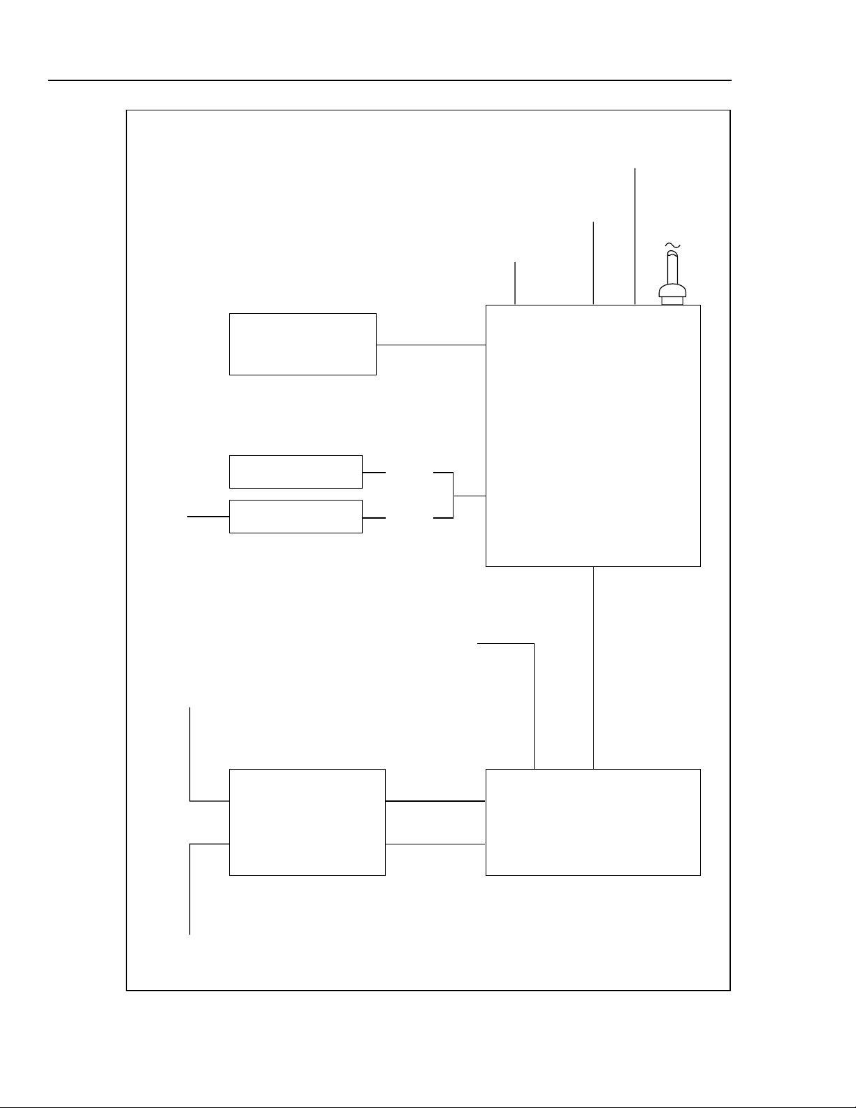
HYDRA
Service Manual
DIGITAL I/O AND
TOTALIZE INPUT
ALARM OUTPUTS
SCAN TRIGGER INPUT
AC IN
RS-232
J3J5J6J4
REAR
PANEL
CHANNELS 11…20
DISPLAY
MEMORY
IEEE
P1
P1
J1
J2
MAIN
2625A
ONLY
J1
2620A
ONLY
P10
CHANNEL 0
2-4
CHANNELS 1…10
TB1
TB2
ANALOG
INPUT
CONNECTOR
Figure 2-1. Interconnect Diagram
P1
P2 J2
J1
J10
A/D
CONVERTER
S1F.EPS
Page 53

ANALOG INPUT CONNECTOR
INPUT MULTIPLEXING
INPUT PROTECTION
INPUT SIGNAL
CONDITIONING
ANALOG
MEASUREMENT
PROCESSOR
(A/D CONVERTER)
Theory of Operation (2620A/2625A)
Functional Block Description
2
INGUARD
OUTGUARD
VACUUM FLUORESCENT
DISPLAY
DISPLAY CONTROLLER
FRONT PANEL
SWITCHES
DISPLAY ASSEMBLY
MICRO CONTROLLER
SERIAL
COMMUNICATION
µ
P
EEPROM
CALIBRATION
CONSTANTS
POWER
SUPPLY
RAM ROM
CALENDAR
CLOCK
DIGITAL KERNEL
+5.6 Vdc (Vddr)
–5.4 Vdc (Vss)
+5.3Vdc (Vdd)
A/D CONVERTER
PCA
GUARD
CROSSING
DIGITAL
I/O
RS-232
IEEE-488
OPTION -05
(2620A ONLY)
MEMORY
(2625A ONLY)
INGUARD
MAIN PCA ASSEMBLY
Figure 2-2. Overall Functional Block Diagram
–30 Vdc
+5.1 Vdc (Vcc)
–5 Vdc
5.4 Vac
OUTGUARD
s2f.eps
2-5
Page 54

HYDRA
Service Manual
2-6. Serial Com m unicat ion ( G uard Crossing)
2-7. Digital Inputs and Outputs
2-8. A/D Converter PCA
2-9. Analog Measur ement Processor
This functional block provides a high isolation voltage communication path between the
Digital Kernel of the Main PCA and the microcontroller on the A/D Converter PCA.
This bidirectional communication circuit requires power supply voltages from the Power
Supply block.
This functional block contains the Totalizer, Totalizer Debouncer, eight bidirectional
Digital I/O channels, four Alarm Outputs, and the Input Threshold control circuits. These
circuits require power supply voltages from the Power Supply, a reset signal from the
Display PCA, and signals from the Digital Kernel.
The following paragraphs describe the major blocks of circuitry on the A/D Converter
PCA.
The Analog Measurement Processor (A3U8) provides input signal conditioning, ranging,
a/d conversion, and frequency measurement. This custom chip is controlled by the A/D
Microcontroller (A3U9). The A/D Microcontroller communicates with the Main PCA
processor (A1U4) over a custom serial interface.
2-10. Input Protection Circuitry
This circuitry protects the instrument measurement circuits during overvoltage
conditions.
2-11. Input Signal Conditioning
Here, each input is conditioned and/or scaled to a dc voltage for measurement by the a/d
converter. DC voltage levels greater than 3V are attenuated. To measure resistance, a dc
voltage is applied across a series connection of the input resistance and a reference
resistance to develop dc voltages that can be ratioed. DC volts and ohms measurements
are filtered by a passive filter. AC voltages are first scaled by an ac buffer, converted to a
representative dc voltage by an rms converter, and then filtered by an active filter.
2-12. Analog-to-Digital (A/D) Convert er
The dc voltage output from the signal conditioning circuits is applied to a
buffer/integrator which charges a capacitor for an exact amount of time. The time
required to discharge this capacitor, which is proportional to the level of the unknown
input signal, is then measured by the digital counter circuits in the Analog Measurement
Processor.
2-13. Inguard Microcontroller Circuitry
This microcontroller (and associated circuitry) controls all functions on the A/D
Converter PCA and communicates with the digital kernel on the Main PCA. Upon
request by the Main PCA, the inguard microcontroller selects the input channel to be
measured through the channel selection circuitry, sets up the input signal conditioning,
commands the Analog Measurement Processor to begin a conversion, stops the
measurement, and then fetches the measurement result. The inguard microcontroller
manipulates the result mathematically and transmits the reading to the digital kernel.
2-6
Page 55

2-14. Channel Selection Circuitry
This circuitry consists of a set of relays and relay-control drivers. The relays form a tree
that routes the input channels to the measurement circuitry. Two of the relays are also
used to switch between 2-wire and 4-wire operation.
2-15. Open Thermocouple Check Circuitry
Under control of the Inguard Microcontroller, the open thermocouple check circuit
applies a small ac signal to a thermocouple input before each measurement. If an
excessive resistance is encountered, an open thermocouple input condition is reported.
2-16. Input Connector Assembly
The following paragraphs briefly describe the major sections of the Input Connector
PCA, which is used for connecting most of the analog inputs to the instrument.
2-17. 20 Channel Terminals
Twenty HI and LO terminal blocks are provided in two rows, one for channels 1 through
10 and one for channels 11 through 20. The terminals can accommodate a wide range of
wire sizes. The two rows of terminal blocks are maintained very close to the same
temperature for accurate thermocouple measurements.
Theory of Operation (2620A/2625A)
Detailed Circuit Description
2
2-18. Reference Junction Temperature
A semiconductor junction is used to sense the temperature of the thermocouple input
terminals. The resulting dc output voltage is proportional to the block temperature and is
sent to the A/D Converter PCA for measurement.
2-19. Display PCA
The Display Assembly controller communicates with the main Microprocessor over a
three-wire communication channel. Commands from the Microprocessor inform the
Display Controller how to modify its internal display memory. The Display Controller
then drives the grid and anode signals to illuminate the required segments on the
Display. The A2 Display Assembly requires power supply voltages from the Power
Supply and a clock signal from the A1U4 Microprocessor.
2-20. Memory PCA (2625A Only)
The Memory PCA is used by the Digital Kernel to store nonvolatile measurement data.
This block requires power supply voltages from the Power Supply, a reset signal from
the Display PCA, and signals from the Digital Kernel.
2-21. IEEE-488 Option (-05)
Theory of operation for the IEEE-488 Option (-05) is presented in Section 7 of this
manual. The related schematic diagram is found in Section 8.
2-22. Detailed Circuit Description
2-23. Main PCA
The following paragraphs describe the operation of the circuits on the Main PCA. The
schematic for this pca is located in Section 8.
2-7
Page 56

HYDRA
Service Manual
2-24. Power Supply Circuit Description
2-25. Raw DC Supply
The Hydra power supply consists of three major sections:
• Raw DC Supply
The raw dc supply converts line voltage (90V to 264V ac) to a dcoutput of 7.5V to
35V.
• 5V Switcher Supply
The 5V switching supply regulates the 7.5 to 35V dc input to anominal 5.1V ±0.25V
dc (VCC).
• Inverter
Using the 5V switching supply output, the inverter generates the -30Vdc, -5V dc,
and 5.4V ac supply levels needed for thevacuum-fluorescent display and the RS-232
Interface. The inverteralso provides isolated +5.3V (VDD), +5.6V (VDDR), and -
5.4V (VSS)outputs for the inguard circuitry.
The raw dc supply circuitry receives input from power transformer T401, which operates
on an input ranging from 90V to 264V ac. The power transformer is energized whenever
the power cord is plugged into the ac line; there is no on/off switch on the primary side
of the transformer. The transformer has an internal 275V ac metal-oxide varistor (MOV)
to clamp line transients. The MOV normally acts as an open circuit. When the peak
voltage exceeds approximately 400V, the line impedance in series with the line fuse
limits transients to approximately 450V. All line voltages use a slow blow 0.125 A,
250V fuse.
On the secondary side of the transformer, rectifiers A1CR2, A1CR3, and capacitor A1C7
rectify and filter the output. When it is ON, switch A1S1 (the front panel POWER
switch) connects the output of the rectifiers to the filter capacitor and the rest of the
instrument. Depending on line voltage, the output of the rectifiers is between 7.5 and
35V dc. Capacitor A1C2 helps to meet electromagnetic interference (EMI) and
electromagnetic compatibility (EMC) requirements.
When external dc power is used, the power switch connects the external dc source to
power the instrument. The external dc input uses thermistor A1RT1 (for overcurrent
protection) and diode A1CR1 (for reverse input voltage protection.) Capacitor A1C59
helps meet EMI/EMC requirements. Resistor A1R48, capacitors A1C2 and A1C39 also
ensure that the instrument meets EMI/EMC performance requirements.
2-26. Auxiliary 6V Supply
Three-terminal regulator A1U19, voltage-setting resistors A1R44 and A1R46, and
capacitor A1C34 make up the auxiliary 6-volt supply. This supply is used for the inverter
oscillator, inverter driver, and the power fail detection circuits.
2-27. 5V Switcher
The 5V switcher supply uses a switcher supply controller/switch device A1U9 and
related circuitry.The 7.5V dc to35V dc input is regulated to 5.1V dc (VCC) through
pulse-width modulation at a nominal switching frequency of 100 kHz.
The output voltage of the switcher supply is controlled by varying the duty cycle (ON
time) of the switching transistor in the controller/switch device A1U9. A1U9 contains
the supply reference, oscillator, switch transistor, pulse-width modulator comparator,
switch drive circuit, current-limit comparator, current-limit reference, and thermal limit.
2-8
Page 57

Dual inductor A1T2 regulates the current that flows from the raw supply to the load as
the switching transistor in A1U9 is turned on and off. Complementary switch A1CR10
conducts when the switching transistor is off.
The pulse-width modulator comparator in A1U9 compares the output to the reference
and sets the ON-time/OFF-time ratio to regulate the output to 5.1V dc. A1C26 is the
input filter capacitor, and A1C14 is the output filter capacitor. Proper inductor and
capacitor values set the filter frequency response to ensure best overall system stability.
Circuitry consisting of A1R26, A1C21, and A1C18 ensure that the switcher supply
remains stable and operating in the continuous mode. Resistors A1R30 and A1R31 set
the output voltage to within 5% of 5.1V.Capacitor A1C21 sets the operating frequency
of the switcher at approximately 100 kHz.
Resistors A1R30 and A1R31 form a voltage divider that operates in conjunction with
amplifier A1U31, which is configured as a voltage follower.A1U31-5 samples the 5.1V
dc output, while A1U31-6 is the voltage divider input.The effect is to maintain the
junction of R30 and R31 at 5.1V dc, resulting in an A1U31-7 output level of 6.34V dc,
or 1.24V dc above the output.This feedback voltage is applied to A1U9-2, which A1U9
interprets as 1.24V dc because A1U9-3 (ground) is connected to the 5.1V dc output.
2-28. Inverter
The inverter supply uses a two transistor driven push-pull configuration. The center tap
of transformer A1T1 primary is connected to the 5.1V dc VCC supply, and each side is
alternately connected to common through transistors A1Q7 and A1Q8. A1R38 may be
removed to disable the inverter supply for troubleshooting purposes. A1Q7 and A1Q8
are driven by the outputs of D flip-flop A1U22. Resistors A1R34 and A1R28, and diodes
A1CR11 and A1CR12 shape the input drive signals to properly drive the gate of the
transistors. D flip-flop A1U22 is wired as a divide-by-two counter driven by a 110-kHz
square wave. The 110-kHz square wave is generated by hex inverter A1U23, which is
connected as an oscillator with a frequency determined by the values of resistors A1R40
and A1R47 and capacitor A1C35. The resulting ac voltage produced across the
secondary of A1T1 is rectified to provide the input to the inverter inguard and outguard
supplies.
Theory of Operation (2620A/2625A)
Detailed Circuit Description
2
2-29. Inverter Outguard Supply
The inverter outguard supply provides three outputs: 5.4V ac, -30V dc, and -5V dc.
These voltages are required by the display and RS-232 drivers and receiver. The 5.4V ac
supply comes off the secondary windings (pins 6 and 7) on transformer T1, and it is
biased at -24V dc with zener diode A1VR3 and resistor A1R22. Dual diodes A1CR8 and
A1CR9 and capacitor A1C17 are for the -30V dc supply. Capacitors A1C30 and A1C31,
and dual diodes A1CR13 form a voltage doubler circuit that generates -12 volts. Threeterminal regulator A1U18 then regulates this voltage down to -5V for the RS-232 circuit.
Capacitor A1C32 is needed for transient response performance of the three-terminal
regulator.
2-30. Inverter Inguard Supply
The inverter inguard supply provides three outputs: +5.3V dc (VDD) and -5.4V dc
(VSS) for the inguard analog and digital circuitry, and +5.6V dc (VDDR) for the relays.
Diodes A1CR5 and A1CR6, and capacitor A1C12 are for the +9.5 volt source, and
diodes A1CR7 and capacitor A1C13 are for the -9.5V source.
Three-terminal regulator A1U6 regulates the 9.5V source to 5.6V for the relays. A1R5
and A1R6 set the output voltage at 5.6V. A1C6 is required for transient performance.
The +5.3V regulator circuit uses A1Q2 for the series-pass element and A1Q4 as the error
2-9
Page 58

HYDRA
Service Manual
2-31. Power Fail Detection
amplifier. A1VR2 is the reference for the positive supply. A1R14 provides the current to
bias the reference zener. A1C4 is the output filter, and A1C9 provides frequency
compensation of the regulator circuit. Transistor A1Q1 and resistor A1R13 make up the
current-limit circuit.
When the voltage across A1R13 increases enough to turn on A1Q1, output current is
limited by removing the base drive to A1Q2.
The -5.4 volt regulator operates like the +5.3 volt regulator, except that the NPN
transistors in the positive supply are PNP transistors in the negative supply, and the PNP
transistors in the positive supply are NPN transistors in the negative supply. If a VDDto-VSS short circuit occurs, diode A1CR4 ensures that current limit occurs at the limit
set for the -5.4V dc or +5.3V dc supply, whichever is lower.
The power fail detection circuit generates a signal to warn the Microprocessor that the
power supply is going down. Comparator A1U24 compares the divided-down raw
supply voltage and the band-gap generated reference voltage. When the raw supply
voltage is greater than about 8V dc, the output of A1U24 is "high" and when the raw
supply falls below 8V dc, the output goes "low". Resistors A1R39 and A1R41 make up
the divider, and resistor A1R43 provides bias for the band-gap reference. Resistor
A1R42 is a pull up resistor for the comparator output, and resistor A1R45 provides
positive feedback to provide the comparator with some hysteresis.
2-32. Digital Kernel
The Digital Kernel is composed of the following eight functional circuit blocks: the
Microprocessor, the ROM (Read-Only Memory), the NVRAM/Clock (Nonvolatile
Random Access Memory and Real-Time Clock), the EEPROM (Electrically Erasable
Programmable Read-Only Memory), the Counter/Timer, the RS-232 Interface, and the
Option Interface.
2-33. Microprocessor
The Microprocessor uses an eight-bit data bus and a sixteen-bit address bus to access
memory locations in the ROM (A1U8), the NVRAM/Clock (A1U3), the Counter/Timer
(A1U2), the Digital I/O Registers (A1U13, A1U16, A1U26), the Memory PCA (A6),
and the IEEE-488 PCA (A5).
The Microprocessor oscillator operates at a 4.9152-MHz frequency determined by
crystal A1Y1. The A1U4-68 system clock signal (the Microprocessor oscillator
frequency divided by four) is a square wave with a frequency of 1.2288 MHz. This
system clock also determines the memory cycle time of 0.813 microseconds. The system
clock is also used by the Display Assembly and the IEEE-488 option assembly after
being damped by series resistor A1R19 to minimize the EMI generated by this signal’s
sharp edges.
When the address bus is stable, the Microprocessor enables either the reading of memory
(by driving RD*, A1U4-67, low) or writing of memory (by driving WR*, A1U4-66,
low.)
2-10
The Microprocessor uses a three-wire synchronous communication interface to store and
retrieve instrument communication configuration and calibration information in the
EEPROM (A1U1). See the EEPROM description for more detailed information.
The Microprocessor communicates to the Display Controller using another synchronous,
three-wire communication interface described in detail in the Display Controller Theory
of Operation in this section.
Page 59

The Microprocessor communicates to the Microcontroller on the A/D Converter PCA
(via the Serial Communication circuit) using an asynchronous communication protocol
at 4800 baud. Communication to the Microcontroller (A3U9) originates at A1U4-11.
Communication from the A/D’s Microcontroller to the Microprocessor appears at A1U4-
10. When there is no communication in progress between the Microprocessor and the
Microcontroller, both of these signals are low.
2-34. Address Decoding
The upper three bits of the address bus are decoded by A1U10-3,4,5 to generate the
ROM* chip select signal for the ROM (A1U10-6).
The NVRAM/Clock chip select signal (A1U21-6 going low) is generated when the
ROM* and RESET* signals are high and any one of address bits 9 through 12 is high.
To avoid spurious write cycles during power cycling, the INT* output of the NVRAM
(A1U3-1) is used to discharge the reset circuit on the Display PCA through resistor
A1R63 when the power supply level at A1U3-28 is too low (less than approximately
4.65V dc) to allow memory operations to the NVRAM.
The miscellaneous I/O chip select (hexadecimal addresses 0000 through 01FF) is
decoded using the ROM* signal and address bits 9 through 12 by A1U15 and A1U21.
When ROM* is high and all four of the address bits are low, the I/O* signal (A1U21-8)
is low. The I/O* signal and address bits 3 through 8 are then used by A1U10 and A1U11
to generate the CNTR*, DIO*, IEEE*, and MEM* chip select signals.
Theory of Operation (2620A/2625A)
Detailed Circuit Description
2
Table 2-1 shows a memory map for the Microprocessor.
Table 2-1. Microprocessor Memory Map
Hexadecimal Address Device Selected
2000 - FFFF ROM (A1U8)
1FF8 - 1FFF Real-Time Clock (A1U3)
0200 - 1FF7 NVRAM (A1U3)
0040 - 013F Microprocessor Internal RAM
0038 - 003F Counter/Timer (A1U2)
0032 (Read Only) Digital Inputs (A1U13)
0032 (Write Only) Digital Outputs (A1U26)
0035 (Write Only) Alarm Outputs (A1U16)
0028 - 002F IEEE-488 Option (2620A Only)
0005 - 0006 (Write Only) Memory Page (2625A Only)
0004 Memory Data (2625A Only)
2-35. Serial Communication (Guard Crossing)
The transmission of information from the Microprocessor (A1U4) to the Microcontroller
(A3U9) is accomplished via the circuit made up of A1U15, A1U7, A1R8, A1R16, and
A3R8. The transmit output from the Microprocessor (A1U4-11) is inverted by A1U15,
which drives the optocoupler LED (A1U7-2). Resistor A1R8 limits the current through
the LED.
The phototransistor in A1U7 responds to the light emitted by the LED when A1U7-2 is
driven low (the collector of the phototransistor (A1U7-5) goes low.) The phototransistor
collector is pulled up by A3R8 on the A/D Converter PCA. When turning off, the
2-11
Page 60

HYDRA
Service Manual
2-36. Display/Keyboard Interface
phototransistor base discharges through A1R16. With this arrangement, the rise and fall
times of the phototransistor collector signal are nearly symmetrical.
The transmission of data from the Microcontroller (A3U9) to the Microprocessor
(A1U4) is accomplished via the circuit made up of A3Q1, A3R7, A1U5, A1R7, and
A1R3. The transmit output from the Microcontroller (A3U9-14) is inverted by A3Q1,
which drives the optocoupler LED (A1U5-2) through resistor A3R7. The current through
the LED is limited by resistor A3R7. The phototransistor in A1U5 responds to the light
emitted by the LED when A1U5-2 is driven low; the emitter of the phototransistor
(A1U5-4) goes high. The phototransistor collector (A1U5-5) is pulled up by VCC, and
the emitter is pulled down by resistor A1R3. When turning off, the phototransistor base
discharges through A1R7. With this arrangement, the rise and fall times of the
phototransistor collector signal are nearly symmetrical.
The Microcontroller sends information to the Display Processor via a three-wire
synchronous communication interface. The detailed description of the DISTX, DISRX,
and DSCLK signals may be found in the detailed description of the Display PCA. Note
that the DISRX signal is pulled down by resistor A1R1 so that Microprocessor input
A1U4-15 is not floating at any time. The Display PCA also provides the system reset
circuitry and watchdog timer.
The Keyboard interface is made up of six bidirectional port lines from the
Microcontroller. SWR1 through SWR6 (A1U4-21 through A1U4-26, respectively) are
pulled up by A2Z1 on the Display PCA. The detailed description of the Display PCA
describes how the Microprocessor interfaces to the Keyboard.
2-37. ROM
The ROM provides the instruction storage for the Microprocessor. The chip select for
this device (A1U8-20) goes low for any memory cycle between hexadecimal addresses
2000 and FFFF (accessing 56 kbytes). Whenever this device is chip selected for read, the
instruction in the addressed location is output to the data bus and read by the
Microprocessor.
2-38. NVRAM/Clock
The NVRAM/Clock (A1U3) provides the data storage and real-time clock for the
instrument. A lithium battery, a crystal, and an automatic power-fail control circuit are
also integrated into this single package. When the RAM* chip select signal (A1U3-20) is
low, the Microprocessor is accessing one of the 8192 bytes in the NVRAM/Clock. The
RD* (A1U3-22) and WR* (A1U3-27) signals go low to indicate a read or write cycle,
respectively.
The internal power-fail control circuit disables access to this device and drives the INT*
output (A1U3-1) low when the VCC power supply is below approximately +4.5V dc.
This action keeps locations in the NVRAM/Clock from being modified while the
instrument is powering up and down. When the INT* output is low, the reset circuit on
the Display PCA is discharged, and a system reset occurs. Therefore, the Microprocessor
is reset on power failure as soon as it can no longer access the NVRAM/Clock.
2-12
The NVRAM contains 8184 bytes of nonvolatile data storage. The nonvolatile
instrument configuration information, the nonvolatile measurement data, and the
Microprocessor temporary data are stored in this area.
The Clock is composed of 8-byte wide registers that allow access to the real-time clock
counters. The Microprocessor accesses these registers in the same way as the NVRAM.
Page 61

2-39. EEPROM
The EEPROM contains 64 registers, each of which is 16 bits long. These registers are
used to provide nonvolatile storage of some of the instrument configuration information
and all of the calibration information. When the Microprocessor is communicating to the
EEPROM, Chip Select input (A1U1-1) is driven high to enable the EEPROM interface.
When the Microprocessor is reading data from the EEPROM, the data bits are serially
shifted out on the Data Out signal (A1U1-4) with each one-to-zero transition of the
Serial Clock (A1U1-2).
When the Microprocessor is writing commands and data to the EEPROM, the bits are
serially shifted into the EEPROM on the Data In signal (A1U1-3) with each zero-to-one
transition of the Serial Clock (A1U1-2). When the last data bit for an erase or write
operation is shifted into the EEPROM, the Microprocessor pulses the Chip Select input
(A1U1-1) low to start the operation. The EEPROM will then drive the Data Out signal
(A1U1-4) low to indicate that it is busy writing the register. The Data Out signal goes
high when the operation is complete. Since the Microprocessor waits for this signal to go
high before doing anything else, an EEPROM failing to drive this signal high causes the
Microprocessor to wait until the Watchdog Timer on the Display PCA resets the
instrument.
The Chip Select input (A1U1-1) is always set low at the end of each EEPROM
operation.
Theory of Operation (2620A/2625A)
Detailed Circuit Description
2
2-40. Counter/Timer
The Counter/Timer IC (A1U2) has three 16-bit counters that are used both to implement
the Totalizer function and to provide a periodic 50-millisecond interrupt used for interval
time operation.
The output from the Totalizer Input circuit (A1U28-3) provides the clock input for
Counter 2. Counter 2 operates as a 16-bit pre-loadable down counter for the Totalizer
function. This counter causes the IRQ1* interrupt (A1U2-9) to go low, interrupting the
Microprocessor when the counter value changes from hexadecimal 0000 to FFFF. The
Counter 2 Gate input (A1U2-2) must be low for the Totalizer to operate correctly.
Counter 3 is used as a periodic 50.0-millisecond interrupt source. This counter divides
the E clock input (A1U2-17) by 61440. The IRQ1* interrupt (A1U2-9) goes low
(interrupting the Microprocessor) at the end of each 50.0-millisecond period. The
Counter 3 Gate input (A1U2-5) and the Counter 3 Clock input (A1U2-7) should both be
low for this counter to operate correctly. The 10-Hz square wave signal observed on the
Counter 3 Output pin (A1U2-6) changes state every 50.0 milliseconds.
Counter 1 is not used in the instrument, but its Clock and Output pins have been
connected to available pins on the Option Interface.
2-41. RS-232 Interface
The RS-232 interface is composed of connector A1J4, RS-232 Driver/Receiver A1U25,
and the hardware serial communication interface (SCI) in Microprocessor A1U4.
The SCI transmit signal (A1U4-14) goes to the RS-232 driver (A1U25-12), where it is
inverted and level shifted so that the RS-232 transmit signal transitions between
approximately +5.0 and -5.0V dc. When the instrument is not transmitting, the driver
output A1U25-5 is approximately -5.0V dc. The RS-232 receive signal from A1J4 goes
to the RS-232 receiver A1U25-4, which inverts and level shifts the signal so that the
input to the SCI transitions between 0 and +5.0V dc. When nothing is being transmitted
to the instrument, the receiver output (A1U25-13) is +5.0V dc.
2-13
Page 62

HYDRA
Service Manual
2-42. Option Interface
Data Terminal Ready (DTR) is a modem control signal controlled by the
Microprocessor. When the instrument is powered up, the Microprocessor port pin
(A1U4-32) goes high, which results in the RS-232 driver output (A1U25-7) going to -
5.0V dc. When the instrument has initialized the SCI and is ready to receive and
transmit, A1U4-32 will go low, resulting in the RS-232 DTR signal (A1U25-7) going to
+5.0V dc. The RS-232 DTR signal remains at +5.0V dc until the instrument is powered
down.
The interconnection to the option slot is implemented by J1 on the Main PCA. This
connector (A1J1) routes the outguard logic power supply (VCC and GND), the eight-bit
data bus, RD*, WR*, E, RESET*, IEEE*, MEM*, and the lower three bits of the address
bus to the option installed in the option slot. This connector also routes an interrupt
signal from the IEEE-488 option to the IRQ2* input of the Microprocessor.
An option sense signal from the installed option allows the Microprocessor to identify
the type of option. When the instrument is powered up, the type of PCA installed in the
option slot is determined by the Microprocessor by driving the IRQ2* signal (A1U4-20)
and sensing the activity on the OPS* signal (A1U4-29). The Microprocessor first sets
IRQ2* low and samples the OPS* input, then sets IRQ2* high and samples the OPS*
input again. Table 2-2 describes how this information is used to determine what
hardware is installed in the option slot.
IRQ2* Output
0100
1101
2-43. Digital I/O
The following paragraphs describe the Digital Input Threshold, Digital Input Buffers,
Digital and Alarm Output Drivers, Totalizer Input, and External Trigger Input circuits.
Table 2-2. Option Type Sensing
State of *OPS Input for PCA:
None Installed IEEE-488 Memory
2-14
Page 63

Theory of Operation (2620A/2625A)
Detailed Circuit Description
2-44. Digital Input Threshold 2-1.
The Digital Input Threshold circuit sets the input threshold level for the Digital Input
Buffers and the Totalizer Input. A software programmable voltage divider (A1U17,
A1R35, A1R36, A1R37) and a unity gain buffer amplifier (A1AR1) are the main
components in this circuit. The Microprocessor sets outputs A1U16-15 and A1U16-12 to
select one of four input threshold levels. These outputs control the resistive divider
(A1R35, A1R36, A1R37) via two drivers with open-collector outputs in A1U17. The
voltage from the divider is then buffered by A1AR1 which sets the input threshold.
Capacitor A1C29 filters the divider voltage at the input of A1AR1. Table 2-3 defines the
programmable input threshold levels.
The instrument selects the +1.4V dc threshold level at power-up initialization.
Table 2-3. Programmable Input Threshold Levels
A1U16-15 A1U16-12 Input Threshold Voltage
00+2.5V dc
01+0.7V dc
10+1.4V dc
11+0.7V dc
2
2-45. Digital Input Buffers
Since the eight Digital Input Buffers are identical in design, only components used for
Digital Input 0 are referenced in this description. If the Digital Output Driver (A1U27-
16) is off, the input to the Digital Input Buffer is determined by the voltage level at
A1J5-10. If the Digital Output Driver is on, the input of the Digital Input Buffer is the
voltage at the output of the Digital Output Driver.
The Digital Input Threshold circuit and resistor network A1Z1 determine the input
threshold voltage and hysteresis for inverting comparator A1AR2. The inverting input of
the comparator (A1AR2-2) is protected by a series resistor (A1Z3) and diode A1CR14.
A negative input clamp circuit (A1Q9, A1Z2, and A1CR17) sets a clamp voltage of
approximately +0.7V dc for the protection diodes of all Digital Input Buffers. A negative
input voltage at A1J5-10 causes A1CR14 to conduct current, clamping the comparator
input A1AR2-2 at approximately 0V dc.
The input threshold of +1.4V dc and a hysteresis of +0.5V dc are used for all Digital
Input Buffers. When the input of the Digital Input Buffer is greater than approximately
+1.65V dc, the output of the inverting comparator is low. When the input then drops
below about +1.15V dc, the output of the inverting comparator goes high.
2-46. Digital and Alarm Output Drivers
Since the 12 Digital Output and Alarm Output Drivers are identical in design, the
following example description references only the components that are used for Alarm
Output Driver 0.
The Microprocessor controls the state of Alarm Output Driver 0 by writing to latch
output A1U16-2. When A1U16-2 is set high, the output of the open-collector Darlington
driver (A1U17-15) sinks current through current limiting resistor A1R62. When A1U162 is set low, the driver output turns off and is pulled up by A1Z2 and/or the voltage of
the external device that the output is driving. If the driver output is driving an external
inductive load, the internal flyback diode (A1U17-9) conducts the energy into MOV
A1RV1 to keep the driver output from being damaged by excessive voltage. Capacitor
A1C58 ensures that the instrument meets electromagnetic interference (EMI) and
electromagnetic compatibility (EMC) performance requirements.
2-15
Page 64

HYDRA
Service Manual
2-47. Totalizer Input
The Totalizer Input circuit consists of Input Protection, a Digital Input Buffer circuit,
and a Totalizer Debouncer circuit. The Digital Input Buffer for the totalizer is protected
from electrostatic discharge (ESD) damage by A1R49 and A1C43. Refer to the detailed
description of the Digital Input Buffer circuit for more information.
The Totalizer Debounce circuit allows the Microprocessor to select totalizing of either
the input signal or the debounced input signal. Latch output A1U16-16 is set low by
A1U4 to totalize the unmodified input signal or high to totalize the debounced input
signal. This totalizer clock control is provided by A1U28; output A1U28-3 drives the
totalizer counter clock input (A1U2-4).
The actual debouncing of the input signal is accomplished by A1U14, A1U20, and
A1U29. An EXOR gate compares the input signal (A1U14-13) and the output of an
eight-bit shift register (A1U29-9). If these signals differ, EXOR gate output A1U14-11
goes high, enabling counter A1U20 and shift register A1U29. The counter divides the
system clock of 1.2288 MHz (A1U20-10) by 256 to yield a 4.8-kHz clock (A1U20-13).
This signal clocks the eight-bit shift register. After approximately 1.5625 milliseconds,
the input signal will have been shifted from the serial input (A1U29-10) through to the
eighth output bit (A1U29-9). This forces the counter and shift register to stop. If the
input signal changes state before 1.5625 milliseconds have elapsed, the counter is
cleared and the shift register is preloaded again. Therefore, the input signal must remain
stable for greater than 1.5625 milliseconds before that transition changes the state of the
clock input of the totalizer counter (A1U2-4).
2-48. External Trigger Input Circuits
The External Trigger Input circuit can be configured by the Microprocessor to interrupt
on a rising or falling edge of the XT* input (A1J6-2) or to not interrupt on any
transitions of the XT* input.
The Microprocessor sets latch output A1U16-19 high for falling edge detection and low
for rising edge detection of the XT* input. The Microprocessor can enable the external
trigger interrupt by setting port pin A1U4-28 high or disable the interrupt by setting it
low. Microprocessor port pin A1U4-28 should only be high if the instrument trigger
mode of "ON" has been selected. Resistor A1R20 pulls NAND gate input A1U13 low
during power-up to ensure that the external trigger interrupt input (A1U4-9) is high.
When the EXOR gate output (A1U14-3) goes high, and NAND gate input A1U12-13 is
high, the output of the NAND gate (A1U12-11) goes low to interrupt the
Microprocessor. The Microprocessor can also determine the state of the XT* input by
reading the TRIG signal on port pin A1U4-27.
The XT* input is pulled up to +5V dc by A1Z2 and is protected from damage by ESD by
A1R58, A1C54, A1Z3, and A1CR15. Capacitor A1C54 helps ensure that the instrument
meets EMI/EMC performance requirements.
2-49. A/D Converter PCA
The following paragraphs describe the operation of the circuits on the A/D Converter
PCA. The schematic for this pca is located in Section 8.
2-16
2-50. Analog Measurement Processor
Refer to Figure 2-3 for an overall picture of the Analog Measurement Processor chip and
its peripheral circuits. Table 2-4 describes Analog Measurement Processor chip signal
names.
Page 65

Theory of Operation (2620A/2625A)
Detailed Circuit Description
The Analog Measurement Processor (A3U8) is a 68-pin CMOS device that, under
control of the A/D Microcontroller (A3U9), performs the following functions:
• Input signal routing
• Input signal conditioning
• Range switching
• Passive filtering of dc voltage and resistance measurements
• Active filtering of ac voltage measurements
• A/D conversion
• Support for direct volts, true rms ac volts, temperature, resistance,and frequency
measurements
Two separate signal paths are used, one for dc/ohms/temperature and one for ac. The
volts dc (3V range and below) and temperature voltages are coupled directly to the a/d
converter, while higher voltages are attenuated first. For ohms, the dc circuitry is
augmented with an internal ohms source voltage regulator controlled through an extra set
of switches. For volts ac, inputs are routed through the ac buffer, which uses the gain
selected by the Measurement Processor (A3U8).
The a/d converter uses a modified dual-slope minor cycle method. The basic
measurement unit, a minor cycle, consists of a fixed time integrate period for the
unknown input, a variable time reference integrate period, a variable time hold period,
and various short transition periods. A minor cycle period lasts for 25 ms or until a new
minor cycle is begun, whichever comes first.
2
2-51. Input Protection
The instrument measurement circuits are protected when overvoltages are applied
through the following comprehensive means:
• Any voltage transients on channel 0 HI or LO terminals areimmediately clamped to
a peak of about 1800V or less by MOVs A3RV1and A3RV2. (This is much lower
than the 2500V peaks that can beexpected on 240 VAC, IEC 664 Installation
Category II, ac mains.)
• Fusible resistors A3R10 and A3R11 protect the measurement circuitryin all
measurement modes by limiting currents.
• A3Q11 clamps voltages exceeding 0.7V below and approximately 6.0Vabove analog
common (LO) or LO SENSE, with A3R35 limiting the inputcurrent.
• A3Q10 clamps voltages during ohms measurements with A3RT1, A3R34,A3R10,
and A3Z4 limiting the input current. With large overloads,thermistor A3RT1 will
heat up and increase in resistance.
• A3U8 also clamps voltages on its measurement input pins that exceedthe VDD and
VSS supply rails. Resistors A3R42, A3R11, A3R10, A3RT1,A3Z4, A3R35, and
A3R34 limit any input currents.
• Any excessive voltages that are clamped through A3U8 to VDD or VSS,are then
also clamped by zener diodes A3VR3 and A3VR2.
• The open thermocouple detect circuitry is protected against voltagetransient damage
by A3Q14 and A3Q15.
• When measuring ac volts, the ac buffer is protected by dual-diodeclamp A3CR1 and
resistor network A3Z3.
• Switching induced transients are also clamped by dual-diodeA3CR4 and capacitor
A3C33, and limited by resistor A3R33.
2-17
Page 66
HYDRA
Service Manual
ACV
ACTIVE
FILTER
RMS
CONVERTER
61
25678
S81
COUNTER
FREQUENCY
S42
ACTIVE
FILTER
S19
60
+
AMP
A/D LO
S18
VR1
VDD
A/D
C12
1.05V
A/D
RRS LOW
REF
52
DIGITAL
SECTION
U8 ANALOG
PROCESSOR*
MEASUREMENT
3.84 MHz
DC
FILTERS
PASSIVE
59
585756
–
RRS
LOW
A/D HI
DC HI
Z2
51
RRS HI
C31
ACV
GAIN CONTROL
AC BUFFER
K15
S16
10
R32
LOW
11
Ω LO
R35
DIVIDER
SWITCHING
13
14
Ω
300
1K
V LO/RRS LO
R34
10K
Ω
R10
15
300V
K16
Ω
3 K
1M
TO
REFERENCE
RESISTOR
OHMS
SOURCE
S3
RRS HI
TO OHMS
SOURCE &
16
19
21
S2
23
VOLTAGE
28 29 30 31 32 33 36 37 39 40 41 42
25
TO U9 TO U9
* NOT ALL U8 SWITCHES ARE SHOWN HERE.
REFER TO THE SCHEMATIC DIAGRAM IN SECTION 8.
Ω
30V
30 K
300 KΩ
3 MΩ, 10 MΩ
100K
30 VDC
10M
300 VDC
Z4
R42
K17
OPEN
DETECT
THERMOCOUPLE
TO U9
Ω
3 VDC/300 MVDC/TC/
RRS = REFERENCE RESISTOR SENSE
R11
R43
2-18
JUNCTION
REFERENCE
HI
SOURCE
HI
LO
SENSE
LO
SENSE
SOURCE
Figure 2-3. Analog Simplified Schematic Diagram
s3f.eps
Page 67

Table 2-4. Analog Measurement Processor Pin Descriptions
Pin Name Description
Theory of Operation (2620A/2625A)
Detailed Circuit Description
2
1
2
3
4
5
6
7
8
9
10
11
12
13
14
15
16
17
18
19
20
21
22
23
24
25
VDD
ACBO
AIN
AGND2
ACR4
ACR3
ACR2
ACR1
VSSA
REFJ
DCV
LOW
GRD
RRS
V4
V3
V1
GRD
V2F
V2
GRD
V0
GRD
OVS
GRD
AGND1
+5.4V supply
AC buffer output
(not used)
Analog ground
AC buffer range 4 (300V)
AC buffer range 3 (30V)
AC buffer range 2 (3V)
AC buffer range 1 (300 mV)
-5.4V supply for AC ranging
Reference junction input
A/D converter low input
Driven guard
Reference resistor sense for ohms
Tap #4 on the DCV input divider/ohms reference network
Tap #3 on the DCV input divider/ohms reference network
Tap #1 on the DCV input divider/ohms reference network
Driven guard
Tap #2 input on the DCV input divider/ohms reference network
Tap #2 on the DCV input divider/ohms reference network
Driven guard
Tap #0 on the DCV input divider/ohms reference network
Driven guard
Ohms and volts sense input
Guard
Analog ground
26
27
28
29
30
31
32
33
34
35
36
37
38
39
40
41
42
43
44
45
DGND
FC0
FC1
FC2
FC3
FC4
FC5
FC6
FC7
XIN
XOUT
MRST
AS
AR
SK
CS
BRS
VSS
INT
(not used)
Analog ground
Function control #0
Function control #1
Function control #2
Function control #3
(not used)
(not used)
Function control #6
Function control #7
Crystal oscillator input
Crystal oscillator output
Master reset
Analog send
Analog receive
Serial clock
Chip select
(not used)
-5.4V dc
Integrator output
2-19
Page 68

HYDRA
Service Manual
Table 2-4. Analog Measurement Processor Pin Descriptions (cont)
Pin Name Description
46
47
48
49
50
51
52
53
54
55
56
57
58
59
60
61
62
63
64
65
66
67
68
SUM
B.1
B.32
B1
B3.2
VREF+
VREFRAO
RA+
RA-
AFO
MOF
AFI
FAI
FAO
RMSF
AGND3
RMSG
2
RMSO
CAVG
VSSR
RMSG
1
RMSI
Integrator summing node
Buffer output, 100 mV range
Buffer output, 300 mV range
Buffer output, 1000 mV range
Buffer output, 3V range
A/D voltage reference plus
A/D voltage reference minus
A/D reference amplifier output
A/D reference amplifier noninverting input
A/D reference amplifier inverting input
Passive filter 2
Passive filter 1 plus resistance
Passive filter 1
Filter amplifier inverting input
Filter amplifier output
RMS output, filtered
(not used, connected to filtered -5.4V dc)
(not used)
RMS converter output
(not used)
-5.4V dc, filtered
(not used, pulled to filtered -5.4V dc)
(not used)
2-20
2-52. Input Signal Conditioning
Each input is conditioned and/or scaled to a dc voltage appropriate for measurement by
the a/d converter. DC voltage applied to the a/d converter can be handled on internal
ranges of 0.1V, 0.3V, 1V, or 3V. Therefore, high-voltage dc inputs are scaled, and ohms
inputs are converted to a dc voltage. Line voltage level ac inputs are first scaled and then
converted to a dc voltage. Noise rejection is provided by passive and active filters.
2-53. Function Relays
Latching relays A3K15, A3K16, and A3K17 route the input signal to the proper circuit
blocks to implement the desired measurement function. These relays are switched when
a 6-millisecond pulse is applied to the appropriate reset or set coil by the NPN
Darlington drivers in IC A3U10. The A/D Microcontroller A3U9 controls the relay drive
pulses by setting the outputs of port 6. Since the other end of the relay coil is connected
to the VDDR supply, a magnetic field is generated, causing the relay armature and
contacts to move to (or remain in) the desired position. Function relay states are defined
in Table 2-5.
Page 69

Table 2-5. Function Relay States
Function A3K17 A3K16 A3K15
DC mV, 3V,Thermocouples Reset Set Set
DC 30V, 300V Set Set Set
ACV Set Set Reset
Ohms, RTDs Reset Reset Set
Frequency Set Set Reset
2-54. DC Volts and Thermocouples
For the 3V and lower ranges (including thermocouples), the HI input signal is applied
directly to the A3U8 analog processor through A3R11, A3K17, and A3R42. Capacitor
A3C27 filters this input, which the analog processor then routes through S2 and other
internal switches, through the passive filter, and to the internal a/d converter. The LO
SENSE signal is applied to A3U8 through A3R35 and routed through internal switch
A3U8-S19 to LO of the a/d converter.
Guard signals MGRD and RGRD are driven by an amplifier internal to A3U8 to a
voltage appropriate for preventing leakage from the input HI signal under high humidity
conditions.
For the 30V range, the HI signal is scaled by resistor network A3Z4. Here, the input is
applied to pin 1 of A3Z4 so that an approximate 100:1 divider is formed by the 10-MΩ
and 100.5-kΩ resistors in A3Z4 when analog processor switches S3 and S13 are closed.
The attenuated HI input is then sent through internal switch S12 to the passive filter and
the a/d converter. Input LO is sensed through analog processor switch S18 and resistor
A3R34.
For the 300V range (Figure 2-4), the HI signal is again scaled by A3Z4. The input is
applied to pin 1 of A3Z4, and a 1000:1 divider is formed by the 10-MΩ and 10.01-kΩ
resistors when switches S3 and S9 are closed in A3Z4. The attenuated HI input is then
sent through internal switch S10 to the passive filter and the a/d converter. LO is sensed
through analog processor switch S18 and resistor A3R34.
Relay Position
Theory of Operation (2620A/2625A)
Detailed Circuit Description
2
2-55. Ohms and RTDs
Resistance measurements are made using a ratio ohms technique, as shown in Figure 2-
5. A stable voltage source is connected in series with the reference resistor in A3Z4 and
the unknown resistor. Since the same current flows through both resistors, the unknown
resistance can be determined by multiplying the ratio of the voltage drops across the
reference and the unknown resistors by the known reference resistor value.
For the RTD, 300Ω, 3-kΩ, and 30-kΩ ranges, the ratio technique is implemented by
integrating the voltage across the unknown resistance for a fixed period of time and then
integrating the negative of the voltage across the reference resistance for a variable time
period. In this way, each minor cycle result gives the ratio directly.
For the 300-kΩ, 3-MΩ, and 10-MΩ ranges, the ratio is determined by performing two
separate voltage measurements in order to improve noise rejection. One fixed-period
integration is performed on the voltage across the unknown resistance, and the second
integration is performed on the voltage across the reference resistance. The ratio of the
two fixed-period voltge measurements is then computed by Microcontroller A3U9. The
resistance measurement result is determined when A3U9 multiplies the ratio by the
reference resistance value.
2-21
Page 70
HYDRA
Service Manual
S2
A3R11
A3K17
INPUT HI
A3R10
A3Z4
10M
S3
S9
INPUT LO
S10
A3Z4
10.01k
A3K16
Figure 2-4. DC Volts 300V Range Simplified Schematic
A3R34
PASSIVE
FILTER
HIGH
LOW
When an input is switched in for a measurement, the ohms source in Analog Processor
A3U8 is set to the correct voltage for the range selected and is connected to the
appropriate reference resistor in network A3Z4. A measurement current then flows
through A3Z4, relay A3K16, thermistor A3RT1, resistor A3R10, the unknown
resistance, A3R43, ground, and the ohms source.
The resulting voltage across the unknown resistance is integrated for a fixed period of
time by the A/D Converter through the HI SENSE path of A3R11, A3K17, A3R42 and
A3U8 switch S2, and the LO SENSE path of A3R35 and Analog Processor switch S19.
Passive filtering is provided by A3C34, A3C27, and portions or all of the DC Filter
block.
A/D
s4f.eps
2-22
The voltage across the reference resistor for the 300Ω and RTD, 3-kΩ, and 30-kΩ
ranges (the 1-kΩ, 10.01-kΩ, and 100.5-kΩ resistances in A3Z4, respectively) is
integrated for a variable period of time until the voltage across the integrate capacitor
reaches zero. For the 300Ω and RTD range, the reference resistor voltage is switched in
through Analog Processor switch S6 and applied to the A/D Converter by switch S8. For
the 3-kΩ range, switches S9 and S11 perform these functions, respectively. For the 30kΩ range, switches S13 and S14 are used. For all ranges, the voltage is routed through
A3R34 to the RRS input.
Page 71

VR
A3K16
A3RT1 & A3R10
OHMS
VOLTAGE
SOURCE
IX
+
REF
–
A3R11
HI
R
A3K17
REF
A3Z4
REFERENCE
RESISTOR
A3R42
A3R34
PASSIVE
FILTER
Theory of Operation (2620A/2625A)
Detailed Circuit Description
LOW
A/D
INTEGRATE
REFERENCE
HIGH
HIGH
2
+
R
X
X
VR
VR
X
REF
VR
LO
=
UNKNOWN
RESISTOR
X•RX
I
IX•RREF
X
R
=
R
REF
Figure 2-5. Ohms Simplified Schematic
A/D
INTEGRATE
UNKNOWN
LOW
s5f.eps
The reference resistor for the 300-kΩ, 3-MΩ, and 10-MΩ ranges is the 1-MΩ resistor in
A3Z4, which is selected by S15. The voltage across this reference is integrated during its
own minor cycle(s) and is switched to a passive filter and the A/D Converter by switches
S1 and S18.
When 4-wire measurements are made on any of the six ranges, separate Source and
Sense signal paths are maintained to the point of the unknown resistance. The 4-wire
Source path measurement current is provided by the A3U8 ohms source through one of
the A3U8 internal switches (S6, S9, S13, or S15) and the appropriate reference resistor
in A3Z4. The current flows through relay A3K16, thermistor A3RT1, resistor A3R10,
the HI Source instrument relay contacts (A3K1 - A3K3, A3K5 - A3K14), and the HI
Source lead wire, to the unknown resistance to be measured. The current flows back
through the LO Source lead wire, the LO Source path of the instrument relays (A3K1 A3K3, A3K5 - A3K14), resistor A3R43, and analog ground, to the A3U8 ohms source.
The voltage that develops across the unknown resistance is sensed through the other 2
wires of the 4-wire set. HI is sensed through the HI Sense path made up of the users HI
Sense lead wire, the HI Sense contacts in the instrument relays, resistor A3R11, relay
A3K17, resistor A3R42, and Analog Processor A3U8 switch S2. LO is sensed through
the users LO Sense lead wire, the LO Sense contacts in the instrument relays, protection
resistor A3R35, and A3U8 switch S19.
2-23
Page 72

HYDRA
Service Manual
2-56. AC Volts
Since virtually no current flows through the sense path, no error voltages are developed
that would add to the voltage across the unknown resistance; this 4-wire measurement
technique eliminates user lead-wire and instrument relay contact and circuit board trace
resistance errors.
AC-coupled ac voltage inputs are scaled by the ac buffer, converted to dc by a true rms
ac-to-dc converter, filtered, and then sent to the a/d converter.
Refer to Figure 2-6. Input HI is switched to the ac buffer by dc-blocking capacitor
A3C31, protection resistor A3R11, and latching relay A3K15. Resistor A3R44 and
A3K15 act to discharge A3C31 between channel measurements. LO is switched to the
A3U8 A/D Converter through A3R34 and S18.
INPUT HI
INPUT LO
A3R11
A3R43
A3K15
A3C31
A3R44
Figure 2-6. AC Buffer Simplified Schematic
A3Z3
1.111M
_
+
A3Z3 FEEDBACK
RESISTOR
A3U7
A3C15
&
A3C16
A3Z3
2.776k
A3Z3
115.7
JFETs A3Q3 through A3Q9 select one of the four gain (or attenuation) ranges of the
buffer (wide-bandwidth op-amp A3U7.) The four JFET drive signals ACR1 through
ACR4 turn the JFETs on at 0V and off at -VAC. Only one line at a time will be set at 0
volts to select a range.
A3U6
RMS
COVERTER
s6f.eps
2-24
The input signal to the buffer is first divided by 10, 100, or 1000 for the 300 mV, 3V,
and 30V ranges, respectively. The resistance ratios used are summarized in Table 2-6.
Note that the 111.1-kΩ resistor is left in parallel with the smaller (higher attenuation)
resistors. The attenuated signal is then amplified by A3U7, which is set for a gain of 25
by the 2.776-kΩ and 115.7Ω resistors in A3Z3. Components A3R27 and A3C23
compensate high-frequency performance on the 300 mV range. For the 300V range,
overall buffer gain is determined by the ratio of the 2.776-kΩ feedback resistor to the
1.111-MΩ input resistor.
Page 73

Table 2-6. AC Volts Input Signal Dividers
Theory of Operation (2620A/2625A)
Detailed Circuit Description
2
Range Drive Signal A3Z3 Divider
Resistor(s)
300 mV ACR1 111.1 kΩ 2.5
3V ACR2 12.25 kΩ || 111.1 kΩ 0.25
30V ACR3 1.013 kΩ || 111.1 kΩ 0.025
150/300V ACR4 none 0.0025
Overall Gain
The output of the buffer is ac-coupled by A3C15 and A3C16 to the true-rms ac-to-dc
converter A3U6. Discharge JFET A3Q13 is switched on to remove any excess charge
from the coupling capacitors A3C15 and A3C16 between channel measurements. A3C17
provides an averaging function for the converter, and resistor network A3Z1 divides the
output by 2.5 before sending the signal to the active ac volts filter. Analog processor
switch S81 connects the output of the active filter to HI of the A/D Converter.
Components A3R29, A3R30, A3C26, and A3C28 provide filtered power supplies
(+VAC and -VAC) for the ac buffer, the ac switch JFETs, and the rms converter.
2-57. Frequency 2-1.
After any dc component is blocked by capacitors A3C15, A3C16, and A3C31, the output
of the ac buffer is used to determine the input frequency. This signal is sent to the ACBO
pin of analog processor A3U8 and switched to the internal frequency comparator and
counter circuit by S42.
2-58. Passive and Active Filters
The passive filters are used for the dc voltage and ohms measurements. For most ranges,
capacitors A3C14 and A3C11 are switched into the measurement circuit in front of the
A3U8 A/D Converter by switches S86, S87, and S88. These capacitors act with the 100kΩ series resistance provided by A3R42 or A3Z4 to filter out high-frequency noise. For
the 300-kΩ range, only A3C14 is switched in by switches S86 and S85. For the 3-MΩ
and 10-MΩ ranges, A3C11 or A3C14 are not switched in to keep settling times
reasonably short.
Between channel measurements, the passive filters are discharged by JFET A3Q2 under
control of Microcontroller A3U9 through comparator A3U14. When the ZERO signal is
asserted, A3R14 pulls the gate of A3Q2 to ground, turning the JFET on and discharging
A3C11. At the same time, zeroing of filter capacitors A3C14 and A3C27 is
accomplished by having the Analog Processor turn on internal switches S2, S86, and
S87.
The active filter is only used for ac voltage measurements. This three-pole active filter
removes a significant portion of the ac ripple and noise present in the output of the rms
converter without introducing any additional dc errors. The active filter op-amp within
A3U8, resistors A3R20, A3R17, and A3R16, and capacitors A3C7, A3C10, and A3C6
form the filter circuit. This filter is referenced to the LO input to the a/d converter within
A3U8 by the op-amp. The input to the filter is available at the RMSO pin, and the output
is sent to the RMSF pin of A3U8. Switches S80 and S82, which are turned on prior to
each new channel measurement, cause the filter to quickly settle (pre-charge) to near the
proper dc output level.
2-25
Page 74
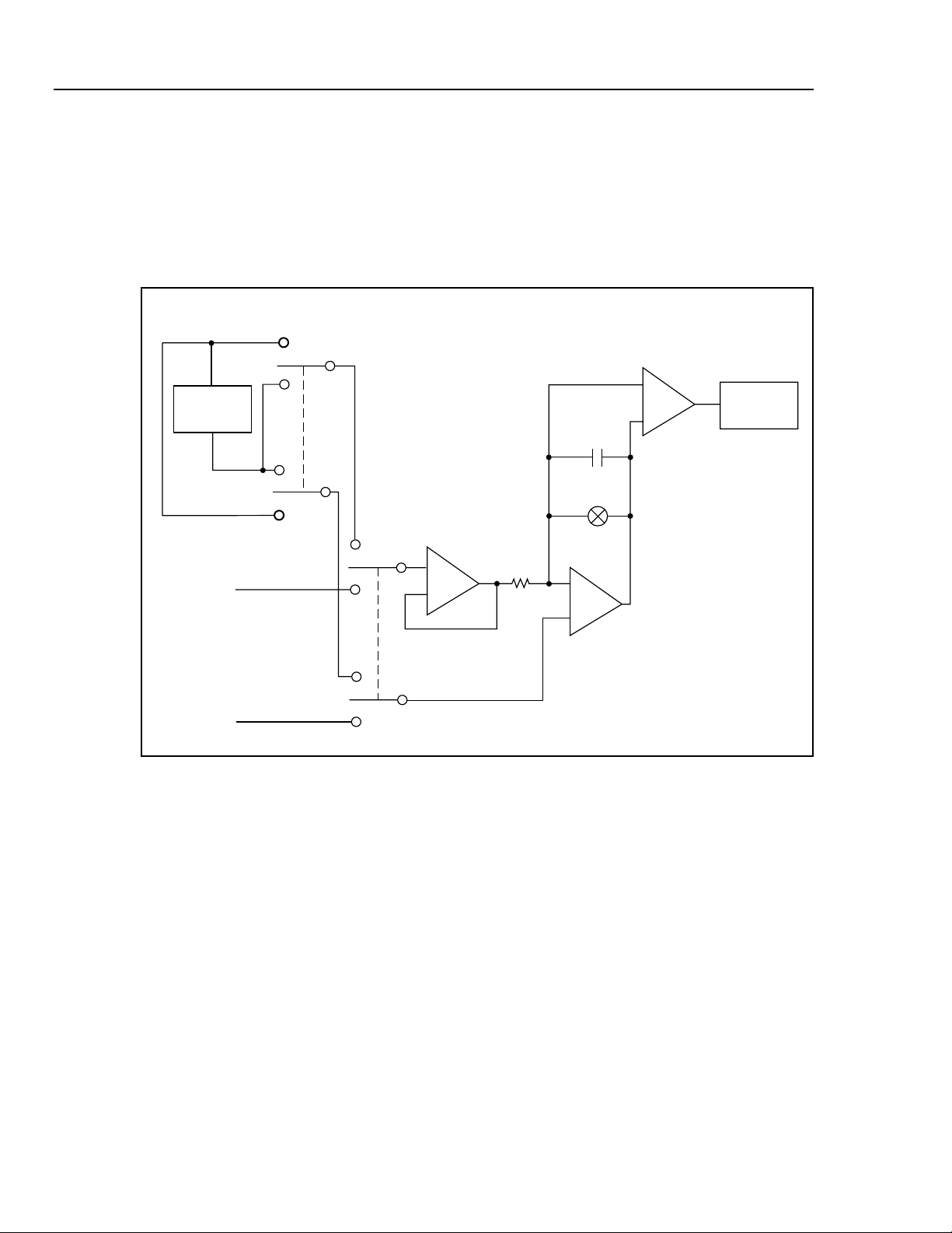
HYDRA
Service Manual
2-59. A/D Converter
Figure 2-7 shows the dual slope a/d converter used in the instrument. The unknown input
voltage is buffered and used to charge (integrate) a capacitor for an exact period of time.
This integrator capacitor is then discharged by the buffered output of a stable and
accurate reference voltage of opposite polarity. The capacitor discharge time, which is
proportional to the level of the unknown input signal, is measured by the digital circuits
in the Analog Measurement Processor. This time count becomes the conversion result.
+ REFERENCE
(– INPUT)
+
REFERENCE
_
INPUT HI
INPUT LO
–REFERENCE
(+ INPUT)
INTEGRATE
REFERENCE
INTEGRATE
INPUT
+
_
BUFFER
A3Z2
A3C13
S77
_
+
INTEGRATOR
+
COUNTER
_
A/D
COMPARATOR
Figure 2-7. A/D Converter Simplified Schematic
In both the slow and fast measurement rates, the a/d converter uses its ±300 mV range
for most measurement functions and ranges. The primary exceptions are that the 3V dc
range is measured on the a/d converter 3V range, thermocouples are measured on the
±100 mV range, and the temperature reference is measured on the 1V a/d converter
range. The typical overload point on a slow rate 30000 count range is 32000 display
counts; the typical overload point on a fast rate 3000 count range is 3200 display counts.
s7f.eps
2-26
During the integrate phase, the a/d buffer in the A3U8 Analog Measurement Processor
applies the signal to be measured to one of the four integrator input resistors in network
A3Z2. As shown on the A/D Converter schematic diagram in Section 8, the choice of
resistor selects the a/d converter range. Switch S69 connects the buffer output through
pin B.1 for the 100-mV range, S71 connects the output through B.32 for the 300 mV
range, S73 connects to pin B1 for the 1V range, and S75 sets up the 3V range through
pin B3.2.
Page 75

The current through the selected integrator input resistor charges integrator capacitor
A3C13, with the current dependent on the buffer output voltage. After the integrate
phase, the buffer is connected to the opposite polarity reference voltage, and the
integrator integrates back toward zero capacitor voltage until the comparator trips. An
internal counter measures this variable integrate time. If the a/d converter input voltage
is too high, the integrator overloads and does not return to its starting point by the end of
the measurement phase. Switch S77 is then turned on to discharge integrate capacitor
A3C13.
The reference voltage used during the variable integrate period for voltage (and high
ohms) conversions is generated from zener reference diode A3VR1, which is time and
temperature stable. The reference amplifier in the Analog Measurement Processor, along
with resistors A3R15, A3R18, and A3R21, pulls approximately 2 mA of current through
the zener. Resistors in network A3Z2 divide the zener voltage down to the reference
1.05V required by the A/D Converter.
2-60. Inguard Microcontroller Circuitry
The Microcontroller, A3U9, with its internal program memory and RAM and associated
circuitry, controls measurement functions on the A/D Converter PCA and communicates
with the Main (outguard) processor.
Theory of Operation (2620A/2625A)
Detailed Circuit Description
2
The Microcontroller communicates directly with the A3U8 Analog Measurement
Processor using the CLK, CS, AR, and AS lines and can monitor the state of the analog
processor using the FC[0:7] lines. Filter zeroing is controlled by the ZERO signal. The
open thermocouple detect circuitry is controlled by the OTCCLK and OTCEN lines and
read by the OTC line. The Microcontroller also communicates with the Main (outguard)
processor serially using the IGDR line to receive and the IGDS line (driven by A3Q1) to
send.
The channel and function relays are driven to the desired measurement state by signals
sent out through microcontroller ports 1, 3, 4, 6, and 7.
On power up, the reset/break detect circuit made up of quad comparator A3U1,
capacitors A3C1 and A3C2, and resistors A3R1 through A3R6 and A3R8 resets the
Microcontroller through the RESET* line. When a break signal is received from the
outguard processor, the inguard A3U9 is again reset. Therefore, if Microcontroller
operation is interrupted by line transients, the outguard can regain control of the inguard
by resetting A3U9.
2-61. Channel Selection Circuitry
Measurement input channel selection is accomplished by a set of latching 4-form-C
relays organized in a tree structure. Relays A3K5, A3K6, and A3K8 through A3K14
select among channels 1 through 20. Relay A3K7 disconnects rear input channels 1
through 20 from the measurement circuitry between measurements. Relay A3K3
switches in the front panel channel 0 or the rear channels. Inductors A3L1 through
A3L24 reduce EMI and current transients.
Selection between 2-wire and 4-wire operation for ohms measurements is performed by
latching 2-form-C relays (A3K1 and A3K2.) These relays also serve to select a voltage
or thermocouple rear input channel from either channels 1 through 10 or channels 11
through 20.
2-27
Page 76

HYDRA
Service Manual
2-62. Open Thermocouple Check
The coils for the relays are driven by the outputs of Darlington drivers A3U4, A3U5,
A3U10, A3U11, and A3U12. The relays are switched when a 6-millisecond pulse is
applied to the appropriate reset or set coil by the NPN Darlington drivers in these ICs.
When the port pin of Microcontroller A3U9 connected to the input of a driver is set high,
the output of the driver pulls one end of a relay set or reset coil low. Since the other end
of the relay coil is connected to the VDDR supply, a magnetic field is generated, causing
the relay armature and contacts to move to (or remain in) the desired position.
Immediately before a thermocouple measurement, the open thermocouple check circuit
applies a small, ac-coupled signal to the thermocouple input. Microcontroller A3U9
initiates the test by asserting OTCEN, causing comparator A3U14/A3R40 to turn on
JFET A3Q12. Next, the Microcontroller sends a 78-kHz square wave out the OTCCLK
line through A3R41, A3Q12, and A3C32 to the thermocouple input. The resulting
waveform is detected by A3U13 and A3CR2, and a proportional level is stored on
capacitor A3C30. Op amp A3U13 compares this detected level with the VTH threshold
voltage set up by A3R37 and A3R36 and stored on A3C29. If the resistance at the input
is too large, the VTH level will be exceeded and the OTC (open thermocouple check)
line will be asserted. After a short delay, the Microcontroller analyzes this OTC signal,
determines whether the thermocouple should be reported as open, and deasserts OTCEN
and sets OTCCLK high, ending the test.
2-63. Input Connector PCA
The Input Connector assembly, which plugs into the A/D Converter PCA from the rear
of the instrument, provides 20 pairs of channel terminals for connecting measurement
sensors. This assembly also provides the reference junction temperature sensor circuitry
used when making thermocouple measurements.
Circuit connections between the Input Connector and A/D Converter PCAs are made via
connectors A4P1 and A4P2. Input channel and earth ground connections are made via
A4P1, while temperature sensor connections are made through A4P2.
Input connections to channels 1 through 20 are made through terminal blocks TB1 and
TB2. Channel 1 and 11 HI and LO terminals incorporate larger creepage and clearance
distances and each have a metal oxide varistor (MOV) to earth ground in order to clamp
voltage transients. MOVs A4RV1 through A4RV4 limit transient impulses to the more
reasonable level of approximately 1800V peak instead of the 2500V peak that can be
expected on 240 VAC, IEC 664 Installation Category II, ac mains. In this way, higher
voltage ratings can be applied to channels 1 and 11 than can be applied to the other rear
channels.
Strain relief for the user’s sensor wiring is provided both by the Connector PCA housing
and the two round pin headers. Each pin of the strain relief headers is electrically
isolated from all other pins and circuitry.
Temperature sensor transistor A4Q1 outputs a voltage inversely proportional to the
temperature of the input channel terminals. This voltage is 0.6V dc at 25ºC, increasing 2
mV with each degree decrease in temperature, or decreasing 2 mV with each degree
increase in temperature. For high accuracy, A4Q1 is physically centered within and
thermally linked to the 20 input terminals. Local voltage reference A4VR1 and resistors
A4R1 through A4R3 set the calibrated operating current of the temperature sensor.
Capacitor A4C1 shunts noise and EMI to ground.
2-28
Page 77

2-64. Display PCA
Display Assembly operation is classified into six functional circuit blocks: the Main
PCA Connector, the Front Panel Switches, the Display, the Beeper Drive Circuit, the
Watchdog Timer/Reset Circuit, and the Display Controller. These blocks are described
in the following paragraphs.
2-65. Main PCA Connector
The 20-pin Main PCA Connector (A2J1) provides the interface between the Main PCA
and the other functional blocks on the Display PCA. Seven of the connector pins provide
the necessary connections to the four power supply voltages (-30V dc, -5V dc, +5.1V dc,
and 5.4V ac filament voltage). Six pins are used to provide the interface to the Front
Panel Switches (A2SWR1 through A2SWR6). The other seven signals interface the
Microprocessor (A1U4) to the Display Controller (A2U1) and pass the reset signals
between the assemblies.
2-66. Front Panel Switches
The Microprocessor scans the 19 Front Panel Switches (A2S1 through A2S18, and
A2S21) using only six interface signals (plus the ground connection already available
from the power supply). These six signals (SWR1 through SWR6) are connected to a
bidirectional I/O port on the microprocessor. Each successive column has one less
switch.
Theory of Operation (2620A/2625A)
Detailed Circuit Description
2
This arrangement allows the unused interface signals to function as strobe signals when
their respective column is driven by the Microprocessor. The Microprocessor cycles
through six steps to scan the complete Front Panel Switch matrix. Table 2-7 shows the
interface signal state and, if the signal state is an output, the switches that may be
detected as closed.
Table 2-7. Front Panel Switch Scanning
Interface Signal States or Key Sensed
Step SWR6 SWR5 SWR4 SWR3 SWR2 SWR1
1 A2S8 A2S17 A2S10 A2S12 A2S18 A2S13
2 A2S1 A2S2 A2S3 A2S4 A2S11 0
3 A2S7 A2S9 A2S5 A2S6 0 Z
4 A2S14 A2S15 A2S16 0 Z Z
5NANA0 Z Z Z
6 A2S21 0 Z Z Z Z
A2Sn indicates switch closure sensed.
0 indicated strobe driven to logic 0
Z indicated high impedance input; state ignored.
In step 1, six port bits are set to input, and the interface signal values are read. In steps 2
through 6, the bit listed as O is set to output zero, the other bits are read, and bits
indicated by a Z are ignored.
Each of the interface signals is pulled up to the +5V dc supply by a 10-kΩ resistor in
network A2Z1. Normally, the resistance between any two of the interface signals is
2-29
Page 78

HYDRA
Service Manual
2-67. Display
2-68. Beeper Drive Circuit
approximately 20 kΩ. Checking resistances between any two signals (SWR1 through
SWR6) verifies proper termination by resistor network A2Z1.
The custom vacuum-fluorescent display (A2DS1) comprises a filament, 11 grids
(numbered 0 through 10 from right to left on the display), and up to 14 anodes under
each grid. The anodes make up the digits and annunciators for their respective area of the
display. The grids are positioned between the filament and the anodes.
A 5.4V ac signal, biased at a -24V dc level, drives the filament. When a grid is driven to
+5V dc, the electrons from the filament are accelerated toward the anodes that are under
that grid. Anodes under that grid that are also driven to +5V dc are illuminated, but the
anodes that are driven to -30V dc are not. Grids are driven to +5V dc one at a time,
sequencing from GRID(10) to GRID(0) (left to right, as the display is viewed.)
The Beeper Drive circuit drives the speaker (A2LS1) to provide an audible response to a
button press. A valid entry yields a short beep; an incorrect entry yields a longer beep.
The circuitry comprises a dual four-bit binary counter (A2U4) and a NAND gate (A2U6)
used as an inverter. One four-bit free-running counter (A2U4) divides the 1.2288-MHz
clock signal (E) from the microprocessor (A1U4) by 2 to generate the 614.4-kHz clock
(CLK1) used by the Display Controller. This counter also divides the 1.2288-MHz clock
by 16, generating the 76.8-kHz clock that drives the second four-bit binary counter
(A2U4).
The second four-bit counter is controlled by an open-drain output on the Display
Controller (A2U1-17) and pull-down resistor A2R1. When the beeper (A2LS1) is off,
A2U1-17 is pulled to ground by A2R1. This signal is then inverted by A2U6, with
A2U6-6 driving the CLR input high to hold the four-bit counter reset. Output A2U4-8 of
the four-bit counter drives the parallel combination of the beeper (A2LS1) and A2R10 to
ground to keep the beeper silent. When commanded by the Main Microprocessor, the
Display Controller drives A2U1-17 high, enabling the beeper and driving the CLR input
of the four-bit counter (A2U4-12) low. A 4.8-kHz square wave then appears at counter
output A2U4-8 and across the parallel combination of A2LS1 and A2R10, causing the
beeper to resonate.
2-69. Watchdog Timer and Reset Circuit
This circuit provides active high and active low reset signals to the rest of the system at a
power-up or system reset if the Microprocessor does not communicate with the Display
Processor for a 5-second period. The Watchdog Timer and Reset Circuit comprises dual
retriggerable monostable multivibrator A2U5, NAND gates A2U6, diode A2CR3, and
various resistive and capacitive timing components.
At power-up, capacitor A2C3 begins to charge up through resistor A2R3. The voltage
level on A2C3 is detected by an input of Schmitt-Trigger NAND gate A2U6-12. The
output of this gate (A2U6-11) then drives the active high reset signal (RESET) to the rest
of the system. When the voltage on A2C3 is below the input threshold (typically +2.5V
dc) of A2U6-12, A2U6-11 is high. As soon as A2C3 charges up to the threshold of
A2U6-12, A2U6-11 goes low. The RESET signal drives NAND gate inputs A2U6-1 and
A2U6-2 to generate the active low reset signal (RESET*) at A2U6-3.
2-30
When the RESET signal transitions from high to low (A2U5-1), the Watchdog Timer is
triggered initially, causing A2U5-13 to go high. This half of the dual retriggerable
monostable multivibrator uses timing components A2R2 and A2C2 to define a nominal
Page 79

4.75-second watchdog timeout period. Each time a low-to-high transition of DISTX is
detected on A2U5-2, capacitor A2C2 is discharged to restart the timeout period. If there
are no low-to-high transitions on DISTX during the 4.75-second period, A2U5-13
transitions from high to low, triggers the other half of A2U5, and causes output A2U5-12
to go low. A2U5-12 is then inverted by A2U6 to drive the RESET signal high, causing a
system reset. The low duration of A2U5-12 is determined by timing components A2Z1
and A2C4 and is nominally 460 µs. When A2U5-12 goes high again, RESET goes low to
retrigger the Watchdog Timer.
2-70. Display Controller
The Display Controller is a four-bit, single-chip microcomputer with high-voltage
outputs that are capable of driving a vacuum-fluorescent display directly. The controller
receives commands over a three-wire communication channel from the Microprocessor
on the Main Assembly. Each command is transferred serially to the Display Controller
on the display transmit (DISTX) signal, with bits being clocked into the Display
Controller on the rising edges of the display clock signal (DSCLK). Responses from the
Display Controller are sent to the Microprocessor on the display receive signal (DISRX)
and are clocked out of the Display Controller on the falling edge of DSCLK.
Series resistor A2R11 isolates DSCLK from A2U1-40, preventing this output from
trying to drive A1U4-16 directly. Figure 2-8 shows the waveforms during a single
command byte transfer. Note that a high DISRX signal is used to hold off further
transfers until the Display Controller has processed the previously received byte of the
command.
Theory of Operation (2620A/2625A)
Detailed Circuit Description
2
DSCLK
BIT 6 BIT 5 BIT 4 BIT 3 BIT 2 BIT 1 BIT 0
DISTX
DISRX
CLEAR TO
RECEIVE
26 µs
BIT 7
BIT 7
BIT 6 BIT 5 BIT 4 BIT 3 BIT 2 BIT 1 BIT 0
Figure 2-8. Command Byte Transfer Waveforms
HOLD OFF
CLEAR TO
RECEIVE
26 µs
Once reset, the Display Controller performs a series of self-tests, initializing display
memory and holding the DISRX signal high. After DISRX goes low, the Display
Controller is ready for communication; on the first command byte from the
Microprocessor, the Display Controller responds with a self-test results response. If all
self-tests pass, a response of 00000001 (binary) is returned. If any self-test fails, a
response of 01010101 (binary) is returned. The Display Controller initializes its display
memory to one of four display patterns depending on the states of the DTEST* (A2U1-
41) and LTE* (A2U1-13) inputs. The DTEST* input is pulled up by A2Z1, but may be
pulled down by jumpering A2TP4 to A2TP3 (GND). The LTE* input is pulled down by
A2R12, but may be pulled up by jumpering A2TP5 to A2TP6 (VCC). The default
conditions of DTEST* and LTE* cause the Display Controller to turn all segments on
bright at power-up.
Table 2-8 defines the logic and the selection process for the four display initialization
modes.
The two display test patterns are a mixture of on and off segments forming a
recognizable pattern that allows for simple testing of display operation. Test patterns #1
and #2 are shown in Section 5 of this manual.
s8f.eps
2-31
Page 80

HYDRA
Service Manual
Table 2-8. Display Initialization Modes
A2TP4 A2TP5 Power-Up Display Initialization
1 1 All Segments OFF
1 0 All Segments ON (default)
0 1 Display Test Pattern #1
0 0 Display Test Pattern #2
The Display Controller provides 11 grid control outputs and 15 anode control outputs
(only 14 anode control outputs are used). Each of these 26 high-voltage outputs provides
an active driver to the +5V dc supply and a passive 220-kΩ (nominal) pull-down to the 30V dc supply. These pull-down resistances are internal to the Display Controller.
The Display Controller provides multiplexed drive to the vacuum-fluorescent display by
strobing each grid while the segment data for that display area is present on the anode
outputs. Each grid is strobed for approximately 1.14 milliseconds every 13.8
milliseconds, resulting in each grid on the display being strobed about 72 times per
second. The grid strobing sequence is from GRID(10) to GRID(0), which results in leftto-right strobing of grid areas on the display. Figure 2-9 shows grid control signal
timing.
The single grid strobing process involves turning off the previously enabled grid,
outputting the anode data for the next grid, and then enabling the next grid. This
procedure ensures that there is some time between grid strobes so that no shadowing
occurs on the display. A grid is enabled only if one or more anodes are also enabled.
Thus, if all anodes under a grid are to be off, the grid is not turned on. Figure 2-10
describes the timing relationship between an individual grid control signal and the anode
control signals.
GRID(10)
GRID(9)
…
…
GRID(1)
GRID(0)
GRID TIMING
13.8 ms
0V
1.14 ms
0V
1.14 ms
0V
1.14 ms
0V
1.14 ms
116 µs
s9f.eps
Figure 2-9. Grid Control Signal Timing
2-32
Page 81
Theory of Operation (2620A/2625A)
Detailed Circuit Description
GRID/ANODE TIMING
5V
0V
2
GRID(X)
-30V
5V
0V
ANODE(14..0)
-30V
GRID(X-1)
-30V
5V
0V
19 µs
60 µs
Figure 2-10. Grid-Anode Timing Relationships
2-71. Memory PCA (2625A Only)
The Memory PCA is a serially-accessed, byte-wide, nonvolatile 256K-byte memory that
is capable of storing up to 2047 scans of data. The following paragraphs describe in
detail the Main PCA Connector, Address Decoding, Page Register, Byte Counter, and
Nonvolatile Memory blocks that make up this assembly.
1.14 ms
116 µs
56 µs
98 µs
s10f.eps
2-72. Main PCA Connector
The Memory PCA interfaces to the Main PCA through a 26-pin, right angle connector
(A6J1). This connector routes the eight-bit data bus, the lower three bits of the address
bus, memory control and address decode signals from the Main PCA to the Memory
PCA. The Memory PCA is powered by the +5.1V dc power supply (VCC). The Memory
PCA is sensed by the Microprocessor on the Main PCA through the connection of A6J111 to the option sense signal OPS* (A6J1-22).
2-73. Address Decoding
Circuitry on the Main PCA decodes the Microprocessor address bus and provided the
MEM* select signal to the Memory PCA. The 3-line to 8-line decoder (A6U8) is used to
decode the three least significant address bits to get register select signals for
hexadecimal addresses 4, 5, and 6. When the MEM* signal drives A6U8-4 low and the
RESET* signal (A6U8-6) is high, the A0 through A2 address bits are decoded to get the
MEMORY, PAGEL, and PAGEH register select signals.Address decoding is disabled
when RESET* is low so that the Nonvolatile Memory cannot be accidentally modified
during power-up or power-down.
2-74. Page Register
The Page Register is an 11-bit register that is writable by the Microprocessor on the
Main PCA. The outputs of this register control the most significant address bits of the
nonvolatile memories (A6U6 and A6U7.) When register select PAGEL goes high and
2-33
Page 82

HYDRA
Service Manual
2-75. Byte Counter
2-76. Nonvolatile Memory
the WE* signal is low, NAND gate output A6U2-3 goes high to latch the data bus into
the lower part of the page register (A6U1).When register select PAGEH goes high and
the WE* signal is low, NAND gate output A6U2-8 goes high to latch the lower three bits
of the data bus into the high part of the page register (A6U4).
The Byte Counter is a seven-bit ripple counter that controls the lower address bits of the
nonvolatile RAMs. This counter is cleared when a new value is written to the lower page
register. It automatically increments at the end of each read or write access to the
memory data register.
NAND gate output A6U2-3 goes high to write the lower page register and clear the Byte
Counter. When data is read from or written to the Non-Volatile Memory, NAND gate
output A6U2-6 goes high during the memory cycle, and then low at the end of the
memory cycle. The transition from high to low increments the Byte Counter so that the
next access to the memory data register will be for the next sequential byte in the NonVolatile Memory.
The Non-Volatile Memory is made up of two 128K-byte static CMOS memories with
integrated lithium battery, power-fail detection, and battery switching circuitry. When
the VCC (+5.1V dc) power supply is above +4.5V dc, memories A6U6 and A6U7 are
fully operational. When VCC drops below approximately +4.25V dc, all access to the
memory are disabled by the internal power-fail detection circuit. When VCC drops
below about +3.0V dc, the battery switching circuitry disconnects VCC and connects the
lithium battery to the memory so that data is retained while the instrument power is off.
The most significant bit of the Page Register (A6U4-1,16) is gated with the MEMORY
register select signal by A6U5 to get the memory chip select signals (A6U5-6 and
A6U5-8). Memory pages 0 through 1023 are stored in memory device A6U7, and
memory pages 1024 through 2047 are stored in memory device A6U6. The WR* and
RD* control signals from the Microprocessor on the Main PCA are used to enable
writing of data to and reading data from the memory devices, respectively.
2-34
2-77. IEEE-488 Interface (Option -05)
Refer to Section 7 for detailed circuit description of this option.
Page 83

Chapter 2A
Theory of Operation (2635A)
Title Page
2A-1. Introduction..........................................................................................2A-3
2A-2. Functional Block Description...............................................................2A-3
2A-3. Main PCA Circuitry.........................................................................2A-3
2A-4. Power Supply...............................................................................2A-3
2A-5. Digital Kernel..............................................................................2A-3
2A-6. Serial Communication (Guard Crossing)....................................2A-6
2A-7. Digital Inputs and Outputs...........................................................2A-6
2A-8. A/D Converter PCA.........................................................................2A-6
2A-9. Analog Measurement Processor..................................................2A-6
2A-10. Input Protection Circuitry............................................................2A-6
2A-11. Input Signal Conditioning............................................................2A-6
2A-12. Analog-to-Digital (A/D) Converter.............................................2A-6
2A-13. Inguard Microcontroller Circuitry...............................................2A-6
2A-14. Channel Selection Circuitry.........................................................2A-7
2A-15. Open Thermocouple Check Circuitry..........................................2A-7
2A-16. Input Connector Assembly...............................................................2A-7
2A-17. 20 Channel Terminals..................................................................2A-7
2A-18. Reference Junction Temperature.................................................2A-7
2A-19. Display PCA ....................................................................................2A-7
2A-20. Memory Card Interface PCA...........................................................2A-7
2A-21. Detailed Circuit Description ................................................................2A-7
2A-22. Main PCA ........................................................................................2A-7
2A-23. Power Supply Circuit Description...............................................2A-8
2A-31. Digital Kernel..............................................................................2A-10
2A-42. Digital I/O....................................................................................2A-19
2A-43. Digital Input Threshold ...............................................................2A-19
2A-44. Digital Input Buffers....................................................................2A-19
2A-45. Digital and Alarm Output Drivers...............................................2A-19
2A-1
Page 84

HYDRA
Service Manual
2A-46. Totalizer Input .............................................................................2A-19
2A-47. External Trigger Input Circuits....................................................2A-20
2A-48. A/D Converter PCA.........................................................................2A-20
2A-49. Analog Measurement Processor..................................................2A-20
2A-50. Input Protection ...........................................................................2A-24
2A-51. Input Signal Conditioning............................................................2A-25
2A-57. Passive and Active Filters............................................................2A-30
2A-58. A/D Converter .............................................................................2A-30
2A-59. Inguard Microcontroller Circuitry...............................................2A-32
2A-60. Channel Selection Circuitry.........................................................2A-32
2A-61. Open Thermocouple Check.........................................................2A-32
2A-62. Input Connector PCA.......................................................................2A-33
2A-63. Display PCA ....................................................................................2A-33
2A-64. Main PCA Connector ..................................................................2A-33
2A-65. Front Panel Switches...................................................................2A-34
2A-66. Display.........................................................................................2A-34
2A-67. Beeper Drive Circuit....................................................................2A-34
2A-68. Watchdog Timer and Reset Circuit.............................................2A-35
2A-69. Display Controller .......................................................................2A-35
2A-70. Memory Card Interface PCA...........................................................2A-37
2A-71. Main PCA Connector ..................................................................2A-38
2A-72. Microprocessor Interface.............................................................2A-38
2A-73. Memory Card Controller.............................................................2A-38
2A-74. PCMCIA Memory Card Connector.............................................2A-39
2A-2
Page 85

2A-1. Introduction
The theory of operation begins with a general overview of the instrument and progresses
to a detailed description of the circuits of each pca.
The instrument is first described in general terms with a Functional Block Description.
Then, each block is detailed further (often to the component level) with Detailed Circuit
Descriptions. Refer to Section 8 of this manual for full schematic diagrams. The
Interconnect Diagram in this section (Figure 2A-1) illustrates physical connections
among pca’s.
Signal names followed by a ’*’ are active (asserted) low. All other signals are active high.
2A-2. Functional Block Description
Refer to Figure 2A-2, Overall Functional Block Diagram, during the following
functional block descriptions.
2A-3. Main PCA Circuitry
The following paragraphs describe the major circuit blocks on the Main PCA.
Theory of Operation (2635A)
Introduction
2A
2A-4. Power Supply
The Power Supply functional block provides voltages required by the vacuumfluorescent display (-30V dc, -5.0V dc, and filament voltage of 5.4V ac), the inguard
circuitry (-5.4V dc VSS, +5.3V dc VDD, and +5.6V dc VDDR), and outguard digital
circuitry of +5.0V dc (VCC).
Within the Power Supply, the Raw DC Supply converts ac line voltage to dc levels. The
5V Switching Supply converts this raw dc to 5.0V ±0.25V dc, which is used by the
Inverter in generating the above-mentioned outputs. The Power Fail Detector monitors
the Raw DC Supply and provides a power supply status signal to the Microprocessor in
the Digital Kernel.
2A-5. Digital Kernel
The Digital Kernel functional block is responsible for the coordination of all activities
within the instrument. This block requires voltages from the Power Supply and signals
from the Power-on Reset circuit.
Specifically, the Digital Kernel Microprocessor performs the following functions:
• Executes the instructions stored in FLASH EPROM.
• Stores temporary data and nonvolatile instrument configuration datain NVRAM.
• Stores instrument calibration data in FLASH EPROM.
• Communicates with the microcontroller on the A/D Converter PCA viathe Serial
Communication (Guard Crossing) block.
• Communicates with the Display Controller to display readings and userinterface
information.
• Communicates with the Field Programmable Gate Array, which scans theuser
interface keyboard found on the Display Assembly and interfaceswith the Digital I/O
hardware.
• Communicates with a host computer via the RS-232 interface.
• Stores instrument setup and measurement data on a Static RAM memorycard
installed in the Memory Card Interface Assembly.
• Reads the digital inputs and changes digital and alarm outputs.
2A-3
Page 86

HYDRA
Service Manual
DIGITAL I/O AND
TOTALIZE INPUT
ALARM OUTPUTS
SCAN TRIGGER INPUT
AC IN
RS-232
J3J5J6J4
CHANNELS 11…20
DISPLAY
MEMORY
CRAD
INTERFACE
J1
P2
J2
MAIN
P4
P10
CHANNEL 0
2A-4
CHANNELS 1…10
TB1
TB2
ANALOG
INPUT
CONNECTOR
P1
P2 J2
J1
FIGURE 2A-1. InterconnectDiagram (2635A)
J10
A/D
CONVERTER
S11F.EPS
Page 87

ANALOG INPUT CONNECTOR
INPUT MULTIPLEXING
INPUT PROTECTION
INPUT SIGNAL
CONDITIONING
ANALOG
MEASUREMENT
PROCESSOR
(A/D CONVERTER)
Theory of Operation (2635A)
Functional Block Description
2A
INGUARD
OUTGUARD
VACUUM FLUORESCENT
DISPLAY
DISPLAY CONTROLLER
FRONT PANEL SWITCHES
DISPLAY ASSEMBLY
MICRO CONTROLLER
SERIAL
COMMUNICATION
µ
P
FPGA
POWER
SUPPLY
FLASH
MEMORY
ADDRESS
DECODING
+5.6 Vdc (V
–5.4 Vdc (VSS)
+5.3Vdc (V
NVRAM &
REAL-TIME
CLOCK
RESET
CIRCUITS
)
DDR
)
DD
A/D CONVERTER
PCA
GUARD
CROSSING
RS-232
MEMORY
CARD
INTERFACE
OPTION
INTERFACE
DIGITAL I/O
INGUARD
MAIN PCA
–30 Vdc (V
+5.1 Vdc (VCC)
–5 Vdc (VEE)
5.4 Vac
LOAD
)
OUTGUARD
Figure 2A-2. Overall Functional Block Diagram (2635A)
s12f.eps
2A-5
Page 88

HYDRA
Service Manual
2A-6. Serial Communication (Guard Crossing)
2A-7. Digital Inputs and Outputs
2A-8. A/D Converter PCA
2A-9. Analog Measurement Processor
This functional block provides a high isolation voltage communication path between the
Digital Kernel of the Main PCA and the microcontroller on the A/D Converter PCA.
This bidirectional communication circuit requires power supply voltages from the Power
Supply block.
This functional block contains the Totalizer and External Trigger Input Buffers, eight
bidirectional Digital I/O channels, four Alarm Outputs, and the Input Threshold control
circuits. These circuits require power supply voltages from the Power Supply and signals
from the Digital Kernel.
The following paragraphs describe the major blocks of circuitry on the A/D Converter
PCA.
The Analog Measurement Processor (A3U8) provides input signal conditioning, ranging,
a/d conversion, and frequency measurement. This custom chip is controlled by the A/D
Microcontroller (A3U9). The A/D Microcontroller communicates with the Main PCA
Microprocessor (A1U1) over a custom serial interface.
2A-10. Input Protection Circuitry
This circuitry protects the instrument measurement circuits during overvoltage
conditions.
2A-11. Input Signal Conditioning
Here, each input is conditioned and/or scaled to a dc voltage for measurement by the a/d
converter. DC voltage levels greater than 3V are attenuated. To measure resistance, a dc
voltage is applied across a series connection of the input resistance and a reference
resistance to develop dc voltages that can be ratioed. DC volts and ohms measurements
are filtered by a passive filter. AC voltages are first scaled by an ac buffer, converted to a
representative dc voltage by an rms converter, and then filtered by an active filter.
2A-12. Analog-to-Digital (A/D) Converter
The dc voltage output from the signal conditioning circuits is applied to a
buffer/integrator which charges a capacitor for an exact amount of time. The time
required to discharge this capacitor, which is proportional to the level of the unknown
input signal, is then measured by the digital counter circuits in the Analog Measurement
Processor.
2A-13. Inguard Microcontroller Circuitry
This microcontroller (and associated circuitry) controls all functions on the A/D
Converter PCA and communicates with the digital kernel on the Main PCA. Upon
request by the Main PCA, the inguard microcontroller selects the input channel to be
measured through the channel selection circuitry, sets up the input signal conditioning,
commands the Analog Measurement Processor to begin a conversion, stops the
measurement, and then fetches the measurement result. The inguard microcontroller
manipulates the result mathematically and transmits the reading to the digital kernel.
2A-6
Page 89

2A-14. Channel Selection Circuitry
This circuitry consists of a set of relays and relay-control drivers. The relays form a tree
that routes the input channels to the measurement circuitry. Two of the relays are also
used to switch between 2-wire and 4-wire operation.
2A-15. Open Thermocouple Check Circuitry
Under control of the Inguard Microcontroller, the open thermocouple check circuit
applies a small ac signal to a thermocouple input before each measurement. If an
excessive resistance is encountered, an open thermocouple input condition is reported.
2A-16. Input Connector Assembly
The following paragraphs briefly describe the major sections of the Input Connector
PCA, which is used for connecting most of the analog inputs to the instrument.
2A-17. 20 Channel Terminals
Twenty HI and LO terminal blocks are provided in two rows, one for channels 1 through
10 and one for channels 11 through 20. The terminals can accommodate a wide range of
wire sizes. The two rows of terminal blocks are maintained very close to the same
temperature for accurate thermocouple measurements.
Theory of Operation (2635A)
Detailed Circuit Description
2A
2A-18. Reference Junction Temperature
A semiconductor junction is used to sense the temperature of the thermocouple input
terminals. The resulting dc output voltage is proportional to the block temperature and is
sent to the A/D Converter PCA for measurement.
2A-19. Display PCA
The Display Assembly controller communicates with the main Microprocessor over a
three-wire communication channel. Commands from the Microprocessor inform the
Display Controller how to modify its internal display memory. The Display Controller
then drives the grid and anode signals to illuminate the required segments on the
Display. The A2 Display Assembly requires power supply voltages from the Power
Supply, a reset signal from the Reset Circuit, and a clock signal from the Digital Kernel.
2A-20. Memory Card Interface PCA
The Memory Card Interface PCA is used to access the memory on an industry standard
memory card installed through the slot in the front panel of the instrument. This
assembly allows management of the memory card power, adapts timing of accesses by
the Digital Kernel to the memory card, and provides visible indicators for low battery
voltage and memory card busy status.
2A-21. Detailed Circuit Description
2A-22. Main PCA
>The following paragraphs describe the operation of the circuits on the Main PCA. The
schematic for this pca is located in Section 8.
2A-7
Page 90

HYDRA
Service Manual
2A-23. Power Supply Circuit Description
2A-24. Raw DC Supply
The Hydra power supply consists of three major sections:
• Raw DC Supply
The raw dc supply converts line voltage (90V to 264V ac) to a dcoutput of 7.5V to
35V.
• 5V Switcher Supply
The 5V switching supply regulates the 7.5 to 35V dc input to anominal 5.0V ±0.25V
dc (VCC).
• Inverter
Using the 5V switching supply output, the inverter generates the -30Vdc, -5V dc,
and 5.4V ac supply levels needed for thevacuum-fluorescent display and the RS-232
Interface. The inverteralso provides isolated +5.3V (VDD), +5.6V (VDDR), and -
5.4V (VSS)outputs for the inguard circuitry.
The raw dc supply circuitry receives input from power transformer T401, which operates
on an input ranging from 90V to 264V ac. The power transformer is energized whenever
the power cord is plugged into the ac line; there is no on/off switch on the primary side
of the transformer. The transformer has an internal 275V ac metal-oxide varistor (MOV)
to clamp line transients. The MOV normally acts as an open circuit. When the peak
voltage exceeds approximately 400V, the line impedance in series with the line fuse
limits transients to approximately 450V. All line voltages use a slow blow 0.125 A,
250V fuse.
On the secondary side of the transformer, rectifiers A1CR2, A1CR3, and capacitor A1C7
rectify and filter the output. When it is ON, switch A1S1 (the front panel POWER
switch) connects the output of the rectifiers to the filter capacitor and the rest of the
instrument. Depending on line voltage, the output of the rectifiers is between 7.5 and
35V dc. Capacitor A1C2 helps to meet electromagnetic interference (EMI) and
electromagnetic compatibility (EMC) requirements.
When external dc power is used, the power switch connects the external dc source to
power the instrument. The external dc input uses thermistor A1RT1 (for overcurrent
protection) and diode A1CR1 (for reverse input voltage protection.) Capacitor A1C59
helps meet EMI/EMC requirements. Resistor A1R48, capacitors A1C2 and A1C39 also
ensure that the instrument meets EMI/EMC performance requirements.
2A-25. Auxiliary 6V Supply
Three-terminal regulator A1U19, voltage-setting resistors A1R44 and A1R46, and
capacitor A1C34 make up the auxiliary 6-volt supply. This supply is used for the inverter
oscillator, inverter driver, and the power fail detection circuits.
2A-26. 5V Switcher
The 5V switcher supply uses a switcher supply controller/switch device A1U9 and
related circuitry.The 7.5V dc to 35V dc input is regulated to 5.1V dc (VCC) through
pulse-width modulation at a nominal switching frequency of 100 kHz.
2A-8
Page 91

Theory of Operation (2635A)
Detailed Circuit Description
The output voltage of the switcher supply is controlled by varying the duty cycle (ON
time) of the switching transistor in the controller/switch device A1U9. A1U9 contains
the supply reference, oscillator, switch transistor, pulse-width modulator comparator,
switch drive circuit, current-limit comparator, current-limit reference, and thermal limit.
Dual inductor A1T2 regulates the current that flows from the raw supply to the load as
the switching transistor in A1U9 is turned on and off. Complementary switchA1CR10
conducts when the switching transistor is off.
The pulse-width modulator comparator in A1U9 compares the output to the reference
and sets the ON-time/OFF-time ratio to regulate the output to 5.1V dc. A1C26 is the
input filter capacitor, and A1C14 is the output filter capacitor. Proper inductor and
capacitor values set the filter frequency response to ensure best overall system stability.
Circuitry consisting of A1R26, A1C21, and A1C18 ensure that the switcher supply
remains stable and operating in the continuous mode. Resistors A1R30 and A1R31 set
the output voltage to within 5% of 5.1V.Capacitor A1C21 sets the operating frequency
of the switcher at approximately 100 kHz.
Resistors A1R30 and A1R31 form a voltage divider that operates in conjunction with
amplifier A1U28, which is configured as a voltage follower.A1U28-5 samples the 5.1V
dc output, while A1U28-6 is the voltage divider input.The effect is to maintain the
junction of R30 and R31 at 5.1V dc, resulting in an A1U28-7 output level of 6.34V dc,
or 1.24V dc above the output.This feedback voltage is applied to A1U9-2, which A1U9
interprets as 1.24V dc because A1U9-3 (ground) is connected to the 5.1V dc output.
2A
A1U9 maintains the feedback and reference voltages at 1.24V dc and thus regulates the
5.1V dc source.
2A-27. Inverter
The inverter supply uses a two transistor driven push-pull configuration. The center tap
of transformer A1T1 primary is connected to the 5.0V dc VCC supply, and each side is
alternately connected to common through transistors A1Q7 and A1Q8. A1R38 may be
removed to disable the inverter supply for troubleshooting purposes. A1Q7 and A1Q8
are driven by the outputs of D flip-flop A1U22. Resistors A1R34 and A1R28, and diodes
A1CR11 and A1CR12 shape the input drive signals to properly drive the gate of the
transistors. D flip-flop A1U22 is wired as a divide-by-two counter driven by a 110-kHz
square wave. The 110-kHz square wave is generated by hex inverter A1U23, which is
connected as an oscillator with a frequency determined by the values of resistors A1R40
and A1R47 and capacitor A1C35. The resulting ac voltage produced across the
secondary of A1T1 is rectified to provide the input to the inverter inguard and outguard
supplies.
2A-28. Inverter Outguard Supply
The inverter outguard supply provides three outputs: 5.4V ac, -30V dc, and -5V dc.
These voltages are required by the display and RS-232 drivers and receiver. The 5.4V ac
supply comes off the secondary windings (pins 6 and 7) on transformer T1, and it is
biased at -24V dc with zener diode A1VR3 and resistor A1R22. Dual diodes A1CR8 and
A1CR9 and capacitor A1C17 are for the -30V dc supply. Capacitors A1C30 and A1C31,
and dual diodes A1CR13 form a voltage doubler circuit that generates -12 volts. Threeterminal regulator A1U18 then regulates this voltage down to -5V for the RS-232 circuit.
Capacitor A1C32 is needed for transient response performance of the three-terminal
regulator.
2A-9
Page 92

HYDRA
Service Manual
2A-29. Inverter Inguard Supply
The inverter inguard supply provides three outputs: +5.3V dc (VDD) and -5.4V dc
(VSS) for the inguard analog and digital circuitry, and +5.6V dc (VDDR) for the relays.
Diodes A1CR5 and A1CR6, and capacitor A1C12 are for the +9.5 volt source, and
diodes A1CR7 and capacitor A1C13 are for the -9.5V source.
Three-terminal regulator A1U6 regulates the 9.5V source to 5.6V for the relays. A1R5
and A1R6 set the output voltage at 5.6V. A1C6 is required for transient performance.
The +5.3V regulator circuit uses A1Q2 for the series-pass element and A1Q4 as the error
amplifier. A1VR2 is the reference for the positive supply. A1R14 provides the current to
bias the reference zener. A1C4 is the output filter, and A1C9 provides frequency
compensation of the regulator circuit. Transistor A1Q1 and resistor A1R13 make up the
current-limit circuit.
When the voltage across A1R13 increases enough to turn on A1Q1, output current is
limited by removing the base drive to A1Q2.
The -5.4 volt regulator operates like the +5.3 volt regulator, except that the NPN
transistors in the positive supply are PNP transistors in the negative supply, and the PNP
transistors in the positive supply are NPN transistors in the negative supply. If a VDDto-VSS short circuit occurs, diode A1CR4 ensures that current limit occurs at the limit
set for the -5.4V dc or +5.3V dc supply, whichever is lower.
2A-30. Power Fail Detection
The power fail detection circuit generates a signal to warn the Microprocessor that the
power supply is going down. A comparator in A1U10 compares the divided-down raw
supply voltage to a voltage reference internal to A1U10. When the raw supply voltage is
greater than about 8V dc, the output of A1U10 is "high" and when the raw supply falls
below 8V dc, the output goes "low". Resistors A1R19 and A1R20 make up the divider,
and capacitor A1C74 provides filtering of high frequency noise at the comparator input.
The reference voltage internal to A1U10 is nominally 1.3 volts dc.
2A-31. Digital Kernel
The Digital Kernel is composed of the following nine functional circuit blocks: the Reset
Circuits, the Microprocessor, the Address Decoding, the Flash Memory, the Nonvolatile
Static RAM and Real-Time Clock, the FPGA (Field Programmable Gate Array), the
Serial Communication (Guard Crossing), the RS-232 Interface, and the Option Interface.
2A-32. Reset Circuits
The Power-On Reset signal (POR*, A1U10-7) is generated by the Microprocessor
Supervisor, which monitors the voltage of VCC at A1U10-2. If VCC is less than +4.65
volts, then A1U10-7 will be driven low. POR* drives the enable inputs of the four tristate buffers in A1U2, causing the HALT*, RESET*, ORST*, and DRST* signals to be
driven low when POR* is low. When POR* goes high, the tri-state buffer outputs
(A1U2) go to their high-impedance state and the pull-up resistors pull the outputs to a
high level.
2A-10
When HALT* and RESET* are both driven low, the Microprocessor (A1U1) is reset and
will begin execution when they both go high. The Microprocessor may execute a "reset"
instruction during normal operation to drive A1U1-92 low for approximately 10
microseconds to reset all system hardware connected to the RESET* signal.
Page 93

The Display Reset signal (DRST*) is driven low by A1U2-6 when POR* is low, or it
may be driven low by the Microprocessor (A1U1-56) if the instrument firmware needs to
reset only the display hardware. For example, the firmware resets the display hardware
after the FPGA is loaded at power-up and the Display Clock (DCLK) signal from the
FPGA begins normal operation. This ensures that the Display Processor is properly reset
while DCLK is active.
The Option Reset signal (ORST*) is driven low by A1U2-3 when POR* is low, or it may
be driven low by the Microprocessor (A1U1-58) if the instrument firmware needs to
reset only the Option Interface hardware. For example, the firmware resets any option
interface hardware after the FPGA is loaded at power-up and the Option Clock (OCLK)
signal from the FPGA begins normal operation. This ensures that any Option Interface
hardware is properly reset while OCLK is active.
2A-33. Microprocessor
The Microprocessor uses a 16-bit data bus and a 19-bit address bus to access locations in
the Flash Memory (A1U14 and A1U16), the Nonvolatile Static RAM (A1U20 and
A1U24), the Real-Time Clock (A1U12), the FPGA (A1U25), the Memory Card
Interface PCA (A6), and the Option Interface (A1J1). All of the data bus lines and the
lowest 12 address lines have series termination resistors located near the Microprocessor
(A1U1) to ensure that the instrument meets EMI/EMC performance requirements. When
a memory access is done to the upper half of the data bus (D15 through D8), the upper
data strobe (UDS*) goes low. When a memory access is done to the lower half of the
data bus (D7 through D0), the lower data strobe (LDS*) goes low. When a memory
access is a read cycle, R/W* must be high. Conversely for any write cycle, R/W* must
be low.
Theory of Operation (2635A)
Detailed Circuit Description
2A
The Microprocessor is a variant of the popular Motorola 68000 processor and is
enhanced by including hardware support for clock generation, address decoding, timers,
parallel ports, synchronous and asynchronous serial communications, interrupt
controller, DMA (Direct Memory Access) controllers, and a watchdog timer.
The 12.288-MHz system clock signal (A1TP11) is generated by the oscillator circuit
composed of A1U1, A1Y1, A1R2, A1C3, and A1C8. This clock goes through a series
termination resistor (A1R107) to the FPGA (A1U25) and also through another series
termination resistor (A1R86) to the Memory Card Interface (A1P4). These resistors are
necessary to ensure that the instrument meets EMI/EMC performance requirements.
The Microprocessor has four software programmed address decoders that include wait
state control logic. These four outputs are used to enable external memory and I/O
components during read and write bus cycles. See "Address Decoding" for a complete
description.
One sixteen-bit timer in the Microprocessor is used to generate a regular interrupt every
53.333 milliseconds. This timer uses the 12.288-MHz system clock (A1TP11) as a clock
source. The timer changes the state of parallel port pin A1U1-113 each time that it
interrupts the Microprocessor. The signal at A1U1-113 should be a 9.375-Hz square
wave (period of 106.67 milliseconds).
Another 16-bit timer is used as the totalizer counter. The totalizer signal originating at
J5-2 goes through the totalizer input buffer, the FPGA, and then to the external clock
input for this timer in the Microprocessor (U1-114 and TP20). See the Totalizer part of
"Digital I/O" for a complete description.
The Microprocessor has two parallel ports. Many of the parallel port pins are either used
as software controlled signals or as inputs or outputs of timers and serial communication
channels. Port A has 16 bits and Port B has 12 bits.
2A-11
Page 94

HYDRA
Service Manual
The Microprocessor communicates to the Display Controller using a synchronous, threewire communication interface controlled by hardware in the Microprocessor.
Information is communicated to the Display Controller to display user interface menus
and measurement data. Details of this communication are described in the Display
Controller Theory of Operation in this section.
The Microprocess communicated to the Microcontroller on the A/D Converter PCA (via
the Serial Communication circuit) using an asynchronous communication channel at
4800 baud. Communication to the Microcontroller (A3U9) originates at A1U1-54.
Communication from the A/D’s Microcontroller to the Microprocessor appears at A1U1-
53. When there is no communication in progress between the Microprocessor and the
Microcontroller, both of these signals are high.
The Microprocessor uses another asynchronous communication channel to communicate
to external computing or modem equipment through the RS-232 interface. This interface
is described in detail in the RS-232 Interface Theory of Operation in this section.
The third asynchronous communication channel in the Microprocessor is connected to
the Option Interface (J1) but is not used in the instrument at this time.
The interrupt controller in the Microprocessor prioritizes interrupts received from
hardware devices both internal and external to the Microprocessor. Table 2A-1 lists
interrupt sources from highest to lowest priority.
Table 2A-1. Microprocessor Interrupt Sources (2635A)
Pin Signal Name Description
A1U1-95 XTINT* External Trigger Interrupt (Highest Priority)
A1U1-96 CINT* Real-Time Clock Interrupt; once per second
A1U1-121 KINT* Keyboard Interrupt; interrupts on each debounced change of keyboard
conditions.
RS-232 Interface Interrupt; internal to the Microprocessor.
A/D Communication Interrupt; internal to the Microprocessor.
Timer Interrupt every 53.333 milliseconds; internal to the Microprocessor.
A1U1-119 MCINT* Memory Card Interface Interrupt; interrupts when a memory card is inserted,
removed, powered up or powered down.
Totalizer Interrupt; internal to the Microprocessor. Interrupts on totalizer
overflow from a count of 65535 to 0.
A1U1-97 OINT* Option Interface Interrupt; not currently used in this product.
The Microprocessor also has several internal DMA (Direct Memory Access) controllers
that are used by the serial communication channels. Each serial communication channel
has a DMA channel that handles character reception and another that handles character
transmission. The use of these DMA controllers is transparent to the external operation
of the Microprocessor, but it is important to understand that communication is handled at
hardware speeds without the need for an interrupt for each character being transferred.
2A-12
A watchdog timer internal to the Microprocessor is programmed to have a 10-second
timeout interval. If the code executed by the Microprocessor fails to reinitialize the
watchdog timer every 10 seconds or less, then A1U1-117 (POR*) is driven low for 16
cycles of SCLK (approximately 1.3 microseconds). This results in a complete hardware
reset of the instrument, which restarts operation.
Page 95

2A-34. Address Decoding
The four chip-select outputs on the Microprocessor are individual software programmed
elements that allow the Microprocessor to select the base address, the size, and the
number of wait states for the memory accessed by each output.
The FLASH* signal (A1U1-128) enables accesses to 128 kilobytes of Flash Memory
(A1U14 and A1U16). The FLASH* signal goes through jumper W3, which must always
be installed during normal instrument operation. W3 is removed only during the initial
programming of the Flash Memory during production at the factory. The SRAM* signal
enables the Nonvolatile Static RAM (A1U20 and A1U24), and the MCARD* signal goes
to the Memory Card Interface PCA (A6). The I/O* signal goes to the I/O Decoder
(A1U11), which decodes small areas of address space for I/O devices like the FPGA, the
Real-Time Clock, and the Option Interface. There are no wait states for accesses to
FLASH* and SRAM*, but two wait states are used for any access to I/O*. Each wait
state adds approximately 83 nanoseconds to the length of a memory read or write cycle.
The Memory Card Interface handles wait state timing for any accesses to MCARD*.
When the Microprocessor is starting up (also referred to as "booting"), the address
decoding maps the address space as shown in Table 2A-2.
Table 2A-2. Booting Microprocessor Memory Map (2635A)
Theory of Operation (2635A)
Detailed Circuit Description
2A
Hexadecimal Address Device Selected
000000 - 03FFFF
100000 - 13FFFF
300000 - 30007F
300080 - 3000FF
300100 - 30017F
310000 - 311FFF
400000 - 401000
Just before beginning execution of the instrument code, the address decoding is changed
to map the address space as shown in Table 2A-3. This change switches the positions of
Flash Memory and Nonvolatile Static RAM within the address space of the
Microprocessor.
Table 2A-3. Instrument Microprocessor Memory Map (2635A)
Hexadecimal Address Device Selected
000000 - 03FFFF
100000 - 13FFFF
300000 - 300007
300008 - 30000F
300010 - 300017
300018 - 30001F (Read Only)
300020 - 300027 (Read Only)
300080 - 3000FF
300100 - 30017F
310000 - 311FFF
400000 - 401000
Flash (A1U14 and A1U16)
NVRAM (A1U20 and A1U24)
FPGA Configuration (A1U25)
Real-Time Clock (A1U12)
Option Interface (A1J1)
Memory Card Interface (A1P4)
Microprocessor Internal
NVRAM (A1U20 and A1U24)
Flash (A1U14 and A1U16)
FPGA Control / Status (A1U25)
Alarm Outputs (A1U25)
Digital Outputs (A1U25)
Digital Inputs (A1U25)
Keyboard Input (A1U25)
Real-Time Clock (A1U12)
Option Interface (A1J1)
Memory Card Interface (A1P4)
Microprocessor Internal
2A-13
Page 96

HYDRA
Service Manual
2A-35. Flash EPROM
The Flash EPROM is an electrically erasable and programmable memory that provides
storage of instructions for the Microprocessor and measurement calibration data.
A switching power supply composed of A1U15, A1T3, A1CR21, and A1C66 through
A1C69 generates a nominal +12 volt programming power supply (VPP) when the
Microprocessor drives VPPEN high (A1U15-2). Resistor A1R35 pulls A1U15-2 to near
ground during power-up to ensure that A1U15 is not enabled while the Microprocessor
is being reset. When the power supply is not enabled, the output voltage (VPP) should be
about 0.1 volt less than the input voltage of the power supply (VCC).
The only time that the programming power supply is active is when new firmware is
being loaded or new calibration constants are being stored into the Flash EPROM. The
code executed immediately after power-up is stored in an area of the Flash EPROM
(known as the Boot Block) that is only eraseable and reprogrammable if BBVPP
(A1U14-30 and A1U16-30) is at a nominal +12 volts. This may be accomplished by
installing jumper A1W1, but this should only be done by a trained technican, and A1W1
should never be installed unless it is necessary to update the Boot firmware. In normal
operation, resistor A1R73 and diode A1CR20 pull BBVPP up to about 0.25 volts less
than VCC.
The FLASH* chip select (A1U1-128) for these devices goes low for any memory access
to A1U14 or A1U16. The FLASH* signal goes through jumper W3, which must always
be installed during normal instrument operation. W3 is removed only during the initial
programming of the Flash Memory during production at the factory. A1U14 is connected
to the high 8 bits of the data bus, so read accesses are enabled by the Read Upper
(RDU*) signal going low, and write accesses are enabled by the Write Upper (WRU*)
signal going low. A1U16 is connected to the low 8 bits of the data bus, so read accesses
are enabled by the Read Lower (RDL*) signal going low, and write accesses are enabled
by the Write Lower (WRL*) signal going low.
2A-36. NVRAM/Real-Time Clock
The Nonvolatile Static RAM (NVRAM) provides the storage of data and configuration
information for the instrument. The Real-Time Clock maintains time and calendar date
information for use by the instrument.
A nonvolatile power supply (VBB) biases A1U12, A1U20, A1U24, and A1U26. The
Microprocessor Supervisor (A1U10) monitors the voltage on VCC (A1U10-2). If VCC
is greater than the voltage of the lithium battery (A1U10-8), A1U10 switches VCC from
A1U10-2 to A1U10-1 (VBB). If VCC drops below the voltage of the lithium battery
(A1U10-8), A1U10 will switch voltage from lithium battery A1BT1 through currentlimiting resistor A1R98 to A1U10-1 (VBB). The nominal current required from the
lithium battery (A1BT1) at room temperature with the instrument powered down is
approximately 2 microamperes. This can be easily measured by checking the voltage
across A1R98.
2A-14
Page 97

Theory of Operation (2635A)
Detailed Circuit Description
The SRAM* address decode output (A1U1-127) for the 128 kilobytes of NVRAM goes
low for any memory access to A1U20 or A1U24. This signal must go through two
NAND gates in A1U26 to the NVRAM chip select inputs (A1U20-22 and A1U24-22).
This ensures that when the instrument is powered down and A1U10-7 is driven low,
A1U20-22 and A1U24-22 will be driven high so that the contents of the NVRAM cannot
be changed and the power dissipated by the NVRAM is minimized. Jumper A1W4 in
A<18> is not used in the current instrument; it should be installed only if more NVRAM
is needed in a future instrument that needs 512 kilobytes of NVRAM using the same
circuit board. A1U24 is connected to the high 8 bits of the data bus, so read accesses are
enabled by the Read Upper (RDU*;A1U24-24) signal going low, and write accesses are
enabled by the Write Upper (WRU*;A1U24-29) signal going low. A1U20 is connected
to the low 8 bits of the data bus, so read accesses are enabled by the Read Lower
(RDL*;A1U20-24) signal going low, and write accesses are enabled by the Write Lower
(WRL*;A1U20-29) signal going low.
Memory accesses to the Real-Time Clock (A1U12) are enabled by the RTC* address
decode output (A1U11-16). This signal must go through two NAND gates in A1U26 to
the Real-Time Clock chip select input (A1U12-18). This ensures that when the
instrument is powered down and A1U10-7 is driven low, A1U12-18 will be driven high
so that the contents of the Real-Time Clock cannot be changed, and the power dissipated
by the Real-Time Clock is minimized. A1U12 is connected to the low 8 bits of the data
bus, so read accesses are enabled by the Read Lower (RDL*;A1U12-19) signal going
low, and write accesses are enabled by the Write Lower (WRL*;A1U12-20) signal going
low. When the instrument is powered up, the accuracy of the timebase generated by the
internal crystal may be tested by measuring the frequency of the 1-Hz square wave
output (A1U12-4). The Real-Time Clock also has an interrupt output (A1U12-3) that is
used by the Microprocessor to time the interval between scans when a scan interval is set
in the instrument. There should be one interrupt per second from the Real-Time Clock.
2A
2A-37. Serial Communication (Guard Crossing)
The transmission of information from the Microprocessor (A1U1) to the Microcontroller
(A3U9) is accomplished via the circuit made up of A1Q10, A1U7, A1R8, A1R16, and
A3R8. The transmit output from the Microprocessor (A1U1-54) is buffered by A1Q10,
which then switches current through optocoupler LED (A1U7-2). Resistor A1R8 limits
the current through the LED.
The phototransistor in A1U7 responds to the light emitted by the LED when A1U1-54 is
driven low. (The collector of the phototransistor, A1U7-5, goes low.) The phototransistor
collector is pulled up by A3R8 on the A/D Converter PCA. When turning off, the
phototransistor base discharges through A1R16. With this arrangement, the rise and fall
times of the phototransistor collector signal are nearly symmetrical.
The transmission of data from the Microcontroller (A3U9) to the Microprocessor
(A1U1) is accomplished via the circuit made up of A3Q1, A3R7, A1U5, A1R7, and
A1R3. The transmit output from the Microcontroller (A3U9-14) is inverted by A3Q1,
which drives the optocoupler LED (A1U5-2) through resistor A3R7. The current through
the LED is limited by resistor A3R7. The phototransistor in A1U5 responds to the light
emitted by the LED when A1U5-2 is driven low. (The collector of the phototransistor,
A1U5-4, goes low.) The phototransistor collector (A1U5-5) is pulled up by resistor
A1R3. When turning off, the phototransistor base discharges through A1R7. With this
arrangement, the rise and fall times of the phototransistor collector signal are nearly
symmetrical.
2A-15
Page 98

HYDRA
Service Manual
2A-38. Display/Keyboard Interface
The Microprocessor sends information to the Display Processor via a three-wire
synchronous communication interface. The detailed description of the DISTX, DISRX,
and DSCLK signals may be found in the detailed description of the Display PCA. Note
that the DISRX signal is pulled down by resistor A1R1 so that Microprocessor inputs
A1U1-49 and A1U1-118 are not floating at any time.
The Display Clock (DCLK) is a 1.024-MHz clock that is generated by the FPGA. Series
resistor A1R85 is necessary to ensure that the instrument meets EMI/EMC performance
requirements. The Display Assembly is reset when the Display Reset (DRST*) signal is
driven low. The reset circuit on the Display Assembly is discharged through resistor
A1R21, which limits the peak current from A2C3. DRST* is driven low at power-up, or
it may be driven low by the Microprocessor (A1U1-56).
The Keyboard interface is made up of six bidirectional I/O lines from the Field
Programmable Gate Array (FPGA). SWR1 through SWR6 (A1U25-67, A1U25-68,
A1U25-71, A1U25-73, A1U25-70, A1U25-69, respectively) are pulled up by A2Z1 on
the Display PCA. Hardware in the FPGA scans the keyboard switch array, detects and
debounces switch changes, and interrupts the Microprocessor to indicate that a
debounced keypress is available. A detailed description of this may be found under the
following heading "Field Programmable Gate Array (FPGA)".
2A-39. Field Programmable Gate Array (FPGA)
The FPGA is a complex programmable logic device that contains the following six
functional elements after the Microprocessor has loaded the configuration into the
FPGA: Clock Dividers, Internal Register Address Decoding, Keyboard Scanner, Digital
I/O Buffers and Latches, Totalizer Debouncing and Mode Selection, and the External
Trigger Logic.
When the instrument is powered up, the FPGA clears its configuration memory and
waits until RESET* (A1U25-78) goes high. The FPGA then tests its mode pins and
should determine that it is in "peripheral" configuration mode (A1U25-54 high; A1U2552 low; A1U25-56 high). In this mode the Microprocessor must load the configuration
information into the FPGA before the FGPA logic can begin operation.
The Microprocessor first makes sure that the FPGA is ready to be configured by driving
XD/P* (A1U25-80) low and then pulsing the RESET* (A1U25-78) input low for about
10 microseconds. The Microprocessor then waits until the XINIT* (A1U25-65) output
goes high, indicating that the FPGA has been initialized and is ready for configuration.
The Microprocessor then writes a byte of configuration data to the FPGA by driving
PGA* (A1U25-88) low and latching the data on the data inputs (D<8> through D<15>)
by pulsing WRU* (A1U25-5) low and then back high. The XRDY (A1U25-99) output
then goes low to indicate that the FPGA is busy loading that configuration byte. The
Microprocessor will then wait until XRDY goes high again before loading the next
configuration byte, and the sequence is repeated until the last byte is loaded. While the
configuration data is being loaded, the FPGA drives the XD/P* signal (A1U25-80) low.
When the FPGA has been completely configured, the XD/P* signal is released and
pulled high by resistor A1R70. The Microprocessor will repeat the configuration
sequence if XD/P* (A1U25-80) does not go high when it is expected to.
2A-16
Page 99

Clock Dividers
The 12.288-MHz system clock (A1U25-30) is divided down by the Clock Dividers to
create the 3.072-MHz Option Clock (OCLK; A1U25-22) and 1.024-MHz Display Clock
(DCLK; A1U25-19). The Display Clock is not a square wave; it is low for 2/3 of a cycle
and high for the other 1/3. The Display Clock is also used internal to the FPGA to create
the 128-kHz Totalizer Debouncer Clock and the 4-kHz Keyboard Scanner Clock.
Internal Register Address Decoding
The FPGA logic decodes four bits of the address bus (A<3> through A<6>), the PGA*
chip select signal (A1U25-88), RDU* (A1U25-95), and WRU* (A1U25-5) to allow the
Microprocessor to read five registers and write to three registers implemented in the
FPGA logic. The absolute addresses are listed in Table 2A-1.
Keyboard Scanner
The Keyboard Scanner sequences through the array of switches on the Display Assembly
to detect and debounce switch closures. After a switch closure is detected, it must remain
closed for at least 16 milliseconds before the Microprocessor will be interrupted and the
Keyboard Input register will be read from the FPGA. When the keyboard interrupt
(KINT*, A1U25-62) goes low, the Keyboard Scanner stops scanning until the
Microprocessor reads the Keyboard Input register which automatically clears the
interrupt by driving KINT* high again. The FPGA will interrupt the Microprocessor
again when the switch on the Display Assembly is detected as open again. Actually the
Microprocessor will be interrupted once for each debounced change in the contents of
the Keyboard Input register. See also the information on "Front Panel Switches" in the
"Display PCA" section for this instrument.
Theory of Operation (2635A)
Detailed Circuit Description
2A
The Microprocessor can enable or disable the Keyboard Scanner by changing the state of
a bit in the Control/Status register that is in the FPGA. The Keyboard Scanner is disabled
if the instrument is in either the RWLS or LWLS state (see User Manual; RWLS and
LWLS Computer Interface Commands).
Digital I/O Buffers and Latches
The FPGA logic implements internal registers for the eight Digital Outputs (DO<0>
through DO<7>) and the four Alarm Outputs (AO<0> through AO<3>). These registers
are both written and read by the Microprocessor. The FPGA logic also implements an
eight-bit input buffer so that the Microprocessor can read the eight Digital Input lines
(DI<0> through DI<7>). See also "Digital Input Buffers" and "Digital and Alarm Output
Drivers".
Totalizer Debouncing and Mode Selection
Logic internal to the FPGA lets the Microprocessor enable a debouncer in the Totalizer
input signal path. The detailed description of the Totalizer Debouncer and Mode
Selection may be found under the heading "Totalizer Input".
External Trigger Logic
Logic internal to the FPGA allows the Microprocessor to set up the External Trigger
Logic to interrupt on rising or falling edges of the XTI input to the FPGA. The detailed
2A-17
Page 100

HYDRA
Service Manual
2A-40. RS-232 Interface
description of the External Trigger operation may be found in the "External Trigger
Input Circuits" section.
The RS-232 interface is composed of connector A1J4, RS-232 Driver/Receiver A1U13,
and the serial communication hardware in Microprocessor A1U1.
The serial communication transmit signal (A1U1-80) goes to the RS-232 driver (A1U13-
14), where it is inverted and level shifted so that the RS-232 transmit signal transitions
between approximately +5.0 and -5.0V dc. When the instrument is not transmitting, the
driver output (TP13;A1U13-3) is approximately -5.0V dc. The RS-232 receive signal
from A1J4 goes to the RS-232 receiver A1U13-4, which inverts and level shifts the
signal so that the input to the serial communication hardware transitions between 0 and
+5.0V dc. When nothing is being transmitted to the instrument, the receiver output
(TP12;A1U13-13) is +5.0V dc.
Data Terminal Ready (DTR) and Request To Send (RTS) are modem control signals
controlled by the Microprocessor. When the instrument is powered up, the
Microprocessor initially sets DTR and RTS false by setting A1U1-61 and A1U1-79 high,
which results in the RS-232 driver outputs (A1U13-7 and A1U13-5 respectively) going
to -5.0V dc. When the instrument has initialized the RS-232 interface and is ready to
receive and transmit, A1U1-61 and A1U1-79 will go low, resulting in the RS-232 DTR
and RTS signals going to +5.0V dc. The RS-232 DTR and RTS signals will remain at
+5.0V dc until the instrument is powered down except for a short period of time when
the user changes RS-232 communication parameters from the front panel of the
instrument.
Clear To Send (CTS) and Data Set Ready (DSR) are modem control inputs from the
attached RS-232 equipment. Of these signals, only CTS is used when CTS flow control
is enabled when CTS is turned on via the RS-232 communication setup menu. The CTS
modem control signal from A1J4 goes to the RS-232 receiver A1U13-6, which inverts
and level shifts the signal so that the input to the Microprocessor (A1U1-51) transitions
between 0 and +5.0V dc. When the instrument is cleared to send characters to the RS232 interface, the receiver output (A1U13-11) is +5.0V dc. If the RS-232 CTS signal is
not driven by the attached RS-232 equipment, the receiver output (A1U13-11) is near 0V
dc.
2A-41. Option Interface
The interconnection to the option slot is implemented by J1 on the Main PCA. This
connector (A1J1) routes the outguard logic power supply (VCC and GND), eight bits of
the data bus (D<8> through D<15>), RDU*, WRU*, OCLK, RESET*, OPTE*, and the
lower three bits of the address bus to the hardware installed in the option slot. This
connector also routes an interrupt signal (OINT*) from the option hardware to the IRQ1*
input of the Microprocessor (A1U1-97). The OPTE*, RDU*, and WRU* signals pass
through series resistors that are necessary to ensure that the instrument meets EMI/EMC
performance requirements.
An option sense signal from the installed option allows the Microprocessor to detect
whether or not option hardware is installed. Currently there is no optional hardware
available for this instrument.
2A-18
 Loading...