

2007. 8. 30 1/3
SEMICONDUCTOR
TECHNICAL DATA
FC74UL02
Revision No : 0
COMS 2-Input NOR Gate
◆
◆ High Speed Operation : tpd = 2.65ns TYP
◆ Operating Voltage Range : 2V ~ 5.5V
◆ Low Power Consumption : 1µA (max)
◆
◆◆
General Description
◆
The FC74UL02MRG is a 2-input CMOS NOR gate, manufactured
using silicon gate CMOS fabrication.
CMOS low power circuit operation makes high speed LS-TTL
operations achievable.
With a wave forming buffer connected internally, stabilized output
can be achieved as the circuit offers high noise immunity.
AS the FC74UL02MRG is integrated into mini molded, SOT-23-5
package, high density mounting possible.
◆
◆◆
Applications
◆
Palmtops
●
● Digital Equipment
◆
◆◆
Features
◆
High Speed Operation
Operating Voltage Range
Low Power Consumption
Ultra Small Package
: tpd = 2.6ns TYP
: 2V ~ 5.5V
: 1µA (max)
: SOT-23-5
◆
◆◆
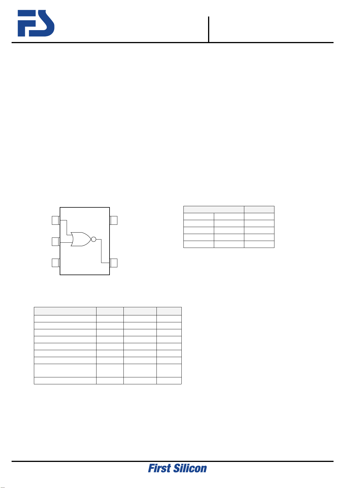
Pin Configuration
◆
1
B
2
A
3
GND
SOT-23-5 (TOP VIEW)
◆
◆◆
Absolute Maximum Ratings
◆
5
V
CC
Y
4
PARAMETER SYMBOL RATINGS UNITS
V
Power Supply Voltage
I
V
V
I
I
I
CC, I
Pd
Tstg
Input voltage
Output Voltage
Input Diode Current
Output Diode current
Output Current
Vcc, GND Current
Continuous Total
Power Dissipation (Ta=55
Storage Temperature
Note: Voltage is all Ground standardized.
°C)
CC
IN
OUT
IK
OK
OUT
GND
-0.5 ~ +6.0
-0.5 ~ +6.0
-0.5 ~ V +0.5
±20
±
20
25
±
50
±
150
-65 ~ +150
◆
◆◆
Function
◆
INPUT OUTPUT
A B Y
L L H
L H H
H L H
H H L
H=High level, L=Low level
°Ta=-40 C~85 °C
V
V
CC
V
mA
mA
mA
mA
mW
°C
V
◆
2007. 8. 30 2/3
FC74UL02
Revision No : 0
◆◆
Recommended Operating Conditions
◆
PARAMETER SYMBOL CONDITIONS UNITS
Supply Voltage
Input Voltage
Output Voltage
Operating Temperature
V
CC
V
IN
V
OUT
Topr
I
OH
Output Current
I
OL
Input Rise and Fall Time tr, tf
◆
◆◆
DC Electrical Characteristics
◆
PARAMETER SYMBOL Vcc(V) CONDITIONS
V (V)
CC
-
-
-
-
3.0
4.5
3.0
4.5
3.3
5.0
2 ~ 5.5
0 ~ 5.5
0 ~ V
CC
-40 ~ +85
-4
-8
4
8
0 ~ 100
0 ~ 20
Ta=25 °°°°C Ta=-40~85 °°°°C
MIN TYP MAX MIN MAX
5.1 0.2 - - 1.5 -
V
Input Voltage
IH
5.5
2.0 - - 0.5 - 0.5
V
IL
3.0 - - 0.9 - 0.9
5.5
1.2 0.3 - - 2.1 -
3.85 - - 3.85 -
- - 1.65 - 1.65
9.1 0.2 2.0 - 1.9 -
.3 3.0 - 2.9 -
OH
V
4.5
3.0 I
Output Voltage
4.5
2.0 - - 0.1 - 0.1
3.0 - - 0.1 - 0.1
OL
V
4.5
3.0 I
4.5
Input Current
I
IN 5.5 V IN=Vcc or GND -0.1 - 0.1 -1.0 1.0
Quiescent Supply Current Icc 5.5 V
OH=-50 µA
IN=VIH or VIL
OH=-4mA 2.58 - - 2.48 -
IOH=-8mA 3.94 - - 3.80 -
I
OL=50 µA
VIN=VIH
OL =4mA - - 0.36 - 0.44
OL =8mA - - 0.36 - 0.44
I
IN=Vcc or GND, I OUT=0µA - - 1.0 - 10.0
9.2 0
4.4 4.5 - 4.4 -
- - 0.1 - 0.1
I
◆
◆◆
Switching Electrical Characteristics
◆
Ta=25 °°°° Ta=-40~85 °°°°C
PARAMETER SYMBOL C
Propagation Delay Time
Input Capacitance
Power Dissipation Capacitance
L Vcc(V) CONDITIONS
15pF
tPLH
50pF
15pF
tPHL
50pF
C
IN
- 5.0 V
Cpd
No Load, f=1MHz pF
3.3
5.0
3.3
5.0
3.3
5.0
3.3
5.0
IN=Vcc or GND
MIN TYP MAX
-
-
-
-
-
-
-
-
-
-
C
7.9 9.5
3.9
5.5 6.5
2.7
11.4 13
5.5
7.5 8.5
3.9
7.9 9.5
3.5
5.5 6.5
2.6
11.4 13
4.9
7.5 8.5
3.6
10
4
9.7
- -
MIN M AX
V
V
V
°C
mA
ns
UNITS
V
V
V
V
µA
µA
Tr=tf=3ns
UNITS
1
1
1
1
1
1
1
1
-
10
ns
ns
ns
ns
pF
-

DISCLAIMER:
2007. 8. 30 3/3
FC74UL02
Revision No : 0
◆
◆◆
Typical Application Circuit
◆
V
CC
Generator
◆
◆◆
Waveforms
◆
Input
Pulse
Z = 50Ω
OUT
10%
Input
Note: Open output when measuring supply current
tr
90%
90%
50%
tf
50%
10%
Output
C
L
V
GND
CC
PRR = 1MHz
duty cycle 50%
tr = tf =3ns
V
OH
Output
50%
t
PHL
t
PLH
50%
V
OL
The information presented in this document does not form part of any quotation or contract, is believed to be accurate and
reliable and may be changed without notice. No liability will be accepted by the publisher for any consequence of its use.
 Loading...