

Page 1

FIBOCOM NL668-AM Hardware
User Manual
Version: V1.0.1
Date: 2018-11-13
FIBOCOM NL668-AM Hardware User Manual Page 1 of 62
Reproduction forbidden without Fibocom Wireless Inc. written authorization - All Rights Reserved.
Page 2
Applicability type
No. Product model Description
1
2
NL668-AM-00
NL668-AM-01
MCP is 4+2, and supports MAIN_ANT, DIV_ANT, GNSS_ANT
Based on NL668-AM-00 delete Band 71
Reproduction forbidden without Fibocom Wireless Inc. written authorization - All Rights Reserved.
FIBOCOM NL668-AM Hardware User Manual Page 2 of 62
Page 3
Copyright
Copyright ©2018 Fibocom Wireless Inc. All rights reserved.
Without the prior written permission of the copyright holder, any company or individual is prohibited to
excerpt, copy any part of or the entire document, or transmit the document in any form.
Attention
The document is subject to update from time to time owing to the product version upgrade or other
reasons. Unless otherwise specified, the document only serves as the user guide. All the statements,
information and suggestions contained in the document do not constitute any explicit or implicit
guarantee.
Trademark
The trademark is registered and owned by Fibocom Wireless Inc.
Versions
Version Author Assessor Approver
V1.0.0
V1.0.1
Gaoying Chenguojiang Tumin
Gaoying Chenguojiang Tumin
Update
Date
2018-10-26 Initial version
2018-11-13 Add Band 17
Description
Reproduction forbidden without Fibocom Wireless Inc. written authorization - All Rights Reserved.
FIBOCOM NL668-AM Hardware User Manual Page 3 of 62
Page 4

Contents
1 Foreword ....................................................................................................................... 9
1.1
1.2
1.3
1.4
1.5 Federal Communication Commission Interference Statement..................................... 11
Introduction ................................................................................................................... 9
Safety Instruction .......................................................................................................... 9
Reference Standards .................................................................................................. 10
Related Document ...................................................................................................... 11
2 Product Overview ....................................................................................................... 13
2.1
2.2
2.3
Product Introduction ................................................................................................... 13
Product Specifications ................................................................................................ 13
Hardware Diagram ..................................................................................................... 14
3 Application Interface .................................................................................................. 16
3.1
LCC Interface ............................................................................................................. 16
3.1.1 Pin distribution ............................................................................................................... 16
3.1.2 Pin definition .................................................................................................................. 17
3.2 Power Supply ............................................................................................................. 22
3.2.1 Power supply ................................................................................................................. 23
3.2.2 1.8V Output ................................................................................................................... 24
3.2.3 Power consumption....................................................................................................... 24
3.3
3.4
3.5
Control Signal ............................................................................................................. 25
3.3.1 Module power on ........................................................................................................... 26
3.3.2 Module power off ........................................................................................................... 27
3.3.3 Module reset ................................................................................................................. 28
USB Interface ............................................................................................................. 30
3.4.1 USB interface definition ................................................................................................ 30
USIM Interface ........................................................................................................... 31
3.5.1 USIM pin ........................................................................................................................ 31
3.5.2 USIM interface circuit .................................................................................................... 31
3.5.3 USIM hot plug ............................................................................................................... 33
3.5.4 USIM design requirements ........................................................................................... 34
3.6
3.7
FIBOCOM NL668-AM Hardware User Manual Page 4 of 62
UART Interface ........................................................................................................... 34
3.6.1 UART interface definition .............................................................................................. 34
3.6.2 UART port application ................................................................................................... 35
Status Indicator ........................................................................................................... 36
Reproduction forbidden without Fibocom Wireless Inc. written authorization - All Rights Reserved.
Page 5

3.7.1 NET_MODE Signal ....................................................................................................... 36
3.8
3.9
Low Power Mode ........................................................................................................ 37
3.8.1 Flight mode.................................................................................................................... 37
3.8.2 Sleep Mode ................................................................................................................... 38
Digital audio interface PCM ........................................................................................ 40
3.9.1 Support model ............................................................................................................... 40
3.9.2 PCM interface definition ................................................................................................ 40
3.9.3 PCM interface description ............................................................................................. 40
3.9.4 PCM signal description ................................................................................................. 41
3.10 ADC function .............................................................................................................. 42
4 RF Interface................................................................................................................. 43
4.1
4.2 RF Output Power of NL668-AM .................................................................................. 43
4.3
4.4
NL668-AM Operating Frequency ................................................................................ 43
RF Receiving Sensitivity of NL668-AM ....................................................................... 44
GNSS Receiver .......................................................................................................... 44
4.4.1 Basic description ........................................................................................................... 44
4.5
4.6
RF PCB Design .......................................................................................................... 45
4.5.1 Antenna RF connector .................................................................................................. 45
Antenna Design .......................................................................................................... 46
5 Electrical Characteristics .......................................................................................... 49
5.1
5.2
5.3
5.4
5.5
Limiting voltage range................................................................................................. 49
Environment temperature range ................................................................................. 49
Electrical characteristics of the interface in operating status ....................................... 49
Environmental reliability requirements ........................................................................ 50
ESD characteristics .................................................................................................... 51
6 Structure Specification .............................................................................................. 52
6.1
6.2
6.3
Product Appearance ................................................................................................... 52
Dimension of Structure ............................................................................................... 53
SMT Patch .................................................................................................................. 53
Appendix A Terms and Acronyms ................................................................................... 54
Appendix B ADP & MiniPCIe RF ports trace………………………………………………... 57
Reproduction forbidden without Fibocom Wireless Inc. written authorization - All Rights Reserved.
FIBOCOM NL668-AM Hardware User Manual Page 5 of 62
Page 6

Figure
Figure 2-1 Hardware Diagram ............................................................................................................ 15
Figure 3-1 Pin Distribution Diagram(TOP plan perspective diagram) ................................................ 16
Figure 3-2 Power Design .................................................................................................................... 23
Figure 3-3 Power Limit ........................................................................................................................ 24
Figure 3-4 OC/OD Drive Power on Reference Circuit ........................................................................ 26
Figure 3-5 Button Power on Reference Circuit ................................................................................... 26
Figure 3-6 Power on Timing Control Diagram .................................................................................... 27
Figure 3-7 Power off Timing Control Diagram .................................................................................... 28
Figure 3-8 RESET_N OC/OD Drive Reference Circuit ...................................................................... 29
Figure 3-9 RESET_N Button Reference Circuit ................................................................................. 29
Figure 3-10 Reset Control Timing ....................................................................................................... 29
Figure 3-11 SIM Card Slot Diagram SIM016-8P-220P ....................................................................... 32
Figure 3-12 USIM/SIM Interface with Detection Signal Reference Design ........................................ 32
Figure 3-13 USIM/SIM Interface without Detection Signal Reference Design Diagram .................... 33
Figure 3-14 UART Level Translate Reference Circuit 1 ..................................................................... 35
Figure 3-15 UART Level Translate Reference Circuit 2 ..................................................................... 36
Figure 3-16 NET_MODE Reference Design Diagram........................................................................ 37
Figure 3-17 PCM_SYNC Timing ......................................................................................................... 41
Figure 3-18 PCM_CODEC to NL668-AM Timing ............................................................................... 41
Figure 3-19 NL668-AM to PCM_CODEC Timing ............................................................................... 41
Figure 3-20 CODEC Timing Parameters ............................................................................................ 42
Figure 4-1RF Reference Circuit Design ............................................................................................. 45
Figure 4-2 GNSS RF Reference Circuit ............................................................................................. 46
Figure 6-1Module Product Appearance (Top) .................................................................................... 52
Figure 6-2 Module Product Appearance (Bottom) .............................................................................. 52
Figure 6-3 Dimension of Structure (Unit: mm) .................................................................................... 53
Reproduction forbidden without Fibocom Wireless Inc. written authorization - All Rights Reserved.
FIBOCOM NL668-AM Hardware User Manual Page 6 of 62
Page 7

Table
Table 2-1 Product Specifications......................................................................................................... 14
Table 3-1 Pin Definitions ..................................................................................................................... 22
Table 3-2 Power Interfaces ................................................................................................................. 22
Table 3-3 Power Filter Capacitor Design ............................................................................................ 23
Table 3-4 VDD_EXT Logic Level ........................................................................................................ 24
Table 3-5 Power Consumption ............................................................................................................ 25
Table 3-6 Control Signal...................................................................................................................... 26
Table 3-7 Power Off Modes ................................................................................................................ 27
Table 3-8 Module Reset ...................................................................................................................... 28
Table 3-9 USB Interface Definition ..................................................................................................... 30
Table 3-10 SIM Card Pin ..................................................................................................................... 31
Table 3-11SIM Card Hot Plug Function Configured AT Commands ................................................... 33
Table 3-12 USIM_PRESENCE Effective Level Switched AT command ............................................. 34
Table 3-13 Main Serial Port Pin .......................................................................................................... 35
Table 3-14 Debug Serial Port Pin ....................................................................................................... 35
Table 3-15 Network Indication pins ..................................................................................................... 36
Table 3-16 Network Indicator Status Description ................................................................................ 37
Table 3-17 W_DISABLE# Pin Description .......................................................................................... 37
Table 3-18 Module enter Fly Mode ..................................................................................................... 37
Table 3-19 Support model ................................................................................................................... 40
Table 3-20 PCM Interface Definition ................................................................................................... 40
Table 3-21 PCM Interface Description ................................................................................................ 40
Table 3-22 ADC Interface .................................................................................................................... 42
Table 4-1Operating Frequency ........................................................................................................... 43
Table 4-2 RF Output Power ................................................................................................................ 43
Table 4-3 RF Receiving Sensitivity ..................................................................................................... 44
Table 4-4 GNSS Receiver ................................................................................................................... 45
Table 4-5 Main Antenna Requirement ................................................................................................ 48
Table 5-1 Voltage Range ..................................................................................................................... 49
Table 5-2Environment Temperature Range ........................................................................................ 49
Table 5-3 Electrical Characteristics of the Interface in Operating Status ........................................... 50
Table 5-4 Environmental Reliability Requirements ............................................................................. 50
Table 5-5 ESD Allowable Discharge Range ....................................................................................... 51
Reproduction forbidden without Fibocom Wireless Inc. written authorization - All Rights Reserved.
FIBOCOM NL668-AM Hardware User Manual Page 7 of 62
Page 8

Table A-0-1 Terms and Acronyms ....................................................................................................... 56
Reproduction forbidden without Fibocom Wireless Inc. written authorization - All Rights Reserved.
FIBOCOM NL668-AM Hardware User Manual Page 8 of 62
Page 9
1 Foreword
1.1 Introduction
This document describes the electrical characteristics, RF performance, structure size, application
environment, etc. of NL668-AM module. With the assistance of the document and other instructions, the
developers can quickly understand the hardware functions of the NL668-AM module and develop
products.
1.2 Safety Instruction
By following the safety guidelines below, you can ensure your personal safety and help protect the
product and work environment from potential damage. Product manufacturers need to communicate the
following safety instructions to end users. In case of failure to comply with these safety rules, Fibocom will
not be responsible for the consequences caused by the user’s misuse.
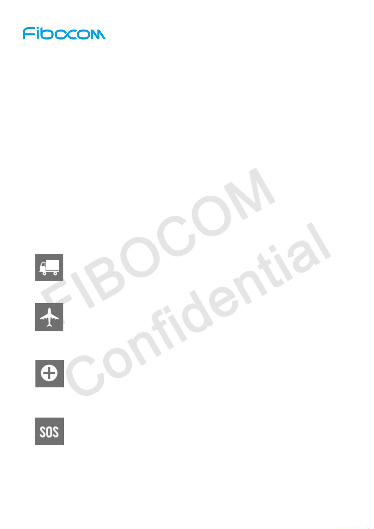
Road safety first! When you drive, do not use the handheld devices even if it has a
hand-free feature. Please stop and call.
Please turn off the mobile device before boarding. The wireless feature of the mobile
device is not allowed on the aircraft to prevent interference with the aircraft communication
system. Ignoring this note may result in flight safety issue or even breaking the law.
When in a hospital or health care facility, please be aware of restrictions on the use
of mobile devices. Radio frequency interference may cause medical equipment to
malfunction, so it may be necessary to turn off the mobile device.
The mobile device does not guarantee that an effective connection can be made under
any circumstances, for example, when there is no prepayment for the mobile device or the
SIM is invalid. When you encounter the above situation in an emergency, remember to use
an emergency call, while keeping your device turned on and in areas where signal is
strong.
Reproduction forbidden without Fibocom Wireless Inc. written authorization - All Rights Reserved.
FIBOCOM NL668-AM Hardware User Manual Page 9 of 62
Page 10

Your mobile device receives and transmits RF signals when it is powered on. Radio
interference occurs when it is near televisions, radios, computers, or other electronic
devices.
Keep the mobile device away from flammable gases. Turn off the mobile device when
near gas stations, oil depots, chemical plants or explosive workplaces. There is a safety
hazard in operating electronic equipment in any potentially explosive environment.
1.3 Reference Standards
This design of the product complies with the following standards:
3GPP TS 51.010-1 V10.5.0: Mobile Station (MS) conformance specification; Part 1:
Conformance specification
3GPP TS 34.121-1 V10.8.0: User Equipment (UE) conformance specification; Radio
transmission and reception (FDD); Part 1: Conformance specification
3GPP TS 34.122 V10.1.0: Technical Specification Group Radio Access Network; Radio
transmission and reception (TDD)
3GPP TS 36.521-1 V10.6.0: User Equipment (UE) conformance specification; Radio
transmission and reception; Part 1: Conformance testing
3GPP TS 21.111 V10.0.0: USIM and IC card requirements
3GPP TS 51.011 V4.15.0: Specification of the Subscriber Identity Module -Mobile Equipment
(SIM-ME) interface
3GPP TS 31.102 V10.11.0: Characteristics of the Universal Subscriber Identity Module (USIM)
application
3GPP TS 31.11 V10.16.0: Universal Subscriber Identity Module (USIM) Application
Toolkit(USAT)
3GPP TS 36.124 V10.3.0: Electro Magnetic Compatibility (EMC) requirements for mobile
terminals and ancillary equipment
3GPP TS 27.007 V10.0.8: AT command set for User Equipment (UE)
3GPP TS 27.005 V10.0.1: Use of Data Terminal Equipment - Data Circuit terminating Equipment
(DTE - DCE) interface for Short Message Service (SMS) and Cell Broadcast Service (CBS)
Reproduction forbidden without Fibocom Wireless Inc. written authorization - All Rights Reserved.
FIBOCOM NL668-AM Hardware User Manual Page 10 of 62
Page 11

1.4 Related Document
FIBOCOM_RF Antenna Application Design Instruction
FIBOCOM_ADP-NL668 Evaluation board instruction
FIBOCOM_NL668 AT Command Manual
FIBOCOM_EVK-GT8230-NL User Manual
FIBOCOM_ NL668 LCC SMT Application Design Instruction
1.5 Federal Communication Commission Interference
Statement
FCC Regulations:
This device complies with part 15 of the FCC Rules. Operation is subject to the following two conditions:
(1) This device may not cause harmful interference, and (2) This device must accept any interference
received, including interference that may cause undesired operation.
This device has been tested and found to comply with the limits for a Class B digital device , pursuant to
Part 15 of the FCC Rules. These limits are designed to provide reasonable protection against harmful
interference in a residential installation. This equipment generates, uses and can radiated radio frequency
energy and, if not installed and used in accordance with the instructions, may cause harmful interference
to radio communications. However, there is no guarantee that interference will not occur in a particular
installation If this equipment does cause harmful interference to radio or television reception, which can
be determined by turning the equipment off and on, the user is encouraged to try to correct the
interference by one or more of the following measures:
-Reorient or relocate the receiving antenna.
-Increase the separation between the equipment and receiver.
-Connect the equipment into an outlet on a circuit different from that to which the receiver is connected.
-Consult the dealer or an experienced radio/TV technician for help.
Caution: Changes or modifications not expressly approved by the party responsible for compliance could
void the user‘s authority to operate the equipment.
RF Exposure Information:
This device complies with FCC radiation exposure limits set forth for an uncontrolled environment. In
order to avoid the possibility of exceeding the FCC radio frequency exposure limits, human proximity to
the antenna shall not be less than 20cm (8 inches) during normal operation.
Reproduction forbidden without Fibocom Wireless Inc. written authorization - All Rights Reserved.
FIBOCOM NL668-AM Hardware User Manual Page 11 of 62
Page 12
IMPORTANT NOTE :
This module is intended for OEM integrator. The OEM integrator is still responsible for the FCC
compliance requirement of the end product, which integrates this module. 20cm minimum distance has to
be able to be maintained between the antenna and the users for the host this module is integrated into.
Under such configuration, the FCC radiation exposure limits set forth for an population/uncontrolled
environment can be satisfied.
Any changes or modifications not expressly approved by the manufacturer could void the user's authority
to operate this equipment.
USERS MANUAL OF THE END PRODUCT :
In the user manual of the end product, the end user has to be informed to keep at least 20cm separation
with the antenna while this end product is installed and operated. The end user has to be informed that
the FCC radio-frequency exposure guidelines for an uncontrolled environment can be satisfied. The end
user has to also be informed that any changes or modifications not expressly approved by the
manufacturer could void the user's authority to operate this equipment. If the size of the end product is
smaller than 8x10cm, then additional FCC part 15.19 statement is required to be available in the users
manual: This device complies with Part 15 of FCC rules. Operation is subject to the following two
conditions: (1) this device may not cause harmful interference and (2) this device must accept any
interference received, including interference that may cause undesired operation.
LABEL OF THE END PRODUCT :
The final end product must be labeled in a visible area with the following " Contains Transmitter Module
FCC ID: ZMONL668AM01". If the size of the end product is larger than 8x10cm, then the following FCC
part 15.19 statement has to also be available on the label: This device complies with Part 15 of FCC rules.
Operation is subject to the following two conditions: (1) this device may not cause harmful interference
and (2) this device must accept any interference received, including interference that may cause
undesired operation.
Reproduction forbidden without Fibocom Wireless Inc. written authorization - All Rights Reserved.
FIBOCOM NL668-AM Hardware User Manual Page 12 of 62
Page 13
2 Product Overview
2.1 Product Introduction
The NL668-AM wireless module is a wideband wireless terminal product applicable to various network
formats and multi-bands including FDD-LTE/UMTS.
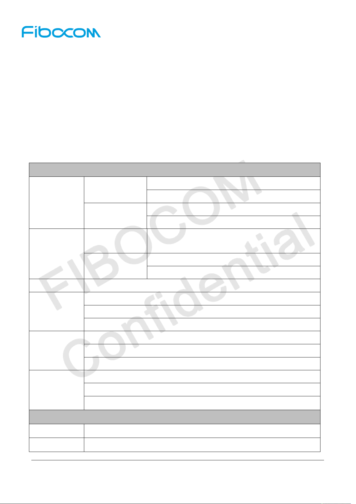
2.2 Product Specifications
Specification
LTE FDD: Band 2,4,5,12,13,17,66,71
NL668-AM-00
Operating
WCDMA: Band 2,4,5
frequency
Data
transmission
Power
Temperature
Power
consumption
Physical
characteristics
LTE FDD: Band 2,4,5,12,13,17,66
NL668-AM-01
WCDMA: Band 2,4,5
150Mbps DL/50Mbps UL(Cat 4); LTE Downlink MIMO 2x2,
LTE FDD Rel.9
4x2
WCDMA:384 kbps DL/384 kbps UL
WCDMA Rel.8
DC-HSDPA+:42Mbps (Cat 24)/HSUPA:5.76Mbps (Cat 6)
3.3V~4.3V (3.8V recommended)
Normal: -30°C~+75°C
Extended: -40°C~+85°C
Storage: -40°C~+85°C
Base current: <1.5mA
Sleep mode: ≤3mA
Idle mode: <20mA
Package: LCC 144PIN
Size: 32.0×29.0×2.4 mm
Weight: About 5.5g
Interface
Antenna
Functional
Reproduction forbidden without Fibocom Wireless Inc. written authorization - All Rights Reserved.
FIBOCOM NL668-AM Hardware User Manual Page 13 of 62
Antenna: Main x 1, GNSS x 1, DIV x 1
USIM 3.0V/1.8V
Page 14
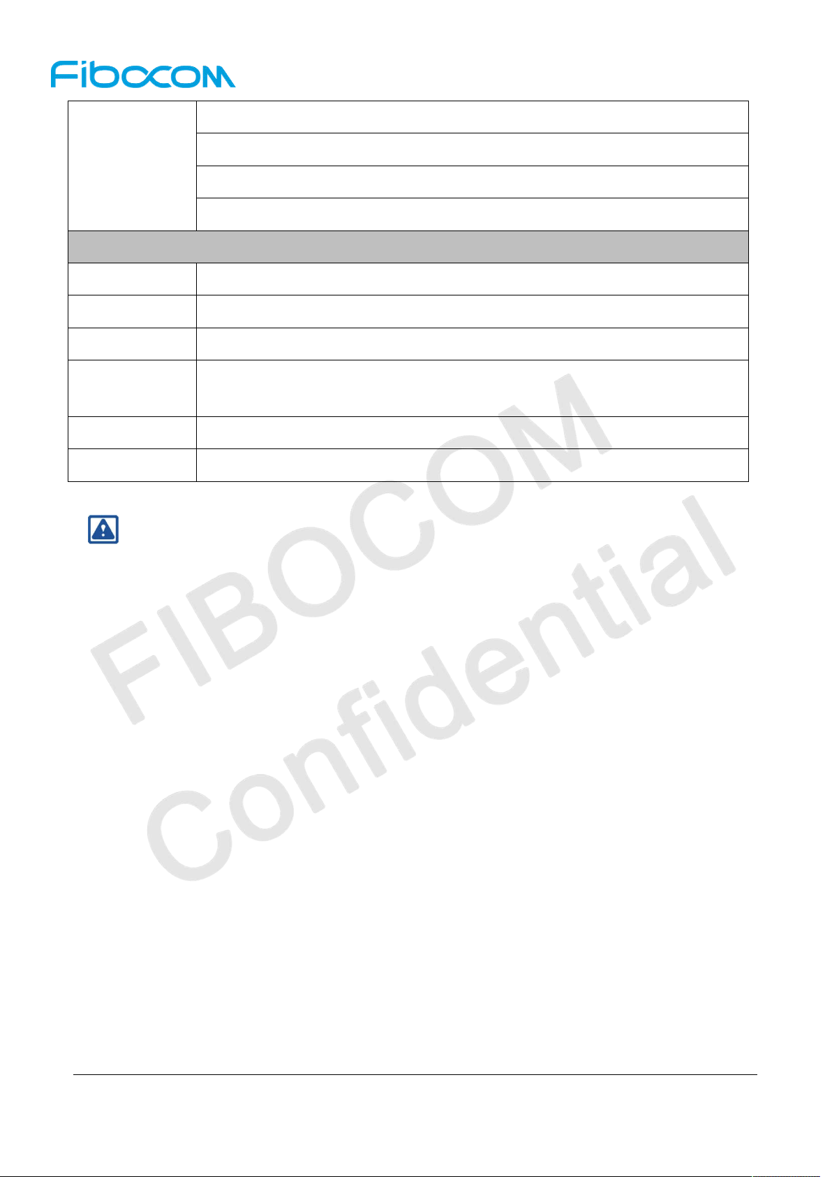
Interface
Software
Protocol Stack
AT Command 3GPP TS 27.007 and 27.005, and proprietary FIBOCOM AT
Firmware update USB(UART does not support DOWNLOAD)
Voice service
SMS
MMS service
Note:
USB 2.0 x 1
UART, PCM, I2C, SGMII, SDIO, GPIO, SPI
System Indicator
ADC
Embedded TCP/IP and UDP/IP protocol stack
VoLTE, HR, FR, EFR, AMR, DTMF, Caller ID, Call Transfer, Call Hold, Call Waiting
and Multi-Talk, etc.
point-to-point MO, MT; cell broadcast; support Text and PDU modes
Need AP to realize MMS protocol
Table 2-1 Product Specifications
When the temperature is beyond the normal operating temperature range (-30 °C to + 75 °C),
the RF performance of the module may slightly exceed the 3GPP specifications.
2.3 Hardware Diagram
Figure 2-2 hardware diagram shows the main hardware features of the NL668-AM module, including
baseband and RF features.
Baseband includes:
UMTS/ LTE FDD controller
PMIC
MCP
UART、USB、SIM、PCM、I2C、SPI、SGMII、SDIO、ADC
RF includes:
RF Transceiver
RF PA
RF filter
Antenna
Reproduction forbidden without Fibocom Wireless Inc. written authorization - All Rights Reserved.
FIBOCOM NL668-AM Hardware User Manual Page 14 of 62
Page 15
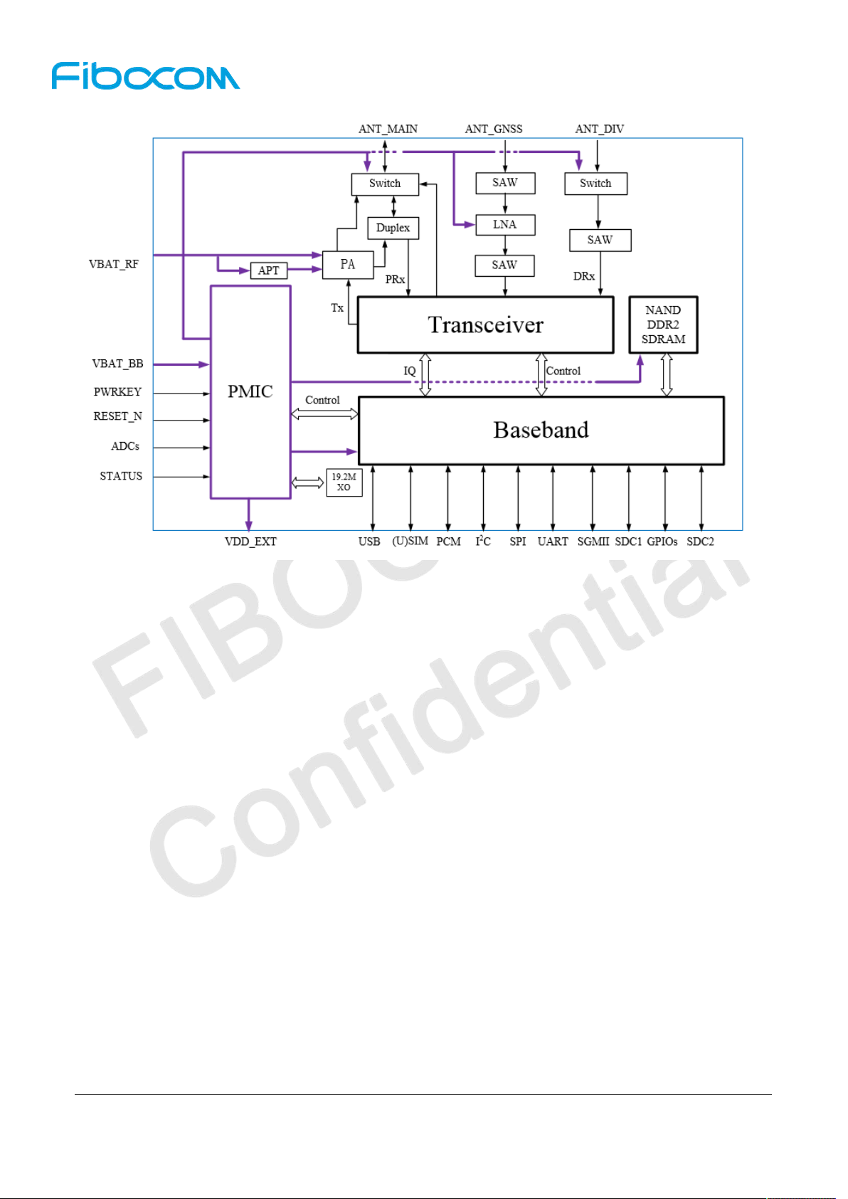
Figure 2-1 Hardware Diagram
Reproduction forbidden without Fibocom Wireless Inc. written authorization - All Rights Reserved.
FIBOCOM NL668-AM Hardware User Manual Page 15 of 62
Page 16
3 Application Interface
3.1 LCC Interface
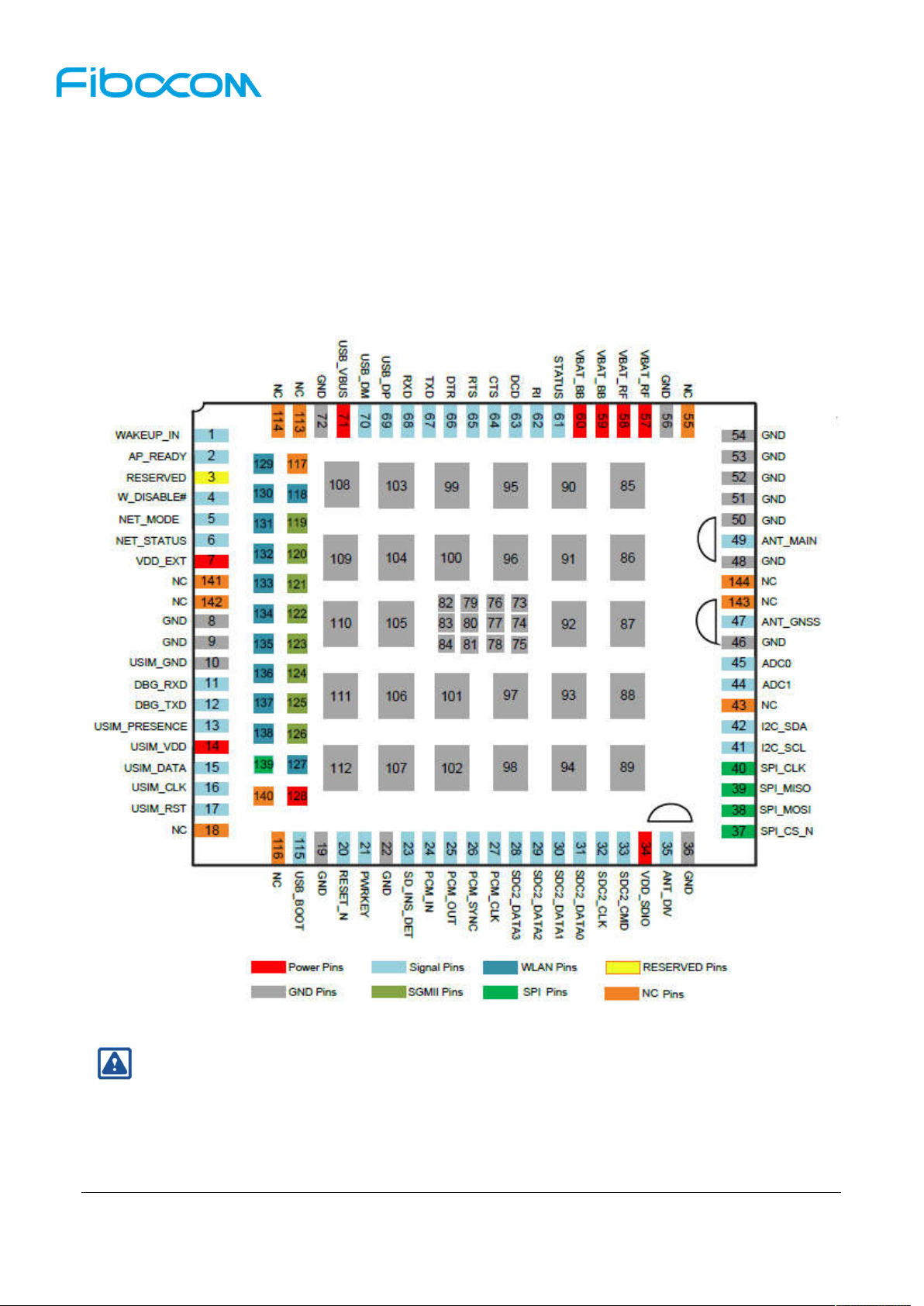
NL668-AM module adopts LCC packaging, with a total of 144 pins.
3.1.1 Pin distribution
Figure 3-1 Pin Distribution Diagram(TOP plan perspective diagram)
Note:
“73 ~ 112” is the thermal pin, and the module is grounded internally. It is recommended that the
heat sink pad is reserved for PCB packaging and welded.
Reproduction forbidden without Fibocom Wireless Inc. written authorization - All Rights Reserved.
FIBOCOM NL668-AM Hardware User Manual Page 16 of 62
Page 17
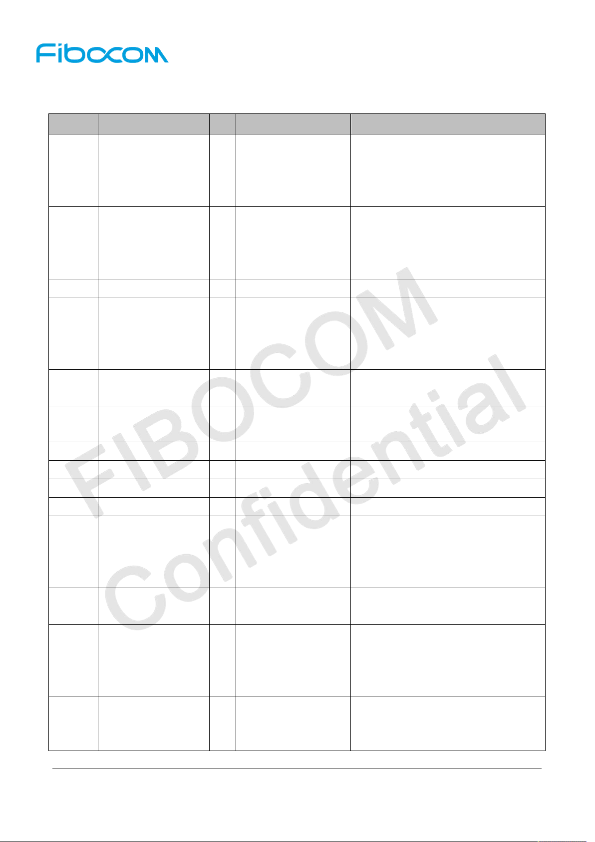
3.1.2 Pin definition
The pin definitions are shown in the following table:
Pin Pin Name I/O Level Description
VILmin=-0.3V
1 WAKEUP_IN I
External device wake-up module
VIHmin=1.2V
VIHmax=2.0V
VILmin=-0.3V
VILmax=0.6V
VILmax=0.6V
2 AP_READY I
Reserved
VIHmin=1.2V
VIHmax=2.0V
3 RESERVED - Reserved
VILmin=-0.3V
VILmax=0.6V
4 W_DISABLE# I
Module flight mode control
VIHmin=1.2V
VIHmax=2.0V
VOHmin=1.35V
5 NET_MODE O
Module state indicate
VOLmax=0.45V
VOHmin=1.35V
6 NET_STATUS O
Reserved
VOLmax=0.45V
7 VDD_EXT PO 1.8V Module digital level, 1.8V output, 80mA
8 GND G - Ground
9 GND G - Ground
10 GND G - Ground
VILmin=-0.3V
VILmax=0.6V
11 DBG_RXD I
DEBUG serial port Receive data
VIHmin=1.2V
VIHmax=2.0V
VOLmax=0.45V
12 DBG_TXD O
DEBUG serial port Transmit data
VOHmin=1.35V
VILmin=-0.3V
VILmax=0.6V
13 USIM_PRESENCE I
USIM card hot plug detection
VIHmin=1.2V
VIHmax=2.0V
For 1.8V USIM:
14 USIM _VDD O
Vmax=1.9V
USIM power
Vmin=1.7V
Reproduction forbidden without Fibocom Wireless Inc. written authorization - All Rights Reserved.
FIBOCOM NL668-AM Hardware User Manual Page 17 of 62
Page 18
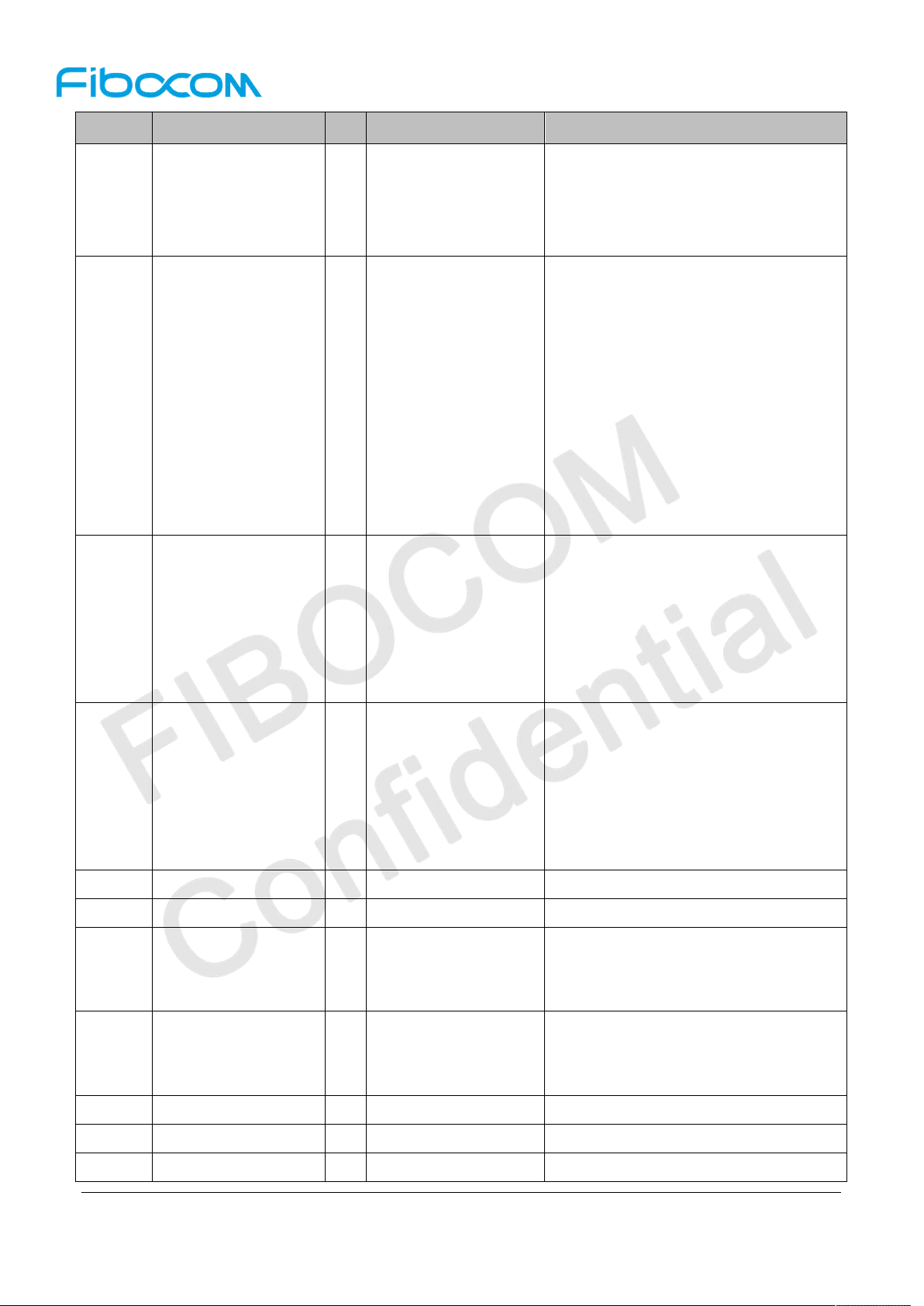
Pin Pin Name I/O Level Description
For 3.0V USIM:
Vmax=3.05V
Vmin=2.7V
IOmax=150mA
For 1.8V USIM:
VILmax=0.6V
VIHmin=1.2V
VOLmax=0.45V
15 USIM _DATA O
16 USIM _CLK O
17 USIM _RST O
VOHmin=1.35V
USIM data signal cable
For 3.0V USIM:
VILmax=1.0V
VIHmin=1.95V
VOLmax=0.45V
VOHmin=2.55V
For 1.8V USIM:
VOLmax=0.45V
VOHmin=1.35V
USIM clock signal cable
For3.0V USIM:
VOLmax=0.45V
VOHmin=2.55V
For 1.8V USIM:
VOLmax=0.45V
VOHmin=1.35V
USIM reset signal cable
For 3.0V USIM:
VOLmax=0.45V
VOHmin=2.55V
18 NC - - NC
19 GND G - Ground
VIHmax=2.1V
Module reset signal, active low, no
20 RESET_N I
VIHmin=1.3V
need pull up externally
VILmax=0.5V
VIHmax=2.1V
Turn on/off the module, active low, no
21 PWRKEY I
VIHmin=1.3V
need pull up externally
VILmax=0.5V
22 GND G - Ground
23 SD_INS_DET I - Reserved
24 PCM_IN I VILmin=-0.3V PCM input signal
Reproduction forbidden without Fibocom Wireless Inc. written authorization - All Rights Reserved.
FIBOCOM NL668-AM Hardware User Manual Page 18 of 62
Page 19
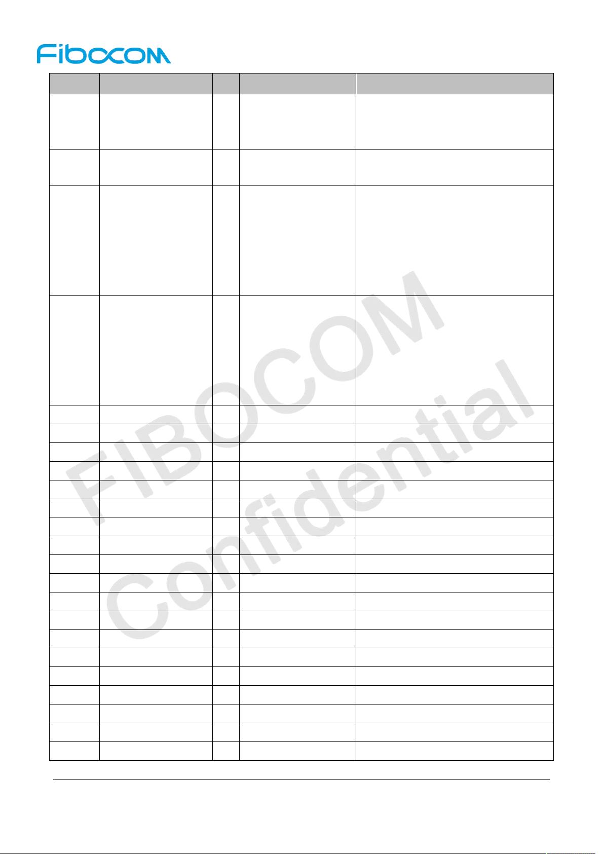
Pin Pin Name I/O Level Description
VILmax=0.6V
VIHmin=1.2V
VIHmax=2.0V
25 PCM_OUT O
PCM output signal
VOHmin=1.35V
VOLmax=0.45V
VOHmin=1.35V
VILmin=-0.3V
VOLmax=0.45V
26 PCM_SYNC I/O
PCM synchronization signal
VILmax=0.6V
VIHmin=1.2V
VIHmax=2.0V
VOLmax=0.45V
VOHmin=1.35V
VILmin=-0.3V
27 PCM_CLK I/O
PCM clock signal
VILmax=0.6V
VIHmin=1.2V
VIHmax=2.0V
28 SDC2_DATA3 I/O - Reserved
29 SDC2_DATA2 I/O - Reserved
30 SDC2_DATA1 I/O - Reserved
31 SDC2_DATA0 I/O - Reserved
32 SDC2_CLK O - Reserved
33 SDC2_CMD I/O - Reserved
34 VDD_SDIO PO - Reserved
35 ANT_DIV I - Diversity antenna
36 GND G - Ground
37 SPI_CS_N I - Reserved
38 SPI_MOSI I - Reserved
39 SPI_MISO O - Reserved
40 SPI_CLK O - Reserved
41 I2C_SCL OD - I2C interface clock signal
42 I2C_SDA OD - I2C interface data signal
43 NC - - NC
44 ADC1 I - Analog to digital converter interface
45 ADC0 I - Analog to digital converter interface 0
46 GND G - Ground
Reproduction forbidden without Fibocom Wireless Inc. written authorization - All Rights Reserved.
FIBOCOM NL668-AM Hardware User Manual Page 19 of 62
Page 20
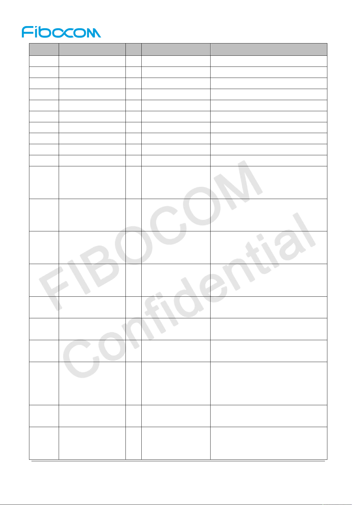
Pin Pin Name I/O Level Description
47 ANT_GNSS I - GNSS antenna
48 GND G - Ground
49 ANT_MAIN I/O - Main antenna
50 GND G - Ground
51 GND G - Ground
52 GND G - Ground
53 GND G - Ground
54 GND G - Ground
55 NC - - NC
56 GND G - Ground
Vmax=4.3V
57 VBAT_RF I
58 VBAT_RF I
59 VBAT_BB I
60 VBAT_BB I
61 STATUS O
62 RI O
63 DCD O
Vmin=3.3V
Vnorm=3.8V
Vmax=4.3V
Vmin=3.3V
Vnorm=3.8V
Vmax=4.3V
Vmin=3.3V
Vnorm=3.8V
Vmax=4.3V
Vmin=3.3V
Vnorm=3.8V
VOHmin=1.35V
VOLmax=0.45V
VOLmax=0.45V
VOHmin=1.35V
VOLmax=0.45V
VOHmin=1.35V
RF power input (3.3V~4.3V)
RF power input (3.3V~4.3V)
Baseband power input(3.3V~4.3V)
Baseband Power Input (3.3V~4.3V)
Reserved
Module output ring indicator
Module output data carrier detection
VILmin=-0.3V
VILmax=0.6V
64 CTS I
Clear to send
VIHmin=1.2V
VIHmax=2.0V
VOLmax=0.45V
65 RTS O
Request to send
VOHmin=1.35V
VILmin=-0.3V
66 DTR I
VILmax=0.6V
Data ready
VIHmin=1.2V
Reproduction forbidden without Fibocom Wireless Inc. written authorization - All Rights Reserved.
FIBOCOM NL668-AM Hardware User Manual Page 20 of 62
Page 21
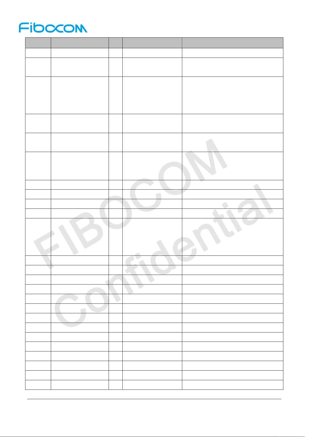
Pin Pin Name I/O Level Description
VIHmax=2.0V
67 TXD O
Transmit data
VOHmin=1.35V
VILmin=-0.3V
VILmax=0.6V
VOLmax=0.45V
68 RXD I
Receive data
VIHmin=1.2V
VIHmax=2.0V
Conform to USB2.0
69 USB_DP I/O
USB differential data bus (+)
standard specification
Conform to USB2.0
70 USB_DM I/O
USB differential data bus (-)
standard specification
Vmax=5.25V
71 USB_VBUS I
Vmin=3.0V
USB plug detection
Vnorm=5.0V
72 GND G - Ground
73-112 GND G - Ground
113 NC - - NC
114 NC - - NC
VILmin=-0.3V
Emergency download
VILmax=0.6V
115 USB_BOOT I
high level active
VIHmin=1.2V
recommended to reserve test point
VIHmax=2.0V
116 NC - - NC
117 NC - - NC
118 WLAN&SDIO I/O Reserved
119 EPHY_RST_N O Reserved
120 EPHY_INT_N I Reserved
121 SGMII_MDATA I/O Reserved
122 SGMII_MCLK O Reserved
123 SGMII_TX_M O Reserved
124 SGMII_TX_P O Reserved
125 SGMII_RX_P I Reserved
126 SGMII_RX_M I Reserved
127 PM_ENABLE I Reserved
128 VREG_L5_UIM2 PO Reserved
129 SDC1_DATA_3 I/O Reserved
Reproduction forbidden without Fibocom Wireless Inc. written authorization - All Rights Reserved.
FIBOCOM NL668-AM Hardware User Manual Page 21 of 62
Page 22
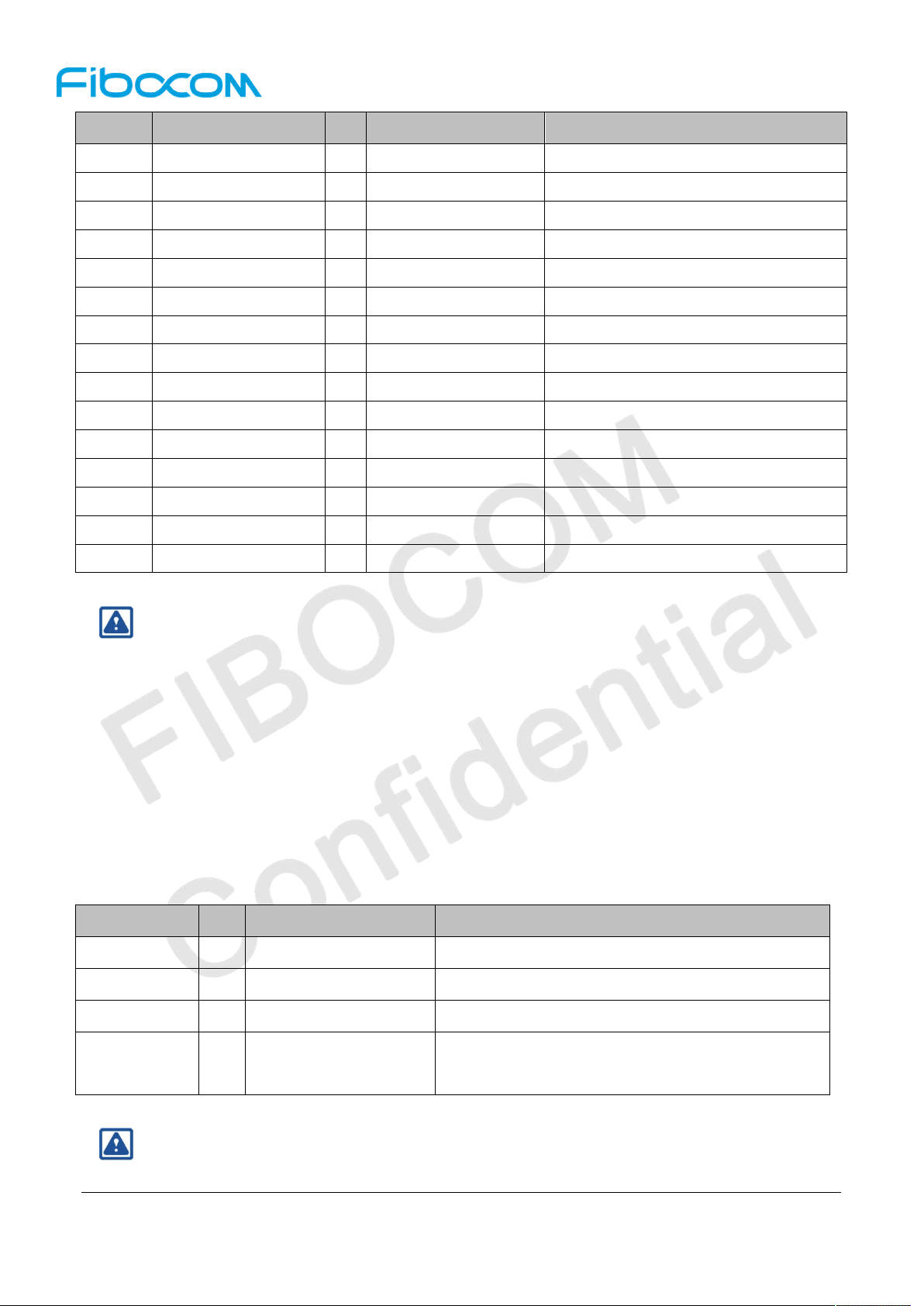
Pin Pin Name I/O Level Description
130 SDC1_DATA_2 I/O Reserved
131 SDC1_DATA_1 I/O Reserved
132 SDC1_DATA_0 I/O Reserved
133 SDC1_CLK O Reserved
134 SDC1_CMD I/O Reserved
135 WAKE_WLAN I Reserved
136 WLAN_EN I Reserved
137 COEX_UART_RXD I Reserved
138 COEX_UART_TXD I/O Reserved
139 BT_EN I Reserved
140 NC - - NC
141 NC - - NC
142 NC - - NC
143 NC - - NC
144 NC - - NC
Table 3-1 Pin Definitions
Note:
Keep the unused pins floating.
Pin73~Pin112 is the module thermal pad, and the corresponding ground pad is reserved for PCB
packaging and welded.
3.2 Power Supply
The power interfaces of NL668-AM module are shown in the following table:
Pin Name I/O Pin Description
VBAT_RF I 57,58 Module power supply, 3.3~4.3V, typical value 3.8V
VBAT_BB I 59,60 Module power supply, 3.3~4.3V, typical value 3.8V
VDD_EXT O 7 Voltage Output, 1.8V, 80mA
GND -
Note:
In the rest of the document, VBAT_BB, VBAT_RF will be replaced with VBAT.
Reproduction forbidden without Fibocom Wireless Inc. written authorization - All Rights Reserved.
FIBOCOM NL668-AM Hardware User Manual Page 22 of 62
8,9,10,19,22,36,46,48,5
Ground
0-54,56,72-112
Table 3-2 Power Interfaces
Page 23
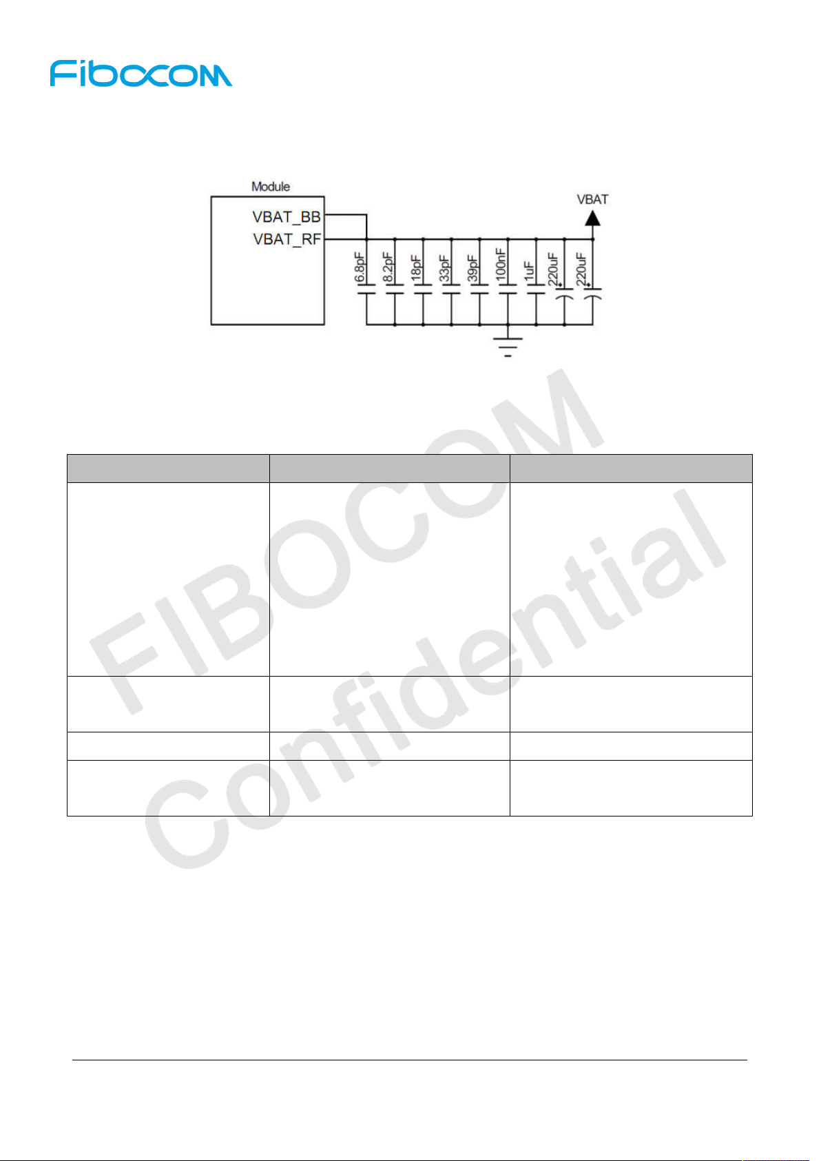
3.2.1 Power supply
The NL668-AM module needs to be powered by the VBAT pin. The power design is shown in Figure 3-2:
Figure 3-2 Power Design
Power filter capacitor design is shown in the following table:
Recommended capacitor Application Description
Reduce power fluctuations during
module operation, requiring low
ESR Capacitor
220uF x 2 Regulating capacitor
LDO or DCDC power requires
not less than 440uF capacitor
Battery power can be properly
reduced to 100 ~ 220uF capacitor
Filter clock and digital signal
1uF,100nF Digital signal noise
interference
39pF,33pF 700, 850/900 MHz bands Filter low band RF interference
1700/1800/1900,2100/2300,2500/2
Filter middle/high band RF
18pF,8.2pF,6.8pF
600MHz bands
Table 3-3 Power Filter Capacitor Design
interference
The power stability ensures the normal operation of NL668-AM module. The design requires special
attention to the power ripple below 300mV(The circuit ESR < 100mΩ). When the module is operating in
WCDMA/LTE mode (Burst transmit), the maximum operating current can reach 2A, and the power voltage
needs to be at least 3.3V. Otherwise, the module may power off or restart. The power limit is shown in
Figure 3-3:
Reproduction forbidden without Fibocom Wireless Inc. written authorization - All Rights Reserved.
FIBOCOM NL668-AM Hardware User Manual Page 23 of 62
Page 24
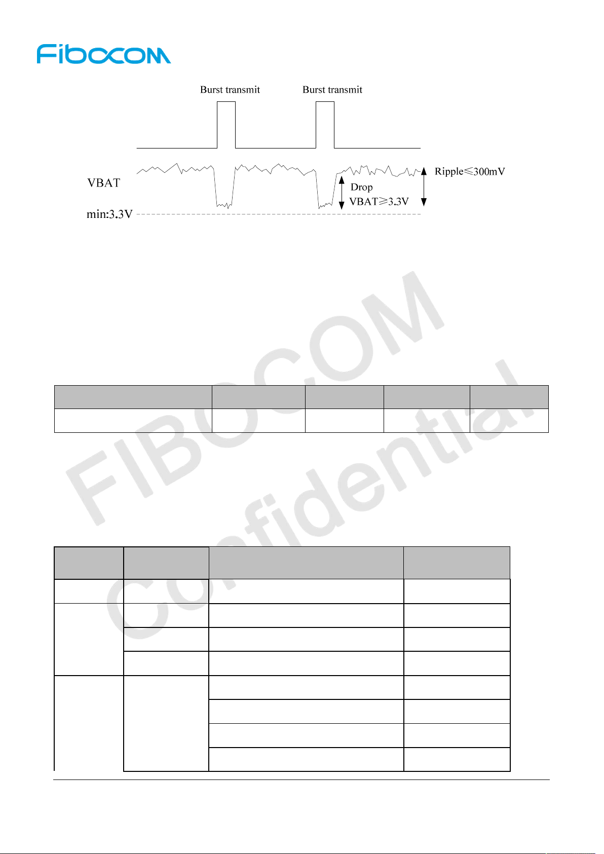
Figure 3-3 Power Limit
3.2.2 1.8V Output
The NL668-AM outputs a 1.8V voltage through the VDD_EXT for use of the internal digital circuit of the
module. The voltage is the logic level voltage of the module and can be used to indicate that the module is
on or off, or for external low current (<80mA) circuit. If it is not in use, keep it in floating status. The logic
level of VDD_EXT is defined as follows:
Parameter Minimum Typical Maximum Unit
VDD_EXT 1.71 1.8 1.89 V
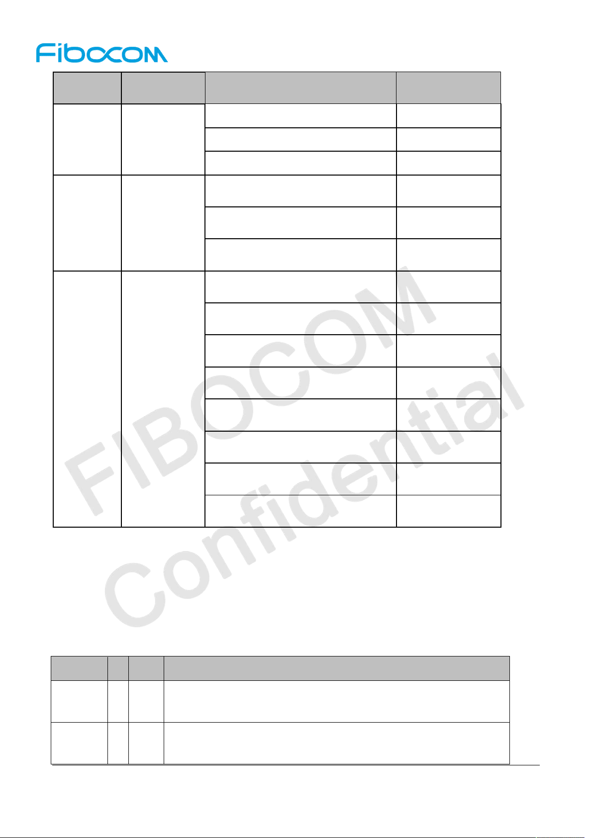
Table 3-4 VDD_EXT Logic Level
3.2.3 Power consumption
The power consumption of NL668-AM module in the case of 3.8V power supply is shown in the following
table.
Parameter Mode Condition
I
off
Power off
Power supply, module power off
WCDMA DRX=8
I
Idle
LTE FDD Paging cycle #256 frames
Average
Typ.Current(mA)
0.015
≤20
≤20
Radio Off AT+CFUN=4
DRX=6
I
sleep
WCDMA
DRX=7
DRX=8
DRX=9
Reproduction forbidden without Fibocom Wireless Inc. written authorization - All Rights Reserved.
FIBOCOM NL668-AM Hardware User Manual Page 24 of 62
≤15
≤3
≤3
≤3
≤3
Page 25
Parameter Mode Condition
Paging cycle #64 frames
FDD-LTE
Paging cycle #128 frames
Paging cycle #256 frames
WCDMA Data transfer Band II
@+23.5dBm
I
WCDMA-RMS
WCDMA
WCDMA Data transfer Band IV
@+23.5dBm
WCDMA Data transfer Band V
@+23.5dBm
LTE FDD Data transfer Band 2
@+23dBm
LTE FDD Data transfer Band 4
@+23dBm
LTE FDD Data transfer Band 5
@+23dBm
LTE FDD Data transfer Band 12
@+23dBm
I
LTE-RMS
LTE FDD
LTE FDD Data transfer Band 13
@+23dBm
LTE FDD Data transfer Band 17
@+23dBm
LTE FDD Data transfer Band 66
@+23dBm
LTE FDD Data transfer Band 71
@+23dBm
Average
Typ.Current(mA)
≤3
≤3
≤3
≤630
≤670
≤530
≤680
≤750
≤640
≤640
≤680
≤680
≤750
≤680
Table 3-5 Power Consumption
3.3 Control Signal
The NL668-AM module provides two control signals for power on/off and reset operations. The pin
definitions are as follows.
Pin name I/O Pin Description
RESET_N I 20
PWRKEY I 21
Reproduction forbidden without Fibocom Wireless Inc. written authorization - All Rights Reserved.
FIBOCOM NL668-AM Hardware User Manual Page 25 of 62
When the module is in work, give it a Tst (750ms~2s) low level, and then
pull it high, the module is reset
When module is in power off mode , give it a Tst (100ms~2s) low level,
and then pull it high, the module will power on; When module is in power
Page 26
Pin name I/O Pin Description
on mode, give it a Tst (2s~8s) low level, and then pull it high, the module
will power off
Table 3-6 Control Signal
3.3.1 Module power on
3.3.1.1 power on circuit reference
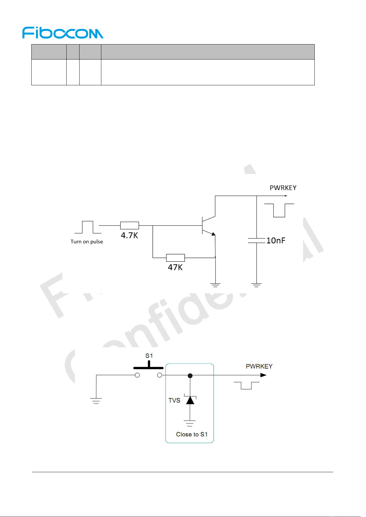
When the NL668-AM module is in power off mode, the module will power on by pulling down PWRKEY for
100ms~ 2s . It is recommended to use OC/OD drive circuit to control PWRKEY pin. The reference circuit
is shown in Figure 3-4:
Figure 3-4 OC/OD Drive Power on Reference Circuit
Another method to control PWRKEY pin is to directly control through a button, and place a TVS
(recommended:ESD9X5VL-2/TR) near the button for ESD protection.
The reference circuit is shown in Figure 3-5.
Figure 3-5 Button Power on Reference Circuit
Reproduction forbidden without Fibocom Wireless Inc. written authorization - All Rights Reserved.
FIBOCOM NL668-AM Hardware User Manual Page 26 of 62
Page 27
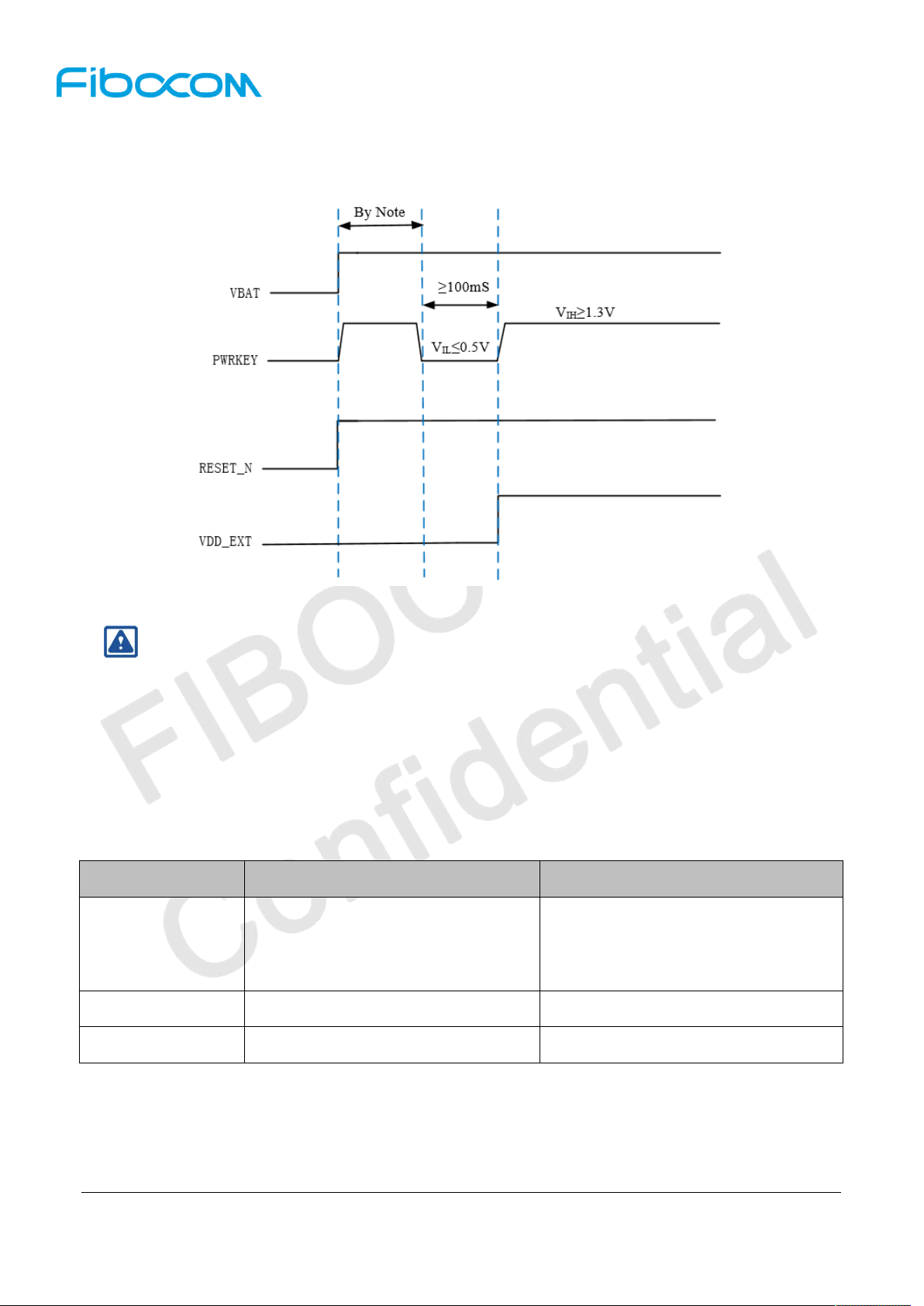
3.3.1.2 Power on Timing
The power on timing is shown in Figure 3-6:
Figure 3-6 Power on Timing Control Diagram
Note:
Before pulling down the PWRKEY pin, make sure the VBAT voltage is stable. It is recommended
that the interval between power up VBAT and pull down PWRKEY pin should not be less than
30ms.
3.3.2 Module power off
The module supports the following three power off modes:
Power off mode Power off methods Applicable scenarios
Low-voltage power
off
Hardware power off Pull down PWRKEY (2s~ 8s) Normal power off
When VBAT voltage is low or power
down, the module will power off
The module does not power off through
normal process, i.e. does not logout
process from the base station
AT power off
AT+ CPWROFF
Software power off
Table 3-7 Power Off Modes
3.3.2.1 Power off Timing
1. When the module is working properly, do not cut off the power of the module immediately to avoid
Reproduction forbidden without Fibocom Wireless Inc. written authorization - All Rights Reserved.
FIBOCOM NL668-AM Hardware User Manual Page 27 of 62
Page 28
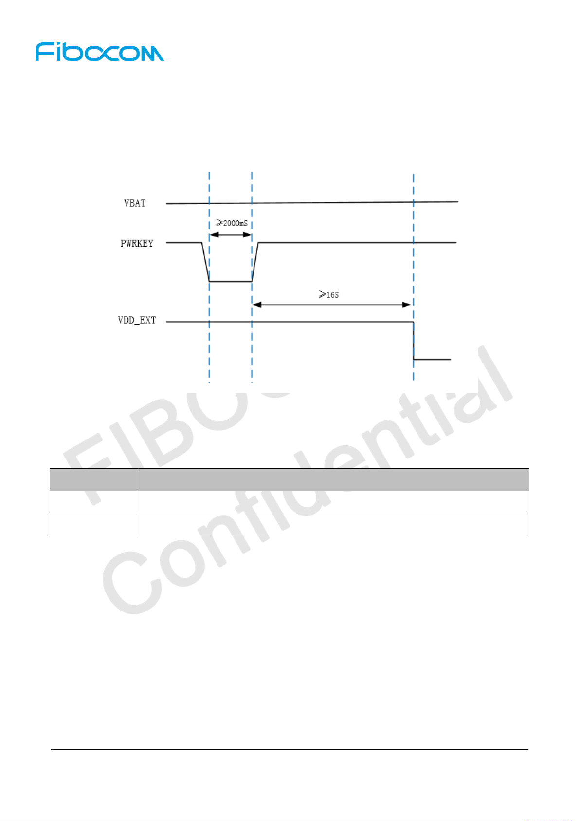
damaging the internal Flash . It is strongly recommended to power off the module by PWRKEY or AT
command before cut off the power supply.
2. When using the AT command to power off, make sure that the PWRKEY is in a high level state after the
power off command is executed, otherwise the module will power on again after the power off complete.
Figure 3-7 Power off Timing Control Diagram
3.3.3 Module reset
NL668-AMmodule can reset by hardware and AT command.
Reset mode Reset method
Hardware Pull down RESET_N about 750ms~2s and then pull up the level
AT command AT+RESET
Table 3-8 Module Reset
3.3.3.1 Reset circuit
Refer to Figure 3-8 reset circuit. It is similar to the PWRKEY control circuit. The client can control the
RESET_N pin using an OC/OD drive circuit or push button.
Reproduction forbidden without Fibocom Wireless Inc. written authorization - All Rights Reserved.
FIBOCOM NL668-AM Hardware User Manual Page 28 of 62
Page 29
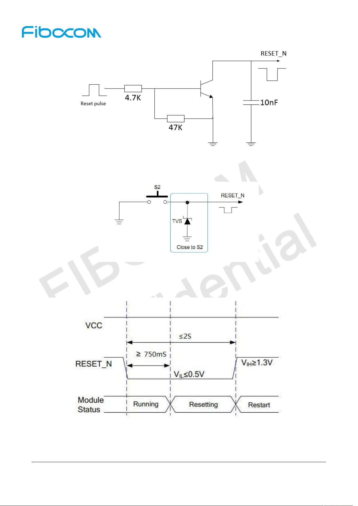
Figure 3-8 RESET_N OC/OD Drive Reference Circuit
Another reset control is shown in Figure 3-9.
Figure 3-9 RESET_N Button Reference Circuit
3.3.3.2 RESET control Timing
Figure 3-10 Reset Control Timing
Reproduction forbidden without Fibocom Wireless Inc. written authorization - All Rights Reserved.
FIBOCOM NL668-AM Hardware User Manual Page 29 of 62
Page 30
Note:
RESET is a sensitive signal, so it is recommended to add an avoid debouncing capacitor close
to the module. In case of PCB layout, the RESET signal lines should keep away from the RF
interference and protected by Ground. Also, the RESET signal lines shall neither near the PCB
edge nor route on the surface planes( avoid module reset caused by ESD problems).
3.4 USB Interface
The NL668-AM module supports USB2.0 and is compatible with USB High-Speed (480Mbits/s) and USB
Full-Speed (12Mbits/s). Refer to “Universal Serial Bus Specification 2.0” for the timing and electrical
characteristics of the NL668-AM module USB bus.
3.4.1 USB interface definition
Pin name I/O Pin Description
USB_DM I/O 70
USB_DP I/O 69
USB_VBUS PI 71
Table 3-9 USB Interface Definition
At present, USB just support USB_VBUS detect.
For more information about the USB 2.0 specification, please refer to http://www.usb.org/home
Note:
Since the module supports USB 2.0 High-Speed, TVS tube equivalent capacitance on the
USB_DM/DP differential signal cable is required to be less than 1pF, and a 0.5pF capacitance
TVS is recommended.
Connect a 0 ohm resistor to USB_DM / DP differential line to help analyze problems.
USB_DM and USB_DP are high-speed differential signal cables, can achieve the maximum
transmission rate of 480Mbits/s, and must follow the rules below in PCB Layout:
USB differential data bus ( D+ )
USB differential data bus ( D- )
USB_DET
USB_DM and USB_DP signal cable’s control differential impedance is 90 ohm
USB_DM and USB_DP signal cables shall be parallel and equal in length, and avoid the
right-angle route;
USB_DM and USB_DP signal cables are routed on the signal layer closest to the ground layer,
and the cables shall be grounded;
Reproduction forbidden without Fibocom Wireless Inc. written authorization - All Rights Reserved.
FIBOCOM NL668-AM Hardware User Manual Page 30 of 62
Page 31
3.5 USIM Interface
NL668-AM module has built-in USIM card interface, and supports 1.8V and 3.0V SIM card.
3.5.1 USIM pin
USIM pin is shown in the following table:
Pin name I/O Pin Description
USIM_DATA I/O 15 USIM/SIM DATA
USIM_CLK O 16 Clock Signal
USIM_RESET O 17 RESET Signal
USIM_VDD O 14 USIM/SIM Power
USIM_PRESENCE I 13 Detect USIM/SIM card for Hot-swap
Table 3-10 SIM Card Pin
3.5.2 USIM interface circuit
3.5.2.1 SIM card slot with detection signal
USIM/SIM design requires the use of SIM card slot (Fibocom recommend: SIM016-8P-220P). We
recommend using hot plug slot with SIM_DECTECT function.
Reproduction forbidden without Fibocom Wireless Inc. written authorization - All Rights Reserved.
FIBOCOM NL668-AM Hardware User Manual Page 31 of 62
Page 32
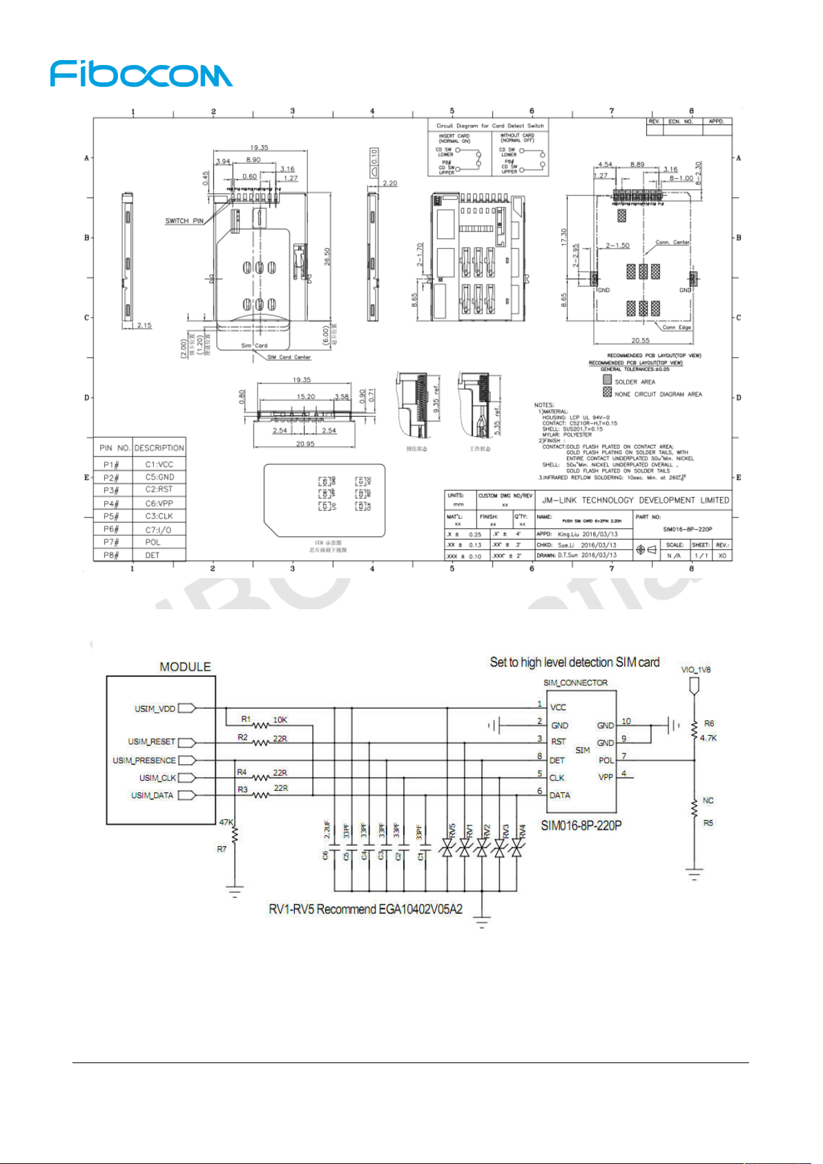
Figure 3-11 SIM Card Slot Diagram SIM016-8P-220P
Figure 3-12 USIM/SIM Interface with Detection Signal Reference Design
Principles of SIM card slot with detection signal are as follows:
SIM card is insert, USIM_PRESENCE pin is high level
SIM card is no insert, USIM_PRESENCE pin is low level
Reproduction forbidden without Fibocom Wireless Inc. written authorization - All Rights Reserved.
FIBOCOM NL668-AM Hardware User Manual Page 32 of 62
Page 33
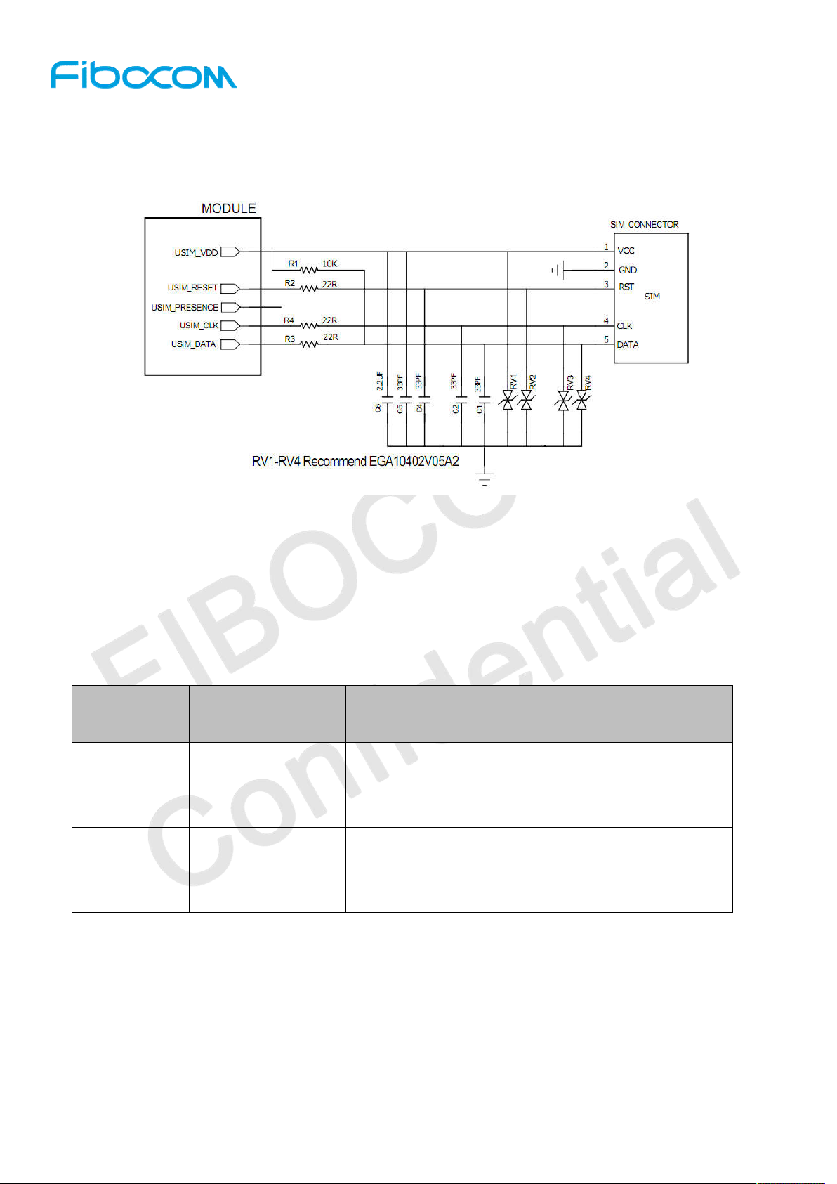
3.5.2.2 SIM card slot without detection signal
SIM card slot without detection signal, and USIM_ PRESENCE pin remains floating.
Figure 3-13 USIM/SIM Interface without Detection Signal Reference Design Diagram
3.5.3 USIM hot plug
NL668-AM SIM card supports hot plug function. It determines the insertion and removal of SIM card on
the slot by detecting the USIM_ PRESENCE pin state to support hot plug function.
The SIM card hot plug function can be configured by the “AT+MSMPD” command, and the AT commands
are shown in the following table:
AT command
AT+MSMPD=1 Enabled
AT+MSMPD=0 Disabled
SIM card hot plug
Function description
detection
Default, SIM card hot plug detection is enabled
The module detects whether the SIM card is inserted
through the USIM_PRESENCE pin state
SIM card hot plug detection function is disabled
The module reads the SIM card when the device starts,
and does not detect the USIM_PRESENCE state
Table 3-11SIM Card Hot Plug Function Configured AT Commands
After enabled the hot plug detection function of the SIM card, when USIM_PRESENCE is in high level,
the module will detect the SIM card insertion and then execute the initialization program of the SIM card.
After reading the SIM card information, the module will register network. When the USIM_PRESENCE is
in low level, the module detects that the SIM card is removed, then it will not read the SIM card.
Reproduction forbidden without Fibocom Wireless Inc. written authorization - All Rights Reserved.
FIBOCOM NL668-AM Hardware User Manual Page 33 of 62
Page 34
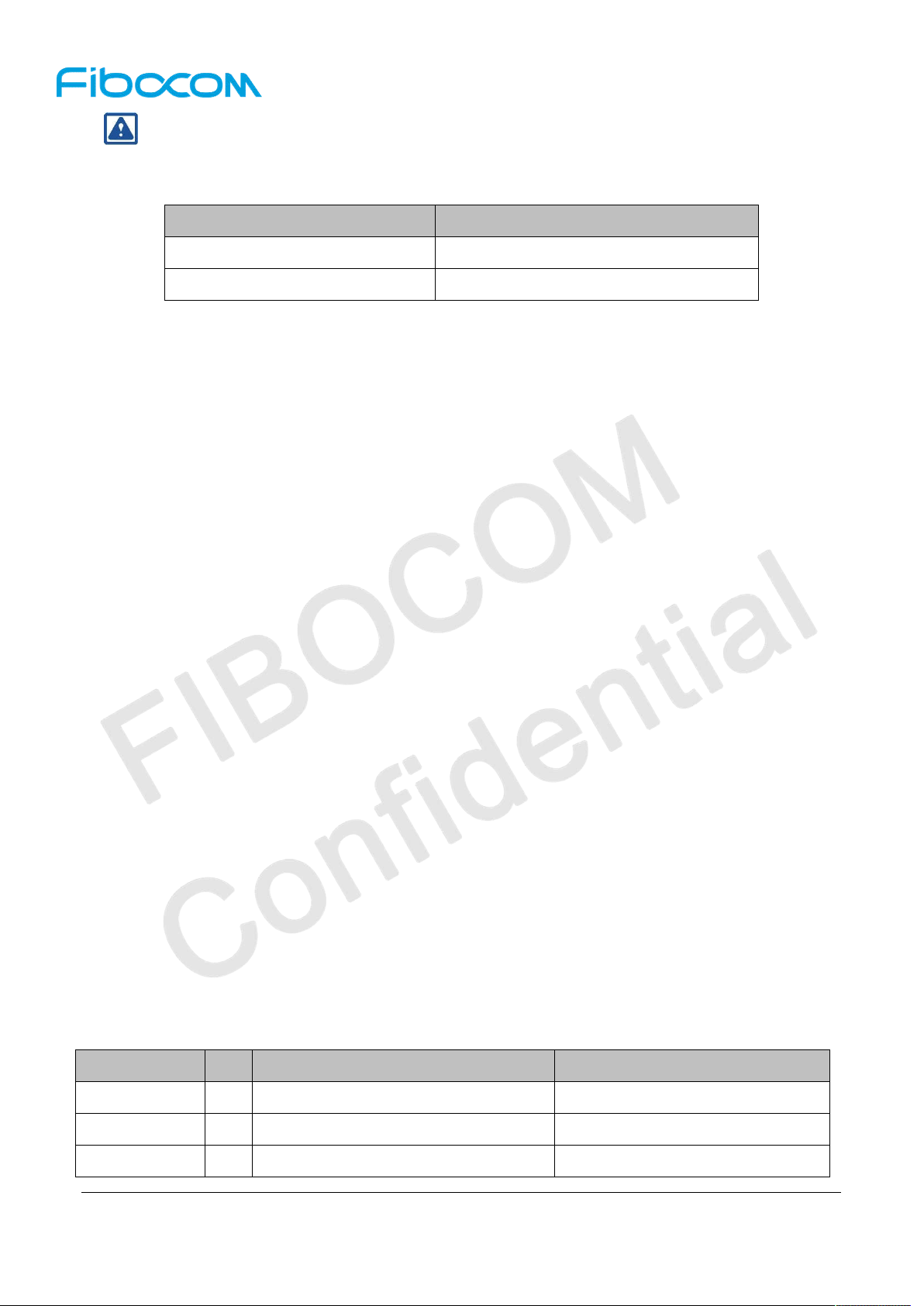
Note:
The USIM_PRESENCE is in active high by default, and can be switched to active low by AT
command.
AT command Function description
AT+GTSET=”SIMPHASE”,1 Default ,high level detect
AT+GTSET=”SIMPHASE”,0 Low level detect
Table 3-12 USIM_PRESENCE
Effective Level Switched AT command
3.5.4 USIM design requirements
SIM card circuit design shall meet EMC standards and ESD requirements, and at the same time, shall
improve anti-interference ability to ensure that the SIM card can work stably. The design needs to strictly
observe the following rules:
SIM card slot is placed as close to the module as possible, away from the RF antenna, DCDC power,
clock signal lines and other strong interference sources;
Adopt the SIM card slot with metal shield shell to improve anti-interference ability;
The length of cable from the module to the SIM card slot shall not exceed 100mm. Longer cable
reduces signal quality.
USIM_CLK and USIM_DATA signals are ground isolated to avoid mutual interference. If it is difficult
to do so, SIM signal needs to be ground protected as a set;
The filter capacitor and ESD device of SIM card signal cable are placed close to the SIM card slot.
Select 22 ~ 33pF capacitor for ESD device equivalent capacitor.
3.6 UART Interface
3.6.1 UART interface definition
NL668-AM module has two serial interfaces: the main serial interface and debug serial ports. The
following describes the main features of these two serial ports:
The main serial ports supports 4800bps, 9600bps, 19200bps, 38400bps, 57600bps, 115200bps,
230400bps, baud rate. The default baud rate is 115200bps, used for data transmission and AT command
transmission.
Debug serial port supports 115200bps baud rate for FIBOCOM debug.
The following table describes the main serial port pin.
Pin name I/O Pin Description
RI O 62 Ring indicator
DCD O 63 Data carrier detection
CTS I 64 Clear to send
Reproduction forbidden without Fibocom Wireless Inc. written authorization - All Rights Reserved.
FIBOCOM NL668-AM Hardware User Manual Page 34 of 62
Page 35
Pin name I/O Pin Description
RTS O 65 Request to send
DTR I 66 Sleep mode control
TXD O 67 Module Transmit data
RXD I 68 Module Receive data
Table 3-13 Main Serial Port Pin
The following table describes the debug serial interface pin.
Pin name I/O Pin Description
DBG_RXD
DBG_TXD
I 11 Module Receive data
O 12 Module Transmit data
Table 3-14 Debug Serial Port Pin
3.6.2 UART port application
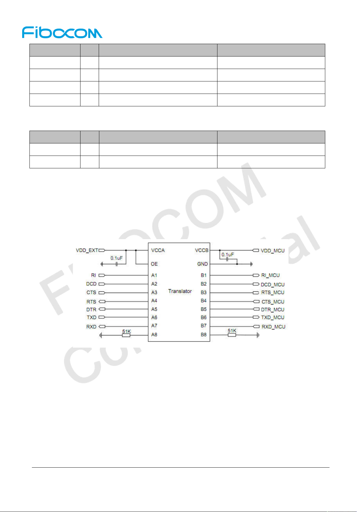
The serial port level of NL668-AM LCC module is 1.8V. If the level of the client host system is 3.3V or
other, a level
following figure shows the reference circuit design using level
translate
shall be added to the serial port connection between the module and the host. The
translate
chip:
Figure 3-14 UART Level Translate Reference Circuit 1
Another level
part can refer to that in the solid line part, but pay attention to the connection direction.
FIBOCOM NL668-AM Hardware User Manual Page 35 of 62
translate
Reproduction forbidden without Fibocom Wireless Inc. written authorization - All Rights Reserved.
circuit is shown below. The input and output circuit design in the following dashed
Page 36
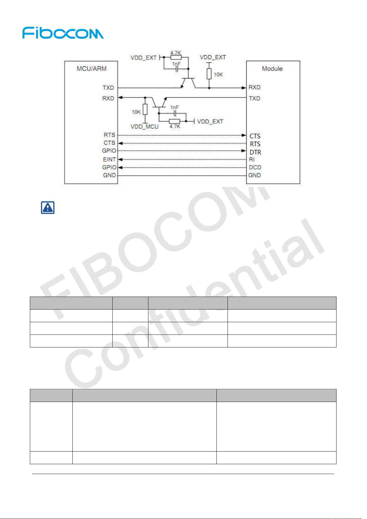
Figure 3-15 UART Level Translate Reference Circuit 2
Note:
This level translate circuit is not suitable for applications with baud rates above 460Kbps.
3.7 Status Indicator
NL668-AM provides three network indication pins (Pin 5 is network status indicator by default, AT
commands AT+LEDCFG can switch to pin 6 or pin 61).
PIN Name I/O PIN Num. Description
NET_MODE O 5 Network status indicator
NET_STATUS O 6 Reserved
STATUS O 61 Reserved
Table 3-15 Network Indication pins
3.7.1 NET_MODE Signal
NL668-AM module network indicator status description.
Mode NET_MODE Description
No SIM card
1
2
FIBOCOM NL668-AM Hardware User Manual Page 36 of 62
Flash (600ms High/600ms Low)
Slow flash (75ms Low /3000ms High) Standby
Reproduction forbidden without Fibocom Wireless Inc. written authorization - All Rights Reserved.
Request SIM PIN
Registering network (T<15S)
Register network failed
Page 37
Mode NET_MODE Description
3
4 Low Voice call
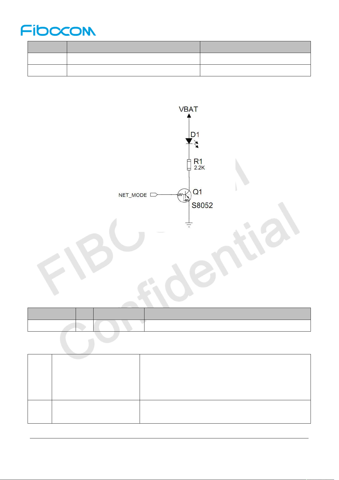
NL668-AM NET_MODE interface reference circuit is as shown below.
Speed flash (75ms Low /75ms High) Data link established
Table 3-16 Network Indicator Status Description
Figure 3-16 NET_MODE Reference Design Diagram
3.8 Low Power Mode
3.8.1 Flight mode
W_DISABLE# Pin Description:
Pin name
W_DISABLE# I
NL668-AM supports two ways to enter the flight mode:
1
Hardware I/O interface button
control
I/O Pin
4
Table 3-17 W_DISABLE# Pin Description
Description
Module flight mode control
First to transmit the “AT+WDISABLEEN=1”to enable the
W_DISABLE# function.
Pull high or float (pull high by default)the W_DISABLE# signal
to enter the normal mode, pull low it to enter the flight mode.
2
FIBOCOM NL668-AM Hardware User Manual Page 37 of 62
AT command control
Reproduction forbidden without Fibocom Wireless Inc. written authorization - All Rights Reserved.
AT+CFUN=0,0--enter the flight mode
AT+CFUN=1,0--enter the normal mode
Table 3-18 Module enter Fly Mode
Page 38

3.8.2 Sleep Mode
3.8.2.1 USB Application ( nonsupport USB Suspend, support VBUS)
If the host does not support the USB Suspend function, the module can enter sleep mode by
disconnecting USB_VBUS from the external control circuit:
Sleep:
Sent AT+GTLPMMODE=1,X command to set the WAKEUP_IN control enter the sleep mode. Reset the
module become effective. ( X=0, high level active to sleep; X=1, low level active to sleep)
AT+CSCLK = 1 command to enable sleep function.
AT+GTUSBSLEEPEN=1,0 command to set USB sleep mode
To draw out the USB line or disable the USB HUB controller to enter the sleep.
Wake up:
Wake up the module by plugging in the USB cable or enable the USB HUB controller.
3.8.2.2 USB application (nonsupport USB Suspend, nonsupport VBUS)
If the host does not supports USB Suspend and does not support VBUS function, the module can enter
sleep mode by disconnecting USB_VBUS from the external control circuit:
Sleep:
Sent AT+GTLPMMODE=1,X command to set the WAKEUP_IN control enter the sleep mode. Reset the
module become effective. ( X=0,high level active to sleep; X=1, low level active to sleep)
AT+CSCLK = 1 command to enable sleep function.
Use AT+GTUSBDETECTEN=1 command to enable the USB software detection
AT+GTUSBSLEEPEN=1,0 command to set USB sleep mode
To draw out the USB line or disable the USB HUB controller to enter the sleep.
Wake up:
Wake up the module by plugging in the USB cable or enable the USB HUB controller.
3.8.2.3 USB application (Supports USB Suspend)
If the host supports USB Suspend/Resume. Setting the USB into sleep by Linux.
Sleep:
Sent AT+GTLPMMODE=1,X command to set the WAKEUP_IN control enter the sleep mode. Reset the
module become effective. ( X=0,high level active to sleep; X=1,low level active to sleep)
AT+CSCLK = 1 command to enable sleep function.
AT+GTUSBSLEEPEN=0,0 command to set USB sleep mode
Reproduction forbidden without Fibocom Wireless Inc. written authorization - All Rights Reserved.
FIBOCOM NL668-AM Hardware User Manual Page 38 of 62
Page 39

In Linux environment, set the USB level and control to AUTO. Standing the module and host about 2
seconds, that will be in suspend mode.
Wake up:
Any operation on USB will wake up the module from sleep.
3.8.2.4 UART application ( WAKEUP_IN level control )
When host and NL668 module has connected through UART, use the following steps to make the module
enter sleep mode:
Sent AT+GTLPMMODE=1,X command to set the WAKEUP_IN control enter the sleep mode. Reset the
module become effective. ( X=0,high level active to sleep; X=1, low level active to sleep)
AT+CSCLK = 1 command to enable sleep function.
AT+GTUSBSLEEPEN=2,X command to disable USB function (X is an arbitrary value)
Wake up:
Wake up the module by set a signal contrary with sleep on WAKEUP_IN line.( X=0,low level active to be
recall;X=1,high level active to be recall)
3.8.2.5 UART application ( DTR level control )
When host and NL668 module has connected through UART, use the following steps to make the module
enter sleep mode:
Sent AT+GTLPMMODE=2,X command to set the DTR control enter the sleep mode. Reset the module
become effective. ( X=0, high level active to sleep; X=1, low level active to sleep)
AT+CSCLK = 1 command to enable sleep function.
AT+GTUSBSLEEPEN=2,X command to disable USB function (X is an arbitrary value)
Wake up the module by set a signal contrary with sleep on DTR line.( X=0, low level active to be recall;
X=1, high level active to be recall).
3.8.2.6 ATS24 Command
Set the module into sleep by ATS24 command . use the following steps:
Sleep:
Sent AT+GTLPMMODE=0
AT+GTUSBSLEEPEN=2,X command to disable USB function (X is an arbitrary value without 0)
ATS24=X command to into sleep after X seconds.(X is not zero)
Wake up:
Wake up the module by send the AT command fast.
Note:
Since the level of UART sleep power is different, power dissipation when use ATS24 command
Reproduction forbidden without Fibocom Wireless Inc. written authorization - All Rights Reserved.
FIBOCOM NL668-AM Hardware User Manual Page 39 of 62
Page 40
to enter sleep mode is higher than Pin control to enter sleep mode.
The ATS24 function cannot ensure the module must be in sleep after X seconds, if the timer over
and the module cant into sleep. It will try again.
If you want to use the RI signal to represent the state of the module, please refer to the
AT+GTWAKE command in the AT manual.
3.9 Digital audio interface PCM
NL668-AM provides a PCM interface for communication with digital audio devices such as an external
CODEC. Digital audio interface including PCM_CLK, PCM_SYNC, and PCM_IN / PCM_OUT.
3.9.1 Support model
NUM. Product model Description
1 NL668-AM-00 support
2 NL668-AM-01 support
Table 3-19 Support model
3.9.2 PCM interface definition
PIN Name I/O PIN Num. Description
PCM_IN I 24 PCM Input
PCM_OUT O 25 PCM Output
PCM_SYNC I/O 26 PCM Synchronous Signal
PCM_CLK I/O 27 PCM CLK
Table 3-20 PCM Interface Definition
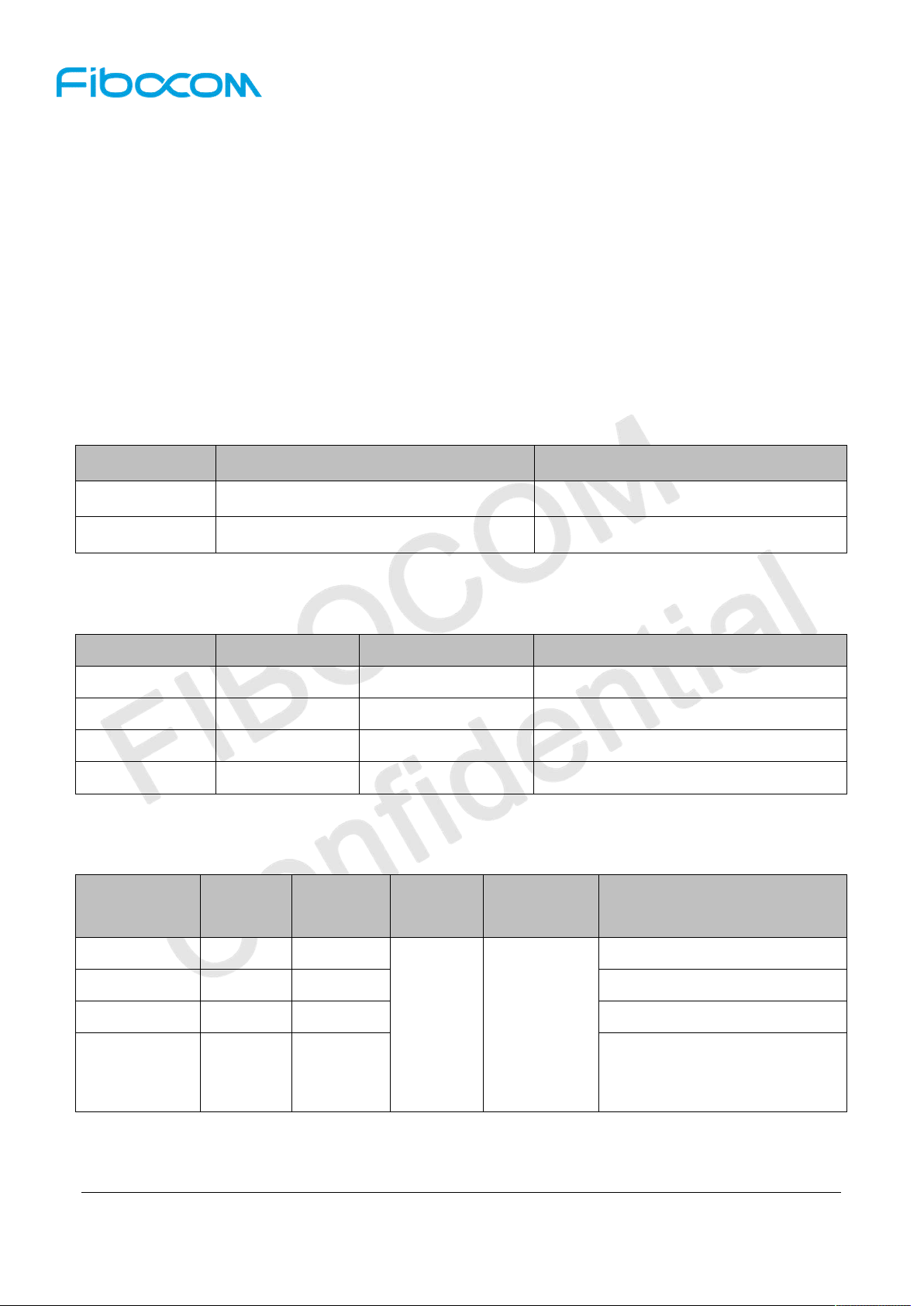
3.9.3 PCM interface description
Single Name
PCM_CLK 2.048MHz
PCM_OUT - - PCM Output
PCM_IN - - PCM Input
PCM_SYNC 8KHz BURST
Freq.
Duty
Cycle
50%
Coded
Format
16bit
Liner
mono
Operating
Mode
Module
serves as the
master that
supports
PCM slave
Description
PCM CLK
PCM Synchronous Signal
(Falling edge sampling)
Table 3-21 PCM Interface Description
NL668-AM adopts the above configuration by default, if you need to make adjustment, please contact our
Reproduction forbidden without Fibocom Wireless Inc. written authorization - All Rights Reserved.
FIBOCOM NL668-AM Hardware User Manual Page 40 of 62
Page 41
technical support.
3.9.4 PCM signal description
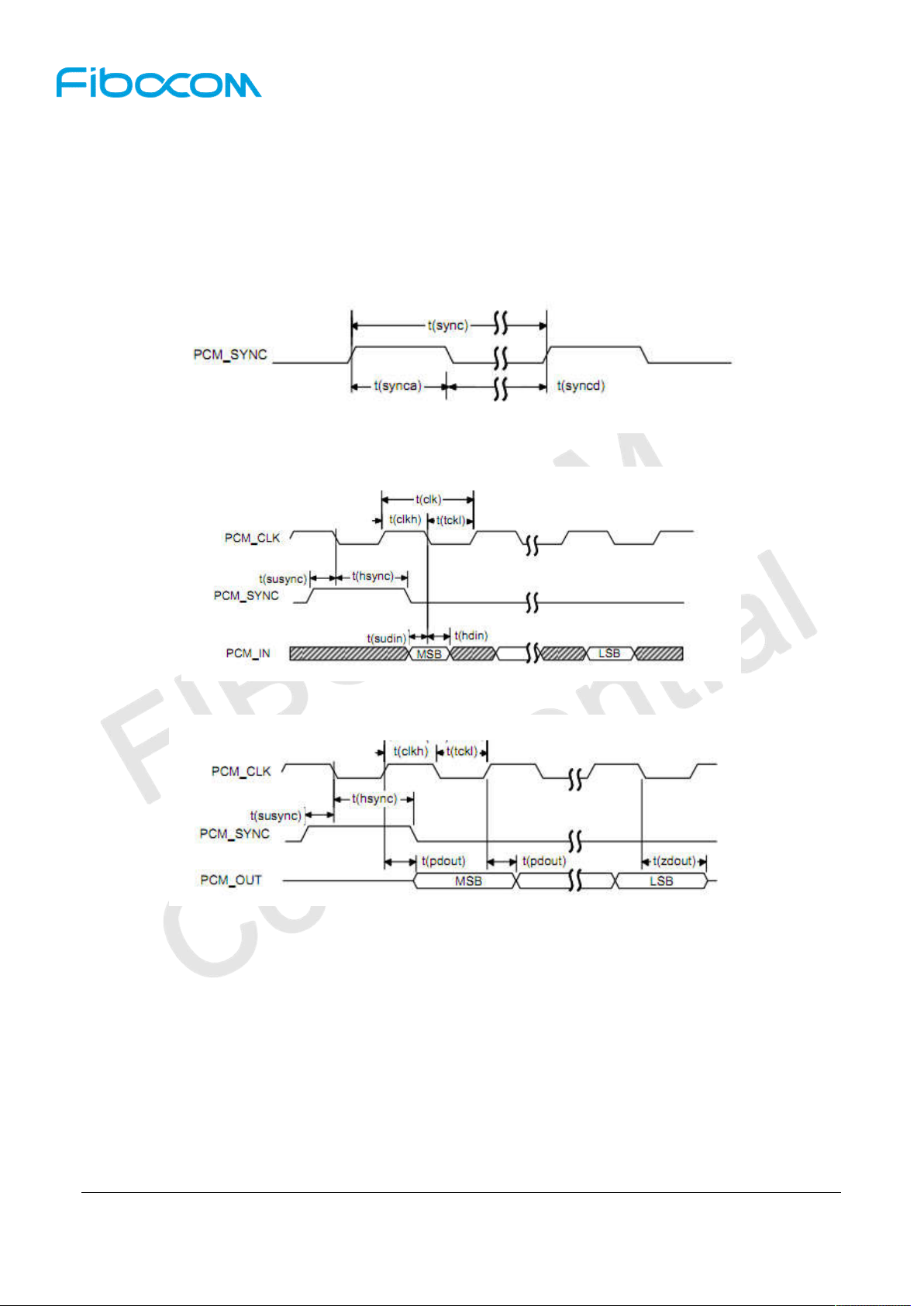
NL668-AM main chip support PCM signal adopts domestic mainstream Europe E1 standard. PCM_CLK
is a 2.048MHz clock in 16bit linear format encoding. PCM_SYNC is a 8kHz burst (488nS).
Figure 3-17 PCM_SYNC Timing
Figure 3-18 PCM_CODEC to NL668-AM Timing
Figure 3-19 NL668-AM to PCM_CODEC Timing
Reproduction forbidden without Fibocom Wireless Inc. written authorization - All Rights Reserved.
FIBOCOM NL668-AM Hardware User Manual Page 41 of 62
Page 42
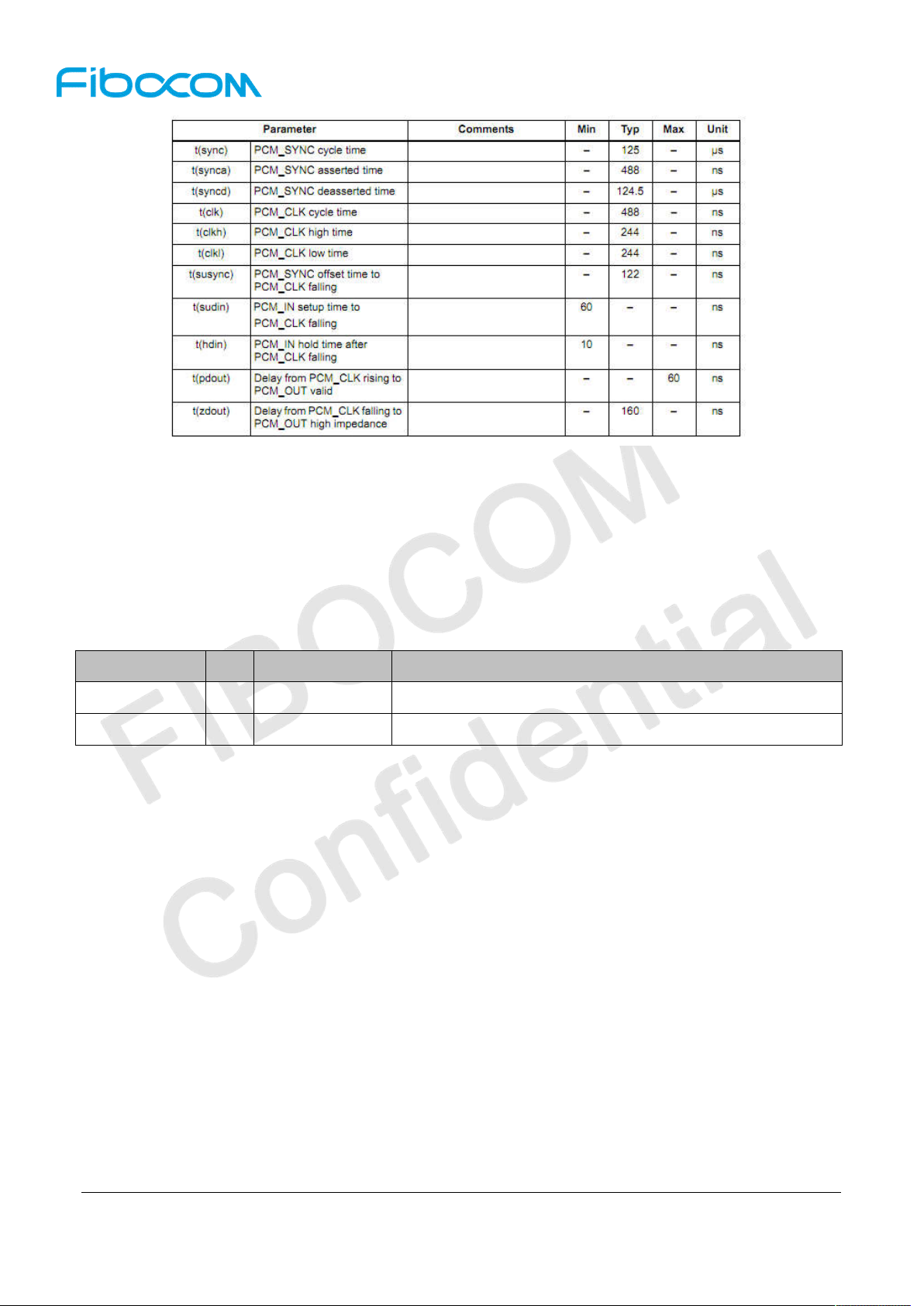
Figure 3-20 CODEC Timing Parameters
3.10 ADC function
NL668-AM support the 2 channels ADC interface. Use AT+TADC=0 to read the value on the ADC0
interface. Use AT+TADC=1 to read the value on the ADC1 interface. The ADC range is 0.3V-VBAT_BB.
PIN Name I/O PIN NUM. Description
ADC0 I
ADC1 I
45 Analog to digital converter interface 0
44 Analog to digital converter interface 1
Table 3-22 ADC Interface
Reproduction forbidden without Fibocom Wireless Inc. written authorization - All Rights Reserved.
FIBOCOM NL668-AM Hardware User Manual Page 42 of 62
Page 43
4 RF Interface
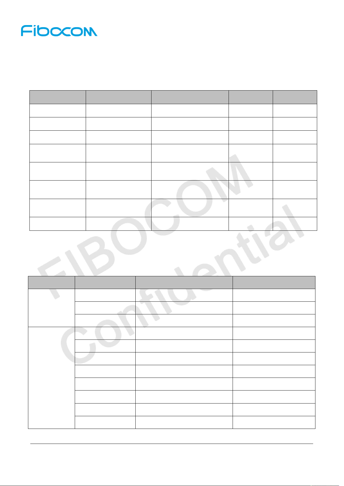
4.1 NL668-AM Operating Frequency
Operating Band Description Mode Tx (MHz) Rx (MHz)
Band 2 PCS 1900MHz LTE FDD/WCDMA 1850- 1910 1930 - 1990
Band 4 AWS-1 1700 LTE FDD/WCDMA 1710 - 1755 2110 - 2155
Band 5 CLR 850MHz LTE FDD/WCDMA 824 - 849 869 - 894
Band 12
Band 13
Band 17
Band 66
Band 71 US 600 LTE FDD 663-698 617-652
Lower SMH blocks
A/B/C 700
Lower SMH blocks
A/B/C 700
Lower SMH
(Blocks B–C)
Extended AWS-1
(Blocks A–I)
Table 4-1Operating Frequency
LTE FDD 699-716 729-746
LTE FDD 777-787 746-756
LTE FDD 704-716 734-746
LTE FDD 1710-1780 2110 - 2200
4.2 RF Output Power of NL668-AM
The RF output power of NL668-AM is shown in the following table.
Mode Band Tx Power(dBm) Note
Band II 23.5±1
WCDMA
Band IV 23.5±1
Band V 23.5±1
Band 2 23±1 10MHz Bandwidth, 1 RB
Band 4 23±1 10MHz Bandwidth, 1 RB
Band 5 23±1 10MHz Bandwidth, 1 RB
Band 12 23±1 10MHz Bandwidth, 1 RB
LTE FDD
Band 13 23±1 10MHz Bandwidth, 1 RB
Band 17 23±1 10MHz Bandwidth, 1 RB
Band 66 23±1 10MHz Bandwidth, 1 RB
Band 71 23±1 10MHz Bandwidth, 1 RB
Table 4-2 RF Output Power
Reproduction forbidden without Fibocom Wireless Inc. written authorization - All Rights Reserved.
FIBOCOM NL668-AM Hardware User Manual Page 43 of 62
Page 44
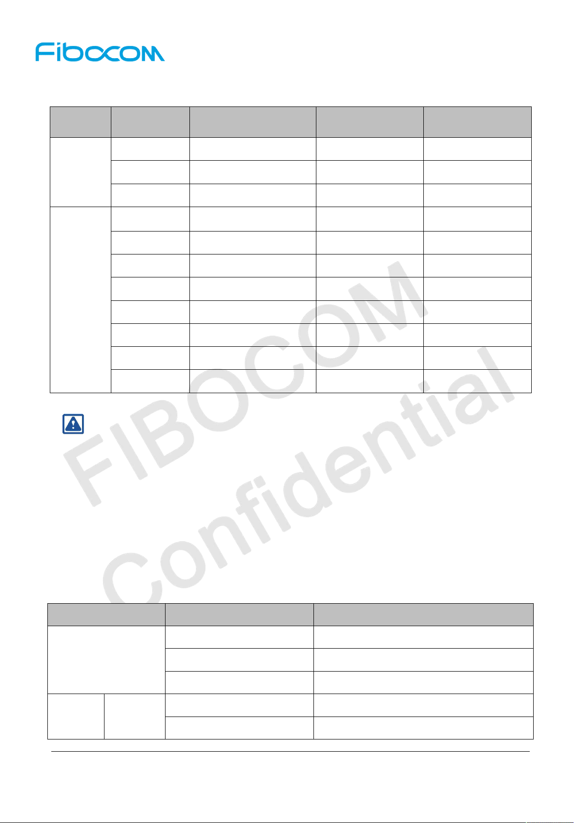
4.3 RF Receiving Sensitivity of NL668-AM
Mode Band
Band II -109 NA BER<0.1%
WCDMA
LTE FDD
Band IV -109.5 NA BER<0.1%
Band V -111 NA BER<0.1%
Band 2 -97.8 -98.5 10MHz Band width
Band 4 -97.8 -98 10MHz Band width
Band 5 -99 -100 10MHz Band width
Band 12 -98 -99 10MHz Band width
Band 13 -97 -99 10MHz Band width
Band 17 -98 -98 10MHz Band width
Band 66 -97.8 -98 10MHz Band width
Band 71 -98 -99 10MHz Band width
Rx Sensitivity(dBm)
PRX Typ.
Rx Sensitivity(dBm)
DRX Typ.
Note
Table 4-3 RF Receiving Sensitivity
Note:
The sensitivity in the above table is the result of test conducted with the main and diversity dual
antenna. If only the main antenna is used (without the diversity antenna), the sensitivity of each
band of LTE will be reduced by about 3dBm.
4.4 GNSS Receiver
4.4.1 Basic description
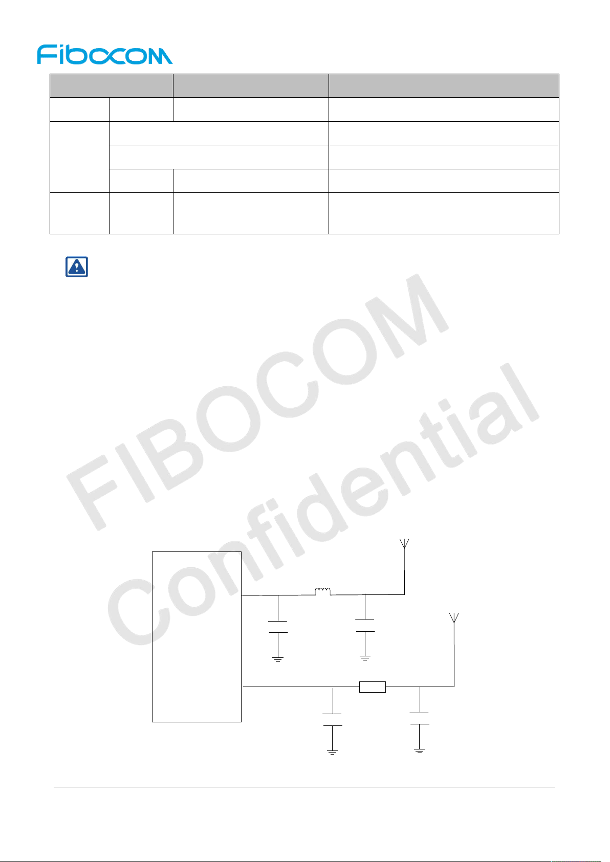
The NL668-AM module supports the GPS/GLONASS/BeiDou functions using Qualcomm Gen8
technology.
Description Condition Typ.
GNSS fixing 68mA
Current consumption
GNSS tracking
(AT+CFUN=0)
Standby
68mA
33mA
Cold start
TTFF GNSS
Warm start
Reproduction forbidden without Fibocom Wireless Inc. written authorization - All Rights Reserved.
FIBOCOM NL668-AM Hardware User Manual Page 44 of 62
40s
37s
Page 45
Description Condition Typ.
4s
-147dbm
-158dbm
38.5dB-HZ
Sensitivity
Hot Start
fixing
tracking
CN0 GNSS Signal@-130dBm
Positional
CEP GNSS Signal @-130dBm <4m
Accuracy
Table 4-4 GNSS Receiver
Note:
The current in above table test with USB plug in.
4.5 RF PCB Design
4.5.1 Antenna RF connector
The NL668-AM three-way antenna adopts the pad-out way. It is recommended that clients use the
U.FL-R-SMT-1 antenna connector and the matching RF adapter cable.
Antenna is a sensitive device, susceptible to the external environment. For example, the location of the
antenna, the space it occupies, and the surrounding ground all may affect antenna performance. In
addition, the RF cable connecting the antenna, and the location of the fixed antenna also may affect the
performance of the antenna.
Figure 4-1 is the reference circuit design for the main and diversity antenna. These matches need to be
placed close to the antenna:
MAIN
Antenna
Module
ANT_MAIN
ANT_DIV
C1
NA
C3
NA
R1
2nH
C2
NA
0R
NA
DIV
Antenna
R2
0R
C4
NA
Figure 4-1RF Reference Circuit Design
Reproduction forbidden without Fibocom Wireless Inc. written authorization - All Rights Reserved.
FIBOCOM NL668-AM Hardware User Manual Page 45 of 62
Page 46
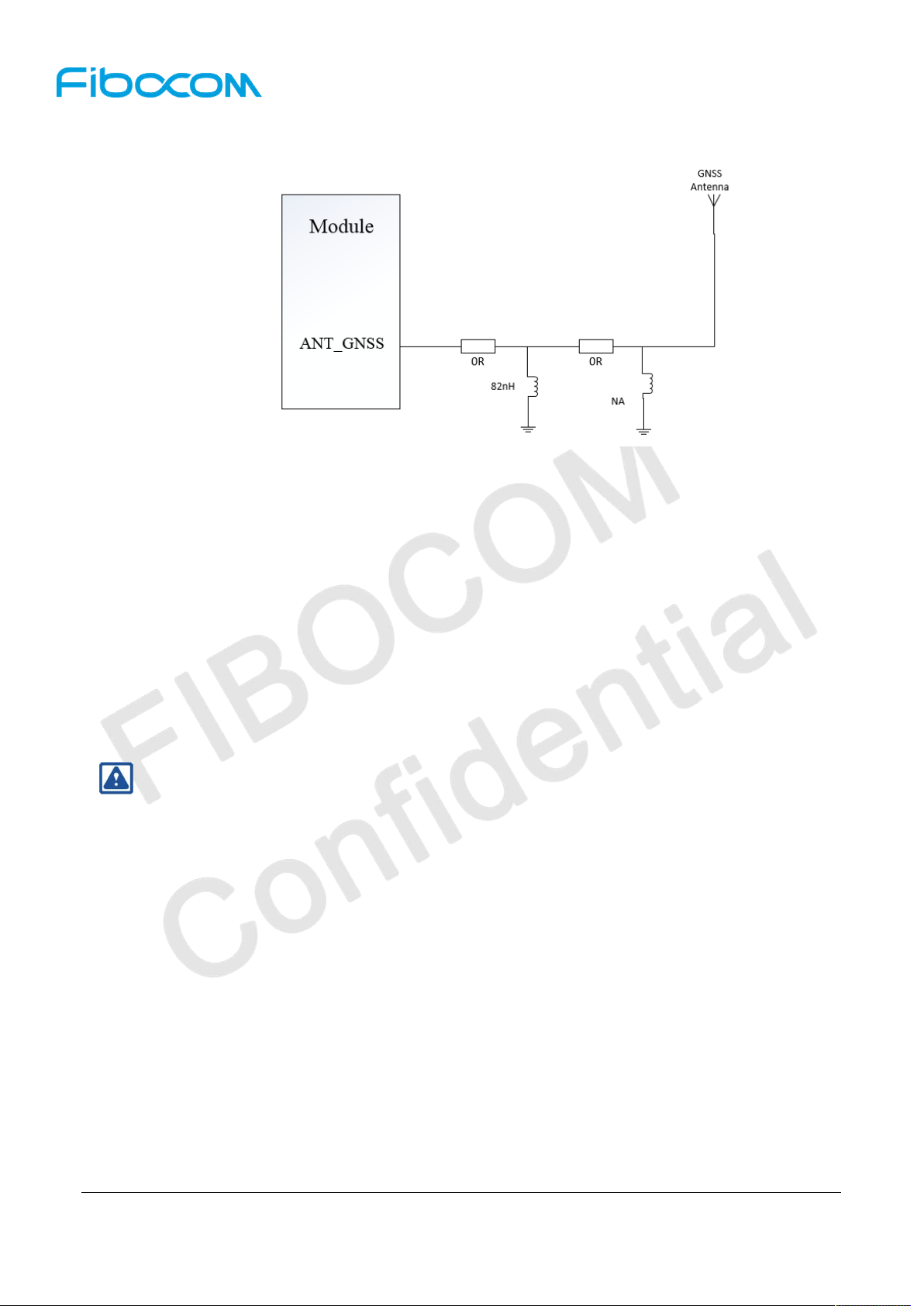
Figure 4-2 shows the reference circuit design for the GNSS antenna. These matches need to be placed
close to the antenna:
Figure 4-2 GNSS RF Reference Circuit
Make sure the characteristic impedance of the transmission cable is 50 ohms.
Since the antenna cable loss is less than 0.3dB, keep the PCB cable as short as possible.
Keep the PCB LAYOUT as straight as possible, and reduce holes on the route to another layer; also
avoid right-angle and acute-angle wiring.
PCB cable should have a good reference ground to avoid other signal cable near the antenna.
Recommend a complete ground level, and use this complete ground level as a reference ground.
The ground around the antenna must be connected to the main ground through the holes placed near the
edge of the ground and tracking the cable route.
Note:
Refer to the document《FIBOCOM_RF Antenna Application Design Instruction》for specific
design
4.6 Antenna Design
1) Antenna efficiency
Antenna efficiency is the ratio of antenna input power to emissivity. Due to the antenna return loss,
material loss, and coupling loss, the radiated power is always lower than the input power. Recommend>
40% (-4dB).
2) S11 or VSWR
S11 shows that the matching degree of the antenna’s 50 ohm impedance, to a certain extent, affects the
antenna efficiency. VSWR test methods can be used to measure this parameter. Recommend S11
<-10dB.
Reproduction forbidden without Fibocom Wireless Inc. written authorization - All Rights Reserved.
FIBOCOM NL668-AM Hardware User Manual Page 46 of 62
Page 47
3) Polarization
Polarization is the rotation direction of the electric field in the maximum radiation direction of the antenna.
It is recommended to use linear polarization.
4) Radiation pattern
Radiation pattern refers to the antenna’s electromagnetic field strength in the far field in all directions.
Half-wave dipole antenna is the most suitable terminal antenna. For built-in antenna, PIFA antennas or
IFA antennas are recommended:
Antenna area: 6mm high*10mm wide*100mm long.
Antenna radiation direction: Omni_directional.
5) Gain and directivity
Antenna directivity refers to the electromagnetic field strength of electromagnetic wave in all directions.
Gain is a collection of antenna benefits and antenna directivity.
Recommended antenna gain ≤2.5dBi.
6) Interference
In addition to the antenna performance, other interferences on the PCB also may affect the performance
of the module. In order to ensure the high performance of the module, interference must be controlled.
Suggestions: For example, LCD, CPU, FPC cable, audio circuit, power supply should be as far as
possible away from the antenna, and make the appropriate isolation and shielding, or filtering on the path.
7) Antenna index requirements
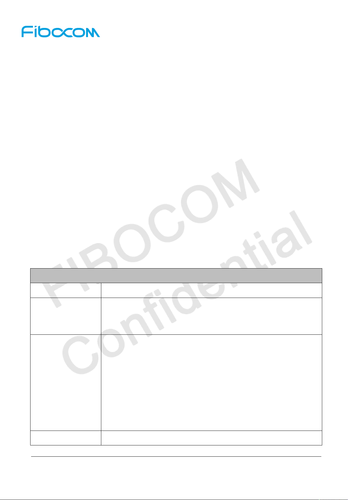
NL668-AM module main antenna requirements
Frequency range It must use the most suitable antenna to adapt to the relevant frequency band
WCDMA band II(1900) : 170 MHz
Bandwidth (WCDMA)
WCDMA band IV(1700) :170 MHz
WCDMA band V(850) : 70 MHz
LTE band 2(1900): 140 MHz
LTE Band 4(1700): 445 MHz
LTE Band 5(850): 70 MHz
LTE Band 12(700): 47 MHz
Bandwidth (LTE)
LTE band 17(700): 42 MHz
LTE band 13(700): 41 MHz
LTE Band 66(1700): 470MHz
LTE band 71(600): 81MHz
Impedance 50 ohms
Reproduction forbidden without Fibocom Wireless Inc. written authorization - All Rights Reserved.
FIBOCOM NL668-AM Hardware User Manual Page 47 of 62
Page 48
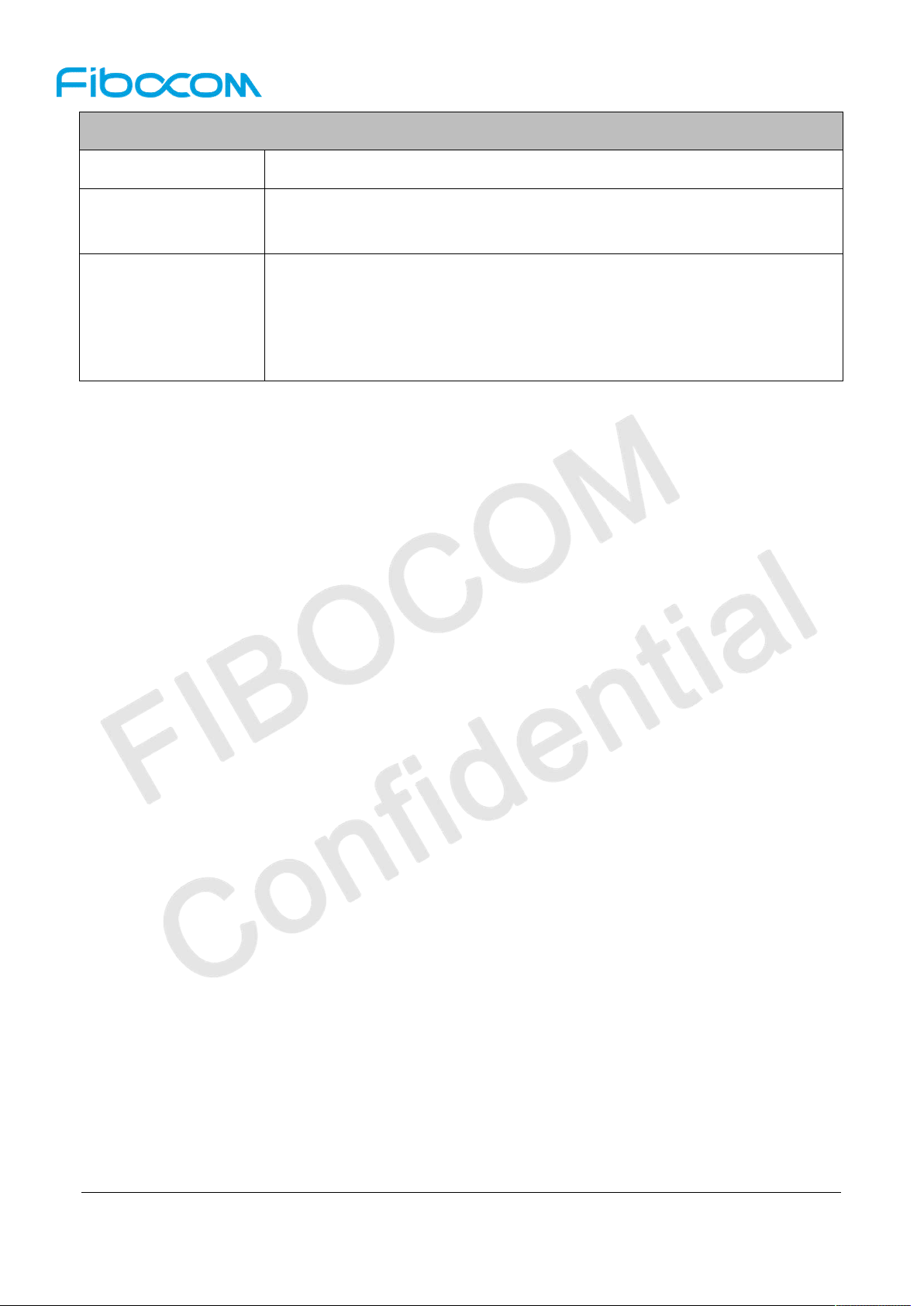
NL668-AM module main antenna requirements
Input power > 23dBm average power WCDMA & LTE
Standing wave ratio
recommended
GNSS
≤ 2:1
Frequency range: 1559MHz~1607MHz
Polarization type: right-circular or linear polarization
VSWR::< 2(Type)
Passive antenna gain:> 0dBi
Table 4-5 Main Antenna Requirement
Reproduction forbidden without Fibocom Wireless Inc. written authorization - All Rights Reserved.
FIBOCOM NL668-AM Hardware User Manual Page 48 of 62
Page 49
5 Electrical Characteristics
5.1 Limiting voltage range
The limiting voltage range refers to the power voltage of the module and the maximum voltage range that
the digital and analog input/output interfaces can withstand.
The voltage range of NL668-AM is shown in the following table.
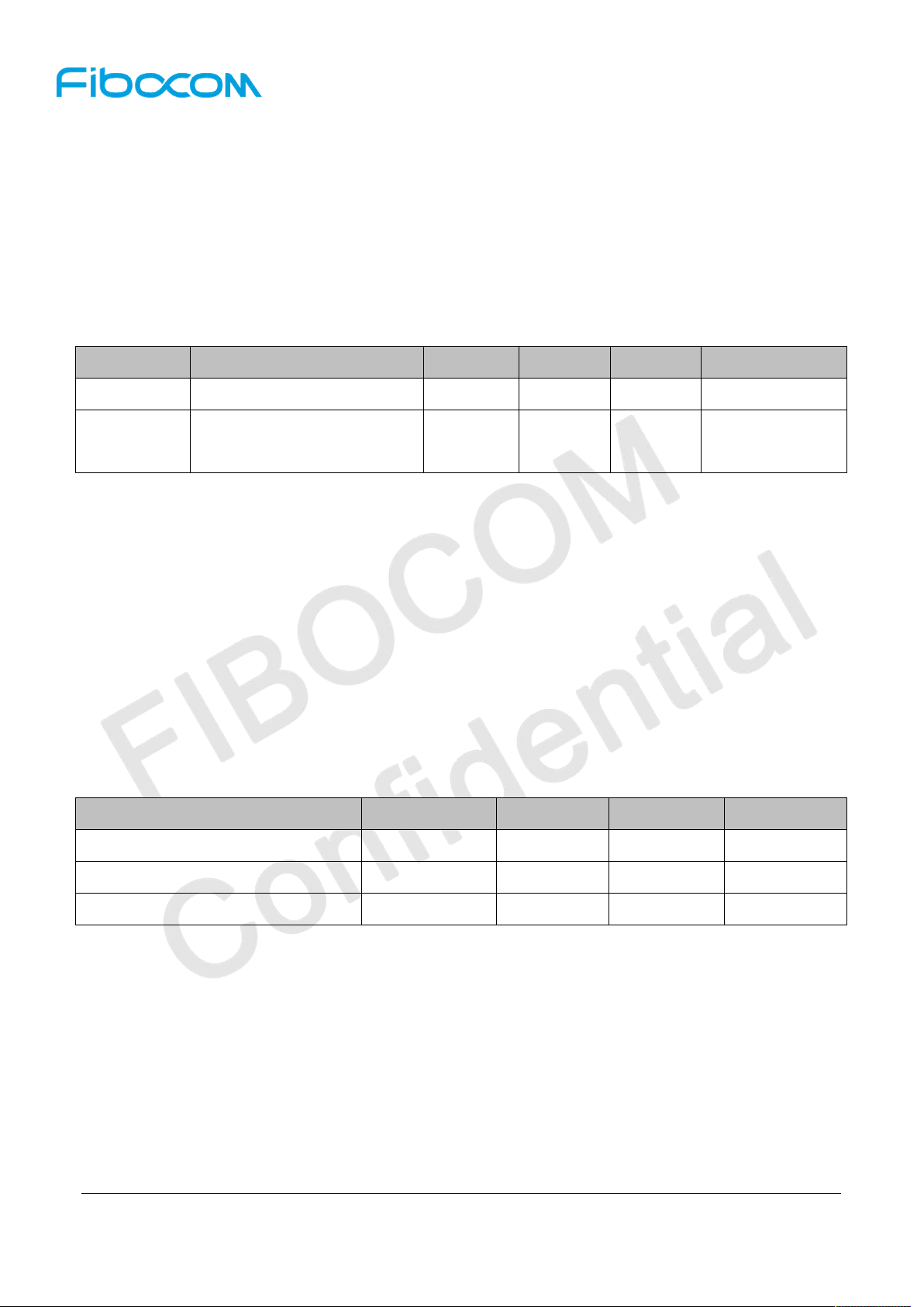
Parameter Description Min Typ Max Unit
VBAT Power supply -0.3 - 4.7 V
GPIO
Power supply voltage of
-0.3 - 2.0 V
digital I/O
Table 5-1 Voltage Range
5.2 Environment temperature range
NL668-AM module is recommended to operate at -30~+75℃ ambient. It is recommended that the
application uses temperature control measures under harsh environmental conditions. At the same time,
the limited operating temperature range of the module should be provided. Under these temperature
conditions, some RF parameters may exceed the limit. It is recommended that the module application
terminal be stored in certain temperature conditions. Modules outside this range may not operate or may
be damaged.
Temperature Min Typ Max Unit
Operating temperature -30 25 75 ℃
Limited operating temperature -40 85 ℃
Storage temperature -40 85 ℃
Table 5-2Environment Temperature Range
5.3 Electrical characteristics of the interface in
operating status
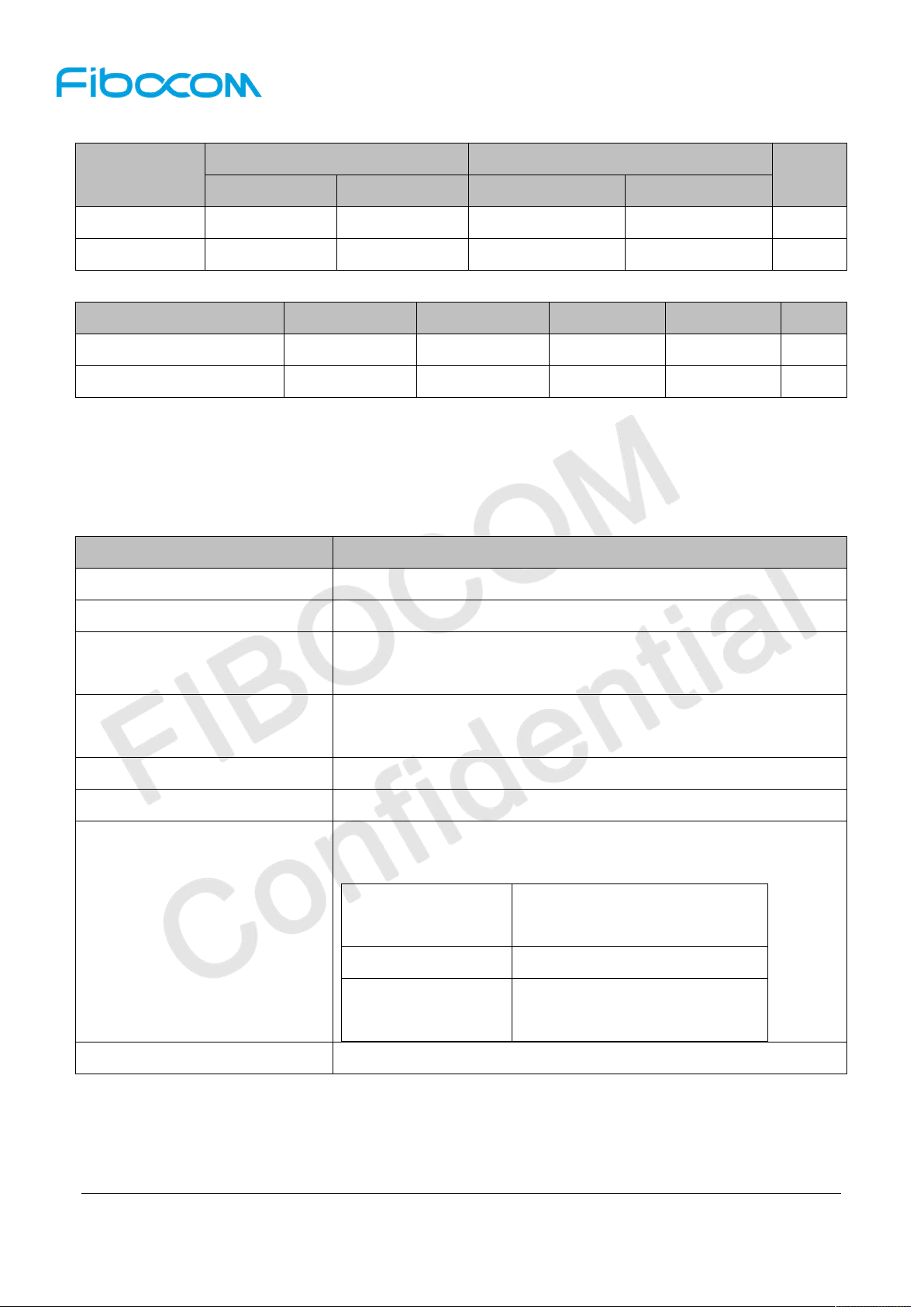
VL: logic low level;
VH: logic high level;
Reproduction forbidden without Fibocom Wireless Inc. written authorization - All Rights Reserved.
FIBOCOM NL668-AM Hardware User Manual Page 49 of 62
Page 50
VL VH
Signal
Min Max Min Max
Digital input -0.3 0.6 1.2 2.0 V
Digital output - 0.45 1.35 - V
Parameter I/O Min Typ Max Unit
VBAT I 3.3 3.8 4.3 V
SIM_VDD O 1.7/2.75 1.8/2.85 1.9/2.95 V
Table 5-3 Electrical Characteristics of the Interface in Operating Status
Unit
5.4 Environmental reliability requirements
Test items Test conditions
Low temperature storage test Temperature -40℃±3℃, 24 hours in shutdown state
High temperature storage test Temperature +85℃±3℃, 24 hours in shutdown state
In shutdown state, 0.5 hour at -40℃ and +85℃ environment
Temperature shock test
High temperature and humidity
test
Low temperature operating test Temperature -30℃±3℃, 24 hours in operating state
High temperature operating test Temperature +75℃±3℃, 24 hours in operating state
Vibration test
respectively, the temperature conversion time <3min, for 24 cycles
Temperature +85℃±3℃, humidity 90 ~ 95% RH, 24 hours in
shutdown state
Conduct vibration test according to the requirements shown in the
table below:
Frequency Random vibration ASD
(Acceleration Spectral Density)
5~20Hz 0.96m2/s3
20~500Hz 0.96m2/s3(20Hz), other
-3dB/octave
Connector life test 30 times of insertion/removal for RF antenna interface cable
Table 5-4 Environmental Reliability Requirements
Reproduction forbidden without Fibocom Wireless Inc. written authorization - All Rights Reserved.
FIBOCOM NL668-AM Hardware User Manual Page 50 of 62
Page 51
5.5 ESD characteristics
NL668-AM is a consumer product. Although the design of the module has considered the ESD issue and
provided ESD protection, the ESD issue may occur in the transport and secondary development, so
developers should consider ESD protection for the final product. In addition to considering anti-static
treatment for packaging, please refer to recommended circuit for interface design in the document for
client’s application.
Refer to the following table for the ESD allowable discharge range of the NL668-AM module.
Part Air discharge Contact discharge
VBAT,GND ±10KV ±5KV
Antenna interface ±8KV ±4KV
Other interface ±1KV ±0.5KV
Table 5-5 ESD Allowable Discharge Range
Reproduction forbidden without Fibocom Wireless Inc. written authorization - All Rights Reserved.
FIBOCOM NL668-AM Hardware User Manual Page 51 of 62
Page 52
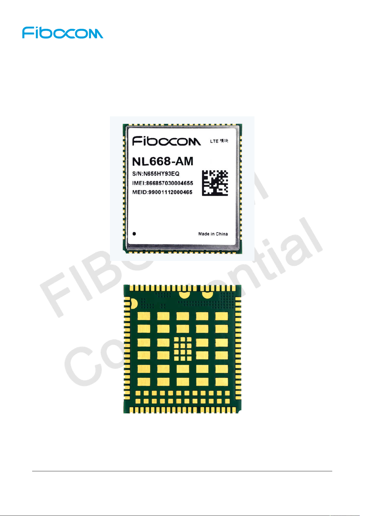
6 Structure Specification
6.1 Product Appearance
The product appearance for NL668-AM module is shown in Figure 6-1 and 6-2:
Figure 6-1Module Product Appearance (Top)
Figure 6-2 Module Product Appearance (Bottom)
Reproduction forbidden without Fibocom Wireless Inc. written authorization - All Rights Reserved.
FIBOCOM NL668-AM Hardware User Manual Page 52 of 62
Page 53
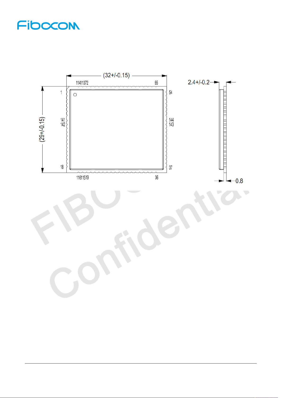
6.2 Dimension of Structure
The structural dimension of the NL668-AM module is shown in Figure 6-3:
Figure 6-3 Dimension of Structure (Unit: mm)
6.3 SMT Patch
For module stencil design, please refer to FIBOCOM_ NL668 LCC SMT Application Design Instruction.
Reproduction forbidden without Fibocom Wireless Inc. written authorization - All Rights Reserved.
FIBOCOM NL668-AM Hardware User Manual Page 53 of 62
Page 54
Appendix A Terms and Acronyms
Terms Description
AMR Adaptive Multi-rate
BPS Bits Per Second
CS Coding Scheme
DRX Discontinuous Reception
EGSM Extended GSM900 Band
FDD Frequency Division Duplexing
GMSK Gaussian Minimum Shift Keying
GSM Global System for Mobile Communications
HSDPA High Speed Down Link Packet Access
IMEI International Mobile Equipment Identity
Imax Maximum Load Current
LED Light Emitting Diode
LSB Least Significant Bit
LTE Long Term Evolution
SCell Secondary Cell for CA
ME Mobile Equipment
MS Mobile Station
MT Mobile Terminated
PCB Printed Circuit Board
PDU Protocol Data Unit
PSK Phase Shift Keying
Reproduction forbidden without Fibocom Wireless Inc. written authorization - All Rights Reserved.
FIBOCOM NL668-AM Hardware User Manual Page 54 of 62
Page 55
Terms Description
QAM Quadrature Amplitude Modulation
QPSK Quadrature Phase Shift Keying
RF Radio Frequency
RHCP Right Hand Circularly Polarized RMS
RMS Root Mean Square
RTC Real Time Clock
Rx Receive
SMS Short Message Service
TDMA Time Division Multiple Access
TE Terminal Equipment
TX Transmitting Direction
TDD Time Division Duplexing
UART Universal Asynchronous Receiver & Transmitter
UMTS Universal Mobile Telecommunications System
URC Unsolicited Result Code
(U)SIM (Universal) Subscriber Identity Module
USSD Unstructured Supplementary Service Data
V
Maximum Voltage Value
max
V
Normal Voltage Value
norm
V
Minimum Voltage Value
min
V
V
V
FIBOCOM NL668-AM Hardware User Manual Page 55 of 62
Maximum Input High Level Voltage Value
IHmax
Minimum Input High Level Voltage Value
IHmin
Maximum Input Low Level Voltage Value
ILmax
Reproduction forbidden without Fibocom Wireless Inc. written authorization - All Rights Reserved.
Page 56
Terms Description
V
Minimum Input Low Level Voltage Value
ILmin
V
Absolute Maximum Input Voltage Value
Imax
V
Absolute Minimum Input Voltage Value
Imin
V
V
V
V
Maximum Output High Level Voltage Value
OHmax
Minimum Output High Level Voltage Value
OHmin
Maximum Output Low Level Voltage Value
OLmax
Minimum Output Low Level Voltage Value
OLmin
VSWR Voltage Standing Wave Ratio
WCDMA Wideband Code Division Multiple Access
Table A-0-1 Terms and Acronyms
Reproduction forbidden without Fibocom Wireless Inc. written authorization - All Rights Reserved.
FIBOCOM NL668-AM Hardware User Manual Page 56 of 62
Page 57
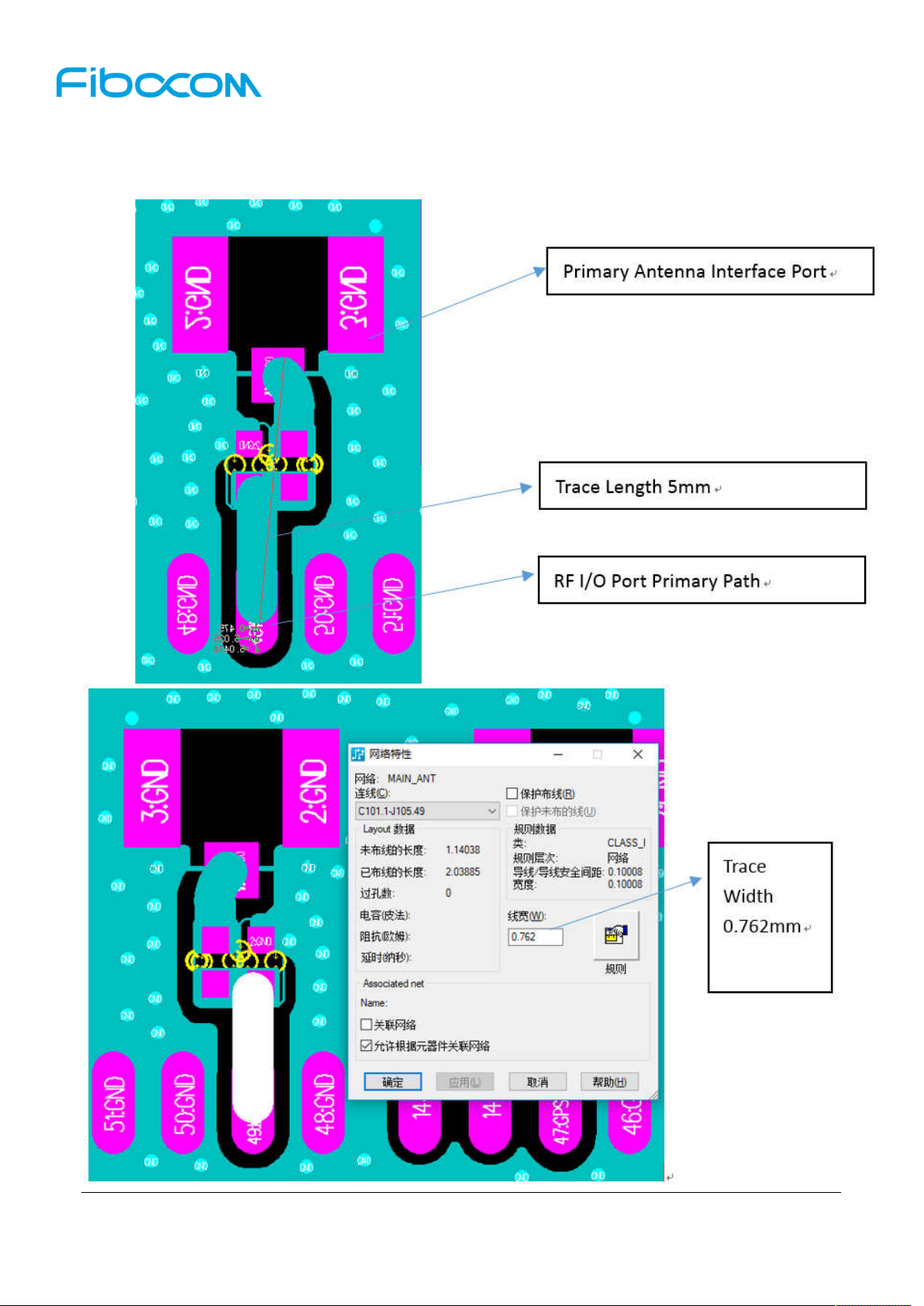
Appendix B ADP & MiniPCIe RF ports trace
1. NL668-AM MiniPCIe
a) Primary Antenna
Reproduction forbidden without Fibocom Wireless Inc. written authorization - All Rights Reserved.
FIBOCOM NL668-AM Hardware User Manual Page 57 of 62
Page 58
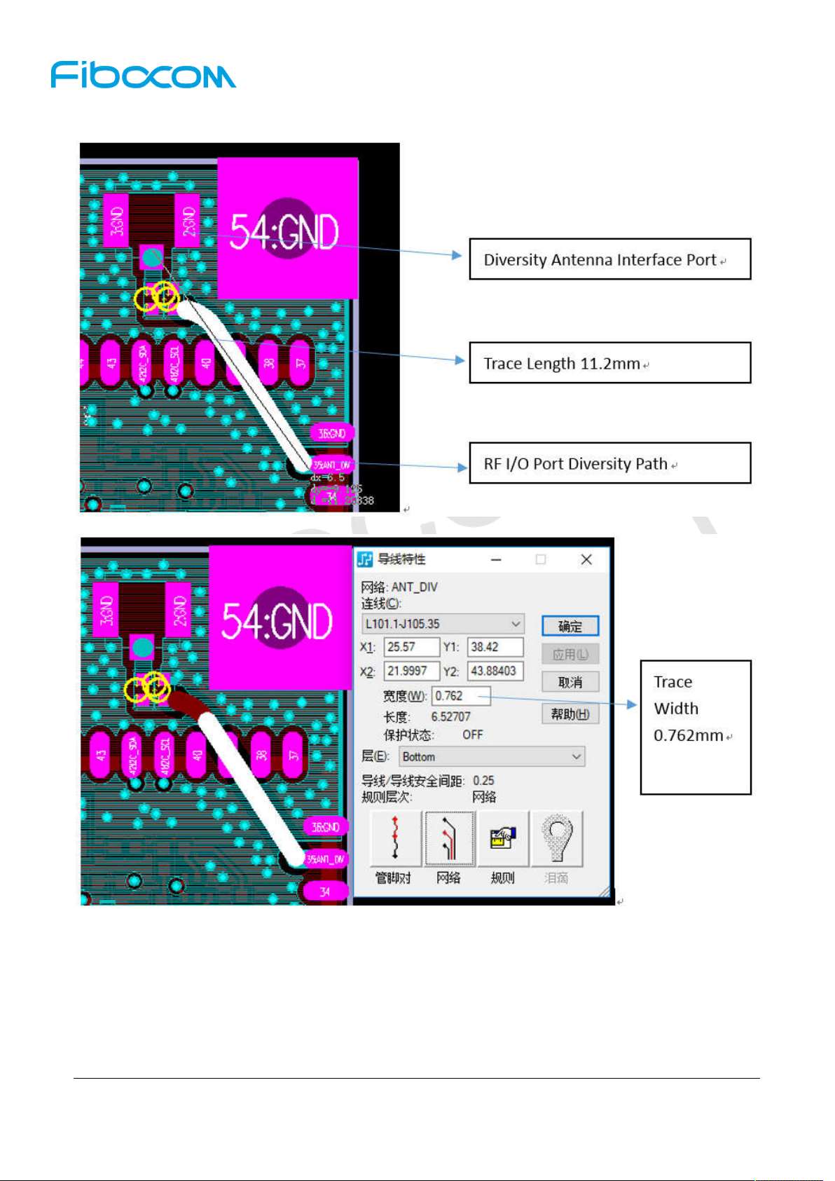
b) Diversity Antenna
Reproduction forbidden without Fibocom Wireless Inc. written authorization - All Rights Reserved.
FIBOCOM NL668-AM Hardware User Manual Page 58 of 62
Page 59
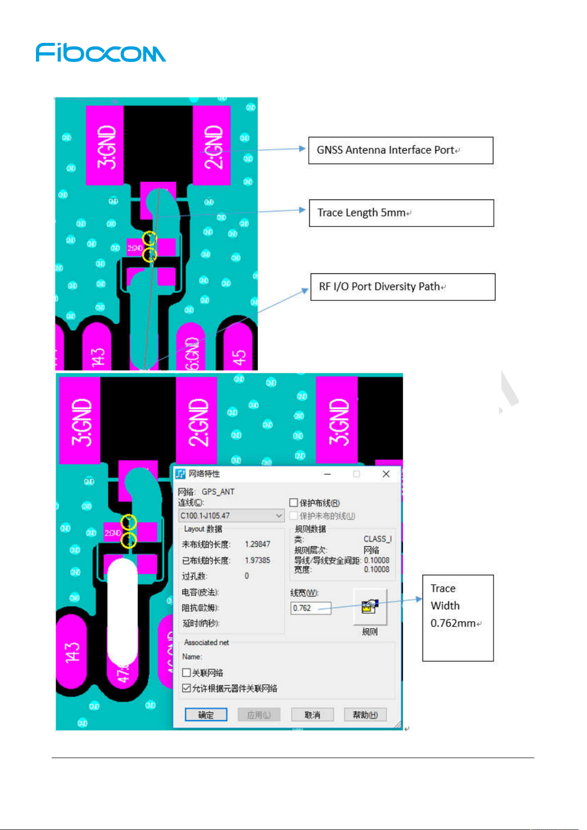
c) GNSS Antenna
Reproduction forbidden without Fibocom Wireless Inc. written authorization - All Rights Reserved.
FIBOCOM NL668-AM Hardware User Manual Page 59 of 62
Page 60
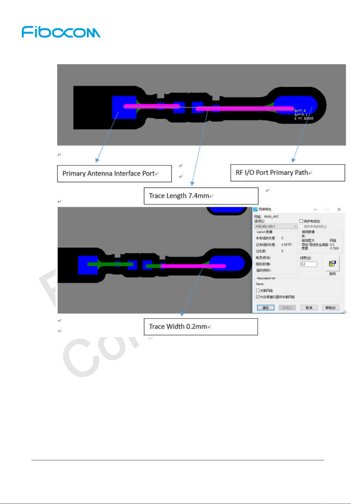
2. NL668-AM ADP
a) Primary Antenna
Reproduction forbidden without Fibocom Wireless Inc. written authorization - All Rights Reserved.
FIBOCOM NL668-AM Hardware User Manual Page 60 of 62
Page 61
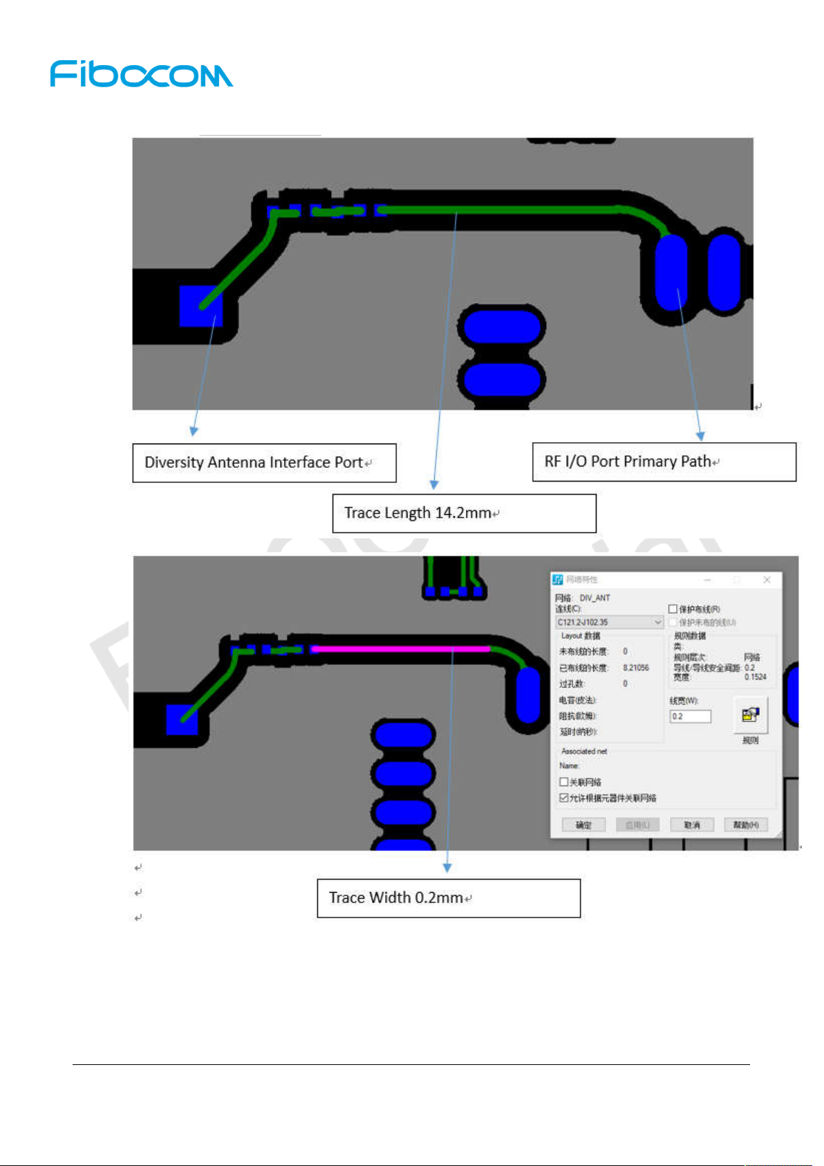
b) Diversity Antenna
Reproduction forbidden without Fibocom Wireless Inc. written authorization - All Rights Reserved.
FIBOCOM NL668-AM Hardware User Manual Page 61 of 62
Page 62
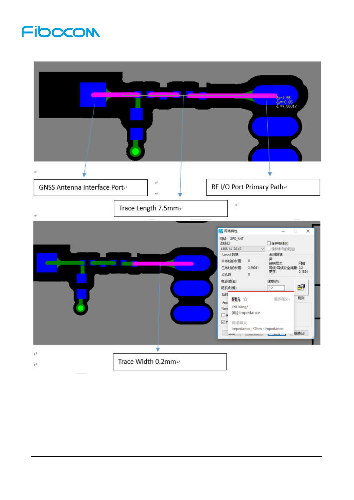
c) GNSS Antenna
Reproduction forbidden without Fibocom Wireless Inc. written authorization - All Rights Reserved.
FIBOCOM NL668-AM Hardware User Manual Page 62 of 62
 Loading...