

Fender SUPER CHAMP X2 COMBO, SUPER CHAMP X2 HEAD Service Manual
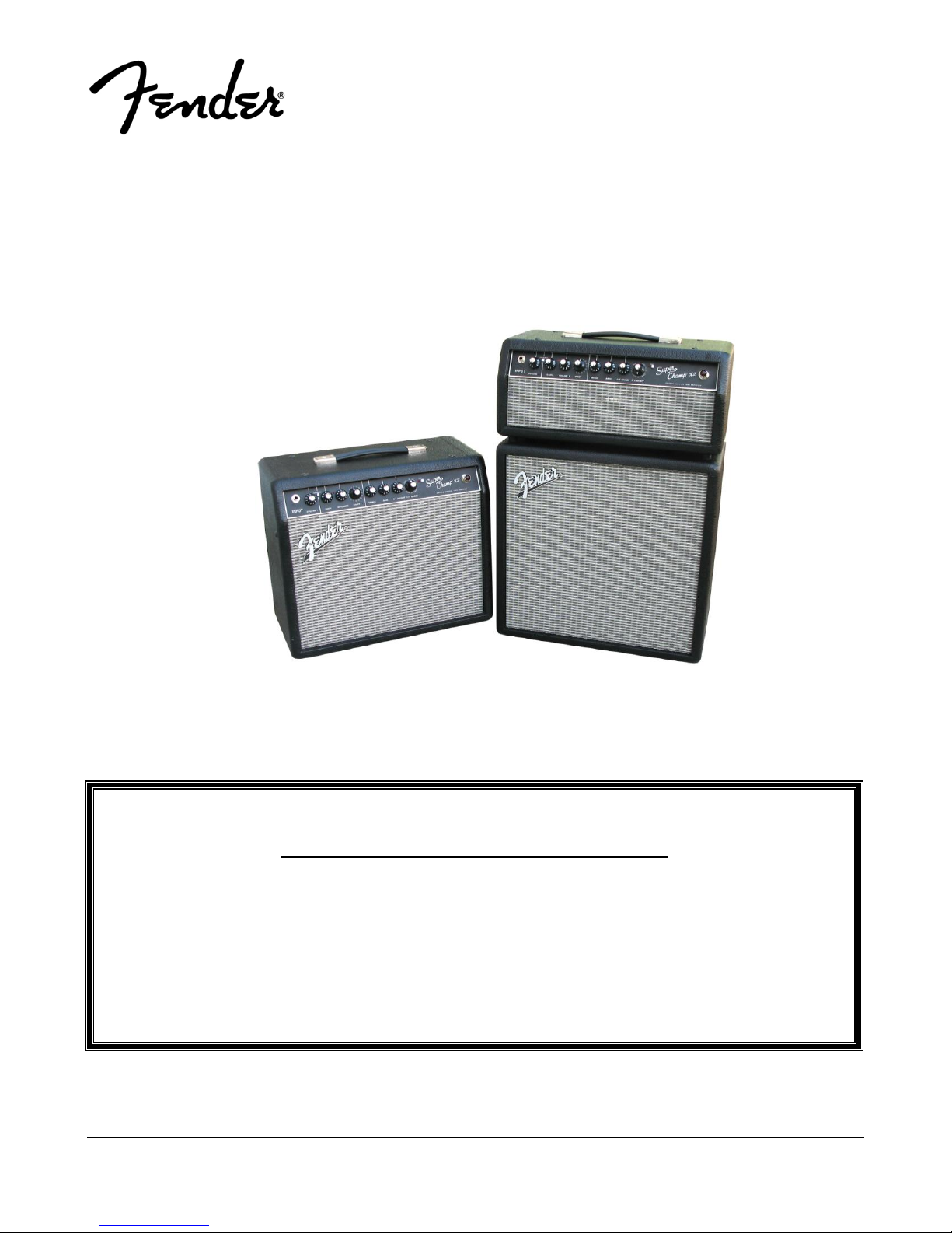
SUPER CHAMP X2 COMBO/ HEAD™
ATTENTION:
WARRANTY SERVICE PROCEDURES
The Super Champ X2 Combo and Head are considered to be field serviceable to the
component level. Except for the µDSP PCB which must be replaced as a complete
module. We do however understand that some circumstances may require replacement of
other PCB Assemblies. Any Fender Authorized Service Center in need of a warranty
replacement PCB Assembly for this unit should contact FMIC Tech Support by phone at
(866) 345-3642 or email: sevice@fender.com
(This is the model name for warranty claims)
COMBO p/n 2223000000 (120V)
HEAD p/n 2223100000 (120V)
SERVICE MANUAL
Fender Musical Instruments Corporation, 17600 North Perimeter Drive, Suite 100 Scottsdale, AZ 85255
Issued: March 2012
SUPER CHAMP X2 COMBO/HEAD™
2
(This is the model name for warranty claims)
IMPORTANT NOTICE
Copyright © 2012 FMIC. All rights reserved. All
information contained herein is CONFIDENTIAL
and PROPRIETARY and is the property of Fender® Musical Instruments Corporation. It is not to
be sold or assigned to another party and is disclosed solely for use by Fender Authorized
Service Centers for purposes of product service
and maintenance. All information is not to be disclosed to others without the expressed permission
of Fender® Musical Instruments Corporation. All
PARTS LIST CODES
The description codes used in the itemized Parts Lists are defined below:
CAPACITOR CODES
CAP AE = Aluminum Electrolytic
CAP CA = Ceramic Axial
CAP CD = Ceramic Disk
CAP CR = Ceramic Radial
CAP MPF = Metalized Polyester Film
CAP MY = Mylar
CAP PFF = Polyester Film/Foil
RESISTOR CODES
RES CC = Carbon Comp
RES CF = Carbon Film
RES FP = Flame Proof
RES MF = Metal Film
RES MOX = Metal Oxide
RES WW = Wire Wound
specifications are subject to change without notice. This information and any copies produced
electronically or otherwise must be surrendered
upon demand of Fender® Musical Instruments
Corporation.
Parts marked with two asterisks (**) indicate the
required use of that specific part. This is necessary for RELIABILITY and SAFETY requirements.
DO NOT USE A SUBSTITUTE!
HARDWARE CODES
BLX = Black Oxide
CR = Chrome Plated
HWH = Hex Washer Head
M = Machine Screw
NI = Nickel Plated
OHP = Oval Head Phillips
PB = Particle Board
PHP = Pan Head Phillips
PHPS = Pan Head Phillips Sems
SMA = Sheet Metal "A" Point
SMB = Sheet Metal "B" Point
SS = Stainless Steel
TF = Thread Forming
ZI = Zinc Plated

SUPER CHAMP X2 COMBO/HEAD™
3
(This is the model name for warranty claims)
SPECIFICATIONS
Model Name: SUPER CHAMP X2 COMBO/ HEAD
Release Number: PR 2259 PR 2260
HEAD COMBO
Part Numbers (120V, 60Hz) US: 2223000000 2223100000
(230V, 50Hz) EUR: 2223006900 2223106900
(230V, 50Hz) UK: 2223004900 2223104900
(240V, 50Hz) AUS: 2223003900 2223103900
(100V, 50Hz) JPN: 2223007900 2223007900
(220V, 50Hz) ROK: 2223009900 2223009900
(240V, 50Hz) ARG: 2223005900 2223005900
(110V, 50Hz) TW: 2223001900 2223001900
Power Requirement: 90 W
Power Output: 15 W RMS into 8 ohms @ 10 %THD
Power Amp Sensitivity: 10mV for 10 W into 8 ohms @ 5 %THD
Impedances Input (Pre-Amp): >1M Ohms
Effects Send: 1 kOhm
Effects Receive: 10 kOhm
Speaker Complement: Fender Special Design 8 ohm, 10”
(P/N 0091245000)
Footswitch 2 Button DC Footswitch Assy
(P/N 0071359000)
Dimensions Height: 15 in ( 38 cm)
Width: 17.5 in ( 45 cm)
Depth: 9 in ( 22.9 cm)
Weight: 24 lbs (10.9 kg)
Product specifications are subject to change without notice
SUPER CHAMP X2 COMBO/HEAD™
4
SERVICE NOTES
1. CHASSIS REMOVAL is accomplished by first
removing the COMBO or HEAD’s cabinet’s
back panel. Then remove the four (4) screws
from the top of the cabinet that secure the
chassis. Disconnect the ¼” speaker plug from
the speaker jack (COMBO only). Then slide the
chassis toward the rear of the cabinet.
2. MAIN PCB REMOVAL is accomplished by re-
moving the IEC Connector, the fuse holder, the
speaker jack nut, the line out jack nut and the
two screws that hold the chassis’ rear panel to
the chassis. Remove the rear panel and the vacuum tubes. Disconnect the ribbon cable that
goes between the main PCB and the uDSP
PCB. Remove all screws holding the main PCB
to the stand offs on the chassis. Then remove
the front panel knobs and the nuts holding the
(This is the model name for warranty claims)
controls to the front panel. Slide the front panel
PCB back away from the front panel. Remove
all the fast-ons connecting the main PCB to the
power indicator, the power transformer and the
output transformer. Now the main PCB can be
lifted up and out of the chassis taking advantage of the slots in the back of the chassis.
3. The COMBO and the HEAD share the same
chassis and circuitry. The combo contains a
captive 10” speaker while the head can be used
with any suitable speaker cabinet such as the
SC112 enclosure.
PCB EXCHANGE POLICY
Parts marked with a single asterisk (*) in the Part
Lists are not field replaceable. If a failure due to
one of these components is detected, please con-
CIRCUIT DESCRIPTION
This section provides concise information about
new or unusual circuitry designs incorporated into
this amplifier model. The purpose is to aid the service technician by providing insight into the design
areas most likely to become obstacles in troubleshooting. Information is focused for its effective use
while maintaining the security of Fender® proprietary information whenever possible.
MAIN PCB
The Main PCB Assy. contains the circuitry for the
pre-amplifier, the power amplifier, and the power
supply. The controls are located on a breakaway
tact the FMIC Customer Service Department to order the complete PCB Assembly.
section of the main PCB with ribbon cables connecting them.
PRE-AMPLIFIER
Op-amp U6-A provides the high impedance instrument input with 14db of gain. Op-amp U6-B is
configured as an active filter producing high frequency pre-emphasis. U1-A provides another 20db
of gain. Its’ output is clamped to +/-2V. The uDSP
PCB Assy. chooses either the low gain output from
U6-B or the higher gain output from U1-A depending on the amplitude of the guitar input signal. Opamp U3-A is configured as a differential input amp
recovering the signal after uDSP processing and
conversion back to an analog signal. The LOUT and

SUPER CHAMP X2 COMBO/HEAD™
5
ROUT signals are the input to the differential amp
which acts as a three pole active low pass filter for
de-emphasis. The output of U3-A is applied to a
buffer amp U1-A which drives op-amp U1-B which
provides the LINE OUT signal and the power amp
input. FET Q-1 provides system muting during
power up/down in conjunction with the power sense
circuits composed of D9, Q2, and Q4.
USER INTERFACE
The 4 – 16 position encoders (S2 – S3) for the
VOICE and EFFECT SELECT are sent to the GPIO
buss of the uDSP and polled at a 1000Hz rate.
The 6 potentiometers CH1 VOLUME (R85), CH2
VOLUME (R83), CH2 GAIN (R84), TREBLE (R82),
BASS (R81), and AND FX LEVEL (R80) generate
DC Voltages (0.0V to +3.3V) that are polled at a
1000Hz rate by the uDSP’s A/D converter.
POWER AMPLIFIER
The power amplifier consists of V1, V2, and V3. T2
and associated circuitry. The signal is fed to the
gate of V1-B in common cathode configuration. The
signal is then fed from the plate of V1-B to the gate
of V1-A which is operating as a phase splitter driving V2 from its’ plate and V3 from its’ cathode. V2
and V3 are operating in Class A-B push-pull mode.
T2 matches the impedance of V2’s plate to the 8
Ohm speaker. Negative feedback is provided by
R23 feeding signal back to V1-B’s cathode.
(This is the model name for warranty claims)
µDSP PCB
The µDSP PCB is located in the back of the chassis
opposite the power transformer. It provides the amplifier voicing and effects functions. The µDSP PCB
is not field serviceable and must be replaced as an
assembly.
USB PCB
The USB PCB provides the USB interface to the
µDSP and ESD protection. The USB interface is
used to communicate between the user’s computer
for the purpose of altering the amp’s presets or res-
toring the amp to factory settings.
POWER SUPPLY
T1 has four secondary windings for the +5V regulator, the +/-12V supplies, the tube filaments and the
high voltage supply. The violet winding is rectified
by a fullwave bridge, filtered by C41 and fed to the
µDSP PCB where it is regulated to +3.3VDC and
fed back on to the main PCB. Similarly, the center
tapped orange and yellow winding is rectified, filtered and fed to +/-12V zeners to provide power to
the operational amplifiers and other circuitry. The
red windings provide the high voltage for the vacuum tubes. The green winding provides 6.3VAC
for the vacuum tube filaments. A voltage doubler is
employed to produce -41.9VDC to bias the output
tubes, V2 and V3.
.
 Loading...