Fairchild Semiconductor SSTV16859 Datasheet

SSTV16859
Dual Output 13-Bit Register with
SSTL-2 Compatible I/O and Reset
SSTV16859 Dual Output 13-Bit Register with SSTL-2 Compatible I/O and Reset
March 2001
Revised July 2002
General Description
The SSTV16859 i s a dual output 13-bit register designed
for use with 184 and 232 pin DDR-1 memory modules. The
device has a differential input clock, SSTL-2 compatible
data inputs and a LVCMOS compatible RE SET
device has been designed to meet the JEDEC DDR module register specifications.
The device has been fabricated on an advanced submicron CMOS process and is designed to operate at power
supplies of less than 3.6V’s.
input. The
Features
■ Compliant with DDR-I registered module specifications
■ Operates at 2.5V
■ SSTL-2 compatible input structure
■ SSTL-2 compliant output structure
■ Differential SSTL-2 compatible clock inputs
■ Low power mode when device is reset
■ Industry standard 64 pin TSSOP package
■ Also packaged in plastic Fine-Pitch Ball Grid Array
(FBGA)
± 0.2V V
Ordering Code:
Order Number Package Number Package Description
SSTV16859G
(Note 1)(Note 2)
SSTV16859MTD
(Note 2)
Note 1: Ordering code “G” indicates Trays.
Note 2: Devices also available in Tape and Reel. Specify by appending th e s uffix let t er “X” to the ordering code.
BGA96A 96-Ball Fine-Pitch Ball Grid Array (FBGA), JEDEC MO-205, 5.5mm Wide
MTD64 64-Lead Thin Shrink Small Outline Package (TSSOP), JEDEC MO-153, 6.1mm Wide
DD
© 2002 Fairchild Semiconductor Corporation DS500414 www.fairchildsemi.com

Connection Diagrams
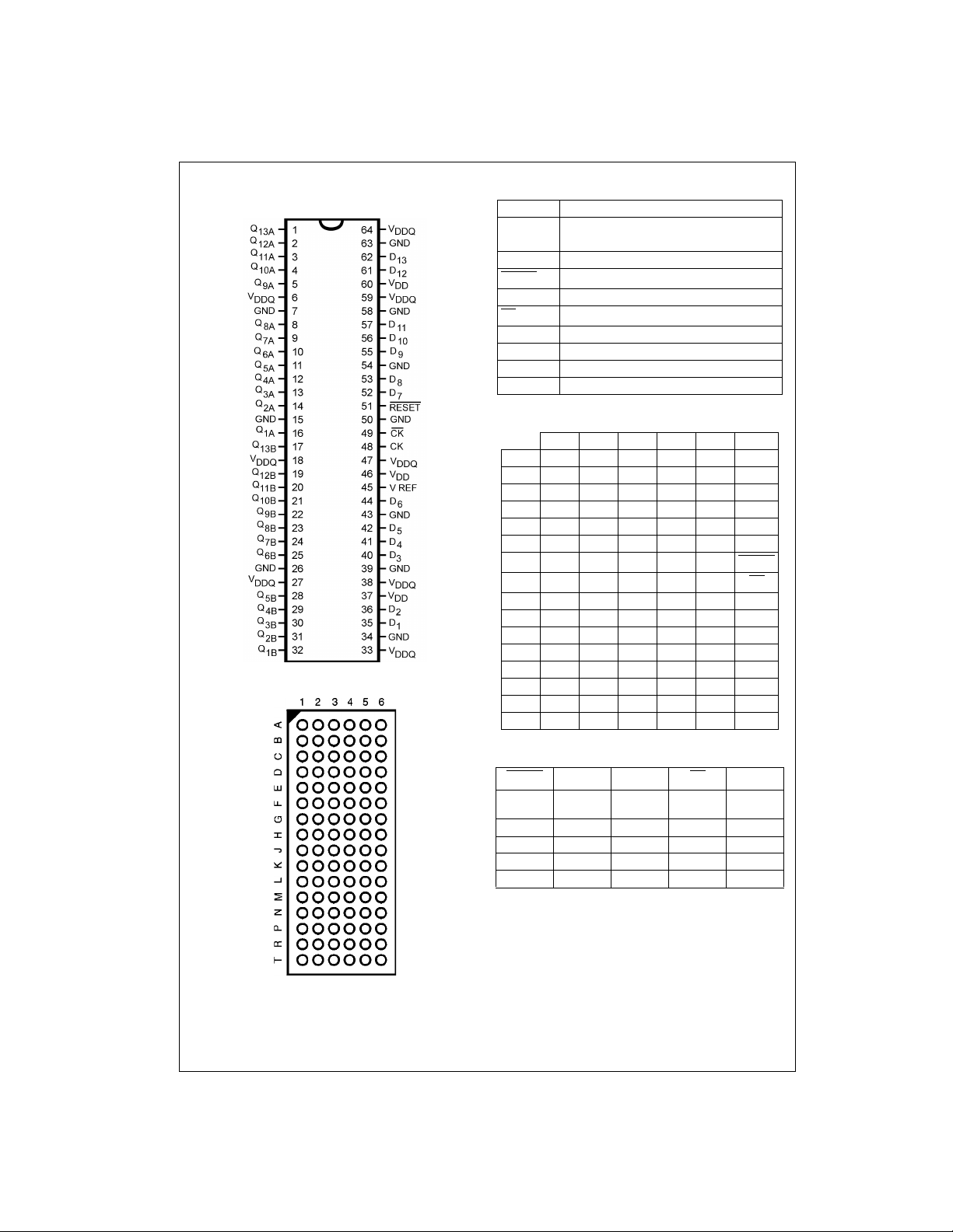
Pin Assignment for TSSOP
SSTV16859
Pin Assignment for FBGA
Pin Descriptions
Pin Name Description
Q
1A-Q13A
Q
1B-Q13B
D1-D
RESET
SSTL-2 Compatible Register Outputs
SSTL-2 Compatible Register Inputs
13
Asynchronous LVCMOS Reset Input
CK Positive Master Clock Input
CK
V
V
V
REF
DDQ
DD
Negative Master Clock Input
Voltage Reference Pin for SSTL level inputs
Power Supply Voltage for Output Signals
Power Supply Voltage for Inputs
NC Electrically Isolated No Connect
FBGA Pin Assignments
12345 6
A NC NC NC NC NC NC
B Q
12AQ13A
C Q
10AQ11A
D Q
8AQ9AVDDQVDDQD13
E Q6AQ7AV
F Q4AQ5AV
G Q2AQ3AGND GND D7RESET
H Q1AQ
J Q
12BQ11B
K Q
10BQ9BVDDQVDD
L Q
8BQ7BVDDQVDDD5
M Q6BQ5BV
N Q4BQ3BGND GND D
P Q2BQ1BGND GND NC NC
R NC NC NC NC NC NC
T NC NC NC NC NC NC
GND GND NC NC
GND GND NC NC
DDQVDDD11
DDQVDDD9
GND GND NC CK
13B
GND V
REF
DDQVDDQD3
NC CK
NC NC
D
12
D
10
D
8
D
6
D
4
D
1
2
(Top Thru View)
www.fairchildsemi.com 2
Truth Table
RESET
L
HL
HH
HXLHQ
HXHLQ
L = Logic LOW
H = Logic HIGH
X = Don’t Care but not floating unless noted
↑ = LOW-to-HIGH Clock Transition
↓ = HIGH-to-LOW Clock Transition
= Output Remains in Previously Clocked State
Q
n-1
D
n
X or
Floating
CK CK
X or
Floating
X or
Floating
↑↓L
↑↓H
Q
n
L
n-1
n-1

Functional Description
The SSTV16859 is a 13-bit dual register with SSTL-2 compatible inputs and outputs. Input da ta is transferr ed to output data on the rising edge o f the differential clock pair.
When the RESET
placed into the LOW logic state an d all input comparato rs
are disabled for powe r savings. Output glitches are prevented by disabling the internal re giste rs mor e quickly than
the input comparators. When RESET
tem designer must insu re the cloc k and data inp uts to the
signal is asserted LOW all outp uts are
is removed, the sys-
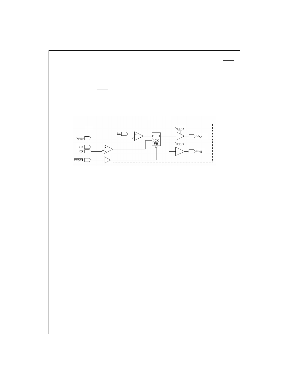
Logic Diagram
For n = 1 to 13
device are stable during the ri sing transiti on of the RESET
signal.
The SSTL-2 data inputs trans ition based on the value of
V
. V
REF
the trip point of the input buffers of the SSTV16859 and
other SSTL-2 compatible devices.
The RESET
and is not referenced to the V
is a stable system reference used for setting
REF
signal is a standard CMOS compatible inpu t
REF
signal.
SSTV16859
3 www.fairchildsemi.com
 Loading...