Fairchild Semiconductor SSTV16857 Datasheet

September 2000
Revised February 2001
SSTV16857
14-Bit Register with SSTL-2 Compatible I/O and Reset
SSTV16857 14-Bit Register with SSTL-2 Compatible I/O and Reset
General Description
The SSTV16857 is a 14-b it register designed for use with
184 and 232 pin DDR-I memory modules. The device has
a differential input clock, SSTL-2 compatible data inputs
and a LVCMOS compatible RESET
been designed for compliance with the JEDEC DDR module and register specifications.
The device is fabricated on an advanced submicron CMOS
process and is designed to op erate at power supplies of
less than 3.6V’s.
input. The device has
Features
■ Compliant with DDR-I registered module specifications
■ Operates at 2.5V
■ SSTL-2 compatible input and output structure
■ Differential SSTL-2 compatible clock inputs
■ Low power mode when device is reset
■ Industry standard 48 pin TSSOP package
± 0.2V V
DD
Ordering Code:
Order Number Package Number Package Description
SSTV16857MTD MTD48 48-Lead Thin Shrink Small Outline Package (TSSOP), JEDEC MO-153, 6.1mm Wide
Devices also availab l e in Tape and Reel. Specify by appending th e s uffix let t er “X” to the ordering code.
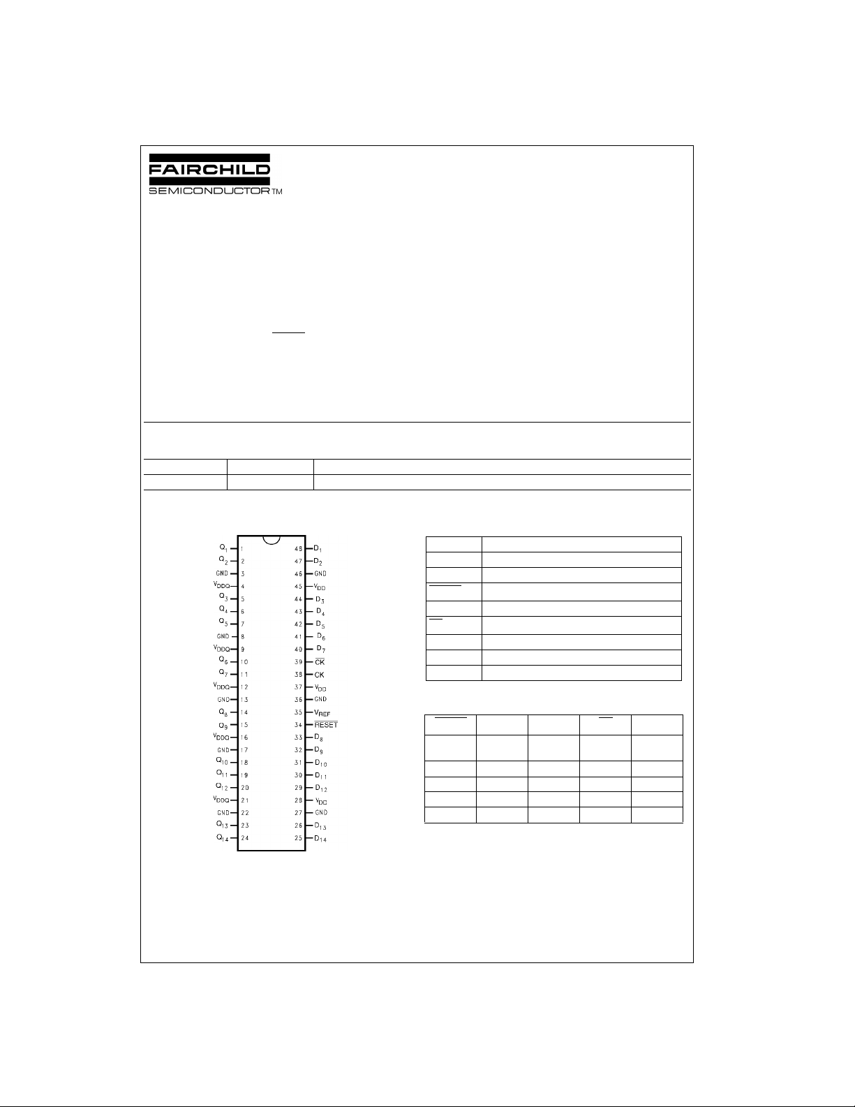
Connection Diagram Pin Descriptions
Pin Name Description
Q
1-Q14
D
1-D14
RESET
CK Positive Master Clock Input
CK
V
REF
V
DDQ
V
DD
SSTL-2 Compatible Output
SSTL-2 Compatible Inputs
Asynchronous LVCMOS Reset Input
Negative Master Clock Input
Voltage Reference Pin for SSTL Level Inputs
Power Supply Voltage for Output Signals
Power Supply Voltage for Inputs
Truth Table
RESET
LX or
HL
HH
HXLHQ
HXHLQ
L = Logic LOW
H = Logic HIGH
X = Don’t Care, but not floating unless noted
↑ = LOW-to-HIGH Clock Transition
↓ = HIGH-to-LOW Clock Transition
© 2001 Fairchild Semiconductor Corporation DS500387 www.fairchildsemi.com
D
n
Floating
CK CK
X or
Floating
↑↓L
↑↓H
X or
Floating
Q
n
L
n
n

Functional Description
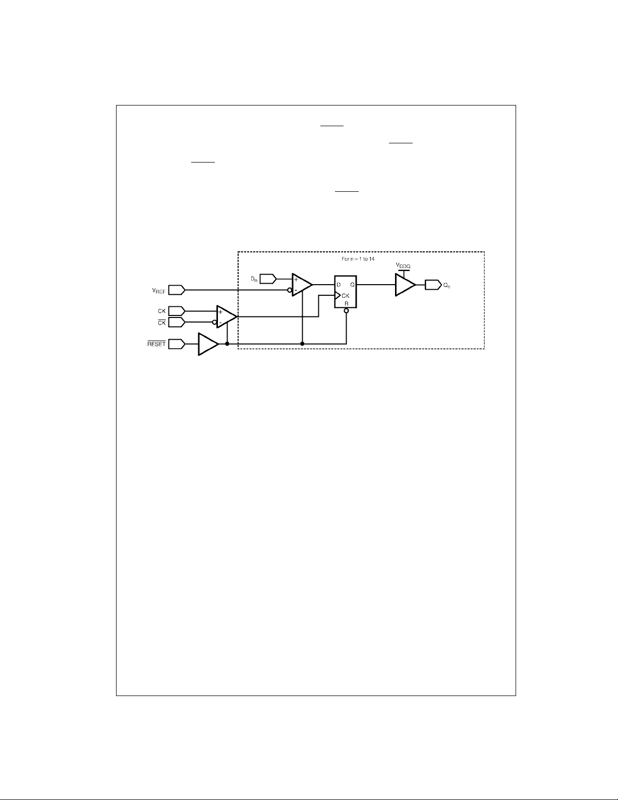
The SSTV16857 is a 14-b it register with SSTL-2 compatible inputs and outputs. Input data is captured by the register on the positive edge cros sing of the differential clock
pair.
SSTV16857
When the LV-CMOS RESET
outputs and internal reg isters are asynchronously placed
into the LOW logic state. In addition, the clock and data differential comparator s are disabl ed for power savings. Output glitches are prevented by disabling the internal
registers more qui ckly than the input comparat ors. When
signal is asserted LOW, all
Logic Diagram
RESET
is removed, the system designer must insure the
clock and data inputs to th e device are stable during the
rising transition of the RESET
The SSTL-2 data inputs tr ansition based on the value of
V
. V
REF
the trip point of the input buffers of the SSTV16857 and
other SSTL-2 compatible devices.
The RESET
and is not referenced to the V
is a stable system reference used for setting
REF
signal is a standar d CMOS compatible in put
signal.
signal.
REF
www.fairchildsemi.com 2
 Loading...