

Fairchild Semiconductor SSP7N60B, SSS7N60B Datasheet
SSP7N60B/SSS7N60B
600V N-Channel MOSFET
SSP7N60B/SSS7N60B
General Description
These N-Channel enhancement mode power field effect
transistors are produced using Fairchild’s proprietary,
planar, DMOS technology.
This advanced technology has been especially tailored to
minimize on-state resistance, provide superior switching
performance, and withstand high energy pulse in the
avalanche and commutation mode. These devices are well
suited for high efficiency switch mode power supplies.
Features
• 7.0A, 600V, R
• Low gate charge ( typical 38 nC)
• Low Crss ( typical 23 pF)
• Fast switching
• 100% avalanche tested
• Improved dv/dt capability
• TO-220F package isolation = 4.0kV
= 1.2Ω @VGS = 10 V
DS(on)
(Note 6)
D
G
G
D
S
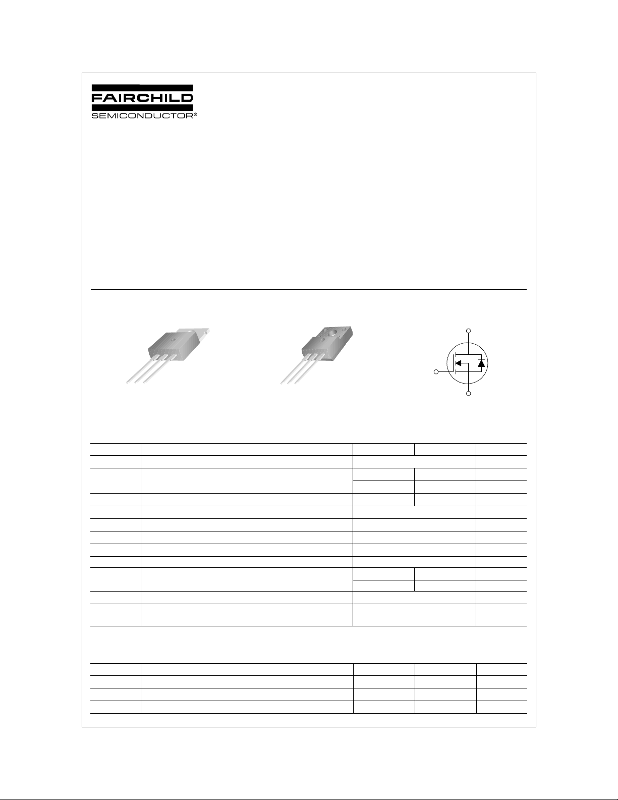
TO-220
SSP Series
D
G
S
TO-220F
SSS Series
S
Absolute Maximum Ratings T
= 25°C unless otherwise noted
C
Symbol Parameter SSP7N60B SSS7N60B Units
V
DSS
I
D
I
DM
V
GSS
E
AS
I
AR
E
AR
dv/dt Peak Diode Recovery dv/dt
P
D
Drain-Source Voltage 600 V
Drain Current
- Continuous (T
- Continuous (T
Drain Current - Pulsed
= 25°C)
C
= 100°C)
C
(Note 1)
7.0 7.0 * A
4.4 4.4 * A
28 28 * A
Gate-Source Voltage ± 30 V
Single Pulsed Avalanche Energy
Avalanche Current
Repetitive Avalanche Energy
Power Dissipation (TC = 25°C)
(Note 2)
(Note 1)
(Note 1)
(Note 3)
420 mJ
7.0 A
14.7 mJ
5.5 V/ns
147 48 W
- Derate above 25°C 1.18 0.38 W/°C
T
, T
J
STG
T
L
* Drain current limited by maximum junction temperature
Operating and Storage Temperature Range -55 to +150 °C
Maximum lead temperature for soldering purposes,
1/8" from case for 5 seconds
300 °C
Thermal Characteristics
Symbol Parameter SSP7N60B SSS7N60B U nits
R
θJC
R
θCS
R
θJA
©2002 Fairchild Semiconductor Corporation Rev. B, June 2002
Thermal Resistance, Junction-to-Case Max. 0.85 2.6 °C/W
Thermal Resistance, Case-to-Sink Typ. 0.5 -- °C/W
Thermal Resistance, Junction-to-Ambient Max. 62.5 62.5 °C/W
SSP7N60B/SSS7N60B
Electrical Characteristics T
= 25°C unless otherwise noted
C
Symbol Parameter Test Conditions Min Typ Max Units
Off Characteristics
BV
DSS
∆BV
DSS
/ ∆T
I
DSS
I
GSSF
I
GSSR
Drain-Source Breakdown Voltage
Breakdown Voltage Temperature
Coefficient
J
Zero Gate Voltage Drain Current
Gate-Body Leakage Current, Forward
Gate-Body Leakage Current, Reverse
= 0 V, ID = 250 µA
V
GS
I
= 250 µA, Referenced to 25°C
D
V
= 600 V, VGS = 0 V
DS
V
= 480 V, TC = 125°C
DS
V
= 30 V, VDS = 0 V
GS
= -30 V, VDS = 0 V
V
GS
600 -- -- V
-- 0.65 -- V/°C
-- -- 10 µA
-- -- 100 µA
-- -- 100 nA
-- -- -100 nA
On Characteristics
V
R
g
FS
GS(th)
DS(on)
Gate Threshold Voltage
Static Drain-Source
On-Resistance
Forward Transconductance
V
= VGS, ID = 250 µA
DS
= 10 V, ID = 3.5 A
V
GS
= 40 V, ID = 3.5 A
V
DS
(Note 4)
2.0 -- 4.0 V
-- 1.0 1.2 Ω
-- 8.2 -- S
Dynamic Characteristics
C
iss
C
oss
C
rss
Input Capacitance
Output Capacitance -- 115 150 pF
Reverse Transfer Capacitance -- 23 30 pF
= 25 V, VGS = 0 V,
V
DS
f = 1.0 MHz
-- 1380 1800 pF
Switching Characteristics
t
d(on)
t
r
t
d(off)
t
f
Q
Q
Q
g
gs
gd
Turn-On Delay Time
Turn-On Rise Time -- 80 170 ns
Turn-Off Delay Time -- 125 260 ns
Turn-Off Fall Time -- 85 180 ns
Total Gate Charge
Gate-Source Charge -- 6.4 -- nC
Gate-Drain Charge -- 15 -- nC
= 300 V, ID = 7.0 A,
V
DD
= 25 Ω
R
G
V
= 480 V, ID = 7.0 A,
DS
V
GS
= 10 V
(Note 4, 5)
(Note 4, 5)
-- 30 70 ns
-- 38 50 nC
Drain-Source Diode Characteristics and Maximum Ratings
I
S
I
SM
V
SD
t
rr
Q
rr
Notes:
1. Repetitive Rating : Pulse width limited by maximum junction temperature
2. L = 15.7mH, IAS = 7.0A, VDD = 50V, RG = 25 Ω, Starting TJ = 25°C
3. ISD ≤ 7.0A, di/dt ≤ 300A/µs, VDD ≤ BV
4. Pulse Test : Pulse width ≤ 300µs, Duty cycle ≤ 2%
5. Essentially independent of operating temperature
6. Only for back side in V
©2002 Fairchild Semiconductor Corporation
Maximum Continuous Drain-Source Diode Forward Current -- -- 7.0 A
Maximum Pulsed Drain-Source Diode Forward Current -- -- 28 A
= 0 V, IS = 7.0 A
Drain-Source Diode Forward Voltage
Reverse Recovery Time
Reverse Recovery Charge -- 4. 6 -- µC
Starting TJ = 25°C
DSS,
= 4.0kV and t = 0.3s
iso
V
GS
= 0 V, IS = 7.0 A,
V
GS
/ dt = 100 A/µs
dI
F
-- -- 1.4 V
-- 415 -- ns
(Note 4)
Rev. B, June 2002
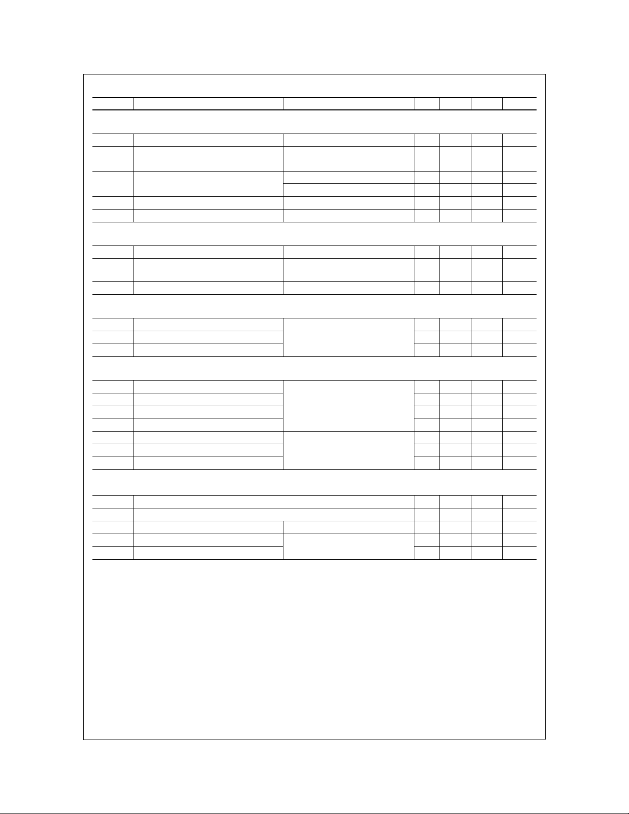
Typical Characteristics
SSP7N60B/SSS7N60B
V
GS
Top : 1 5 .0 V
10.0 V
1
8.0 V
10
7.0 V
6.5 V
6.0 V
5.5 V
Botto m : 5.0 V
0
10
, Drain Current [A]
D
I
-1
10
-1
10
0
10
!
Note s :
1. 25 0#s Pulse Test
2. T
= 25
C
1
10
VDS, Drain-Source Voltage [V]
5
4
],
3
$
[
DS(ON)
2
R
1
Drain-Source On-Resistance
0
0 5 10 15 20 25
VGS = 10V
VGS = 20V
!
Note : T
ID, Drain Current [A]
1
10
"
150oC
0
10
25oC
, Drain Current [A]
D
I
-1
10
246810
-55oC
!
Note s :
= 40V
1. V
DS
2. 25 0#s Pulse Test
VGS, Gate-Source Voltage [V]
Figure 2. Transfer CharacteristicsFigure 1. On-Region Char act er i stic s
1
10
"
= 25
J
0
10
"
, Reverse Drain Current [A]
DR
I
-1
10
0.2 0.4 0.6 0.8 1.0 1.2 1.4
150
"
25
!
Note s :
= 0V
1. V
GS
2. 25 0#s Pulse Test
VSD, Source-Drain voltage [V]
Figure 3. On-Resistance Variation vs
Drain Current and Gate Voltage
Figure 4. Body Diode Forward Voltage
Variation with Source Current
and Temperature
3000
2500
2000
1500
1000
Capacitance [pF]
500
0
-1
10
VDS, Drain-Source Voltage [V]
C
= Cgs + Cgd (Cds = shorted)
iss
C
= Cds + C
oss
gd
C
= C
rss
gd
C
iss
C
oss
C
rss
0
10
10
!
1. V
2. f = 1 MHz
1
Note s :
= 0 V
GS
12
10
8
6
4
, Gate-Source Voltage [V]
GS
2
V
0
0 5 10 15 20 25 30 35 40
QG, Tota l G a te C h a rg e [n C ]
VDS = 120V
VDS = 300V
VDS = 480V
!
Note : I
= 7.0 A
D
Figure 5. Capacitance Characteristics Figure 6. Gate Charge C haracteristics
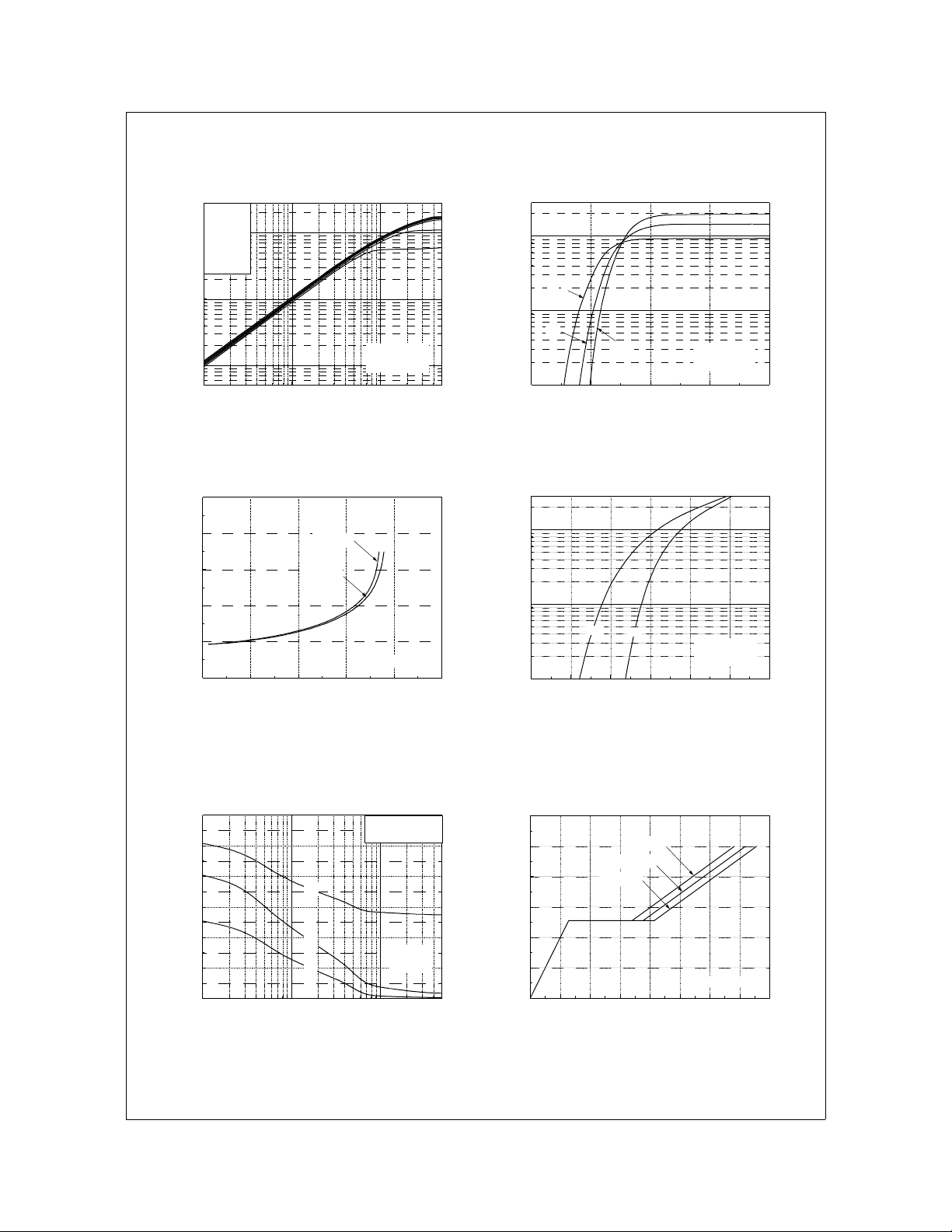
©2002 Fairchild Semiconductor Corporation Rev. B, June 2002
Typical Characteristics (Continued)
SSP7N60B/SSS7N60B
1.2
1.1
1.0
, (Normalized)
DSS
BV
0.9
Drain-Source Breakdown Voltage
0.8
-100 -50 0 50 100 150 200
!
1. V
2. I
Note s :
= 0 V
GS
= 250 #A
D
TJ, Junction Temperature [oC]
Figure 7. Breakdown Voltage Variation
vs Temperature
2
10
1
10
0
10
, Drain Current [A]
D
I
-1
10
-2
10
0
10
Operation in This Area
is Limited by R
DS(on)
10 ms
DC
!
Note s :
1. T
= 25 oC
C
2. T
= 150 oC
J
3. Single Pulse
1
10
2
10
VDS, Drain-Source Voltage [V]
1 ms
100 µs
10 µs
3.0
2.5
2.0
1.5
, (Normalized)
1.0
DS(ON)
R
Drain-Source On-Resistance
0.5
0.0
-100 -50 0 50 100 150 200
!
Note s :
1. V
= 10 V
GS
= 3.5 A
2. I
D
TJ, Junction Temperature [oC]
Figure 8. On-Resistance Variation
2
10
1
10
0
3
10
10
, Drain Current [A]
D
-1
I
10
-2
10
0
10
Operation in This Area
is Limited by R
DS(on)
1 ms
10 ms
100 ms
DC
!
Note s :
1. T
= 25 oC
C
2. T
= 150 oC
J
3. Single Pulse
1
10
2
10
VDS, Drain-Source Voltage [V]
100 µs
3
10
Figure 9-1. Maximum Safe O per at in g Are a
for SSP7N60B
8
6
4
, Drain Current [A]
D
I
2
0
25 50 75 100 125 150
Figure 9-2. Maximum Safe Operating Area
for SSS7N60B
TC, Case Tem pera ture ["]
Figure 10. Maximum Drain Current
vs Case Temperature
©2002 Fairchild Semiconductor Corporation Rev. B, June 2002
 Loading...