

Fairchild Semiconductor SSS1N50B Datasheet

©2002 Fairchild Semiconductor Corporation Rev. B, May 2002
SSP1N50B
SSP1N50B
520V N-Channel M OSFET
General Description
These N-Channel enhancement mode power field effect
transistors are produced using Fairchild’s proprietary,
planar, DMOS technology.
This advanced technology has been especially tailored to
minimize on-state resistance, provide superior switching
performance, and withstand high energy pulse in the
avalanche and commutation mode. These devices are well
suited for high efficiency switch mode power supplies,
power factor correction and electronic lamp ballasts based
on half bridge.
Features
• 1.5A, 520V, R
DS(on)
= 5.3Ω @VGS = 10 V
• Low gate charge ( typical 8.3 nC)
• Low Crss ( typical 5.5 pF)
• Fast switching
• 100% avalanche tested
• Improved dv/dt capability
Absolute Maximum Ratings T
C
= 25°C unless otherwise noted
Thermal Characteristics
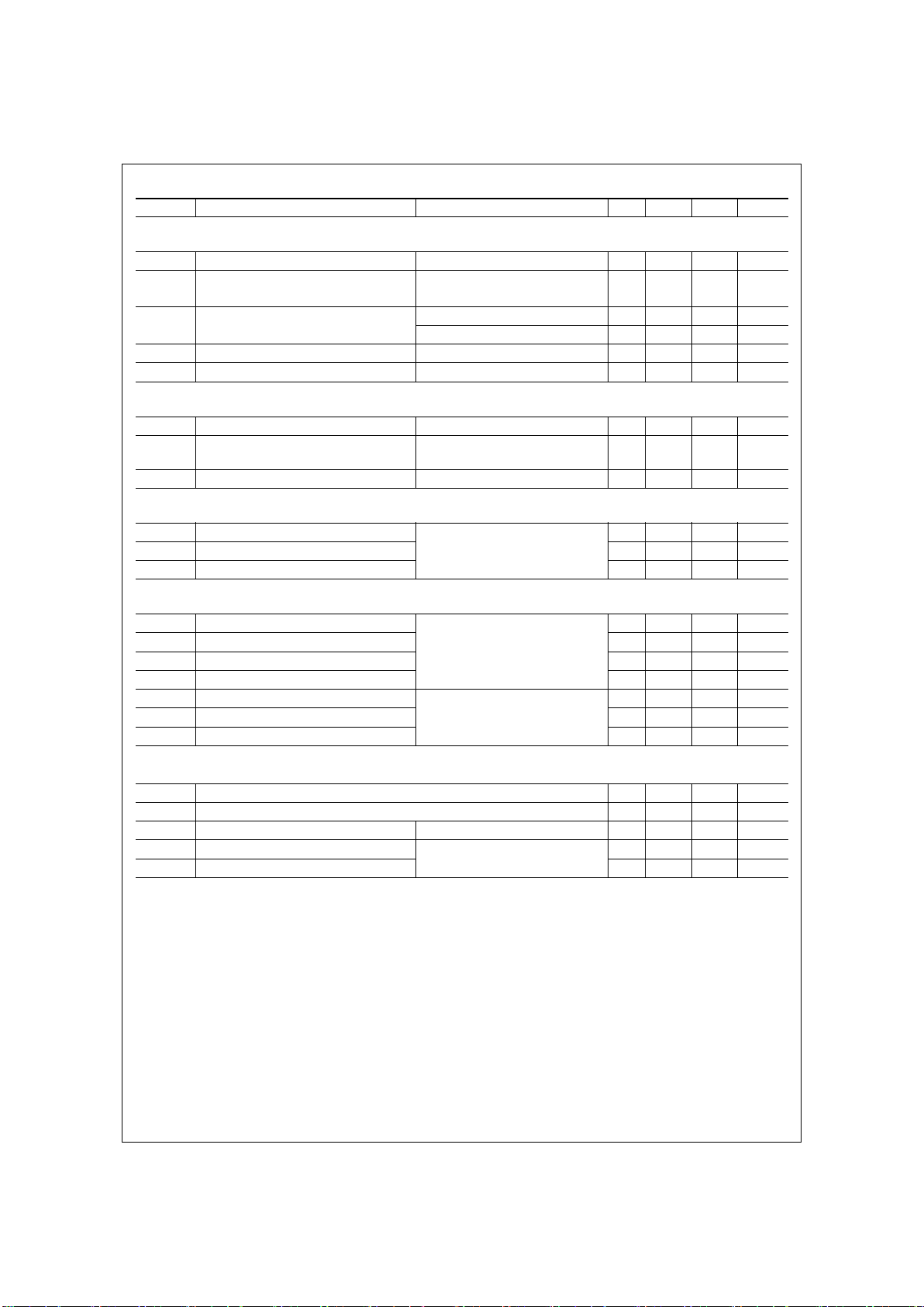
Symbol Parameter SSP1N50B Units
V
DSS
Drain-Source Voltage 520 V
I
D
Drain Current
- Continuous (T
C
= 25°C)
1.5 A
- Continuous (T
C
= 100°C)
0.97 A
I
DM
Drain Current - Pulsed
(Note 1)
5.0 A
V
GSS
Gate-Source Voltage ± 30 V
E
AS
Single Pulsed Avalanche Energy
(Note 2)
100 mJ
I
AR
Avalanche Current
(Note 1)
1.5 A
E
AR
Repetitive Avalanche Energy
(Note 1)
3.6 mJ
dv/dt Peak Diode Recovery dv/dt
(Note 3)
3.5 V/ns
P
D
Power Dissipation (TC = 25°C)
36 W
- Derate above 25°C 0.29 W/°C
T
J
, T
STG
Operating and Storage Temperature Range -55 to +150 °C
T
L
Maximum lead temperature for soldering purposes,
1/8" from case for 5 seconds
300 °C
Symbol Parameter Typ Max Units
R
θJC
Thermal Resistance, Junction-to-Case -- 3.44 °C/W
R
θCS
Thermal Resistance, Case-to-Sink 0.5 -- °C/W
R
θJA
Thermal Resistance, Junction-to-Ambient -- 62.5 °C/W
TO-220
SSP Series
G
S
D
!!!!
!!!!
!!!!
""""
!!!!
!!!!
!!!!
####
!!!!
!!!!
!!!!
""""
!!!!
!!!!
!!!!
####
S
D
G
Rev. B, May 2002
SSP1N50B
©2002 Fairchild Semiconductor Corporation
Electrical Characteristics T
C
= 25°C unless otherwise noted
Notes:
1. Repetitive Rating : Pulse width limited by maximum junction temperature
2. L = 80mH, IAS = 1.5A, VDD = 50V, RG = 25 Ω, Starting TJ = 25°C
3. ISD ≤ 1.5A, di/dt ≤ 200A/µs, VDD ≤ BV
DSS,
Starting TJ = 25°C
4. Pulse Test : Pulse width ≤ 300µs, Duty cycle ≤ 2%
5. Essentially independent of operating temperature
Symbol Parameter Te st Conditions Min Typ Max Units
Off Characteristics
BV
DSS
Drain-Source Breakdown Voltage
V
GS
= 0 V, ID = 250 µA
520 -- -- V
∆BV
DSS
/ ∆T
J
Breakdown Voltage Temperature
Coefficient
I
D
= 250 µA, Referenced to 25°C
-- 0.54 -- V/°C
I
DSS
Zero Gate Voltage Drain Current
V
DS
= 520 V, VGS = 0 V
-- -- 10 µA
V
DS
= 400 V, TC = 125°C
-- -- 100 µA
I
GSSF
Gate-Body Leakage Current, Forward
V
GS
= 30 V, VDS = 0 V
-- -- 100 nA
I
GSSR
Gate-Body Leakage Current, Reverse
V
GS
= -30 V, VDS = 0 V
-- -- -100 nA
On Characteristics
V
GS(th)
Gate Threshold Voltage
V
DS
= VGS, ID = 250 µA
2.0 -- 4.0 V
R
DS(on)
Static Drain-Source
On-Resistance
V
GS
= 10 V, ID = 0.75 A
-- 4.1 5.3 Ω
g
FS
Forward Transconductance
V
DS
= 40 V, ID = 0.75 A
-- 1.8 -- S
Dynamic Characteristics
C
iss
Input Capacitance
V
DS
= 25 V, VGS = 0 V,
f = 1.0 MHz
-- 260 340 pF
C
oss
Output Capacitance -- 25 33 pF
C
rss
Reverse Transfer Capacitance -- 5.5 7.2 pF
Switching Characteristics
t
d(on)
Turn-On Delay Time
V
DD
= 250 V, ID = 1.5 A,
R
G
= 25 Ω
-- 14 40 ns
t
r
Turn-On Rise Time -- 40 90 ns
t
d(off)
Turn-Off Delay Time -- 35 80 ns
t
f
Turn-Off Fall Time -- 35 80 ns
Q
g
Total Gate Charge
V
DS
= 400 V, ID = 1.5 A,
V
GS
= 10 V
-- 8.3 11 nC
Q
gs
Gate-Source Charge -- 1.5 -- nC
Q
gd
Gate-Drain Charge -- 3.4 -- nC
Drain-Source Diode Characteristics and Maximum Ratings
I
S
Maximum Continuous Drain-Source Diode Forward Current -- -- 1.5 A
I
SM
Maximum Pulsed Drain-Source Diode Forward Current -- -- 5.0 A
V
SD
Drain-Source Diode Forward Voltage
V
GS
= 0 V, IS = 1.5 A
-- -- 1.4 V
t
rr
Reverse Recovery Time
V
GS
= 0 V, IS = 1.5 A,
dI
F
/ dt = 100 A/µs
-- 230 -- ns
Q
rr
Reverse Recovery Charge -- 0.94 -- µC

Rev. B, May 2002
SSP1N50B
©2002 Fairchild Semiconductor Corporation
0.2 0.4 0.6 0.8 1.0 1.2 1.4
10
-1
10
0
150
$
%
Note s :
1. V
GS
= 0V
2. 250&s Pulse Test
25
$
I
DR
, Reverse Drain Current [A]
VSD, Source-Drain voltage [V]
012345
3
6
9
12
15
VGS = 20V
VGS = 10V
%
Note : T
J
= 25
$
R
DS(ON)
[
'
],
Drain-Source On-Resistance
ID, Drain Current [A]
246810
10
-1
10
0
150oC
25oC
-55oC
%
Note s :
1. V
DS
= 40V
2. 250&s Pulse Test
I
D
, Drain Current [A]
VGS, Gate-Source Voltage [V]
10
-1
10
0
10
1
10
-2
10
-1
10
0
V
GS
Top : 1 5 .0 V
10.0 V
8.0 V
7.0 V
6.5 V
6.0 V
5.5 V
Botto m : 5.0 V
%
Note s :
1. 25 0&s Pulse Test
2. TC = 25
$
I
D
, Drain Current [A]
VDS, Drain-Source Voltage [V]
0.0 1.5 3.0 4.5 6.0 7.5 9.0
0
2
4
6
8
10
12
VDS = 250V
VDS = 100V
VDS = 400V
%
Note : I
D
= 1.5 A
V
GS
, Gate-Source Voltage [V]
QG, Tota l G a te C h a rg e [n C ]
10
-1
10
0
10
1
0
100
200
300
400
500
C
oss
C
iss
= Cgs + Cgd (Cds = shorted)
C
oss
= Cds + C
gd
C
rss
= C
gd
%
Note s :
1. V
GS
= 0 V
2. f = 1 MHz
C
rss
C
iss
Capacitance [pF]
VDS, Drain-Source Voltage [V]
Typical Characteristics
Figure 5. Capacitance Characteristics Figure 6. Gate Charge Characteristics
Figure 3. On-Resistance Variation vs
Drain Current and Gate Voltage
Figure 4. Body Diode Forward Voltage
Variation with Source Current
and Temperature
Figure 2. Transfer CharacteristicsFigure 1. On-Region Charact eristics
 Loading...