

Fairchild Semiconductor NM27C020V150, NM27C020T120, NM27C020Q150, NM27C020VE150, NM27C020VE120 Datasheet
...
1
www.fairchildsemi.com
NM27C020 2,097,152-Bit (256K x 8) UV Erasable CMOS EPROM
NM27C020
2,097,152-Bit (256K x 8) UV Erasable CMOS EPROM
General Description
The NM27C020 is a high speed 2 Megabit CMOS UV-EPROM
manufactured on Fairchild’s advanced sub-micron technology.
Utilizing the AMG architecture, this advanced CMOS process
delivers high speeds while consuming low power.
The NM27C020 provides microprocessor-based systems extensive storage capacity for large portions of operating systems and
application software. Its 100ns access time provides no-wait-state
operation with high-performance CPUs.
The NM27C020 offers a single chip solution for the code storage
requirements of 100% firmware-based equipment. Frequentlyused software routines are quickly executed from EPROM storage, greatly enhancing system utility.
The NM27C020 is manufactured using Fairchild’s advanced
CMOS AMG EPROM technology, and is one member of a high
density Fairchild EPROM series family which range in densities up
to 4Mb.
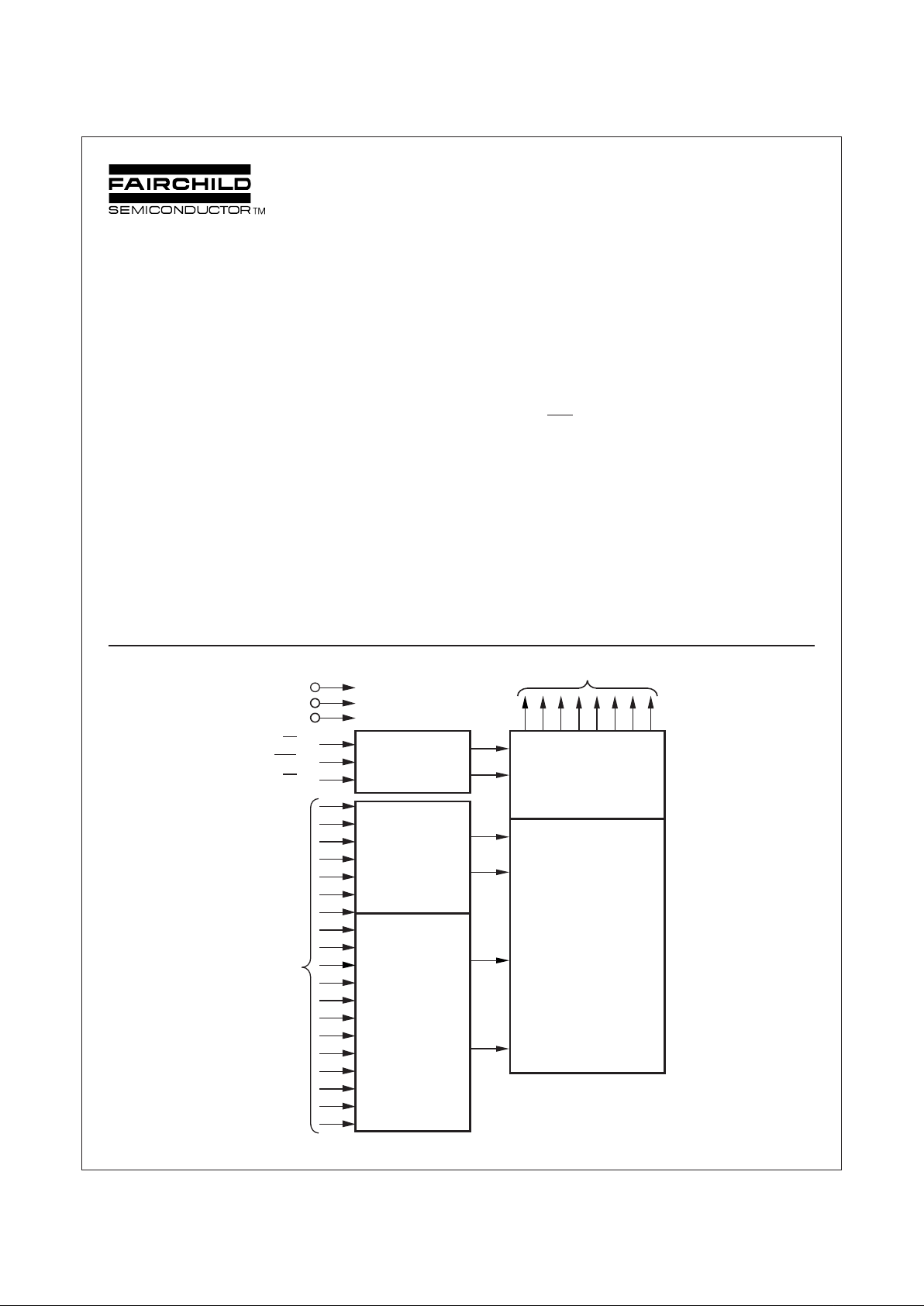
Block Diagram
July 1998
Features
■ High performance CMOS
— 100 ns access time
■ Simplified upgrade path
—VPP and PGM are “Don’t Care” during normal read
operation
■ Manufacturers identification code
■ JEDEC Standard Pin Configuration
— 32-pin CERDIP package
— 32-pin PLCC package
— 32-pin PDIP package
© 1998 Fairchild Semiconductor Corporation
Output Enable,
Chip Enable, and
Program Logic
Y Decoder
X Decoder
. . . . . . . . .
Output
Buffers
2,097,152-Bit
Cell Matrix
Data Outputs O0 - O
7
V
CC
GND
V
PP
OE
PGM
CE
A0 - A
17
Address
Inputs
DS010835-1
2
www.fairchildsemi.com
NM27C020 2,097,152-Bit (256K x 8) UV Erasable CMOS EPROM
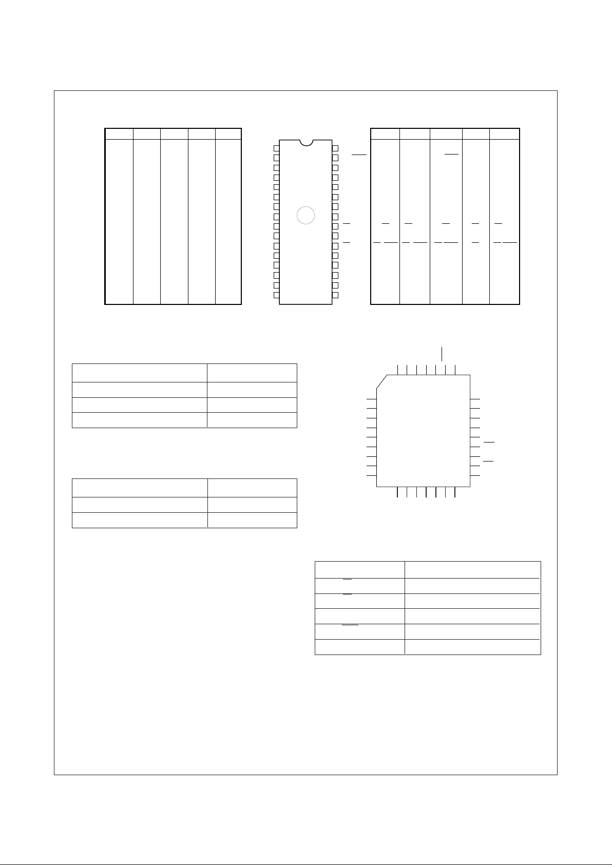
Connection Diagrams
Commercial Temperature Range
(0°C to +70°C) VCC = 5V ±10%
Parameter/Order Number Access Time (ns)
NM27C020 Q, V, N 100 100
NM27C020 Q, V, N 120 120
NM27C020 Q, V, N 150 150
All versions are guaranteed to function at slower speeds.
Extended Temperature Range
(-40°C to +85°C) VCC = 5V ±10%
Parameter/Order Number Access Time (ns)
NM27C020 QE, VE, TE, NE 120 120
NM27C020 QE, VE, TE, NE 150 150
PLCC Pin Configuration
Top View
Pin Names
A0 –A17 Addresses
CE Chip Enable
OE Output Enable
O0 –O7 Outputs
PGM Program
XX Don’t Care (During Read)
1
2
3
4
5
6
7
8
9
10
11
12
13
14
15
16
32
31
30
29
28
27
26
25
24
23
22
21
20
19
18
17
XX/V
PP
A
16
A
15
A
12
A
7
A
6
A
5
A
4
A
3
A
2
A
1
A
0
O
0
O
1
O
2
GND
A
15
A
12
A
7
A
6
A
5
A
4
A
3
A
2
A
1
A
0
O
0
O
1
O
2
GND
27C512 27C256
V
PP
A
12
A
7
A
6
A
5
A
4
A
3
A
2
A
1
A
0
O
0
O
1
O
2
GND
27C256 27C512
V
CC
XX/PGM
A
17
A
14
A
13
A
8
A
9
A
11
OE
A
10
CE
O
7
O
6
O
5
O
4
O
3
V
CC
A
14
A
13
A
8
A
9
A
11
OE
A
10
CE/PGM
O
7
O
6
O
5
O
4
O
3
V
CC
A
14
A
13
A
8
A
9
A
11
OE/V
PP
A
10
CE/PGM
O
7
O
6
O
5
O
4
O
3
XX/V
PP
A
16
A
15
A
12
A
7
A
6
A
5
A
4
A
3
A
2
A
1
A
0
O
0
O
1
O
2
GND
27C040
XX/V
PP
A
16
A
15
A
12
A
7
A
6
A
5
A
4
A
3
A
2
A
1
A
0
O
0
O
1
O
2
GND
27C010
A19
A
16
A
15
A
12
A
7
A
6
A
5
A
4
A
3
A
2
A
1
A
0
O
0
O
1
O
2
GND
27C080 27C040 27C080
V
CC
A
18
A
17
A
14
A
13
A
8
A
9
A
11
OE
A
10
CE
O
7
O
6
O
5
O
4
O
3
V
CC
A
18
A
17
A
14
A
13
A
8
A
9
A
11
OE/V
PP
A
10
CE/PGM
O
7
O
6
O
5
O
4
O
3
27C010
V
CC
XX/PGM
XX
A
14
A
13
A
8
A
9
A
11
OE
A
10
CE/PGM
O
7
O
6
O
5
O
4
O
3
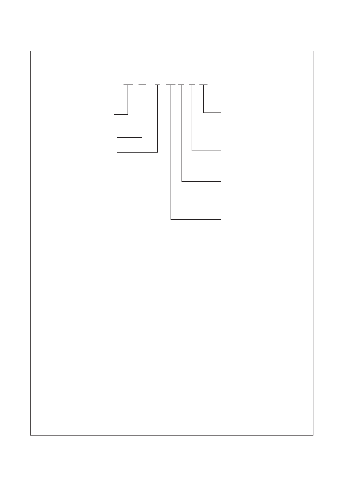
Note: Compatible EPROM pin configurations are shown in the blocks adjacent to the NM27C020 pins.
A14
A13
A8
A9
A11
OE
A10
CE
O7
A7
A6
A5
A4
A3
A2
A1
A0
O0
A12
A15
A16
VPP
VCC
PGM
A17
O1
O2
GND
O3O4O5
O6
5
6
7
8
9
10
11
12
13
29
28
27
26
25
24
23
22
21
14 15 16 17 18 19 20
4 3 2 1 32 31 30
DS010835-10
DS010835-3
3
www.fairchildsemi.com
NM27C020 2,097,152-Bit (256K x 8) UV Erasable CMOS EPROM
Access Time
100 = 100 ns
120 = 120 ns
150 = 150 ns
Operating Temp
Blank = Commercial Temp.
E = Extended Temp.
Packaging
Q = Ceramic DIP
V = PLCC
N = PDIP
Memory Size
020 = 2 Mbit
Fairchild
Memory
EPROM
CMOS
Q 150ENM 27 C 020
Connection Diagrams (Continued)
Ordering Information
DS010835-9
4
www.fairchildsemi.com
NM27C020 2,097,152-Bit (256K x 8) UV Erasable CMOS EPROM
Absolute Maximum Ratings (Note 1)
Storage Temperature -65°C to +125°C
All Input Voltage Except A9 with
Respect to Ground (Note 13) -0.6V to +7V
VPPand A9 with Respect to Ground -0.6V to +14V
VCC Supply Voltage with
Respect to Ground -0.6V to +7V
ESD Protection >2000V
All Output Voltages with
Respect to Ground (Note 13) VCC + 10V to GND -0.6V
Operating Range
Range Temperature VCCTolerance
Commercial 0°C to +70°C +5V ±10
Industrial -40°C to +85°C +5V ±10%
DC Read Characteristics Over Operating Range with V
PP
= V
CC
Symbol Parameter Test Conditions Min Max Units
V
IL
Input Low Level -0.5 0.8 V
V
IH
Input High Level 2.0 VCC +1 V
V
OL
Output Low Voltage IOL = 2.1 mA -0.4 V
V
OH
Output High Voltage IOH = -400 µA 3.5 V
I
SB1
(Note 4) VCC Standby Current (CMOS) CE = VCC ± 0.3V 100 µA
I
SB2
VCC Standby Current (TTL) CE = V
IH
1mA
I
CC
(Note 2) VCC Active Current CE, OE = V
IL
Commercial 30
I/O = 0 mA, f = 5 MHz Industrial 30 mA
Inputs = VIH or V
IL
I
PP
VPP Supply Current VPP = V
CC
10 µA
VPP VPP Read Voltage VCC - 0.4 V
CC
V
I
LI
Input Load Current VIN = 5.5 or GND -1 1 µA
I
LO
Output Leakage Current V
OUT
= 5.5V or GND -10 10 µA
AC Read Characteristics Over Operating Range with V
PP
= V
CC
Symbol Parameter 100 120 150 Units
Min Max Min Max Min Max
t
ACC
Address to Output Delay 100 120 150 ns
t
CE
CE to Output Delay 100 120 150 ns
t
OE
OE to Output Delay 40 45 50 ns
tDF (Note 3) Output Disable to Output Float 40 45 50 ns
t
OH
Output Hold from Addresses, CE 0 0 0 ns
or OE , Whichever Occurred First
Note 1: Stresses above those listed under "Absolute Maximum Ratings" may cause permanent damage to the device. This is a stress rating only and functional operation of
the device at these or any other conditions above those indicated in the operational sections of this specification is not implied. Exposure to absolute maximum rating conditions
for extended periods of time may affect device reliability.
Note 2: The supply current is the sum of ICC and IPP. The maximum current value is with Outputs O0 to O7 unloaded.
Note 3: This parameter is only sampled and is not 100% tested. Output Float is defined as the point where data is no longer driven-see timing diagram.
Note 4: CMOS inputs: VIL = GND 10.3V, VIH = VCC 10.3V.
5
www.fairchildsemi.com
NM27C020 2,097,152-Bit (256K x 8) UV Erasable CMOS EPROM
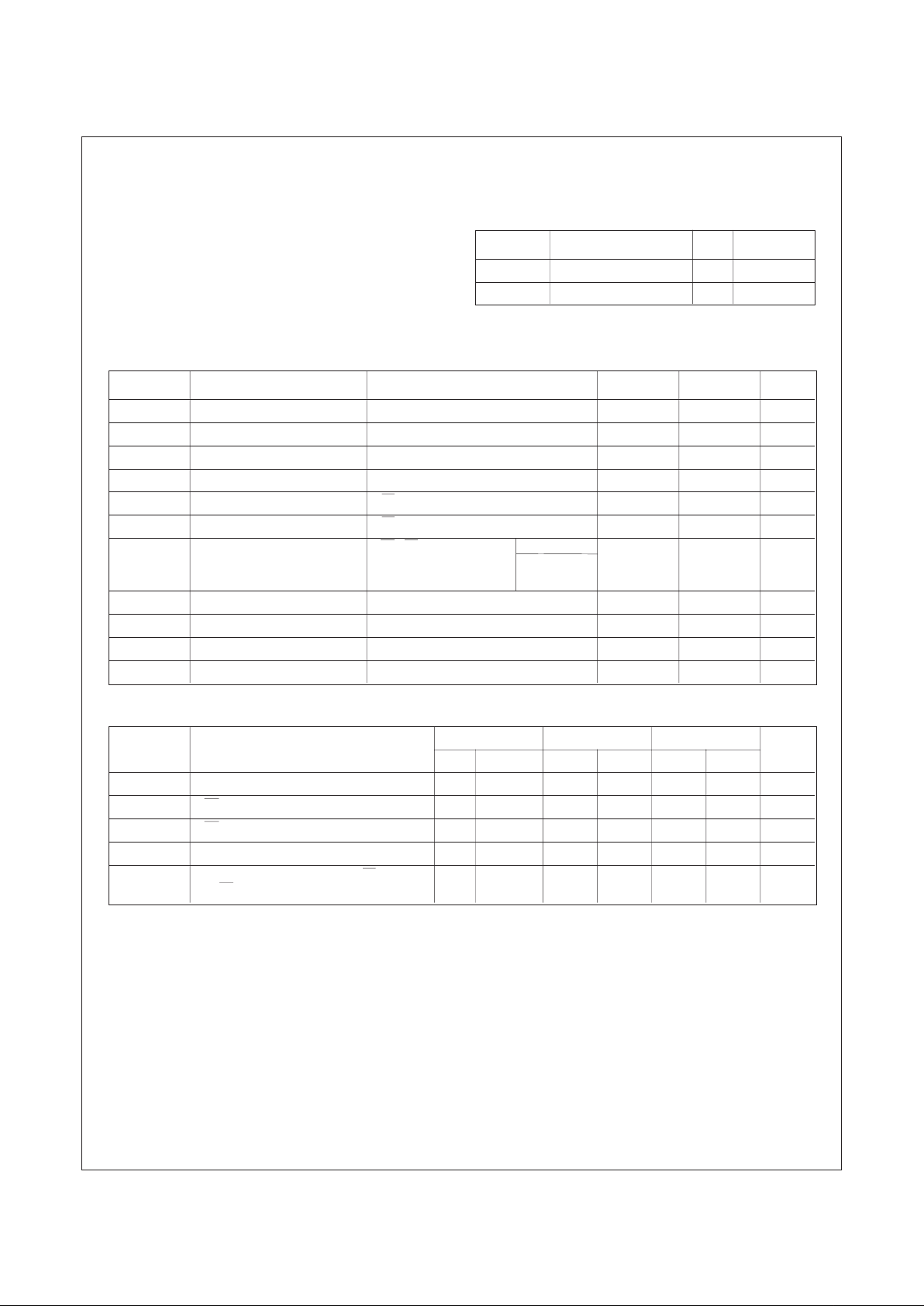
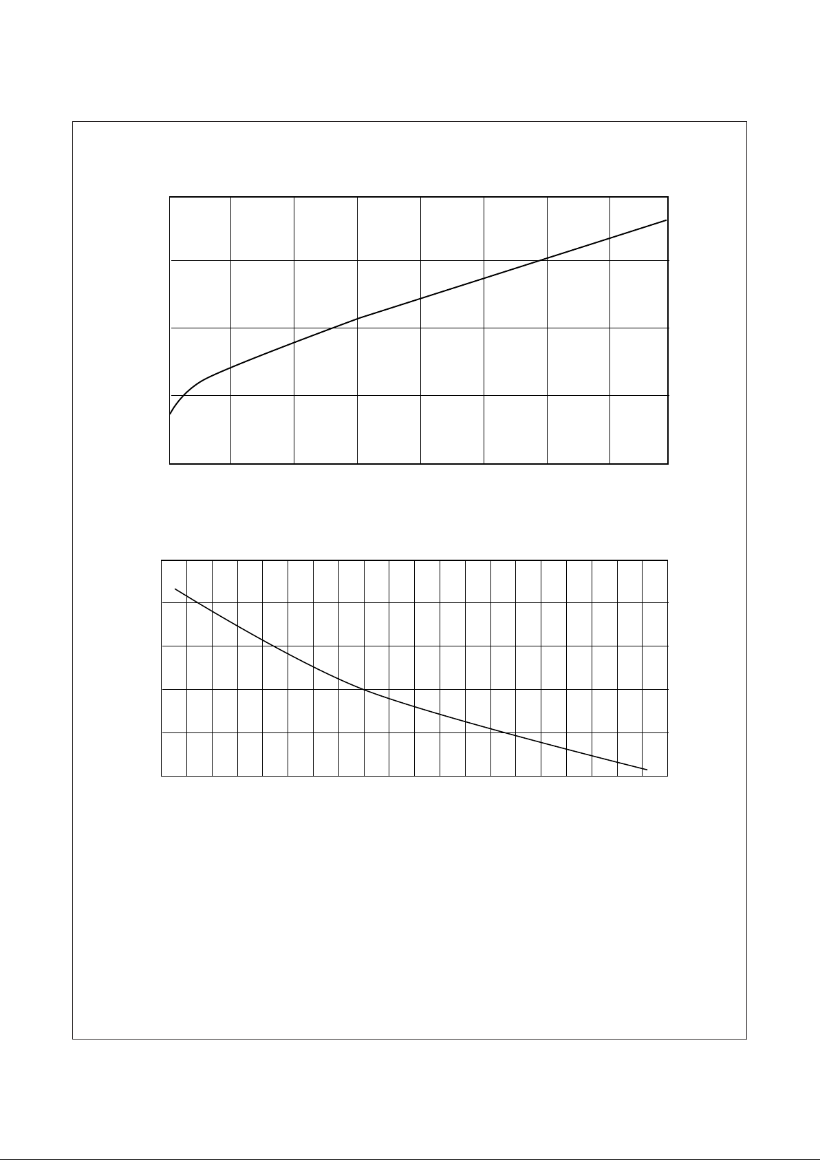
40
30
20
10
0
012345678
31
30
29
28
27
26
-60 -50 -40 -30 -20 -10 0 10 20 30 40 50 60 70 80 90 100 110 120 130 140
AC Read Characteristics (Continued)
ICC vs. Frequency
Frequency (MHz)
ICC vs. Temperature
Temperature (IC)
DS010835-7
DS010835-8
 Loading...