

Fairchild Semiconductor NC7WZ17 Datasheet
NC7WZ17
NC7WZ17 TinyLogic
March 1999
Revised May 2003
TinyLogic
General Description
The NC7WZ17 is a dual buffer with Schmitt trigger inputs
from Fairchild’s Ultra High Speed Series of TinyLogic
the SC70 6-lead package. The device is fabricated with
advanced CMOS technolog y to achieve ultra high speed
with high output drive while maintaining low static power
dissipation over a very broad V
device is specified to o perate over the 1.65V to 5.5V V
range. The input s and outputs are high impedance when
V
is 0V. Inputs tolerate voltages up to 7V independent of
CC
operating voltage. Schmitt trigger inputs typically
V
CC
achieve 1V hysteresis between the positive going and negative going input threshold voltage at 5V V
UHS Dual Buffer with Schmitt Trigger Inputs
Features
■ Space saving SC70 6-l ead package
operating range. The
CC
.
CC
in
■ Ultra small MicroPak
■ Ultra High Speed: t
■ High Output Drive: ±24 mA at 3V V
■ Broad VCC Operating Range; 1.65V to 5.5V
CC
■ Matches the performance of LCX when operated at
3.3V V
CC
■ Power down high impedance inputs/outputs
■ Overvoltage tolerant inputs facilitate 5V to 3V translation
■ Patented noise/EMI reduction circuitry implemented
leadless package
3.6 ns Typ into 50 pF at 5V V
PD
CC
CC
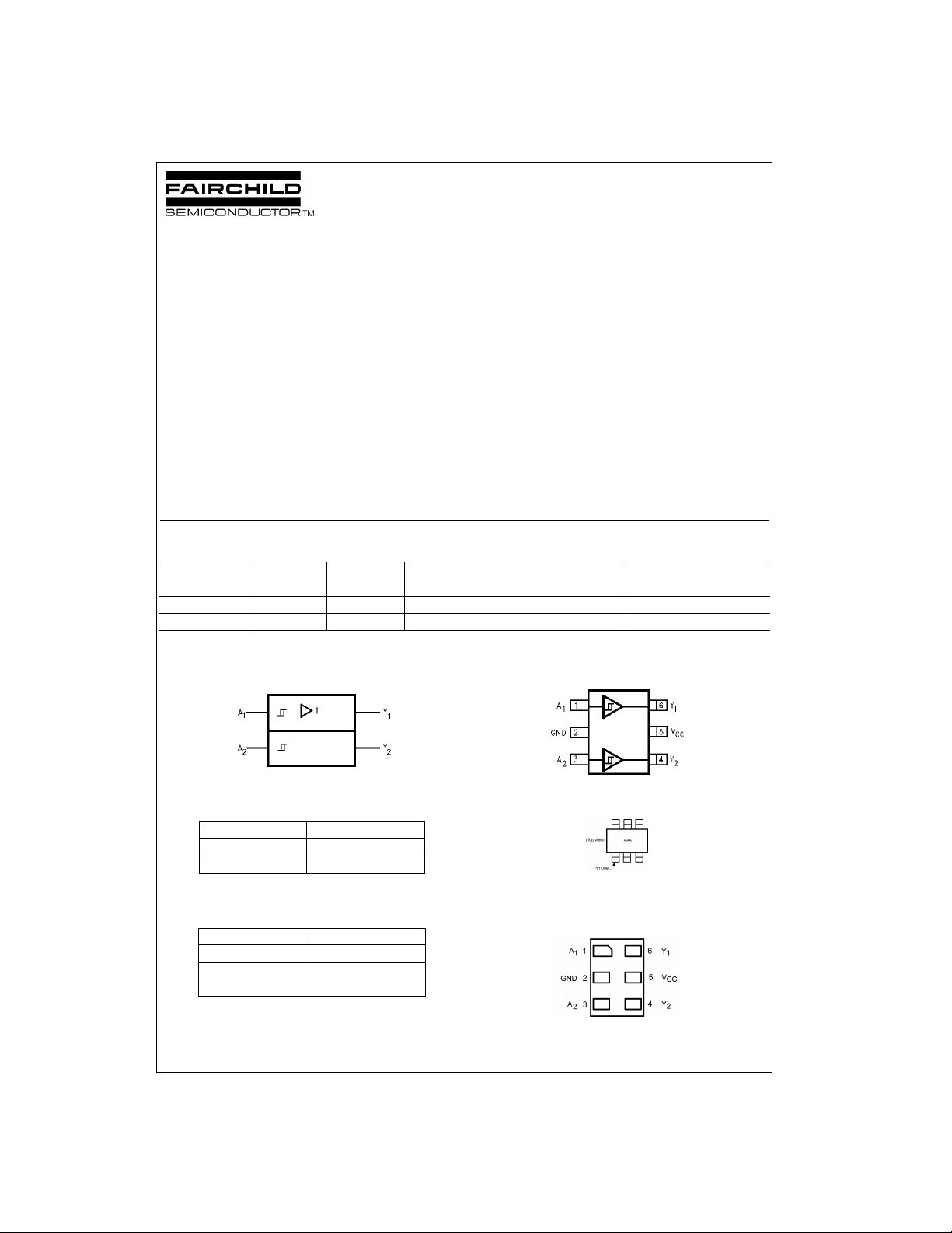
Ordering Code:
Order Package Product Code
Number Number Top Mark
NC7WZ17P6X MAA06A Z17 6-Lead SC70, EIAJ SC88, 1.25mm Wide 3k Units on Tape and Reel
NC7WZ17L6X MAC06A A5 6-Lead MicroPak, 1.0mm Wide 5k Units on Tape and Reel
Logic Symbol
IEEE/IEC
Package Description Supplied As
Connection Diagrams
Pin Assignments for SC 70
UHS Dual Buffer with Schmitt T rigger Inputs
(Top View)
Pin Descriptions
Pin Names Description
A
, A
1
2
Y
, Y
1
2
Function Table
Input Output
AY
LL
HH
H = HIGH Logic Le v el L = LOW Logic Lev el
TinyLogic is a registered tradema rk of F airc hild Semiconduct or Corporation.
MicroPak is a tradem ark of Fairchild Semiconductor Corporation.
© 2003 Fairchild Semiconductor Corporation DS500217 www.fairchildsemi.com
Y = A
Data Inputs
Output
AAA represents Product Code Top Mark - see ordering code
Note: Orientation of Top Mark determines Pin On e locat ion. R ead the Top
Product Code Mark left to right, Pin One is the lower left pin (see diagram).
Pin One Orientation Diagram
Pad Assignments for MicroPak
(Top Thru View)
Absolute Maximum Ratings(Note 1) Recommended Operating
Supply Voltage (VCC) −0.5V to +7V
DC Input Voltage (V
NC7WZ17
DC Output Voltage (V
DC Input Diode Current (I
@ V
< −0.5V −50 mA
IN
DC Output Diode Current (I
< −0.5V −50 mA
@ V
OUT
DC Output Current (I
DC V
/GND Current (ICC/I
CC
Storage Temperature (T
Junction Temperature under Bias (T
Junction Lead Temperature (T
) −0.5V to +7V
IN
) −0.5V to +7V
OUT
)
IK
)
OK
) ±50 mA
OUT
) ±100 mA
GND
) −65°C to +150°C
STG
) 150°C
J
)
L
(Soldering, 10 seconds) 260
Power Dissipation (P
) @ +85°C 180 mW
D
Conditions
Supply Voltage Operating (V
Supply Voltage Data Retention (V
Input Voltage (V
Output Voltage (V
Operating Temperature (TA) −40°C to +85°C
Thermal Resistance (
Note 1: Absolute maximum ratings are DC values beyond which the devi ce
may be damage d or h ave its us eful life im pai red. Th e dat as heet sp ecific ations should be met, without exception, to ensure that the system design is
reliable over its power supply, temperature, and output/input loading variables. Fairchild does no t recommend operation outsid e datasheet spec ifi-
°C
cations.
Note 2: Unused inputs must be held HIGH or LOW. They may not float.
(Note 2)
) 1.65V to 5.5V
CC
)0V to 5.5V
IN
) 0V to V
OUT
θ
)350°C/W
JA
DC Electrical Characteristics
Symbol Parameter
V
P
V
N
V
H
V
OH
Positive Threshold 1.65 0.6 1.0 1.4 0.6 1.11
Voltage 1.8 0.7 1.07 1.5 0.7 1.5
Negative Threshold 1.65 0.2 0.5 0.8 0.2 0.8
Voltage 1.8 0.25 0.56 0.9 0.25 0.9
Hysteresis Voltage 1.65 0.1 0.48 0.9 0.1 0.9
HIGH Level Output 1.65 1.55 1.65 1.55
Voltage 1.8 1.7 1.8 1.7
V
CC
(V) Min Typ Max Min Max
2.3 1.0 1.38 1.8 1.0 1.8
3.0 1.3 1.74 2.2 1.3 2.2
4.5 1.9 2.43 3.1 1.9 3.1
5.5 2.2 2.88 3.6 2.2 3.6
2.3 0.40 0.75 1.15 0.40 1.15
3.0 0.6 0.98 1.5 0.6 1.5
4.5 1.0 1.42 2.0 1.0 2.0
5.5 1.2 1.68 2.3 1.2 2.3
1.8 0.15 0.51 1.0 0.15 1.0
2.3 0.25 0.62 1.1 0.25 1.1
3.0 0.4 0.76 1.2 0.4 1.2
4.5 0.6 1.01 1.5 0.6 1.5
5.5 0.7 1.20 1.7 0.7 1.7
2.3 2.2 2.3 2.2
3.0 2.9 3.0 2.9
4.5 4.4 4.5 4.4
1.65 1.29 1.52 1.29 IOH = −4 mA
2.3 1.9 2.14 1.9 IOH = −8 mA
3.0 2.4 2.75 2.4 IOH = −16 mA
3.0 2.3 2.62 2.3 IOH = −24 mA
4.5 3.8 4.13 3.8 IOH = −32 mA
TA = +25°CT
= −40°C to +85°C
A
) 1.5V to 5.5V
CC
Units Conditions
V
V
V
IOH = −100 µA
VVIN = V
IH
CC
www.fairchildsemi.com 2
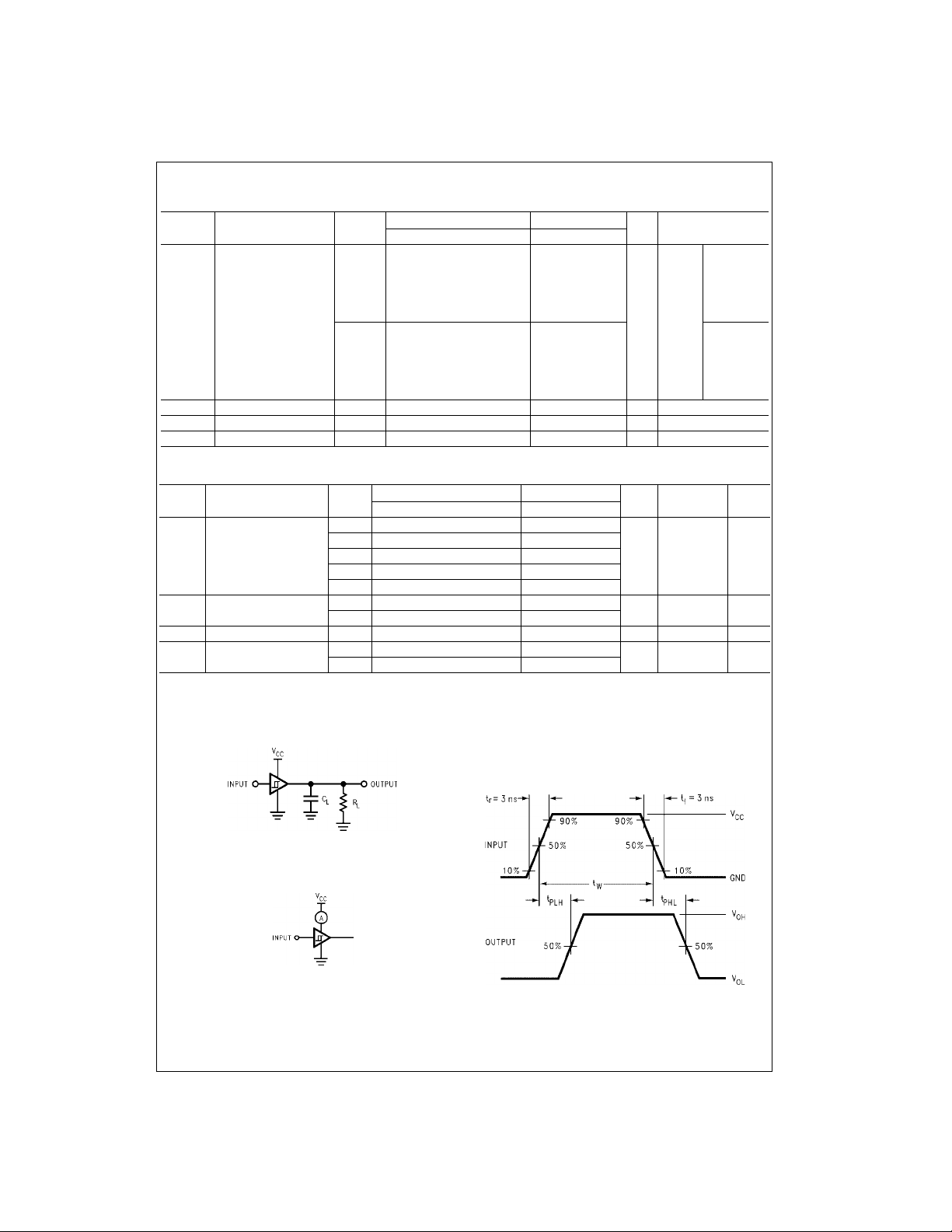
DC Electrical Characteristics (Continued)
NC7WZ17
Symbol Parameter
V
OL
LOW Level Output 1.65 0.0 0.1 0.1
V
CC
(V) Min Typ Max Min Max
TA = +25°CT
= −40°C to +85°C
A
Units Conditions
Voltage 1.8 0.0 0.1 0.1
2.3 0.0 0.1 0.1
3.0 0.0 0.1 0.1
4.5 0.0 0.1 0.1
1.65 0.08 0.24 0.24 IOL = 4 mA
VVIN = V
2.3 0.10 0.3 0.3 IOL = 8 mA
3.0 0.16 0.4 0.4 I
3.0 0.24 0.55 0.55 I
4.5 0.25 0.55 0.55 IOL = 32 mA
I
IN
I
OFF
I
CC
Input Leakage Current 0 to 5.5 ±0.1 ±1.0 µAVIN = 5.5V, GND
Power Off Leakage Current 0.0 1 10 µAVIN or V
Quiescent Supply Current 1.65 to 5.5 1.0 10 µAVIN = 5.5V, GND
AC Electrical Characteristics
V
Symbol Parameter
t
t
Propagation Delay 1.65 2.0 8.3 14.3 2.0 15.8
PLH
PHL
CC
(V) Min Typ Max Min Max Number
1.8 2.0 6.9 11.9 2.0 13.1 CL = 15 pF,
2.5 ± 0.2 1.5 4.8 8.2 1.5 9.0 R
3.3 ± 0.3 1.0 3.7 5.6 1.0 6.2
5.0 ± 0.5 0.8 3.0 4.7 0.8 5.2
t
t
C
C
Propagation Delay 3.3 ± 0.3 1.5 4.3 6.6 1.5 7.3
PLH
PHL
Input Capacitance 0 2.5 pF
IN
Power Dissipation 3.3 10
PD
5.0 ± 0.5 1.0 3.6 5.6 1.0 6.2 RL = 500Ω
Capacitance 5.0 12
Note 3: CPD is defined as the value of the internal equivalent capacitance which is derived from dynamic operating current consumption (I
loading and operating at 50% duty cycle. (See Figure 2.) C
= (CPD)(VCC)(fIN) + (ICCstatic).
I
CCD
TA = +25°CT
is related to I
PD
dynamic operating current by the express ion:
CCD
= −40°C to +85°C
A
Units Conditions
ns
L
CL = 50 pF,
ns
pF (Note 3) Figure 2
IL
= 1 MΩ
CCD
IOL = 100 µA
= 16 mA
OL
= 24 mA
OL
= 5.5V
OUT
) at no output
Figure
Figures
1, 3
Figures
1, 3
AC Loading and Waveforms
CL includes load and s tr ay c apacitance
Input PR R = 1.0 MHz; t
Input = AC Wavefor m; tr = tf = 1.8 ns;
PRR = variable; Duty Cycle = 50%
= 500 ns
W
FIGURE 1. AC Test Circuit
FIGURE 2. I
Test Circuit
CCD
FIGURE 3. AC Waveforms
3 www.fairchildsemi.com
 Loading...