

Fairchild Semiconductor NC7WZ02 Datasheet
NC7WZ02
NC7WZ02 TinyLogic
April 2000
Revised April 2003
TinyLogic
General Description
The NC7WZ02 is a dual 2-Input NOR Gate from Fairchild’s
Ultra High Speed Series of TinyLogic
cated with advanced CMOS technology to achieve ultra
high speed with high output drive while maintaining low
static power dissipati on over a very broad V
range. The device is s pecified to operate over the 1.6 5V to
range. The inputs and output are high impedance
5.5V V
CC
when V
dent of V
is 0V. Inputs tolerate voltages up to 7V indepen-
CC
CC
UHS Dual 2-Input NOR Gate
Features
■ Space saving US8 surface mount package
■ MicroPak
■ Ultra High Speed: t
■ High Output Drive: ±24 mA at 3V V
■ Broad VCC Operating Range: 1.65V to 5.5V
■ Matches the performance of LCX when operated at
■ Power down high impedance inputs/output
■ Overvoltage tolerant inputs facilitate 5V to 3V
■ Patented noise/EMI reduction circuitry implemented
operating voltage.
. The device is fabr i -
operating
CC
3.3V V
CC
translation
leadless package
2.4 ns typ into 50 pF at 5V V
PD
CC
CC
Ordering Code:
Product
Package Description Supplied AsOrder Package Code
Number Number Top Mark
NC7WZ02K8X MAB08A WZ02 8-Lead US8, JEDEC MO-187, Variation CA 3.1mm Wide 3k Units on Tape and Reel
NC7WZ02L8X
(Preliminary)
MAC08A P5 8-Lead MicroPak, 1.6 mm Wide 5k Units on Tape and Reel
UHS Dual 2-Input NOR Gate
TinyLogic is a registered trademark of F airc hild Semiconduct or Corporation.
MicroPak is a tradem ark of Fairchild Semiconductor Corporation.
© 2003 Fairchild Semiconductor Corporation DS500269 www.fairchildsemi.com
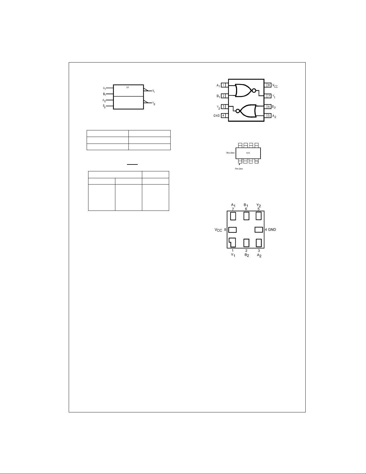
Logic Symbol
NC7WZ02
Pin Descriptions
Pin Names Description
A
Function Table
ABY
LLH
LHL
HLL
H = HIGH Logic Level
L = LOW Logic Level
HHL
IEEE/IEC
, B
n
n
Y
n
Y
= A + B
Inputs Output
Inputs
Output
Connection Diagrams
(Top View)
Pin One Orientation Diagram
AAA represents Product Code Top Mark - see ordering cod e
Note: Orientation of Top Mark determines Pin One location. Read the top
product code mark lef t to right, Pin One is the lo w er left pin (see diagram ).
Pad Assignments for MicroPak
www.fairchildsemi.com 2
(Top Thru View)
Absolute Maximum Ratings(Note 1) Recommended Operating
Supply Voltage (VCC) −0.5V to +7V
DC Input Voltage (V
DC Output Voltage (V
DC Input Diode Current (I
@ V
< −0.5V −50 mA
IN
DC Output Diode Current (I
< −0.5V −50 mA
@ V
OUT
DC Output Current (I
DC V
/GND Current (ICC/I
CC
Storage Temperature (T
Junction Temperature under Bias (T
Junction Lead Temperature (T
) −0.5V to +7V
IN
) −0.5V to +7V
OUT
)
IK
)
OK
) ± 50 mA
OUT
) ± 100 mA
GND
) −65°C to +150°C
STG
) 150°C
J
);
L
(Soldering, 10 seconds) 260
Power Dissipation (P
) @ +85°C 250 mW
D
Conditions
Supply Voltage Operating (V
Supply Voltage Data Retention (V
Input Voltage (V
Output Voltage (V
Operating Temperature (TA) −40°C to +85°C
Input Rise and Fall Time (t
@ 1.8V ± 0.15V, 2.5V ± 0.2V 0 ns/V to 20 ns/V
V
CC
V
@ 3.3V ± 0.3V 0 ns/V to 10 ns/V
CC
V
@ 5.0V ± 0.5V 0 ns to 5 ns/V
CC
Thermal Resistance (
°C
Note 1: Absolute maximum ratings are DC values beyond which t he devi ce
may be damag ed or hav e it s usefu l li fe i mpa ired. Th e da tas heet sp ecific ations should be met, without exception, to ensure that the system design is
reliable over its power supply, temperature, and output/input loading variables. Fairchild does not recommend operation outside datasheet specifications.
Note 2: Unused inputs must be held HIGH or LOW. They may not float.
(Note 2)
) 1.65V to 5.5V
CC
) 1.5V to 5.5V
) 0V to 5.5V
IN
)0V to V
OUT
θ
JA
CC
, tf)
r
)250°C/W
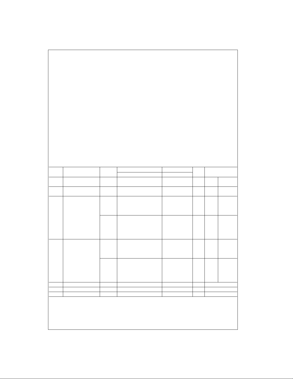
DC Electrical Characteristics
Symbol Parameter
V
HIGH Level Input Voltage 1.65 to 1.95 0.75 V
IH
V
LOW Level Input Voltage 1.65 to 1.95 0.25 V
IL
V
HIGH Level Output Voltage 1.65 1.55 1.65 1.55
OH
V
LOW Level Output Voltage 1.65 0.0 0.1 0.1
OL
I
Input Leakage Current 0 to 5.5 ±0.1 ±1.0 µAVIN = 5.5V, GND
IN
I
Power Off Leakage Current 0.0 1 10 µAVIN or V
OFF
I
Quiescent Supply Current 1.65 to 5.5 1 10 µAVIN = 5.5V, GND
CC
V
CC
(V) Min Typ Max Min Max
2.3 to 5.5 0.7 V
2.3 to 5.5 0.3 V
2.3 2.2 2.3 2.2
3.0 2.9 3.0 2.9
4.5 4.4 4.5 4.4
1.65 1.29 1.52 1.29
2.3 1.9 2.15 1.9 I
3.0 2.4 2.80 2.4 I
3.0 2.3 2.68 2.3 I
4.5 3.8 4.20 3.8 I
2.3 0.0 0.1 0.1
3.0 0.0 0.1 0.1
4.5 0.0 0.1 0.1
1.65 0.08 0.24 0.24
2.3 0.10 0.3 0.3 I
3.0 0.15 0.4 0.4 I
3.0 0.22 0.55 0.55 I
4.5 0.22 0.55 0.55 I
TA = +25°CT
CC
CC
A
0.75 V
0.7 V
CC
CC
= −40°C to +85°C
CC
CC
0.25 V
0.3 V
CC
Units Conditions
V
CC
V
VVIN = VILI
V
VVIN= VIHI
V
OH
I
= −4 mA
OH
OH
OH
OH
OH
= 100µA
OL
IOL = 4 mA
= 8 mA
OL
= 16 mA
OL
= 24 mA
OL
= 32 mA
OL
= 5.5V
OUT
NC7WZ02
CC
= −100µA
=−8 mA
= −16 mA
= −24 mA
= −32 mA
3 www.fairchildsemi.com
 Loading...