

Fairchild Semiconductor NC7WBD3306 Datasheet
NC7WBD3306
NC7WBD3306 TinyLogic
May 2000
Revised April 2003
TinyLogic
UHS 2-Bit Low Power Bus Switch
with Level Shifting
General Description
The NC7WBD3306 is a 2-bit ultra h igh-speed CMOS FET
bus switch with enhanced level shifti ng circuitry and with
TTL-compatible active LOW control inputs. The low On
Resistance of the switch allows inputs to be connected to
outputs with minimal p ropag ation del ay and witho ut gene rating additional groun d bounce noise. The d evice is organized as a 2-bit sw itch with indepe ndent bus enab le (OE
controls. When OE
connected to Port B. When OE
OPEN and a high-impedance sta te exist s between the two
ports. Reduced voltag e drive to the gat e of the FET switch
permits nominal level shifting of 5V to 3V through the
switch. Control inputs tolerate voltages up to 5.5V independent of V
CC
is LOW, the switch is ON and Port A is
is HIGH, the switch is
.
Ordering Code:
Product
Number Number Top Mark
NC7WBD3306K8X MAB08A WB6D 8-Lead US8, JEDEC MO-187, Variation CA 3.1mm Wide 3k Units on T ape and Reel
NC7WBD3306L8X
(Preliminary)
MAC08A P7 8-Lead MicroPak, 1.6 mm Wide 5k Units on Tape and Reel
Features
■ Space saving US8 surface mount package
■ MicroPak
■ Typical 3
■ Level shift facilitates 5V to 3.3V interfacing
■ Minimal propagation delay through the switch
)
■ Power down high impedance input/output
■ Zero bounce in flow through mode
■ TTL compatible active LOW control inputs
■ Control inputs are overvoltage tolerant
Package Description Supplied AsOrder Package Code
leadless package
Ω switch resistance at 5.0V V
, VIN = 0V
CC
UHS 2-Bit Low Power Bus Switch with Level Shifting
TinyLogic is a registered tradema rk of F airc hild Semiconductor Corporation.
MicroPak is a tradem ark of Fairchild Semiconductor Corporation.
© 2003 Fairchild Semiconductor Corporation DS500375 www.fairchildsemi.com
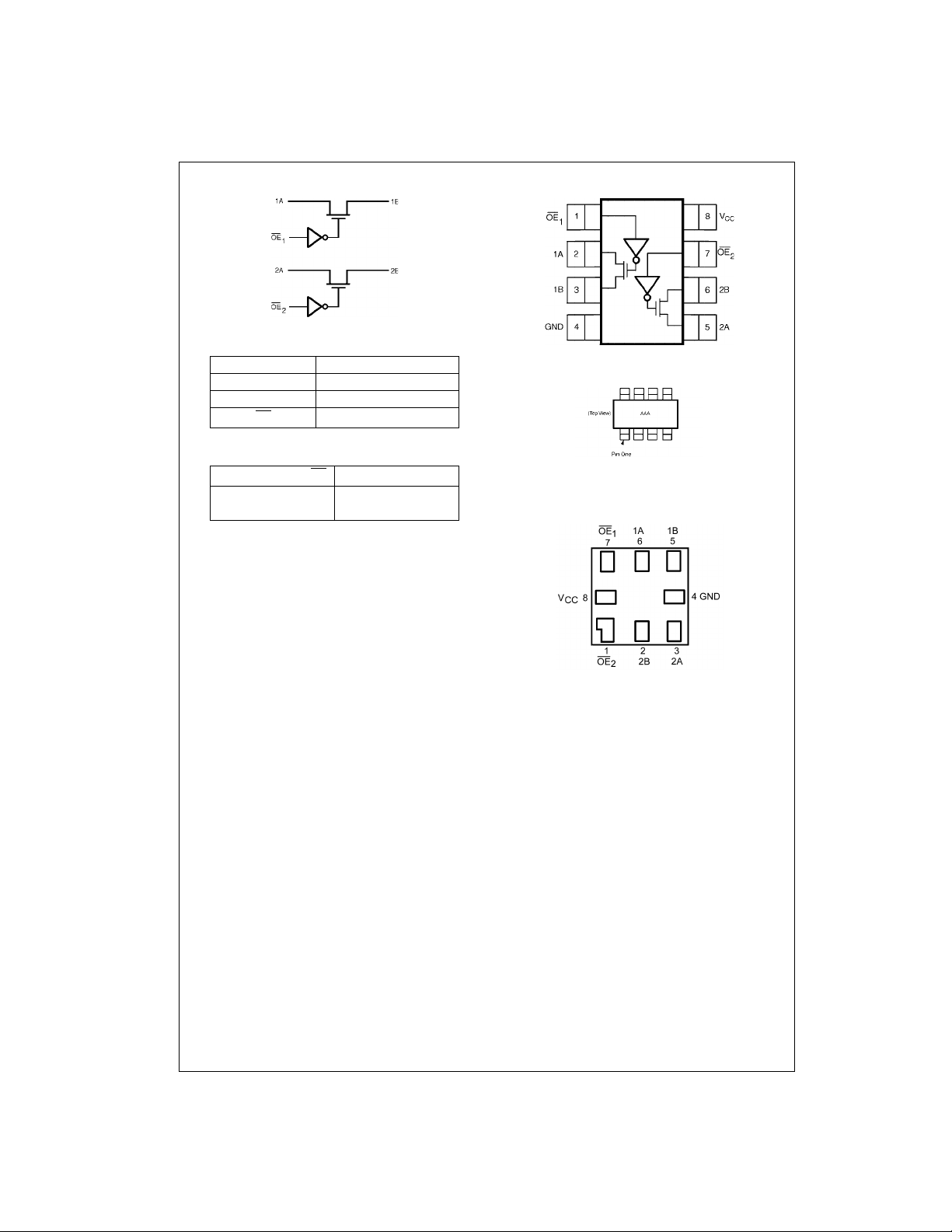
Logic Diagram
NC7WBD3306
Connection Diagrams
Pin Descriptions
Pin Name Description
A Bus A Switch I/O
B Bus B Switch I/O
OE
Bus Enable Input
Function Table
Bus Enable Input (OE
L B Connected to A
H Disconnected
H = HIGH Logic Level L = LOW Logic Level
)Function
(Top View)
Pin One Orientation Diagram
AAA represents Product Code Top Mark - see ordering cod e
Note: Orientation of Top Mark determines Pin One location. Read the top
product code mark lef t to right, Pin One is the lo w er left pin (see diagram ).
Pad Assignments for MicroPak
(Top Thru View)
www.fairchildsemi.com 2
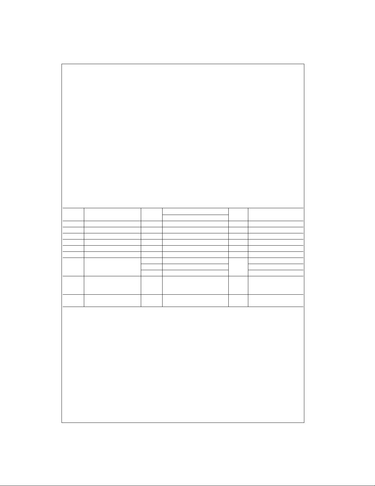
Absolute Maximum Ratings(Note 1) Recommended Operating
Supply Voltage (VCC) −0.5V to +7.0V
DC Switch Voltage (V
DC Output Voltage (V
) −0.5V to +7.0V
S
) (Note 2) −0.5V to +7.0V
IN
DC Input Diode Current
) VIN < 0V −50 mA
(I
IK
DC Output (I
DC V
CC
(I
CC/IGND
Storage Temperature Range (T
) Sink Current 128 mA
OUT
or Ground Current
) ±100 mA
) −65°C to +150°C
STG
Junction Temperature
under Bias (T
Junction Lead Temperature (T
(Soldering, 10 Seconds)
Power Dissipation (P
) +150°C
J
)
L
+260°C
) @ +85°C250 mW
D
Conditions
Supply Operating (V
Control Input Voltage (V
Switch Input Voltage (V
Switch Output Voltage (V
Operating Temperature (T
Input Rise and Fall Time (t
Control Input 0 ns/V to 5 ns
Switch I/O 0 ns/V to DC
Thermal Resistance (
Note 1: The “Absolute Maxi mum Ratings ” are those val ues beyond w hich
the safety of the d evice cannot b e guaranteed . The device sh ould not be
operated at these limit s. The parametric values defi ned in the Electrical
Characteristics tab les are not guaranteed a t t he absolute maximum rat ings.
The “Recommend ed O peratin g Cond itions” t able w ill defin e the condition s
for actual device operation.
Note 2: The input and output negative voltage ratings may be exceeded if
the input and ou t put diode current ratings ar e observed.
Note 3: Unused logic inputs must be held HIGH or LOW. They may not
float.
(Note 3)
) 4.5V to 5.5V
CC
) 0V to 5.5V
IN
) 0V to 5.5V
IN
) 0V to 5.5V
OUT
) −40°C to +85°C
A
, tf)
r
θ
)250°C/W
JA
DC Electrical Characteristics
V
Symbol Parameter
V
IK
V
IH
V
IL
V
OH
I
IN
I
OFF
R
ON
I
CC
∆ I
Note 4: Measured by the voltage drop between A and B pins at the indicated c urrent through the switch. On Resistanc e is determined by the lower of the
voltages on the two (A or B) pins.
Note 5: Per TTL driven input (V
Clamp Diode Voltage 4.5 −1.2 V IIN = −18 mA
HIGH Level Input Voltage 4.5 to 5.5 2.0 V
LOW Level Input Voltage 4.5 to 5.5 0.8 V
HIGH Level Output Voltage 4.5 to 5.5 see Figure 3 V VIN = V
Input Leakage Current 5.5 ±1.0 µA0 ≤ VIN ≤ 5.5V
Power OFF Leakage Current 5.5 ±1.0 µA0 ≤ A, B ≤ V
Switch On Resistance 4.5 3 7
(Note 4) 4.5 3 7 V
Quiescent Supply Current 5.5 VIN = VCC or GND, I
Increase in ICC per Input
CC
(Note 5) Input Only, Other OE = V
= 3.4V, control input only). A and B pins do not contribute to ICC.
IN
CC
(V) Min Typ Max
4.5 15 50 VIN = 2.4V, IIN = 15 mA
5.5 1 2.5 mA
TA = −40°C to +85°C
1.1 1.5 mA OE
10 µAOE1 = OE2 = V
Units Conditions
CC
VIN = 0V, IIN = 64 mA
Ω
VIN = 3.4V, IO = 0, one Control
CC
= 0V, IIN = 30 mA
IN
= OE2 = GND
1
CC
OUT
NC7WBD3306
= 0
CC
3 www.fairchildsemi.com
 Loading...