

Fairchild Semiconductor NC7WB3125 Datasheet
NC7WB3125
NC7WB3125 TinyLogic
May 2000
Revised April 2003
TinyLogic
General Description
The NC7WB3125 is a 2-bit ultra high-spee d CMOS FET
bus switch with TTL-compatible active LOW control inputs.
The low On Resistance of the switch allows inputs to be
connected to outputs wi th minimal propagation de lay and
without generating additional ground bounce noise. The
device is organized a s a 2-b it switch with indepe ndent b us
enable (OE
and Port A is connect ed to Port B. Whe n OE
switch is OPEN and a high-impedance state exists
between the two ports. C ontrol inputs t olerate voltages up
to 5.5V independent of V
UHS 2-Bit Low Power Bus Switch
) controls. When OE is LOW, the switch is ON
.
CC
is HIGH, the
Features
■ Space saving US8 surface mount package
■ MicroPak
■ Typical 3
■ Minimal propagation delay through the switch
■ Power down high impedance input/output
■ Zero bounce in flow through mode
■ TTL compatible active LOW control inputs
■ Control inputs are overvoltage tolerant
■ Bus switch replacement for Logic x125 part
leadless package
Ω switch resistance at 5.0V V
CC
Ordering Code:
Product
Package Description Supplied AsOrder Package Code
Number Number Top Mark
NC7WB3125K8X MAB08A WB25 8-Lead US8, JEDEC MO-187, Variation CA 3.1mm Wide 3k Units on Tape and Reel
NC7WB3125L8X
(Preliminary)
MAC08A T4 8-Lead MicroPak, 1.6 mm Wide 5k Units on Tape and Reel
UHS 2-Bit Low Power Bus Switch
TinyLogic is a registered tradema rk of F airc hild Semiconduct or Corporation.
MircoPak is a tradem ark of Fairchild Semiconductor Corporation.
© 2003 Fairchild Semiconductor Corporation DS500376 www.fairchildsemi.com
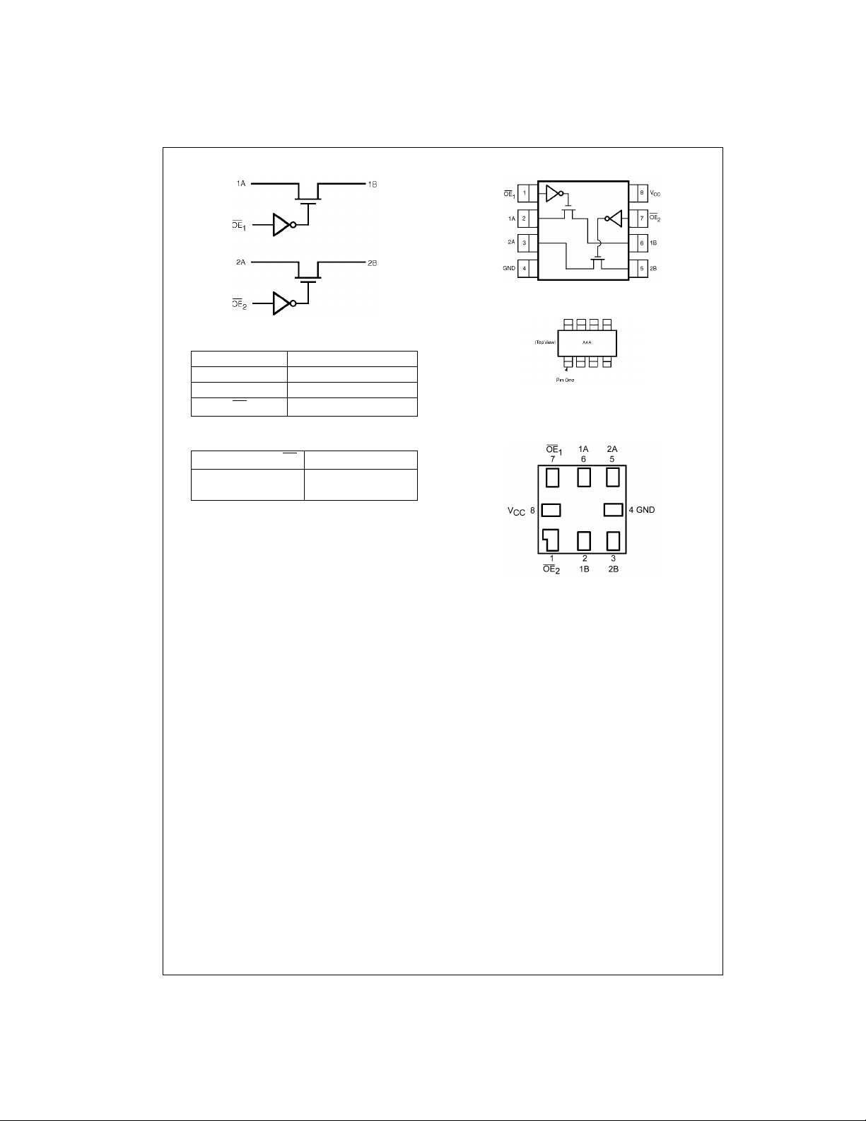
Logic Diagram
NC7WB3125
Pin Descriptions
Pin Name Description
ABus A
BBus B
OE
Function Table
Bus Enable Input
Connection Diagrams
(Top View)
Pin One Orientation Diagram
AAA represents Product Code Top Mark - see ordering cod e
Note: Orientation of Top Mark determines Pin One location. Read the top
product code mark lef t to right, Pin One is the lo w er left pin (see diagram ).
Pad Assignments for MicroPak
Bus Enable Input OE
L B Connected to A
H Disconnected
Function
(Top Thru View)
www.fairchildsemi.com 2
Absolute Maximum Ratings(Note 1) Recommended Operating
Supply Voltage (VCC) −0.5V to +7.0V
DC Switch Voltage (V
DC Output Voltage (V
) −0.5V to +7.0V
S
) (Note 2) −0.5V to +7.0V
IN
DC Input Diode Current
) VIN < 0V −50 mA
(I
IK
DC Output (I
DC V
CC
(I
CC/IGND
Storage Temperature Range (T
Junction Temperature under Bias (T
Junction Lead Temperature (T
(Soldering, 10 Seconds)
Power Dissipation (P
) Current 128 mA
OUT
or Ground Current
) ±100 mA
) −65°C to +150°C
STG
) +150°C
J
)
L
) @ +85°C250 mW
D
+260°C
Conditions
Supply Operating (V
Control Input Voltage (V
Switch Input Voltage (V
Output Voltage (V
Operating Temperature (T
Input Rise and Fall Time (t
Switch Control Input 0 ns/V to 5 ns
Switch I/O 0 ns/V to DC
Thermal Resistance (
Note 1: The “Absolute Maxi mum Ratings ” are those val ues beyond w hich
the safety of the d evice cannot b e guaranteed . The device sh ould not be
operated at these limit s. The parametric values defi ned in the Electrical
Characteristics tables are not gu aranteed at t he absolute m ax imum ratings .
The “Recommend ed O peratin g Cond itions” t able w ill defin e the condition s
for actual device operation.
Note 2: The input and output negative voltage ratings may be exceeded if
the input and ou t put diode current ratings are observed.
Note 3: Unused logic inputs must be held HIGH or LOW. They may not
float.
(Note 3)
) 4.0V to 5.5V
CC
) 0V to 5.5V
IN
) 0V to 5.5V
IN
) 0V to 5.5V
OUT
) −40°C to +85°C
A
, tf)
r
θ
)250°C/W
JA
DC Electrical Characteristics
V
Symbol Parameter
V
IK
V
IH
V
IL
V
OH
I
IN
I
OFF
R
ON
I
CC
∆ I
Note 4: Measured by the voltage drop between A and B pins at the indicated c urrent through the switch. On Resistanc e is determined by the lower of the
voltages on the two (A or B) pins.
Note 5: Per TTL driven input (V
Clamp Diode Voltage 4.5 −1.2 V IIN = −18 mA
HIGH Level Input Voltage 4.0 to 5.5 2.0 V
LOW Level Input Voltage 4.0 to 5.5 0.8 V
HIGH Level Output Voltage 4.0 to 5.5 See Figure 3 V VIN = V
Input Leakage Current 5.5 ±1.0 µA0 ≤ VIN ≤ 5.5V
Switch OFF Leakage Current 5.5 ±1.0 µA0 ≤ A, B ≤ V
Switch On Resistance 4.5 3 7
(Note 4) 4.5 3 7 VIN = 0V, IIN = 30 mA
Quiescent Supply Current 5.5 3 µAVIN = VCC or GND
Increase in ICC per Input (Note 5) 5.5 1 2.5 mA VIN = 3.4V, One OE Input only,
CC
= 3.4V, control input only). A and B pins do not contribute to ICC.
IN
CC
(V) Min Typ Max
4.5 6 15 V
4.0 10 20 V
TA = −40°C to +85°C
Units Conditions
CC
VIN = 0V, IIN = 64 mA
Ω
I
OUT
Other OE = V
CC
= 2.4V, IIN = 15 mA
IN
= 2.4V, IIN = 15 mA
IN
= 0
CC
NC7WB3125
3 www.fairchildsemi.com
 Loading...